how to solve emi problems in isolated automotive systems
TRANSCRIPT
How to Solve EMI Problems in Isolated Automotive SystemsBy Charlie Ice, Senior Product Manager, Isolation, Silicon Labs
2silabs.com/isolation/automotive-isolation
Introduction• Isolated automotive systems face unique
challenges in passing electromagnetic interference testing
• Automotive electromagnetic compatibility is generally governed by the CISPR 25 standard
• Device selection and minor improvements to component placement and PCB design can lead to big improvements in EMI performance
Electromagnetic compatibility (EMC) has long been a
challenge for engineers, and as electric vehicle (EV) and hybrid
electric vehicle (HEV) systems continue to gain momentum,
this continues to be a major concern. Traditional internal
combustion engine (ICE) vehicles are largely mechanical
in nature, with electronics bolted to the mechanical power
plant. EVs and HEVs, however, are very different. Electrical
power is converted into mechanical motion using high-voltage
batteries, motors, and chargers. With great power comes great
responsibility... to limit the electromagnetic interference (EMI)
that comes with power electronics! The isolation used to bridge
the low voltage and high voltage domains also introduces
new EMI concerns. Many modern EVs and HEVs use digital
isolators, which bring unprecedented levels of sophistication
and capability to isolation devices and are designed to minimize
EMI. However, they are still a digital device that can cause EMI
issues. Fortunately, there are several tried and true techniques
for reducing EMI in an isolated system, and three of the most
effective don’t add any additional cost.

3silabs.com/isolation/automotive-isolation
Before tackling EMI improvements, or the EMI standards for vehicles, the basics of electromagnetic compatibility (EMC) and
EMI must be understood. EMC refers to both the immunity and emissions of a device, while EMI focuses only on the emissions
of a device. CISPR 25, the most common EMC standard used for vehicles, specifies both EMI and immunity requirements. A
device’s ability to operate correctly despite the presence of interference is known as immunity. Designers generally place and
emphasis on reducing the EMI of a device because it tends to improve its immunity to outside interference.
EMI is divided into conducted and radiated emission limits within CISPR 25, and the difference between the two is fairly
intuitive. Conducted EMI travels between devices through the power, signaling, or other connected cables. This is in contrast
to radiated EMI, which travels through electromagnetic fields in order to interfere other devices. Radiated EMI, on the other
hand, travels through electromagnetic fields to interfere with the other device. Radios illustrate this concept well because
the radio transmitter is emitting specific frequencies of radiated EMI that the receiver is tuned to pick up. The same holds
true for unwanted radiated EMI - the offending device transmits an unwanted electromagnetic field, which the other device
unintentionally receives and amplifies. Unlike a radio, this received signal results in the device operating unintentionally. EMC
standards for EMI ensure the conducted and radiated emissions are below a specified threshold under specific test conditions.
By passing the EMI tests outlined in CISPR 25, a device is unlikely to interfere with another device in the vehicle.
Differential-mode and common-mode currents are an important part of any discussion about EMI. As common-mode currents
often cause EMI, the vast majority of circuits operate by using differential-mode current. Figure 1 shows a single-ended
signaling scheme using differential-mode current, where current is sent on one conductor and then returned through the ground
connection. Another differential-mode signaling method is to use balanced differential signaling, where a dedicated conductor
is added for the return current, as shown in Figure 2. In both methods, the current in the two conductors is the same leaving a
net zero current. Unfortunately, many times the return current finds an alternative, often longer, path back to the source resulting
in a common-mode current. This common-mode current creates an imbalance in the two conductors which causes radiated
emissions. Figures 3 and 4 show common-mode currents for both single ended and differential-mode systems. Fortunately,
many common-mode currents can be reduced with a few design improvements. Before exploring these methods, however, the
additional challenges brought about by isolation must be discussed.
Immunity, Emissions, and Currents
Figure 1 - Single-ended differential-mode current.
Load(RX)
VS VL
isource
Vdiff
ireturn
Source(TX)

4silabs.com/isolation/automotive-isolation
Figure 2 - Balanced differential-mode current.
Load(RX)
VS VL
isource
Vdiff
ireturn
Source(TX)
Figure 3 - Common-mode current in a single ended system.
Load(RX)
VS VL
isource = idiff + icm
idiff
Source(TX)
icm
Figure 4 - Common-mode current in a differential signaling system.
Load(RX)
VS VL
Source(TX)
isource = idiff + icm
idiff
icm

5silabs.com/isolation/automotive-isolation
Isolation, and digital isolation in particular, is one of the fundamental technologies enabling the electric vehicle revolution. The
isolation device allows communication and signaling across the high impedance barrier between the high voltage and low
voltage domains. Figure 5 shows a basic isolation diagram. Among many other use cases and benefits, the isolation barrier
allows the low voltage electronics, often the controller, to be separated from the high voltage portion of the system. Digital
isolation leverages CMOS technology to replace traditional optocouplers and bring greater sophistication and integration
than ever before to the isolation device. Silicon Labs’ digital isolators use capacitors and high frequency signaling to create
the isolation barrier and pass information across it. To minimize emissions, the internal capacitors are very well matched,
and signals are sent using balanced differential signaling. This requires two capacitors to create a single digital channel, as
shown in Figure 6. Even with these techniques, isolation in a system, and digital isolation technology itself, introduces new EMI
challenges.
EMI Challenges from Isolation
Figure 5 - Isolation creates a very high impedance between two grounds in a system, effectively eliminating the electrical connection between them.
SupplyVoltage A
GroundA
GroundB
Very HighImpedance
Between GroundsA and B
SupplyVoltage B
DC DCCircuit
ACircuit
BSignals
Figure 6 - Silicon Labs digital isolation channel and balanced differential signaling.
Input voltagethreshold
comparatorand OOK
Modulator
+AC
VDDA
Power Domain A Power Domain B
Isol
atio
nBa
rrier
DifferentialRF Carrier
Transmitter
Matched Iso-Capacitors
Silicon Labs Isolator Channel
Ax Input
GNDA
-AC
VDDB
Bx Output
GNDB
Detector andpush-pull
digital output

6silabs.com/isolation/automotive-isolation
The separation of the power domains creates a high impedance path between the two circuits, as shown in Figure 5. This high
impedance path creates a problem for common mode currents induced by large changes in voltage (dv/dt) present on one side
and not the other. These E-field induced currents have to find a path back to their source and their paths are often long, not well
defined, and high impedance. Eventually, the current returns through parasitic capacitance between the power domains. The
large loop area created by these currents can lead to increased conducted and radiated emissions. Minimizing these common
mode currents usually involves placing a capacitor across the isolation barrier (known as a Y capacitor) or even interleaving the
PCB planes to add additional capacitance. This extra capacitance provides a low impedance, short path for the high frequency
current to return to its source. Detailed analysis of Y capacitor placement and PCB inner plane capacitor design can be found
in Silicon Lab’s application note– AN1131: Design Guide for Reducing EMI in Isolated Systems. However, before diving into the
intricacies of E-fields and capacitance calculations, many EMI problems can be solved using traditional EMI best practices with a
few modifications specific to digital isolators. Three of the most common, and successful, come at no additional cost and involve
component selection and careful layout.

7silabs.com/isolation/automotive-isolation
Digital isolators leverage CMOS technology to create the isolation barrier and transmit signals across them. Silicon Labs’ digital
isolators use silicon dioxide to build high voltage capacitors that maintain the isolation barrier. Signals are transmitted across the
capacitive barrier using high frequency RF signals. By leveraging on/off keying (OOK) modulation, the RF transmitter is only active
during one of the two logic states, as shown in Figure 7. The default output configuration determines when an RF transmitter will be
active. If the signal being sent by the isolator is typically either high or low, simply choosing the matching default output state will
minimize the transmissions, reducing EMI and power consumption. For example, when isolating a SPI bus with the idle state high,
selecting an isolator with an output default high decreases the RF transmissions of the isolator. Figure 8 illustrates the difference
between a default low and default high isolator for this SPI bus configuration. In the Silicon Labs’ Si86xx family of digital isolators,
Si86xxBx part numbers use low as their default state, while Si86xxEx default to output high. With the proper digital isolator
selected, the components around the isolation device may now be optimized for EMI.
Method 1: Select the Isolator that Minimizes Transmissions
Figure 7 - Silicon Labs OOK modulation.
Figure 8 - Reducing RF transmissions by selecting the default output state of the isolator.
Ax InputSignal
Bx OutputSignal
On/Off KeyedRF Transmitter
Bus ActivityCS
SCLKSDA
‘E’ Ordering Option Modulated Carrier Transmission
‘B’ Ordering Option Modulated Carrier TransmissionCS
SCLKSDA
CSSCLKSDA
8silabs.com/isolation/automotive-isolation
Virtually every digital isolator specifies using a bypass capacitor on the supply pins, and they have a tremendous impact on the
EMI performance of the system. The bypass capacitors help reduce AC noise on the power rails. Many times, AC noise results
from ripple on the power supply rail due to transient loads from the digital isolator’s normal operation. The bypass capacitors
supply additional current to the device during these transient loads, effectively reducing the ripple on the power supply rail. In
addition, the bypass capacitors short AC noise to ground and prevent it from entering the digital isolator. Careful selection and
placement of the bypass capacitors maximizes their effectiveness.
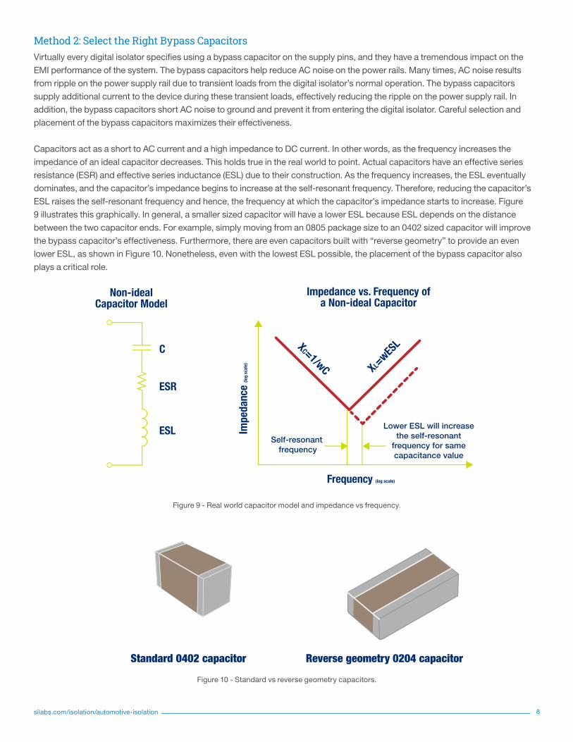
Capacitors act as a short to AC current and a high impedance to DC current. In other words, as the frequency increases the
impedance of an ideal capacitor decreases. This holds true in the real world to point. Actual capacitors have an effective series
resistance (ESR) and effective series inductance (ESL) due to their construction. As the frequency increases, the ESL eventually
dominates, and the capacitor’s impedance begins to increase at the self-resonant frequency. Therefore, reducing the capacitor’s
ESL raises the self-resonant frequency and hence, the frequency at which the capacitor’s impedance starts to increase. Figure
9 illustrates this graphically. In general, a smaller sized capacitor will have a lower ESL because ESL depends on the distance
between the two capacitor ends. For example, simply moving from an 0805 package size to an 0402 sized capacitor will improve
the bypass capacitor’s effectiveness. Furthermore, there are even capacitors built with “reverse geometry” to provide an even
lower ESL, as shown in Figure 10. Nonetheless, even with the lowest ESL possible, the placement of the bypass capacitor also
plays a critical role.
Method 2: Select the Right Bypass Capacitors
Non-idealCapacitor Model
C
Impe
danc
e (lo
g sc
ale)
Frequency (log scale)
Self-resonant frequency
Lower ESL will increasethe self-resonant
frequency for samecapacitance value
ESR
ESL
Impedance vs. Frequency ofa Non-ideal Capacitor
XC=1/wC XL=wESL
Figure 9 - Real world capacitor model and impedance vs frequency.
Figure 10 - Standard vs reverse geometry capacitors.
Standard 0402 capacitor Reverse geometry 0204 capacitor
9silabs.com/isolation/automotive-isolation
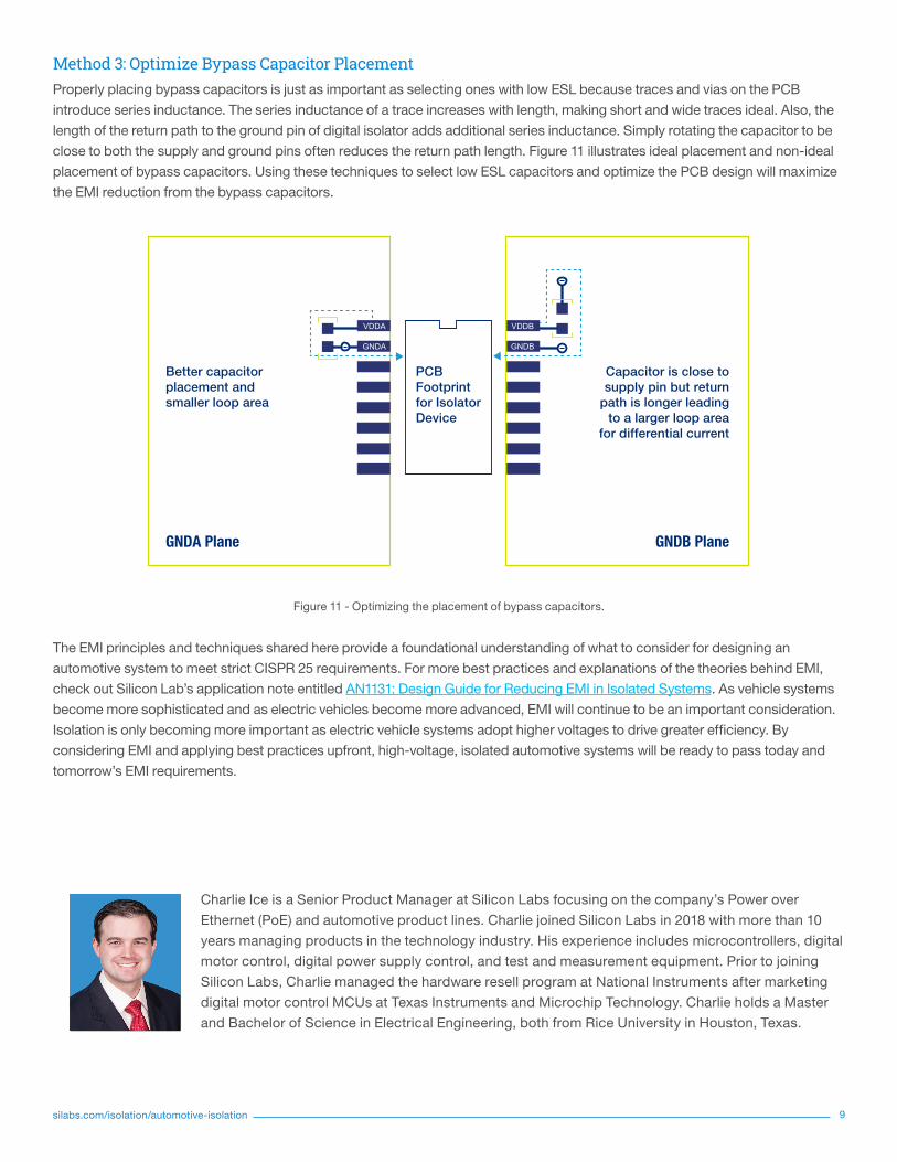
Properly placing bypass capacitors is just as important as selecting ones with low ESL because traces and vias on the PCB
introduce series inductance. The series inductance of a trace increases with length, making short and wide traces ideal. Also, the
length of the return path to the ground pin of digital isolator adds additional series inductance. Simply rotating the capacitor to be
close to both the supply and ground pins often reduces the return path length. Figure 11 illustrates ideal placement and non-ideal
placement of bypass capacitors. Using these techniques to select low ESL capacitors and optimize the PCB design will maximize
the EMI reduction from the bypass capacitors.
The EMI principles and techniques shared here provide a foundational understanding of what to consider for designing an
automotive system to meet strict CISPR 25 requirements. For more best practices and explanations of the theories behind EMI,
check out Silicon Lab’s application note entitled AN1131: Design Guide for Reducing EMI in Isolated Systems. As vehicle systems
become more sophisticated and as electric vehicles become more advanced, EMI will continue to be an important consideration.
Isolation is only becoming more important as electric vehicle systems adopt higher voltages to drive greater efficiency. By
considering EMI and applying best practices upfront, high-voltage, isolated automotive systems will be ready to pass today and
tomorrow’s EMI requirements.
Method 3: Optimize Bypass Capacitor Placement
GNDA Plane GNDB Plane
Better capacitorplacement andsmaller loop area
PCB Footprint for Isolator Device
Capacitor is close tosupply pin but return
path is longer leadingto a larger loop area
for differential current
VDDA
GNDA
VDDB
GNDB
Figure 11 - Optimizing the placement of bypass capacitors.
Charlie Ice is a Senior Product Manager at Silicon Labs focusing on the company’s Power over
Ethernet (PoE) and automotive product lines. Charlie joined Silicon Labs in 2018 with more than 10
years managing products in the technology industry. His experience includes microcontrollers, digital
motor control, digital power supply control, and test and measurement equipment. Prior to joining
Silicon Labs, Charlie managed the hardware resell program at National Instruments after marketing
digital motor control MCUs at Texas Instruments and Microchip Technology. Charlie holds a Master
and Bachelor of Science in Electrical Engineering, both from Rice University in Houston, Texas.