how to use the ntag i²c plus for bidirectional communication · nxp semiconductors an11579 how to...
TRANSCRIPT
AN11579 How to use the NTAG I²C plus for bidirectional communication Rev. 1.1 — 2 June 2018 302011
Application note COMPANY PUBLIC
Document information Info Content Keywords NTAG I2C plus, pass-through mode, bidirectional communication, SRAM
Abstract This document describes the various data communication modes the NTAG I²C plus provides. Especially it is about the SRAM-based pass-through mode and also how to synchronize data transfer through the NTAG I²C plus in general.
NXP Semiconductors AN11579 How to use the NTAG I²C plus for bidirectional communication
AN11579 All information provided in this document is subject to legal disclaimers. © NXP B.V. 2018. All rights reserved.
Application note COMPANY PUBLIC
Rev. 1.1 — 2 June 2018 302011
2 of 12
Contact information For more information, please visit: http://www.nxp.com
Revision history Rev Date Description 1.1 20180605 Editorial update and clarification on I²C address added
1.0 20160201 First release
NXP Semiconductors AN11579 How to use the NTAG I²C plus for bidirectional communication
AN11579 All information provided in this document is subject to legal disclaimers. © NXP B.V. 2018. All rights reserved.
Application note COMPANY PUBLIC
Rev. 1.1 — 2 June 2018 302011
3 of 12
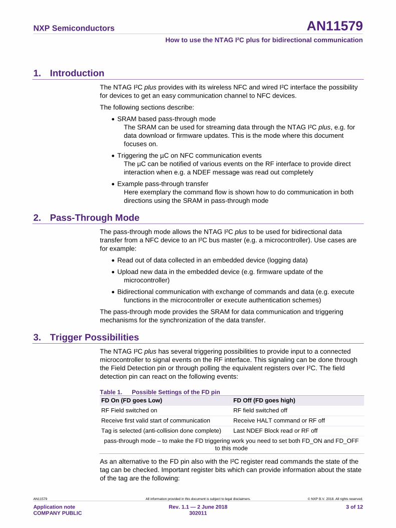
1. Introduction The NTAG I²C plus provides with its wireless NFC and wired I²C interface the possibility for devices to get an easy communication channel to NFC devices.
The following sections describe:
• SRAM based pass-through mode The SRAM can be used for streaming data through the NTAG I²C plus, e.g. for data download or firmware updates. This is the mode where this document focuses on.
• Triggering the µC on NFC communication events The µC can be notified of various events on the RF interface to provide direct interaction when e.g. a NDEF message was read out completely
• Example pass-through transfer Here exemplary the command flow is shown how to do communication in both directions using the SRAM in pass-through mode
2. Pass-Through Mode The pass-through mode allows the NTAG I²C plus to be used for bidirectional data transfer from a NFC device to an I²C bus master (e.g. a microcontroller). Use cases are for example:
• Read out of data collected in an embedded device (logging data)
• Upload new data in the embedded device (e.g. firmware update of the microcontroller)
• Bidirectional communication with exchange of commands and data (e.g. execute functions in the microcontroller or execute authentication schemes)
The pass-through mode provides the SRAM for data communication and triggering mechanisms for the synchronization of the data transfer.
3. Trigger Possibilities The NTAG I²C plus has several triggering possibilities to provide input to a connected microcontroller to signal events on the RF interface. This signaling can be done through the Field Detection pin or through polling the equivalent registers over I²C. The field detection pin can react on the following events:
Table 1. Possible Settings of the FD pin FD On (FD goes Low) FD Off (FD goes high) RF Field switched on RF field switched off
Receive first valid start of communication Receive HALT command or RF off
Tag is selected (anti-collision done complete) Last NDEF Block read or RF off
pass-through mode – to make the FD triggering work you need to set both FD_ON and FD_OFF to this mode
As an alternative to the FD pin also with the I²C register read commands the state of the tag can be checked. Important register bits which can provide information about the state of the tag are the following:
NXP Semiconductors AN11579 How to use the NTAG I²C plus for bidirectional communication
AN11579 All information provided in this document is subject to legal disclaimers. © NXP B.V. 2018. All rights reserved.
Application note COMPANY PUBLIC
Rev. 1.1 — 2 June 2018 302011
4 of 12
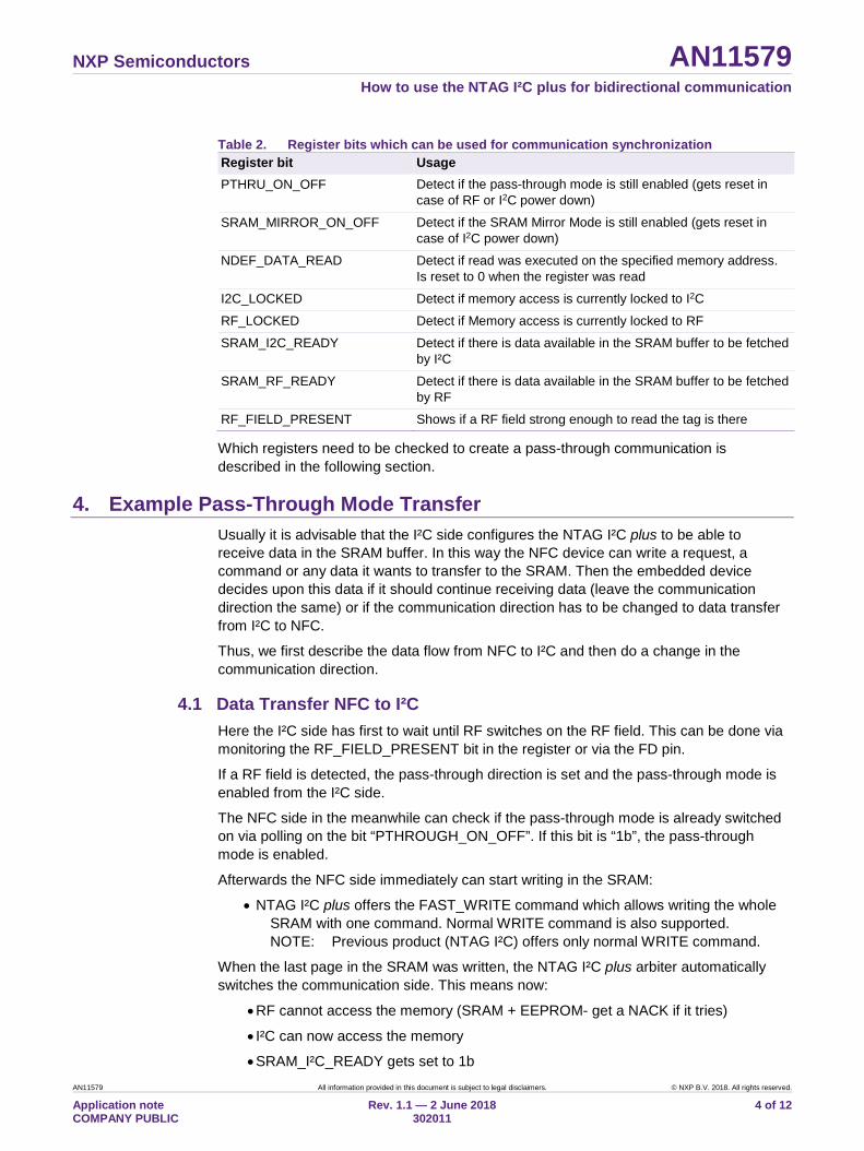
Table 2. Register bits which can be used for communication synchronization Register bit Usage PTHRU_ON_OFF Detect if the pass-through mode is still enabled (gets reset in
case of RF or I2C power down)
SRAM_MIRROR_ON_OFF Detect if the SRAM Mirror Mode is still enabled (gets reset in case of I2C power down)
NDEF_DATA_READ Detect if read was executed on the specified memory address. Is reset to 0 when the register was read
I2C_LOCKED Detect if memory access is currently locked to I2C
RF_LOCKED Detect if Memory access is currently locked to RF
SRAM_I2C_READY Detect if there is data available in the SRAM buffer to be fetched by I²C
SRAM_RF_READY Detect if there is data available in the SRAM buffer to be fetched by RF
RF_FIELD_PRESENT Shows if a RF field strong enough to read the tag is there
Which registers need to be checked to create a pass-through communication is described in the following section.
4. Example Pass-Through Mode Transfer Usually it is advisable that the I²C side configures the NTAG I²C plus to be able to receive data in the SRAM buffer. In this way the NFC device can write a request, a command or any data it wants to transfer to the SRAM. Then the embedded device decides upon this data if it should continue receiving data (leave the communication direction the same) or if the communication direction has to be changed to data transfer from I²C to NFC.
Thus, we first describe the data flow from NFC to I²C and then do a change in the communication direction.
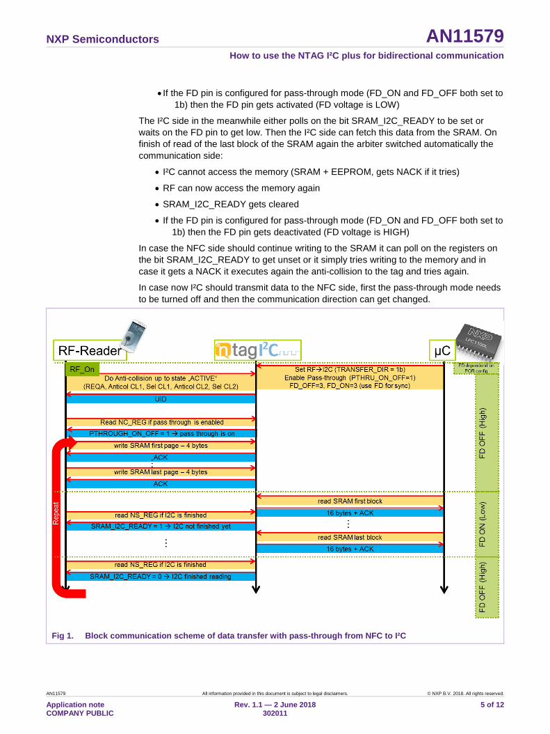
4.1 Data Transfer NFC to I²C Here the I²C side has first to wait until RF switches on the RF field. This can be done via monitoring the RF_FIELD_PRESENT bit in the register or via the FD pin.
If a RF field is detected, the pass-through direction is set and the pass-through mode is enabled from the I²C side.
The NFC side in the meanwhile can check if the pass-through mode is already switched on via polling on the bit “PTHROUGH_ON_OFF”. If this bit is “1b”, the pass-through mode is enabled.
Afterwards the NFC side immediately can start writing in the SRAM:
• NTAG I²C plus offers the FAST_WRITE command which allows writing the whole SRAM with one command. Normal WRITE command is also supported. NOTE: Previous product (NTAG I²C) offers only normal WRITE command.
When the last page in the SRAM was written, the NTAG I²C plus arbiter automatically switches the communication side. This means now:
• RF cannot access the memory (SRAM + EEPROM- get a NACK if it tries)
• I²C can now access the memory
• SRAM_I²C_READY gets set to 1b
NXP Semiconductors AN11579 How to use the NTAG I²C plus for bidirectional communication
AN11579 All information provided in this document is subject to legal disclaimers. © NXP B.V. 2018. All rights reserved.
Application note COMPANY PUBLIC
Rev. 1.1 — 2 June 2018 302011
5 of 12
• If the FD pin is configured for pass-through mode (FD_ON and FD_OFF both set to 1b) then the FD pin gets activated (FD voltage is LOW)
The I²C side in the meanwhile either polls on the bit SRAM_I2C_READY to be set or waits on the FD pin to get low. Then the I²C side can fetch this data from the SRAM. On finish of read of the last block of the SRAM again the arbiter switched automatically the communication side:
• I²C cannot access the memory (SRAM + EEPROM, gets NACK if it tries)
• RF can now access the memory again
• SRAM_I2C_READY gets cleared
• If the FD pin is configured for pass-through mode (FD_ON and FD_OFF both set to 1b) then the FD pin gets deactivated (FD voltage is HIGH)
In case the NFC side should continue writing to the SRAM it can poll on the registers on the bit SRAM_I2C_READY to get unset or it simply tries writing to the memory and in case it gets a NACK it executes again the anti-collision to the tag and tries again.
In case now I²C should transmit data to the NFC side, first the pass-through mode needs to be turned off and then the communication direction can get changed.
Fig 1. Block communication scheme of data transfer with pass-through from NFC to I²C
NXP Semiconductors AN11579 How to use the NTAG I²C plus for bidirectional communication
AN11579 All information provided in this document is subject to legal disclaimers. © NXP B.V. 2018. All rights reserved.
Application note COMPANY PUBLIC
Rev. 1.1 — 2 June 2018 302011
6 of 12
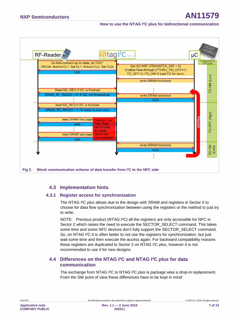
4.2 Data Transfer from I²C to NFC If I²C needs to transfer data to the NFC side, also here first both sides need to be powered. This can be done via monitoring the RF_FIELD_PRESENT bit in the register or via the FD pin.
If a RF field is detected, the pass-through direction is set and the pass-through mode is enabled from the I²C side.
In this communication direction the I²C side can immediately start writing data in the SRAM buffer. When the write of the last block of the SRAM buffer has finished, the NTAG I²C plus arbiter automatically switched the communication sides:
• I²C cannot access the memory (SRAM and EEPROM, gets NACK if it tries)
• RF can now access the memory again
• SRAM_RF_READY gets set
• If the FD pin is configured for pass-through mode (FD_ON and FD_OFF both set to 1b) then the FD pin gets deactivated (FD voltage is HIGH)
The NFC side in the meanwhile can check if data is already available in the SRAM via polling on the bit “SRAM_RF_READY” or it simply tries reading the memory and in case it gets a NACK it executes again the anti-collision to the tag and tries again.
Afterwards the NFC side can read the SRAM. This best is done using the “FAST_READ” command which allows reading the whole SRAM with one command. When the last page in the SRAM was read, the NTAG I²C plus arbiter automatically switches the communication side. This means now:
• RF cannot access the memory (SRAM and EEPROM- get a NACK if it tries)
• I²C can now access the memory
• SRAM_RF_READY gets reset
• If the FD pin is configured for pass-through mode (FD_ON and FD_OFF both set to 1b) then the FD pin gets activated (FD voltage is LOW)
The I²C side either can poll on the bit SRAM_RF_READY in the registers or listen on the FD pin to get low. Afterwards it can either write new data in the SRAM or switch the data flow direction via turning the pass-through mode off first, switch the direction and then turn it on again.
NXP Semiconductors AN11579 How to use the NTAG I²C plus for bidirectional communication
AN11579 All information provided in this document is subject to legal disclaimers. © NXP B.V. 2018. All rights reserved.
Application note COMPANY PUBLIC
Rev. 1.1 — 2 June 2018 302011
7 of 12
Fig 2. Block communication scheme of data transfer from I²C to the NFC side
4.3 Implementation hints 4.3.1 Register access for synchronization
The NTAG I²C plus allows due to the design with SRAM and registers in Sector 0 to choose for data flow synchronization between using the registers or the method to just try to write.
NOTE: Previous product (NTAG I²C) all the registers are only accessible for NFC in Sector 2 which raises the need to execute the SECTOR_SELECT command. This takes some time and some NFC devices don’t fully support the SECTOR_SELECT command. So, on NTAG I²C it is often better to not use the registers for synchronization, but just wait some time and then execute the access again. For backward compatibility reasons these registers are duplicated to Sector 2 on NTAG I²C plus, however it is not recommended to use it for new designs.
4.4 Differences on the NTAG I²C and NTAG I²C plus for data communication The exchange from NTAG I²C to NTAG I²C plus is package wise a drop-in replacement. From the SW point of view these differences have to be kept in mind:
NXP Semiconductors AN11579 How to use the NTAG I²C plus for bidirectional communication
AN11579 All information provided in this document is subject to legal disclaimers. © NXP B.V. 2018. All rights reserved.
Application note COMPANY PUBLIC
Rev. 1.1 — 2 June 2018 302011
8 of 12
• GET_VERSION response To identify the four different types (memory size 1K and 2K, NTAG I²C and NTAG I²C plus), each NTAG I²C model has its own GET_VERSION response
• SRAM location as seen from NFC side The NTAG I²C plus has the SRAM now on the 1k and 2k memory size at the same location as the NTAG I²C 1k to enhance compatibility.
• Register access from NFC The set of registers on the NTAG I²C is on Sector 2, whereas in the NTAG I²C plus it is additionally duplicated in Sector 0. So, there is no need for a change, but the change is recommended as it increases compatibility.
• NDEF memory size User switching from the NTAG I²C 2k and using NDEF messages not fitting in the Sector 1 has to include the memory control TLV like described in the datasheet.
• Default Memory initialization The NTAG I²C plus is by default not NDEF formatted to increase the configuration flexibility. Before a NDEF message can be written to the tag the pages 03 and 04 have to be initialized like exemplary described in the datasheet.
NOTE: When configuring Block 0 of NTAG I²C plus from I²C perspective, also I²C write address gets updated, because I²C write address is stored in the first byte of user memory. Reading out this first byte of NTAG I²C plus, it always returns 04h (UID0). Therefore, for convenience reasons, it is recommended to change default I²C device address 55h to 02h. As this first byte codes I²C write address, 04h (02h shifted left by one bit) value needs to be written to Byte 0.
NXP Semiconductors AN11579 How to use the NTAG I²C plus for bidirectional communication
AN11579 All information provided in this document is subject to legal disclaimers. © NXP B.V. 2018. All rights reserved.
Application note COMPANY PUBLIC
Rev. 1.1 — 2 June 2018 302011
9 of 12
5. Legal information
5.1 Definitions Draft — The document is a draft version only. The content is still under internal review and subject to formal approval, which may result in modifications or additions. NXP Semiconductors does not give any representations or warranties as to the accuracy or completeness of information included herein and shall have no liability for the consequences of use of such information.
5.2 Disclaimers Limited warranty and liability — Information in this document is believed to be accurate and reliable. However, NXP Semiconductors does not give any representations or warranties, expressed or implied, as to the accuracy or completeness of such information and shall have no liability for the consequences of use of such information. NXP Semiconductors takes no responsibility for the content in this document if provided by an information source outside of NXP Semiconductors.
In no event shall NXP Semiconductors be liable for any indirect, incidental, punitive, special or consequential damages (including - without limitation - lost profits, lost savings, business interruption, costs related to the removal or replacement of any products or rework charges) whether or not such damages are based on tort (including negligence), warranty, breach of contract or any other legal theory.
Notwithstanding any damages that customer might incur for any reason whatsoever, NXP Semiconductors’ aggregate and cumulative liability towards customer for the products described herein shall be limited in accordance with the Terms and conditions of commercial sale of NXP Semiconductors.
Right to make changes — NXP Semiconductors reserves the right to make changes to information published in this document, including without limitation specifications and product descriptions, at any time and without notice. This document supersedes and replaces all information supplied prior to the publication hereof.
Suitability for use — NXP Semiconductors products are not designed, authorized or warranted to be suitable for use in life support, life-critical or safety-critical systems or equipment, nor in applications where failure or malfunction of an NXP Semiconductors product can reasonably be expected to result in personal injury, death or severe property or environmental damage. NXP Semiconductors and its suppliers accept no liability for inclusion and/or use of NXP Semiconductors products in such equipment or applications and therefore such inclusion and/or use is at the customer’s own risk.
Applications — Applications that are described herein for any of these products are for illustrative purposes only. NXP Semiconductors makes no representation or warranty that such applications will be suitable for the specified use without further testing or modification.
Customers are responsible for the design and operation of their applications and products using NXP Semiconductors products, and NXP Semiconductors accepts no liability for any assistance with applications or customer product design. It is customer’s sole responsibility to determine whether the NXP Semiconductors product is suitable and fit for the customer’s applications and products planned, as well as for the planned application and use of customer’s third party customer(s). Customers should provide appropriate design and operating safeguards to minimize the risks associated with their applications and products.
NXP Semiconductors does not accept any liability related to any default, damage, costs or problem which is based on any weakness or default in the customer’s applications or products, or the application or use by customer’s third party customer(s). Customer is responsible for doing all necessary testing for the customer’s applications and products using NXP Semiconductors products in order to avoid a default of the applications and the products or of the application or use by customer’s third party customer(s). NXP does not accept any liability in this respect.
Export control — This document as well as the item(s) described herein may be subject to export control regulations. Export might require a prior authorization from competent authorities.
Translations — A non-English (translated) version of a document is for reference only. The English version shall prevail in case of any discrepancy between the translated and English versions.
Evaluation products — This product is provided on an “as is” and “with all faults” basis for evaluation purposes only. NXP Semiconductors, its affiliates and their suppliers expressly disclaim all warranties, whether express, implied or statutory, including but not limited to the implied warranties of non-infringement, merchantability and fitness for a particular purpose. The entire risk as to the quality, or arising out of the use or performance, of this product remains with customer.
In no event shall NXP Semiconductors, its affiliates or their suppliers be liable to customer for any special, indirect, consequential, punitive or incidental damages (including without limitation damages for loss of business, business interruption, loss of use, loss of data or information, and the like) arising out the use of or inability to use the product, whether or not based on tort (including negligence), strict liability, breach of contract, breach of warranty or any other theory, even if advised of the possibility of such damages.
Notwithstanding any damages that customer might incur for any reason whatsoever (including without limitation, all damages referenced above and all direct or general damages), the entire liability of NXP Semiconductors, its affiliates and their suppliers and customer’s exclusive remedy for all of the foregoing shall be limited to actual damages incurred by customer based on reasonable reliance up to the greater of the amount actually paid by customer for the product or five dollars (US$5.00). The foregoing limitations, exclusions and disclaimers shall apply to the maximum extent permitted by applicable law, even if any remedy fails of its essential purpose.
5.3 Licenses Purchase of NXP ICs with NFC technology
Purchase of an NXP Semiconductors IC that complies with one of the Near Field Communication (NFC) standards ISO/IEC 18092 and ISO/IEC 21481 does not convey an implied license under any patent right infringed by implementation of any of those standards. Purchase of NXP Semiconductors IC does not include a license to any NXP patent (or other IP right) covering combinations of those products with other products, whether hardware or software.
5.4 Trademarks Notice: All referenced brands, product names, service names and trademarks are property of their respective owners.
NTAG — is a trademark of NXP B.V
I²C-bus — logo is a trademark of NXP B.V
NXP Semiconductors AN11579 How to use the NTAG I²C plus for bidirectional communication
AN11579 All information provided in this document is subject to legal disclaimers. © NXP B.V. 2018. All rights reserved.
Application note COMPANY PUBLIC
Rev. 1.1 — 2 June 2018 302011
10 of 12
6. List of figures
Fig 1. Block communication scheme of data transfer with pass-through from NFC to I²C ................... 5
Fig 2. Block communication scheme of data transfer from I²C to the NFC side ................................... 7
NXP Semiconductors AN11579 How to use the NTAG I²C plus for bidirectional communication
AN11579 All information provided in this document is subject to legal disclaimers. © NXP B.V. 2018. All rights reserved.
Application note COMPANY PUBLIC
Rev. 1.1 — 2 June 2018 302011
11 of 12
7. List of tables
Table 1. Possible Settings of the FD pin ......................... 3 Table 2. Register bits which can be used for
communication synchronization ........................ 4
NXP Semiconductors AN11579 How to use the NTAG I²C plus for bidirectional communication
Please be aware that important notices concerning this document and the product(s) described herein, have been included in the section 'Legal information'.
© NXP B.V. 2018. All rights reserved.
For more information, visit: http://www.nxp.com For sales office addresses, please send an email to: [email protected]
Date of release: 2 June 2018 302011 Document identifier: AN11579
8. Contents
1. Introduction ......................................................... 3 2. Pass-Through Mode ............................................ 3 3. Trigger Possibilities ............................................ 3 4. Example Pass-Through Mode Transfer ............. 4 4.1 Data Transfer NFC to I²C ................................... 4 4.2 Data Transfer from I²C to NFC ........................... 6 4.3 Implementation hints .......................................... 7 4.3.1 Register access for synchronization ................... 7 4.4 Differences on the NTAG I²C and NTAG I²C plus
for data communication ...................................... 7 5. Legal information ................................................ 9 5.1 Definitions .......................................................... 9 5.2 Disclaimers......................................................... 9 5.3 Licenses ............................................................. 9 5.4 Trademarks ........................................................ 9 6. List of figures ..................................................... 10 7. List of tables ...................................................... 11 8. Contents ............................................................. 12