hr c6000 user manual...56 u_sdi di mcu accesses hr_c6000 register or ram spi data input for the...
TRANSCRIPT
HR_C6000 User Manual
DISCLAIMERNO IMPLICIT OR EXPLICIT WARRANTY IS GIVEN WITHTHIS TRANSLATION. THE TRANSLATOR TAKES NORESPONSIBILITY FOR ANY INACCURACY OF THISDOCUMENT AND FOR ANY DAMAGE FOLLOWING ANINAPPROPRIATE USE OF THE DEVICES AND NOTFOLLOWING THE ORIGINAL MANUFACTURERINSTRUCTIONS. IF YOU DON’T UNDERSTANDSOMETHING, LOOK AT THE ORIGINAL DOCUMENT ANDASK SOMEONE TO TRANSLATE IT FOR YOU.
This version: 0.2

CharacteristicsDMR
• Protocol design in accordance with ETSI TS102 361 (DMR) Tier I/II/III standard• Support physical layer, data link layer and call control layer independent control• Support true dual-slot sync header detection• Supports full-duplex, half-duplex voice, data communication and simultaneous digital
messaging services using TDMA technology• Support IP data services• Support single frequency, dual frequency relay• Support 4.8Kbps and 9.6Kbps data transmission• Support digital-analog intelligent detection• Support for relay voice and data functions• Support voice encryption
Modem and channel codec• High performance 4FSK modem• Channel codec specified by the integration protocol
Vocoder support• Support HR_V3000 (Hongrui AMBE+2), SELP vocoder (Tsinghua), AVDS vocoder (712)• Wait for the SPI interface vocoder to provide an interface for digital recording, playback and
prompt input• Seamless docking AMBE3000, AMBE1000, WT3000 and other vocoders, automatically by
HR_C6000• Complete the configuration of the vocoder and control the data exchanged with the vocoder• Support for digital voice encryption
RF interface• Transmit RF interface with single-ended output, support baseband IQ, intermediate
frequency, two-point modulation• Receive RF interface with differential input, supporting baseband IQ, IF and AF• Send two signal offsets, the amplitude can be adjusted independently• Support user configuration GPIO control RF channel
Analog FM• Support 12.5KHz/25KHz channel communication• Support aggravation, de-emphasis• Support compression, decompression• Support CDCSS/CTCSS sub-tone processing• Support 2-tone/5-tone processing• Support for DTMF processing• Support for analog squelch• Support MSK modulation and demodulation
Built-in high performance IP• High performance ADC/DAC• DC-DC, powered by 3.3V• High performance PLL• High-performance Codec with differential or single-ended Mic input and Line_out output• Support for external Codec 2 I S interface• With low power design, the typical power consumption of the chip is less than 40mW• Available in LQFP-80 package
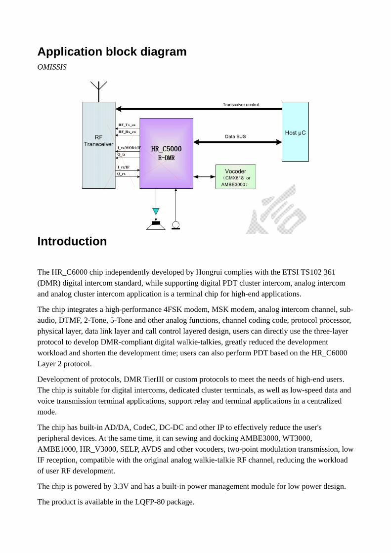
Application block diagramOMISSIS
Introduction
The HR_C6000 chip independently developed by Hongrui complies with the ETSI TS102 361 (DMR) digital intercom standard, while supporting digital PDT cluster intercom, analog intercom and analog cluster intercom application is a terminal chip for high-end applications.
The chip integrates a high-performance 4FSK modem, MSK modem, analog intercom channel, sub-audio, DTMF, 2-Tone, 5-Tone and other analog functions, channel coding code, protocol processor, physical layer, data link layer and call control layered design, users can directly use the three-layer protocol to develop DMR-compliant digital walkie-talkies, greatly reduced the development workload and shorten the development time; users can also perform PDT based on the HR_C6000 Layer 2 protocol.
Development of protocols, DMR TierIII or custom protocols to meet the needs of high-end users. The chip is suitable for digital intercoms, dedicated cluster terminals, as well as low-speed data and voice transmission terminal applications, support relay and terminal applications in a centralized mode.
The chip has built-in AD/DA, CodeC, DC-DC and other IP to effectively reduce the user's peripheral devices. At the same time, it can sewing and docking AMBE3000, WT3000, AMBE1000, HR_V3000, SELP, AVDS and other vocoders, two-point modulation transmission, lowIF reception, compatible with the original analog walkie-talkie RF channel, reducing the workload of user RF development.
The chip is powered by 3.3V and has a built-in power management module for low power design.
The product is available in the LQFP-80 package.
Table of ContentsCharacteristics......................................................................................................................................2Application block diagram...................................................................................................................3Introduction..........................................................................................................................................31Chip block diagram............................................................................................................................52Chip pin..............................................................................................................................................6
2.1Pin map.......................................................................................................................................62.2Pin list.........................................................................................................................................72.3Package size..............................................................................................................................11
3Chip characteristic............................................................................................................................113.1Static characteristic...................................................................................................................113.2Dynamic characteristics............................................................................................................113.3Power consumption parameter..................................................................................................113.4Performance parameter.............................................................................................................11
4Application note...............................................................................................................................124.1Chip reset..................................................................................................................................12
4.1.1Power-on reset...................................................................................................................124.1.2Software reset....................................................................................................................12
4.2Chip power supply....................................................................................................................124.3Chip working clock block diagram and description.................................................................13
4.3.1Clock circuit......................................................................................................................134.3.2Clock configuration...........................................................................................................13
4.4Chip parameter configuration interface....................................................................................144.5Use of Codec.............................................................................................................................17
4.5.1Built-in Codec...................................................................................................................174.5.2Use external Codec...........................................................................................................17
4.6Vocoder.....................................................................................................................................184.6.1Interface definition with Hongrui HR_V3000 vocoder....................................................18
4.7Transmitter module...................................................................................................................204.7.1Baseband IQ modulation...................................................................................................214.7.2Two-point modulation.......................................................................................................214.7.3IF IQ modulation...............................................................................................................214.7.4IF modulation....................................................................................................................21
4.8Receiving module.....................................................................................................................214.8.1Baseband IQ......................................................................................................................214.8.2IF mode.............................................................................................................................21
5Hierarchical function description.....................................................................................................215.1Interrupt use instructions..........................................................................................................22
5.1.1Interrupt use description....................................................................................................225.2Interface read and write instructions.........................................................................................255.3HR_C6000 RAM allocation definition.....................................................................................265.4Support frame type....................................................................................................................28
5.4.1Time slot framing..............................................................................................................285.4.2Framing mode...................................................................................................................345.4.3Frame definition and use...................................................................................................345.4.4Working mode description................................................................................................365.4.5Application examples........................................................................................................405.4.6Bit error rate test...............................................................................................................42
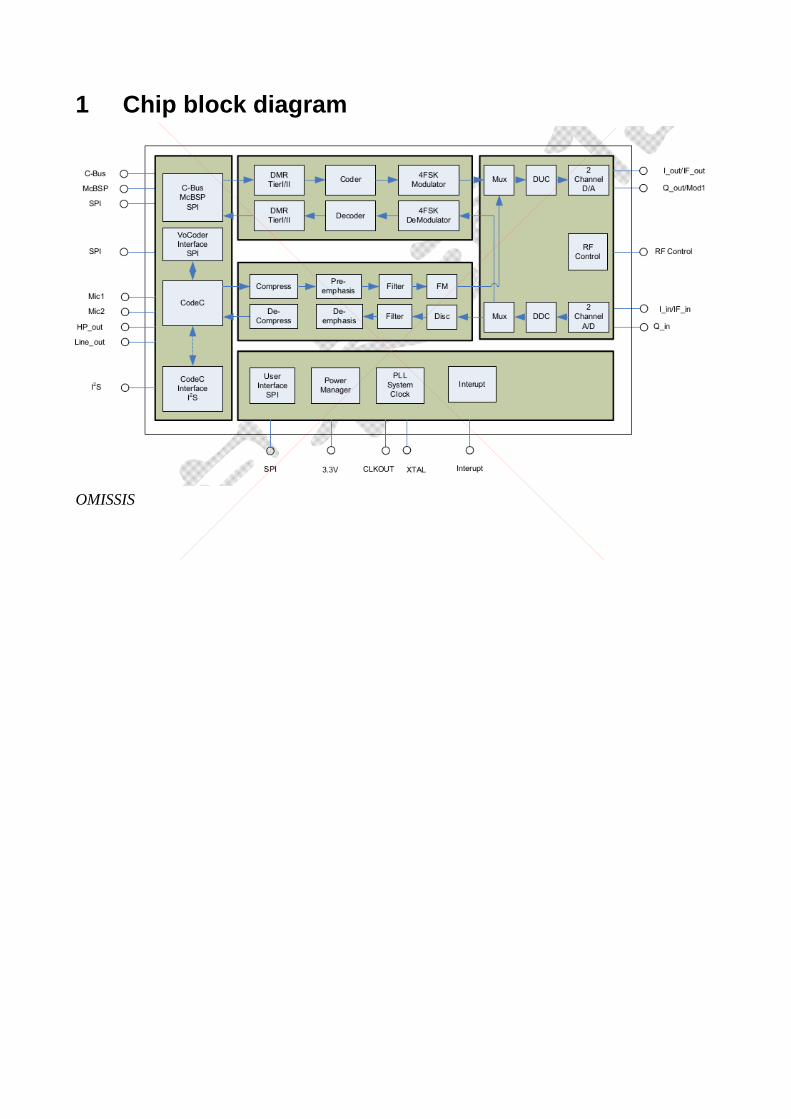
1 Chip block diagram
OMISSIS

2 Chip pin
2.1 Pin mapOMISSIS
HR_C6000 pin diagram picture is missing
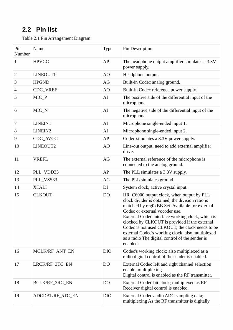
2.2 Pin listTable 2.1 Pin Arrangement Diagram
Pin Number
Name Type Pin Description
1 HPVCC AP The headphone output amplifier simulates a 3.3V power supply.
2 LINEOUT1 AO Headphone output.
3 HPGND AG Built-in Codec analog ground.
4 CDC_VREF AO Built-in Codec reference power supply.
5 MIC_P AI The positive side of the differential input of the microphone.
6 MIC_N AI The negative side of the differential input of the microphone.
7 LINEIN1 AI Microphone single-ended input 1.
8 LINEIN2 AI Microphone single-ended input 2.
9 CDC_AVCC AP Codec simulates a 3.3V power supply.
10 LINEOUT2 AO Line-out output, need to add external amplifier drive.
11 VREFL AG The external reference of the microphone is connected to the analog ground.
12 PLL_VDD33 AP The PLL simulates a 3.3V supply.
13 PLL_VSS33 AG The PLL simulates ground.
14 XTALI DI System clock, active crystal input.
15 CLKOUT DO HR_C6000 output clock, when output by PLL clock divider is obtained, the division ratio is matched by reg0xBB Set. Available for external Codec or external vocoder use.External Codec interface working clock, which is clocked by CLKOUT is provided if the external Codec is not used CLKOUT, the clock needs to beexternal Codec's working clock; also multiplexed as a radio The digital control of the sender is enabled.
16 MCLK/RF_ANT_EN DIO Codec's working clock; also multiplexed as a radio digital control of the sender is enabled.
17 LRCK/RF_3TC_EN DO External Codec left and right channel selection enable; multiplexingDigital control is enabled as the RF transmitter.
18 BCLK/RF_3RC_EN DO External Codec bit clock; multiplexed as RFReceiver digital control is enabled.
19 ADCDAT/RF_5TC_EN DIO External Codec audio ADC sampling data; multiplexing As the RF transmitter is digitally

enabled, this time For output characteristics.
20 DACDAT/RF_5RC_EN DO External Codec audio DAC data; reuse asDigital control at the RF receiver is enabled.
21 VSS12 G The kernel is digitally ground.
22 McBSP_Rxd/CHS_DI DO AMBE3000: HR_C6000 by McBSPThe data sent by the interface to the AMBE3000;AMBE1000: HR_C6000 through CHS stringThe frame input data sent to the AMBE1000 by the port.
23 McBSP_TxD/CHS_DO DI AMBE3000: HR_C6000 by McBSPThe interface receives data sent by the AMBE3000;AMBE1000: HR_C6000 through CHS stringThe port receives the frame output data of the AMBE1000.
24 McBSP_CLKR/CHS_O_CLK DO AMBE3000: McBSP connection of HR_C6000Port output clock;AMBE1000: CHS interface clock of AMBE1000.
25 McBSP_FSX DI AMBE3000: HR_C6000 by McBSP Interface receives synchronization of AMBE3000 output data signal.
26 McBSP_CLKX DI AMBE3000: McBSP connection of HR_C6000 Port input clock.
27 McBSP_FSR/CHS_I_STRB DO AMBE3000: HR_C6000 by McBSP The data synchronization letter sent by the interface to the AMBE3000 number;AMBE1000: CHS_DI port data is valid Enable.
28 PKT_RX_WAKE/CHS_O_STRB DO AMBE3000: Invert McBSP_FSR, Used to wake up the McBSP interface;AMBE1000: CHS_DO port data is valid Enablement.
29 RTS/DPE DI AMBE3000 : AMBE3000 is allowed to passThe McBsp interface writes data, which is low effective;AMBE1000: AMBE1000 decoding packet is empty.
30 TX_RDY/EPR DI AMBE3000: AMBE3000 sends a packet Ready tocomplete, high effective; MBE1000: AMBE1000 encoding standard Ready.
31 STDB_ENB/RESET_AMBE1000 AMBE3000: AMBE3000 Standby Mode Enable, active high;AMBE1000: AMBE1000 RESET, Low effective.
32 VDD12 P Core digital 1.2V power supply.
33 VSS12 G The kernel is digitally ground.
34 (C_SDI/I2S_RX) – supposed DI As an SPI interface: the vocoder SPI port Serial data input to HR_C6000, SPI operation In the

main mode.
35 C_SDO/I2S_TX DO As an I2S interface: can work in master/slave mode formula. If working in master mode, read from the vocoder Take PCM serial data to HR_C6000; if Working in slave mode, the vocoder will write PCM data Go to HR_C6000.As an SPI interface: HR_C6000 will Output voice data from CodecADC to vocoding SPI port.
36 C_SCLK/I2S_CK DO/DI As an I2S interface: can work in master/slave mode formula. If working in master mode, if working in Main mode, the I2S master that is provided to the vocoder Clock; if working in slavemode, for vocoder When working with the I2S interface of the HR_C6000 bell As an SPI interface: a slice of the vocoder SPI port selected.
37 C_CS/I2S_FS DO/DI As an I2S interface: can work in master/slave mode formula. If working in master mode, provide vocoding Read and write I2S left and right channel data enable; Fruit work is provided from the mode, the vocoder HR_C6000 reads and writes the left and right channels of serial dataEnable.
38 TEST_MODE DI Test mode configuration pin, 1 is test mode, 0 for normal working mode.
39 RESETn DI System reset signal, active low.
40 VSS33 P Digital IO 3.3V power supply.
41 V_SDI DI Universal vocoder SPI port serial data input.
42 V_SDO DO Universal vocoder SPI port serial data output.
43 V_SCLK DI Universal vocoder SPI port serial clock.
44 V_CS DI Universal vocoder SPI port chip select
45 DBIST_IN DI NC. Connect to ground.
46 DBIST_OUT DO NC
47 PWD DI Chip PowerDown control pin, high level activates the PowerDown state.
48 TIME_SLOT_INTER DO 30ms time slot interrupt.
49 SYS_INTER DO System control is interrupted.
50 DO The radio end sends related parameters to configure interrupts, such as sending the mixer frequency configuration.
51 DO The radio end receives the relevant parameter configuration interrupt, such as receive the mixer frequency configuration.
52 VSS12 G The kernel is digitally ground.
53 VDD12 P Core digital 1.2V power supply.

54 VDD33 P Digital IO 3.3V power supply.
55 U_SDO DO MCU accesses HR_C6000 register or RAMSPI data output from the memory area.
56 U_SDI DI MCU accesses HR_C6000 register or RAMSPI data input for the bank.
57 U_SCLK DI MCU accesses HR_C6000 register or RAMThe SPI serial clock for the bank.
58 U_CS DI MCU accesses HR_C6000 register or RAMSPI chip select for the bank.
59 RF_RX_EN DO Control the RF receiving switch to enable, when receiving status,Output high level. The signal will not beRF_TX_EN is valid at the same time.
60 RF_TX_EN DO Control the RF transmit switch enable, when sending status,Output high level. The signal will not beRF_RX_EN is valid at the same time.
61 ADC_VBG_Q AIO Q-channel ADC channel external decoupling bandgap voltage
62 ADC_QVINN AI Q The negative side of the ADC channel differential input.
63 ADC_QVINP AI Q Positive side of the ADC channel differential input.
64 ADC_AVDD12_Q AP The Q-channel ADC channel simulates a 1.2V power supply.
65 ADC_AGND_Q AG Q-channel ADC channel analog ground.
66 ADC_AVDD33_Q AP ADC Analog 3.3V Power Supply
67 ADC_AVDD33_I AP ADC Analog 3.3V Power Supply
68 ADC_AGND_I AG I-channel ADC channel analog ground
69 ADC_AVDD12_I AP The I-channel ADC channel simulates a 1.2V power supply.
70 ADC_IVINP AI I-channel ADC channel differential input positive terminal, or mediumSignal access terminal in frequency receiving mode.
71 ADC_IVINN I-channel ADC channel differential input negative terminal, intermediate frequency.The port is grounded or other fixed in receive modePressure.
72 ADC_VBG_I The bandgap voltage of the external decoupling ofthe I-channel ADC channel.
73 DAC_AVSS33 AG The DAC simulates ground.
74 DAC_QVOUT/MOD2 AO Q channel DAC channel output signal.
Two-point modulation MOD2 port in send mode.
75 DAC_IVOUT/MOD1 AO I DAC channel output signal.MOD1 port in two-point modulation transmit mode.
76 DAC_AVDD33 AP The DAC simulates a 3.3V power supply.
77 DCDC_VDD12 AO DC-DC 1.2V output.
78 DCDC_VSS G DC-DC digital ground.
79 DCDC_VDD33 P DC-DC 3.3V power supply.
80 DCDC_SW O DC-DC internal switch.
2.3 Package sizeOMISSIS
3 Chip characteristic
3.1 Static characteristicTable 3.1 HR_C6000 Static Parameters
OMISSIS
3.2 Dynamic characteristics
OMISSIS
3.3 Power consumption parameter
OMISSIS
3.4 Performance parameter
OMISSIS
4 Application note
4.1 Chip reset
4.1.1 Power-on reset
The HR_C6000 can be powered on and reset using resistors and capacitors. The reference circuit is as follows.
OMISSIS
Figure 4.1 Chip Power-on Reset Reference Circuit
To ensure a successful power-on reset, the reset time is required to be kept to a minimum of 0.1μs. s. As shown, 0-0.8V is stable low power flat voltage range, 2.0-3.3V is a stable high-level voltage range.
OMISSIS
Figure 4.2 Chip power-on reset timing diagram
It is recommended to use the same reset chip as the CPU or the GPIO of the CPU as the reset pin.
4.1.2 Software reset
In addition to the automatic reset process during power-on, the HR_C6000 can also pass the MCU according to the actual application needs.
Software reset the chip. The software reset operation is implemented by Bit7 of the configuration register Reg0x00. Will be Reg0x00
After Bit7 is configured as 0, a soft reset of HR_C6000 is completed, and the reset time is a Sys_Clk pulse width, that is, 1/9.8304 uS. After this bit is configured as 0, it is not necessary to reconfigure to 1 to resume normal operation mode through the MCU. The HR_C6000 automaticallysets Bit to 1.
OMISSIS
Figure 4.3 Chip Software Reset Timing Diagram
4.2 Chip power supplyThe HR_C6000 requires 3.3V power supply and the built-in DCDC module outputs 1.2V for digitaland analog cores. By outside The circuit separates the analog 3.3V, digital 3.3V and analog 1.2V, digital 1.2V power supplies. Digital 1.2V and digital 3.3V
The power supply shares digital ground; all analog 3.3V common ground; all analog 1.2V common ground.
The power supply network is shown in the figure, where VCC33 provides the total power supply for the system and AVDD33 is the chip to simulate the 3.3V power supply.
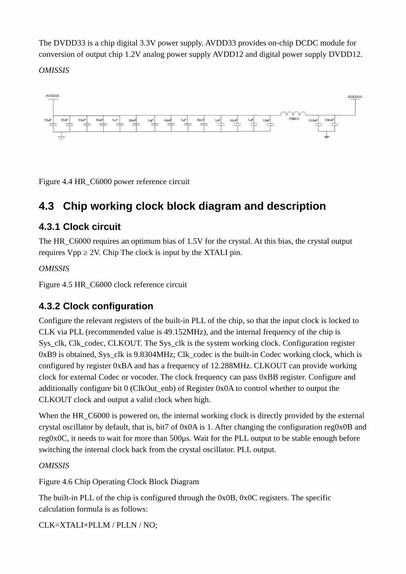
The DVDD33 is a chip digital 3.3V power supply. AVDD33 provides on-chip DCDC module for conversion of output chip 1.2V analog power supply AVDD12 and digital power supply DVDD12.
OMISSIS
Figure 4.4 HR_C6000 power reference circuit
4.3 Chip working clock block diagram and description
4.3.1 Clock circuit
The HR_C6000 requires an optimum bias of 1.5V for the crystal. At this bias, the crystal output requires Vpp ≥ 2V. Chip The clock is input by the XTALI pin.
OMISSIS
Figure 4.5 HR_C6000 clock reference circuit
4.3.2 Clock configuration
Configure the relevant registers of the built-in PLL of the chip, so that the input clock is locked to CLK via PLL (recommended value is 49.152MHz), and the internal frequency of the chip is Sys_clk, Clk_codec, CLKOUT. The Sys_clk is the system working clock. Configuration register 0xB9 is obtained, Sys_clk is 9.8304MHz; Clk_codec is the built-in Codec working clock, which is configured by register 0xBA and has a frequency of 12.288MHz. CLKOUT can provide working clock for external Codec or vocoder. The clock frequency can pass 0xBB register. Configure and additionally configure bit 0 (ClkOut_enb) of Register 0x0A to control whether to output the CLKOUT clock and output a valid clock when high.
When the HR_C6000 is powered on, the internal working clock is directly provided by the external crystal oscillator by default, that is, bit7 of 0x0A is 1. After changing the configuration reg0x0B andreg0x0C, it needs to wait for more than 500μs. s. Wait for the PLL output to be stable enough before switching the internal clock back from the crystal oscillator. PLL output.
OMISSIS
Figure 4.6 Chip Operating Clock Block Diagram
The built-in PLL of the chip is configured through the 0x0B, 0x0C registers. The specific calculation formula is as follows:
CLK=XTALI×PLLM / PLLN / NO;
among them:
NO=2 PLLDO
1M<XTAL/ PLLN<25MHz;
200MHz<CLK×NO<1000MHz;
PLLM>1;PLLN>1;
By setting bit 7 of the 0x0C register to 1, the PLL can be bypassed. At this time, the PLL output is CLK=XTALI;
Configure bit 0 of 0x0C to 1 or the PWD pin of the chip is pulled high to put the PLL into sleep state. At this time, the PLL has no clock output.
Configure bit 7 (Clk_in_sel) of Register 0x0A as 1, and CLK does not select the output clock of the PLL. Instead, choose XTALI directly, which is CLK=XTALI.
Table 4.1 recommends two typical PLL output clock configuration parameters
XTALI PLL configurationparameters
PLL outputclock
System clock configurationparameter
System output clock
12.288M Reg0x0B = 0x40 Reg0x0C = 0x32
49.152M Reg0xB9 = 0x05Reg0xBA = 0x04Reg0xBB = 0x02
Sys_clk=9.8304Clk_codec=12.288MCLKOUT=24.576M
29.4912M Reg0x0B = 0x28Reg0x0C = 0x33
49.152M Reg0xB9 = 0x05Reg0xBA = 0x04Reg0xBB = 0x02
Sys_clk=9.8304Clk_codec=12.288MCLKOUT=24.576M
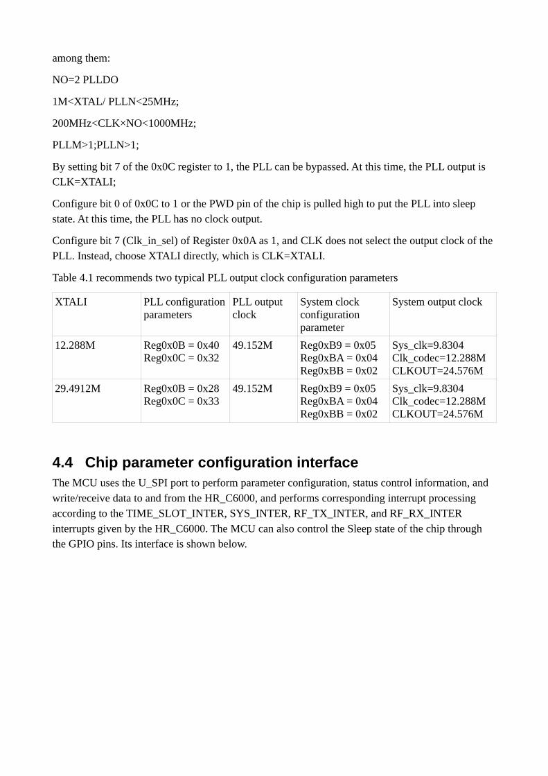
4.4 Chip parameter configuration interfaceThe MCU uses the U_SPI port to perform parameter configuration, status control information, and write/receive data to and from the HR_C6000, and performs corresponding interrupt processing according to the TIME_SLOT_INTER, SYS_INTER, RF_TX_INTER, and RF_RX_INTER interrupts given by the HR_C6000. The MCU can also control the Sleep state of the chip through the GPIO pins. Its interface is shown below.
OMISSIS
Figure 4.7 Interface between MCU and HR_C6000
The chip's U_SPI interface operates in Slave mode, and the interface timing is shown in the figure below.
OMISSIS
Figure 4.8 U_SPI Interface Read and Write Timing
SCLK supports up to 4MHz clock rate.
The MCU can control the Sleep state of the HR_C6000 through the GPIO pin. When the GPIO is pulled high, the chip is in the Sleep state, and all clocks in the HR_C6000 are turned off.

When the GPIO is pulled low again, the chip is in normal operation mode. In this case, the ByPass internal PLL needs to be used to provide the clock through the crystal XTALI direct HR_C6000. After waiting for more than 500μs. s, switch to the internal PLL to provide the HR_C6000 working clock.
As shown in the figure, XTALI is the crystal input clock signal, PWD is the sleep signal of HR_C6000, Sys_clk is the working clock of HR_C6000; PLL_Sys_clk is the clock obtained by dividing the frequency of HR_C6000 after the PLL output.
The MCU configuration PWD is high, and the PWD is stable after 100ns. At this time, the HR_C6000 internal clock is all cleared. After the PWD is pulled low again, the working clock needsto be switched to XTALI. After waiting for the PLL to stabilize the output of the divided PLL_Sys_clk, switch to the PLL. The divided output clock has a settling time greater than 500μs. s.
Figure 4.9 Schematic diagram of PWD control timing and working clock switching requirements
HR_C6000 provides 4 interrupt pins, the interrupt low pulse is valid, the pulse width is 3 system working clocks (Sys_clk, 9.8304MHz), SYS_INTER is to receive the indication interrupt of the system receiving and transmitting information, and the sending process and receiving process prompt the MCU status or control. TIME_SLOT_INTER is a 30ms time slot interrupt. This interrupt is generated cyclically after the HR_C6000 establishes a synchronization time slot. It is used to establish a TDMA time slot structure for the MCU. RF_TX_INTER and RF_RX_INTER are RF transceiver switching control interrupts. It is generated during the switching process to facilitate accurate and timely control of the RF channel by the MCU. RF_TX_INTER and RF_RX_INTER are alternately generated according to the period of 30ms. In order to facilitate the early start of the RF transmission control, register Reg0x12 can be set to control RF_TX_INTER and register Reg0xC0 to control RF_RX_INTER. The advance of 0ms can be configured with respect to the 30ms boundary.
OMISSIS
Figure 4.10 Schematic diagram of RF_TX_INTER and RF_RX_INTER generation
Table 4.2 RF_TX_INTER Interrupt Control Register Address Description
address function
0x12 Bit[5:0] configures the RF transceiver switching interrupt RF_TX_INTER relative to the 30ms boundary advance, in increments of 100μs. s. Bit[5:0] configures the RF transceiver switching interrupt RF_RX_INTER relative to the 30ms boundary advance, in increments of 100μs. s.
4.5 Use of CodecHR_C6000 built-in CodeC for Mic input and LINEOUT output, Mic gain control and LINEOUT
The volume control effectively reduces the user's peripheral devices. At the same time, the standard I2S interface is configured for the external CodeC, and the user can also select the appropriate Codec according to his own needs.
4.5.1 Built-in Codec
OMISSIS
4.5.2 Use external Codec
OMISSIS
Figure 4.13 Interface circuit with external Codec
When the HR_C6000 uses an external Codec, data is exchanged with Codec through the I2S interface. The interface timing is as follows.
OMISSIS
Figure 4.14 I2S Interface Timing
among them:
1. The LRCK clock frequency is determined by the Codec clock frequency and registers 0x32, 0x33. By default, the LRCK clock frequency is 8KHz.
LRCK clock frequency = Codec clock frequency / [2 * (parameter value + 1)], where the parameter value is derived from {register 0x32 value, register 0x33 value}.
2. The BCLK clock frequency is determined by the Codec clock frequency and registers 0x30, 0x31.
BCLK clock frequency = Codec clock frequency / [2 * (parameter value + 1)], where the parameter value is derived from {register 0x30 value, register 0x31 value}.
3. If the default external Codec (ALC5621) is used, LRCK is 8KHz and BCLK is 512KHz. At the same time, the chip CLKOUT pin needs to be connected to the chip MCLK pin, and CLKOUT outputs a 24.576MHz clock for the internal I2S operation of the chip. Connect theCLKOUT pin of the chip to the working clock input pin of Codec. When using the chip built-in Codec, the chip CLKOUT pin is not connected to the chip MCLK pin.
All pins of the external Codec can be reused as digital IO output, which can be used to control the high and low switching of the RF and the main control chip. The high and low switching time can be configured with reference to the delay of 30ms slot boundary or within 6ms in advance. The stepsize is 100us.
Table 4.4
Address Function
0xC7/C8 Control LRCK pin multiplexing, where Bit7 of C7 is multiplexed control enabled, Bit6 confirms high level with respect to 30ms slot boundary advance or delay, 0 is advanced, 1 is delayed; Bit5-0 is controlled early or delayed Quantity, the step size is 100us. Bit8 of C8 confirms that the low level is ahead or delayed relative to the 30mstime slot boundary, 0 is advanced, 1 is delayed; Bit5-0 is controlled early or delayed, and the step is 100us
0xC9/CA Control ADCDAT pin multiplexing. The definition is the same as LRCK multiplexing.
0xCB/CC Control MCLK pin multiplexing. The definition is the same as LRCK multiplexing.
0xCD/CE Control BCLK pin multiplexing. The definition is the same as LRCK multiplexing.
0xCF/D0 Control DACDAT pin multiplexing. The definition is the same as LRCK multiplexing.
As shown in the figure below, the control of the LRCK pin is taken as an example to illustrate the control diagram of the high and low levels. The other pin control methods are the same as this.
OMISSIS
Figure 4.15 LRCK pin multiplexing for general IO control interface timing
4.6 VocoderHR_C6000 can seamlessly interface with vocoder chips such as AMBE3000 and AMBE1000 with McBSP and CHS serial interface, and provide standard SPI and IS interfaces, and with Macro Rui HR_V3000 vocoder, Tsinghua SELP vocoder, 712 factory AVDS vocoder. Splicing docking, support for encrypted voice, data interface, and provide interface for digital voice recording, playback and prompt tone input.
4.6.1 Interface definition with Hongrui HR_V3000 vocoder
HR_V3000 and HR_C6000 transmit the compression-encoded digital voice stream or the digital voice stream to be decoded through V_SPI, and transmit PCM data through the I 2 S interface and the vocoder. The 2 IS interface of HR_C6000 works in the master mode; the MCU passes the UART interface. Transfer the voice encryption/decryption key or voice frame synchronization information with HR_V3000. The interface timing of the V_SPI port is shown in the figure below.

Figure 4.16 Using the V_SPI Interface to Read (Write) Timing
The SCLK supports up to 4MHz clock rate.
The frame format of V_SPI is shown below. What needs to be explained is:
The V_SPI interface can only perform one operation at a time, read or write.
When performing a read operation, Cmd=0x83, Addr=0x00, and read 27 individual Data(byte).
When writing, Cmd=0x03, Addr=0x00, and write 27 individual Data(byte).
OMISSIS
Cmd Addr Data0 Data1… Datan
Figure 4.17 V_SPI frame format
To communicate with the Hongrui HR_V3000 vocoder via the V_SPI interface HR_C6000, simply configure the HR_C6000 register reg0x06 to 0x24. The connection diagram of HR_V3000 and HR_C6000 and MCU is shown in the figure.
OMISSIS
Figure 4.18 HR_V3000 vocoder and HR_C6000 connection block diagram
OMISSIS
Figure 4.19 shows the interface timing of I2S.
I2S operates in master mode and needs to configure the I2S_CK_M clock frequency via Register 0x2F, calculated as codec operating frequency / (2* (Register 0x2F value + 1)). The I2S_FS_M clock frequency is configured by Register 0x32, 0x33 (the configured I2S_FS_M clock frequency must be 8KHz), calculated as codec operating frequency / (2 * ({Register 0x32 value, 0x33 value} +1)). At the same time, the I2S_CK_M frequency is >34* I2S_FS_M frequency, and the codec clock frequency is >=6*I2S_CK_M frequency.
When I2S is operating in Master mode, the I2S_CK_M, I2S_FS_M signals can be turned off via Register 0x36[6]. When 0x36[6]=0, these two signals are turned on, otherwise the two signals are turned off.
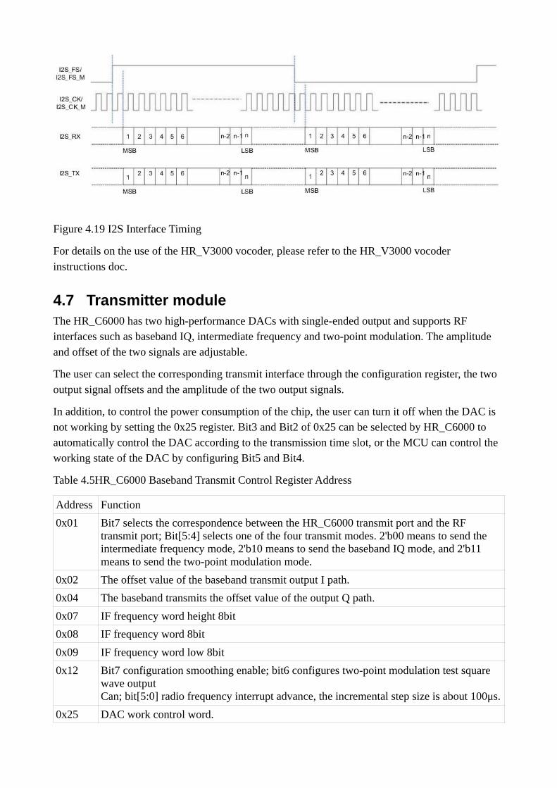
Figure 4.19 I2S Interface Timing
For details on the use of the HR_V3000 vocoder, please refer to the HR_V3000 vocoder instructions doc.
4.7 Transmitter moduleThe HR_C6000 has two high-performance DACs with single-ended output and supports RF interfaces such as baseband IQ, intermediate frequency and two-point modulation. The amplitude and offset of the two signals are adjustable.
The user can select the corresponding transmit interface through the configuration register, the two output signal offsets and the amplitude of the two output signals.
In addition, to control the power consumption of the chip, the user can turn it off when the DAC is not working by setting the 0x25 register. Bit3 and Bit2 of 0x25 can be selected by HR_C6000 to automatically control the DAC according to the transmission time slot, or the MCU can control the working state of the DAC by configuring Bit5 and Bit4.
Table 4.5HR_C6000 Baseband Transmit Control Register Address
Address Function
0x01 Bit7 selects the correspondence between the HR_C6000 transmit port and the RF transmit port; Bit[5:4] selects one of the four transmit modes. 2'b00 means to send the intermediate frequency mode, 2'b10 means to send the baseband IQ mode, and 2'b11 means to send the two-point modulation mode.
0x02 The offset value of the baseband transmit output I path.
0x04 The baseband transmits the offset value of the output Q path.
0x07 IF frequency word height 8bit
0x08 IF frequency word 8bit
0x09 IF frequency word low 8bit
0x12 Bit7 configuration smoothing enable; bit6 configures two-point modulation test square wave outputCan; bit[5:0] radio frequency interrupt advance, the incremental step size is about 100μs. s.
0x25 DAC work control word.
0x2E Send the advance configuration value. Because the RF channel delay is different, to ensure that the airborne DMR signal is strictly corresponding to the slot boundary transmission, configuring this register can offset the delay amount, and the step is 100μs. s.The internal channel has a fixed delay of 400μs. s, so this register should be configured as 0x04 when there is no delay on the RF side.
0x45 Adjust the amplitude of the two-point modulation MOD2 (DAC_IVOUT)
0x46 Adjust the amplitude of the two-point modulation MOD1 (DAC_QVOUT)
0x47 Define two-point modulation offset adjustment value, a total of 10bit, where the high 2bit is defined in the lower 2bit of reg0x48.
0x48 Bit[1:0] defines two-point modulation offset adjustment value, a total of 10bit, of which the lower 8bit is defined in reg0x47
4.7.1 Baseband IQ modulation
OMISSIS
4.7.2 Two-point modulation
OMISSIS
4.7.3 IF IQ modulation
OMISSIS
4.7.4 IF modulation
OMISSIS
4.8 Receiving moduleOMISSIS
4.8.1 Baseband IQ
OMISSIS
4.8.2 IF mode
OMISSIS
5 Hierarchical function descriptionHR_C6000 adopts a flexible layered design model to flexibly open different levels for users to meetdifferent user needs.
The layered design uses a three-tier architecture as shown.
Control and data services Voice service
• Call control layer

• Data link layer
• Physical layer
OMISSIS
Figure 5.1 HR_C6000 three-tier open architecture
The one-layer mode mainly solves the channel filtering of the baseband or low-IF signal and the modulation and demodulation process of the signal, as defined in the green dotted box in the above figure. The user needs to solve the channel codec and the processing of all communication protocol stacks by using one layer mode, which has the greatest development flexibility and development workload.
The second layer mode is mainly based on the opening of one layer of all content, completes the coding and decoding of the channel, and interleaves, deinterleaves and checksums, etc., as defined in the gray dashed box in the above figure. The user only needs to solve the processing flow of the communication protocol stack, and has greater development flexibility and moderate development workload.
The three-layer mode refers to all the application functions defined by the HR_C6000 according to the DMR protocol, and completes the modulation and demodulation, codec, and protocol stack design of all standardized application functions, all the functions defined in the blue dotted box in the above figure.
Users use these application functions, and only need to configure the corresponding function registers, so that all DMR protocol customized voice and data services can be quickly and conveniently used.
The HR_C6000 is mainly developed based on the Layer 2 mode. The user does not need to pay attention to the codec interleaving of the channel and the underlying modulation and demodulation process.
5.1 Interrupt use instructions
5.1.1 Interrupt use description
The corresponding interrupt of the three-layer function is sys_inter. The interrupt consists of two sub-interrupts. After receiving the interrupt, the MCU reads the interrupt status register 0x82. The corresponding interrupt can be masked by register 0x81, and the corresponding interrupt is cleared by register 0x83. A list of bit interrupt signals that yields 8 types of interrupts, including:
Bit7: In DMR mode: indicates that the transmission request rejects the interrupt without a sub-statusregister.
In DMR mode, it indicates that this transmission request is rejected because the channel is busy;
Bit6: In DMR mode: indicates the start of transmission; in MSK mode: indicates that the ping-pong buffer is half-full interrupted. In DMR mode, the sub-status register 0x84 is transmitted at the beginning, and the corresponding interrupt can be masked by 0x85. The sub-status registers indicateseven interrupts that initiate the transmission, including:
Bit7: Voice transmission starts
Bit6: OACSU requests to send interrupts, including first-time send and resend requests.
Bit5: End-to-end voice enhanced encryption interrupt, including EMB72bits update interruptand voice 216bits key update interrupt, which are distinguished by Bit5~Bit4 of Register 0x88, where 01 indicates EMB72bits update interrupt and 10 indicates voice 216bits key update interrupt.
Bit4: The Vocoder configuration returns an interrupt (this interrupt is sent by the HR_C6000 to the MCU when the MCU manually configures the AMBE3000). This interrupt is only valid when using the external AMBE3000 vocoder.
Bit3: Data transmission starts
Bit2: Data partial retransmission
Bit1: Data retransmission
Bit0: The vocoder is initialized to an interrupt. This interrupt is only valid when using an external AMBE3000 or AMBE1000 vocoder.
In MSK mode, there is no sub-interrupt status.
Bit5: In DMR mode: indicates the end of transmission; in MSK mode: indicates the end of transmission.
In DMR mode, there is a sub-status register 0x86 at the end of the transmission, and the corresponding interrupt can be masked by 0x87. The sub-status register indicates six interrupts that generate the end of the transmission, including:
Bit7: indicates that the service transmission is completely terminated, including voice and data. The MCU distinguishes whether the voice or data is sent this time. Confirming that the data service is received is the response packet that receives the correct feedback.
Bit6: Indicates that a Fragment length confirmation packet is sent in the sliding window dataservice without immediate feedback.
Bit5: Voice OACSU wait timeout
Bit4: The Layer 2 mode handles the interrupt. The MCU sends the configuration informationto the last processing timing of the chip to control the interrupt. If after the interrupt, the MCU has not written all the information to be sent in the next frame to the chip, the next time slot cannot be Configured to send time slots. This interrupt is only valid when the chip is operating in Layer 2 mode.
Bit3: indicates that a Fragment that needs to be fed back confirms the completion of the datapacket transmission. The interrupt is mainly applied to the acknowledgment message after all the data packets have been sent or the data packet that needs to be fed back in the sliding window data service is sent to the MCU to start waiting for the timing of the Response packet. Device.
Bit2 : ShortLC Receive Interrupt
Bit1: BS activation timeout interrupt
In MSK mode, there is no substate interrupt.
Bit4: In DMR mode: indicates the access interruption; in MSK mode: indicates that the response response is interrupted. In DMR mode, the access interrupt has no sub-status register. After receiving the interrupt, it indicates that the access voice communication mode is post-access. the way.
In MSK mode, this interrupt has no substatus registers.
Bit3: In DMR mode: indicates that the control frame parsing completion interrupt; in MSK mode: indicates the receive interrupt.
In DMR mode, this interrupt has no sub-status register, but the error and receive type of its receiveddata is given by the 0x51 register. The DLLRecvDataType, DLLRecvCRC are used to indicate the received data type and the error status, and the MCU accordingly performs the corresponding status.Display, you can also block the corresponding interrupt.
In MSK mode, this interrupt has no substate interrupts.
The FMB frame's EMB information parsing completion prompt is also the completion of the interrupt, which is distinguished by judging the 0x51 register SyncClass=0.
Bit2: In DMR mode: indicates service data reception interrupt; in FM mode: indicates FM function detection interrupt.
In DMR mode, this interrupt has sub-status register 0x90, which has three types:
1. 0x80 indicates that the entire information is received and verified. After the service data is verified, the MCU extracts the data after the address 0x30 in the RX terminal 1.2KRAM through the SPI port. The length of the data is defined by the corresponding field of the received frame header.
2. 0x00 indicates the entire information reception check error;
3. 0x40 indicates that a non-confirmed SMS abnormal interrupt is generated;
In FM mode, the interrupt has sub-status register 0x90, and the sub-status register has 1 type:
1. 0x10 indicates that the FM function detection interrupt is matched. When the FM interrupt isdetected in the FM mode, the corresponding analog sound output is turned on.
Bit1: In DMR mode: indicates that the voice is abnormally exited;
In DMR mode, the cause of the abnormality in DMR mode is the unexpected abnormal voice interrupt generated inside the state machine. The corresponding voice exception type is obtained through Bit2~Bit0 of register address 0x98.
Bit0: physical layer separate work reception interrupt
The physical layer works independently to receive interrupts without a sub-status register. The interrupt is generated in the physical layer single working mode. After receiving the data, the interrupt is generated, and the MCU is notified to read the corresponding register to obtain the
received data. This interrupt is typically tested in bit error rate or other performance in physical layer mode.
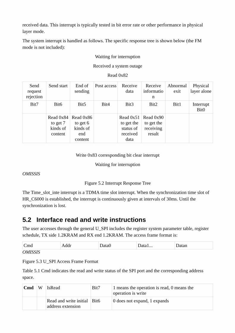
The system interrupt is handled as follows. The specific response tree is shown below (the FM mode is not included):
Waiting for interruption
Received a system outage
Read 0x82
Sendrequest
rejection
Send start End ofsending
Post access Receivedata
Receiveinformatio
n
Abnormalexit
Physicallayer alone
Bit7 Bit6 Bit5 Bit4 Bit3 Bit2 Bit1 InterruptBit0
Read 0x84to get 7kinds ofcontent
Read 0x86to get 6kinds of
endcontent
Read 0x51to get thestatus ofreceived
data
Read 0x90to get thereceiving
result
Write 0x83 corresponding bit clear interrupt
Waiting for interruption
OMISSIS
Figure 5.2 Interrupt Response Tree
The Time_slot_inte interrupt is a TDMA time slot interrupt. When the synchronization time slot of HR_C6000 is established, the interrupt is continuously given at intervals of 30ms. Until the synchronization is lost.
5.2 Interface read and write instructionsThe user accesses through the general U_SPI includes the register system parameter table, register schedule, TX side 1.2KRAM and RX end 1.2KRAM. The access frame format is:
Cmd Addr Data0 Data1... DatanOMISSIS
Figure 5.3 U_SPI Access Frame Format
Table 5.1 Cmd indicates the read and write status of the SPI port and the corresponding address space.
Cmd W IsRead Bit7 1 means the operation is read, 0 means the operation is write
Read and write initial address extension
Bit6 0 does not expand, 1 expands
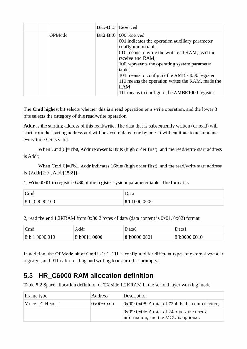
Bit5-Bit3 Reserved
OPMode Bit2-Bit0 000 reserved001 indicates the operation auxiliary parameter configuration table.010 means to write the write end RAM, read the receive end RAM,100 represents the operating system parameter table,101 means to configure the AMBE3000 register110 means the operation writes the RAM, reads the RAM,111 means to configure the AMBE1000 register
The Cmd highest bit selects whether this is a read operation or a write operation, and the lower 3 bits selects the category of this read/write operation.
Addr is the starting address of this read/write. The data that is subsequently written (or read) will start from the starting address and will be accumulated one by one. It will continue to accumulate every time CS is valid.
When Cmd[6]=1'b0, Addr represents 8bits (high order first), and the read/write start address is Addr;
When Cmd[6]=1'b1, Addr indicates 16bits (high order first), and the read/write start address is {Addr[2:0], Addr[15:8]}.
1. Write 0x01 to register 0x80 of the register system parameter table. The format is:
Cmd Data
8’b 0 0000 100 8’b1000 0000
2, read the end 1.2KRAM from 0x30 2 bytes of data (data content is 0x01, 0x02) format:
Cmd Addr Data0 Data1
8’b 1 0000 010 8’b0011 0000 8’b0000 0001 8’b0000 0010
In addition, the OPMode bit of Cmd is 101, 111 is configured for different types of external vocoderregisters, and 011 is for reading and writing tones or other prompts.
5.3 HR_C6000 RAM allocation definitionTable 5.2 Space allocation definition of TX side 1.2KRAM in the second layer working mode
Frame type Address Description
Voice LC Header 0x00~0x0b 0x00~0x08: A total of 72bit is the control letter;
0x09~0x0b: A total of 24 bits is the check information, and the MCU is optional.

Voice PI Header 0x00~0x0b 0x00~0x09: A total of 80 bits is the control information;
0x0a~0x0b: A total of 16 bits is the check information, and the MCU is optional.
Voice EMB 0x00~0x09 0x00~0x08: A total of 72bit is the control letter;
0x09: bit7-bit3 A total of 5 bits is the check information, and the MCU is optional.
The information here is prepared at the same time as the speech frame A is to be sent.
Voice A 0x30~0x4a A total of 216 bits is voice frame information.
Voice B 0x30~0x4a A total of 216 bits is voice frame information.
Voice C 0x30~0x4a A total of 216 bits is voice frame information.
Voice D 0x30~0x4a A total of 216 bits is voice frame information.
Voice E 0x30~0x4a A total of 216 bits is voice frame information.
Voice F 0x30~0x4a A total of 216 bits is voice frame information.
RC Frame 0x00~0x01 0x00, bit7-bit5 of 0x01, total 11bit information
Voice Terminator 0x00~0x0b 0x00~0x08: A total of 72bit is the control letter;
0x09~0x0b: A total of 24 bits is the check information, and the MCU is optional.
CSBK 0x00~0x0b 0x00~0x09: A total of 80 bits is the control information;
0x0a~0x0b: A total of 16 bits is the check information, and the MCU is optional.
MBC Header 0x00~0x0b 0x00~0x09: A total of 80 bits is the control information;
0x0a~0x0b: A total of 16 bits is the check information, and the MCU is optional.
MBC Intermedia 0x00~0x0b 0x00~0x0b: A total of 96 bits is the control information;
MBC Last 0x00~0x0b 0x00~0x0b: A total of 96 bits is the control information;
DataHeader 0x00~0x0b 0x00~0x09: A total of 80 bits is the control information;
0x0a~0x0b: A total of 16 bits is the check information, and the MCU is optional.
DataRate1_2 0x00~0x0b 0x00~0x0b: A total of 96 bits is data information;
DataRate3_4 0x00~0x11 0x00~0x11: A total of 144 bits is data information;
DataRate1 0x00~0x17 0x00~0x17: A total of 192 bits is data information;
Idle 0x18~0x23 0x18~0x23: A total of 96 bits is the control information;
Short LC 0x24~0x28 0x24~0x26, bit7-bit4 of 0x27: total 28bit control information;
0x28 : A total of 8bit check information.
Voice F frame EMB 0x29~0x2C Voice F frame fill information
Or 0x29 stores the superframe number (KeyID), 0x2A high 3bit stores the encryption serial number (ALOG ID)
Data control frame EMB RC 0x4b~0x50 Data control frame embedded 48bit RC information or 0x4b, 0x4c
High 11bit RC encoder input
C_RC frame (PDT) 0x00~0x0a 0x00, bit7-bit5 of 0x01: total 11bit RC information;
0x02~0x08: Total 56 bit control information;
0x09~0x0a: Total 16 bit check information;
196 message/information 0x30~0x48 196bit control information
Test send 0x00~0x48 Send mode test to store data address
FM data address 1 0x030~0x22f A total of 512 bytes of data information. You can send voice data for externally written FM or internally send voice data from Codec
FM data address 2 0x230~0x42f A total of 512 bytes of data information. You can send voice data for externally written FM or internally send voice data from Codec
Encryption key stream data storage
0x495~0x4af A total of 216bit, 27 bytes
Table 5.3 Space allocation definition of RX terminal 1.2KRAM in the two-layer working mode
OMISSIS
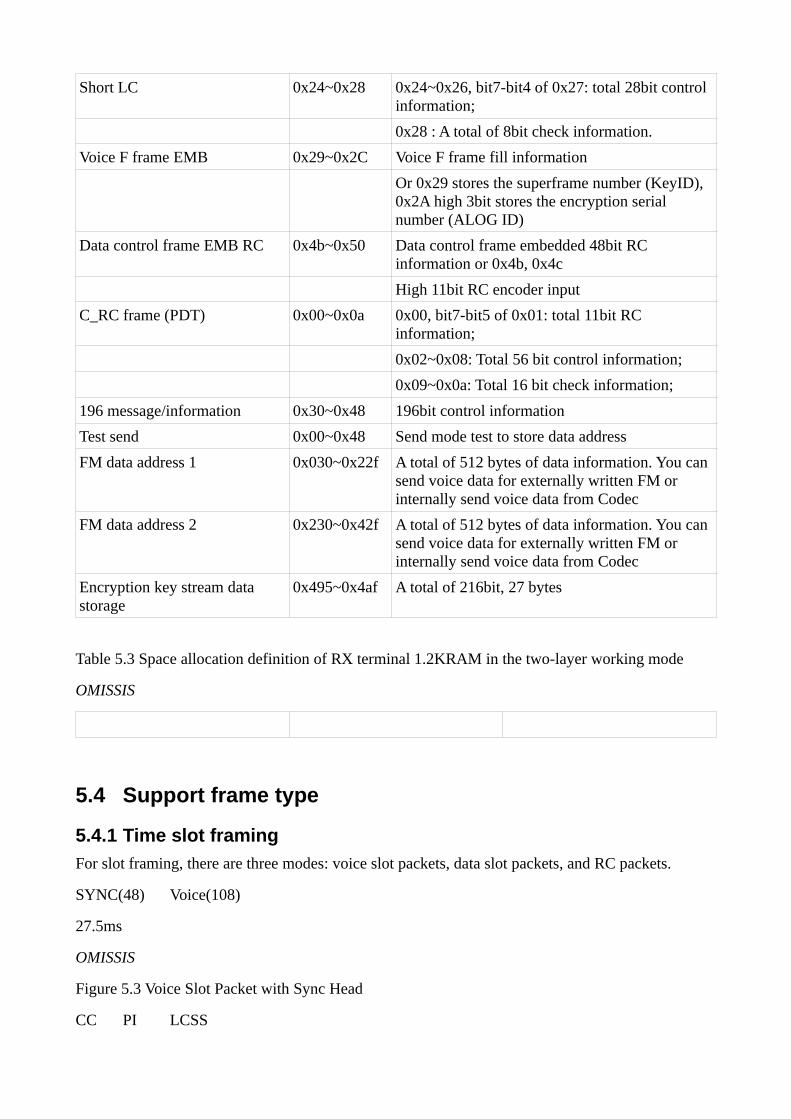
5.4 Support frame type
5.4.1 Time slot framing
For slot framing, there are three modes: voice slot packets, data slot packets, and RC packets.
SYNC(48) Voice(108)
27.5ms
OMISSIS
Figure 5.3 Voice Slot Packet with Sync Head
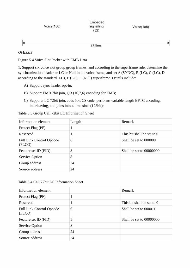
CC PI LCSS
OMISSIS
Figure 5.4 Voice Slot Packet with EMB Data
1. Support six voice slot group group frames, and according to the superframe rule, determine the synchronization header or LC or Null in the voice frame, and set A (SYNC), B (LC), C (LC), D according to the standard. LC), E (LC), F (Null) superframe. Details include:
A) Support sync header opt-in;
B) Support EMB 7bit join, QR (16,7,6) encoding for EMB;
C) Supports LC 72bit join, adds 5bit CS code, performs variable length BPTC encoding, interleaving, and joins into 4 time slots (128bit);
Table 5.3 Group Call 72bit LC Information Sheet
Information element Length Remark
Protect Flag (PF) 1
Reserved 1 This bit shall be set to 0
Full Link Control Opcode (FLCO)
6 Shall be set to 000000
Feature set ID (FID) 8 Shall be set to 00000000
Service Option 8
Group address 24
Source address 24
Table 5.4 Call 72bit LC Information Sheet
Information element Remark
Protect Flag (PF) 1
Reserved 1 This bit shall be set to 0
Full Link Control Opcode (FLCO)
6 Shall be set to 000011
Feature set ID (FID) 8 Shall be set to 00000000
Service Option 8
Group address 24
Source address 24
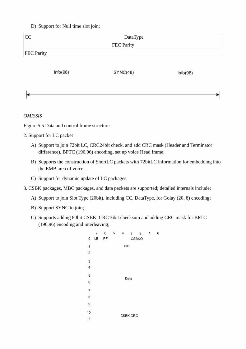
D) Support for Null time slot join;
CC DataType
FEC Parity
FEC Parity
OMISSIS
Figure 5.5 Data and control frame structure
2. Support for LC packet
A) Support to join 72bit LC, CRC24bit check, and add CRC mask (Header and Terminator difference), BPTC (196,96) encoding, set up voice Head frame;
B) Supports the construction of ShortLC packets with 72bitLC information for embedding into the EMB area of voice;
C) Support for dynamic update of LC packages;
3. CSBK packages, MBC packages, and data packets are supported; detailed internals include:
A) Support to join Slot Type (20bit), including CC, DataType, for Golay (20, 8) encoding;
B) Support SYNC to join;
C) Supports adding 80bit CSBK, CRC16bit checksum and adding CRC mask for BPTC (196,96) encoding and interleaving;
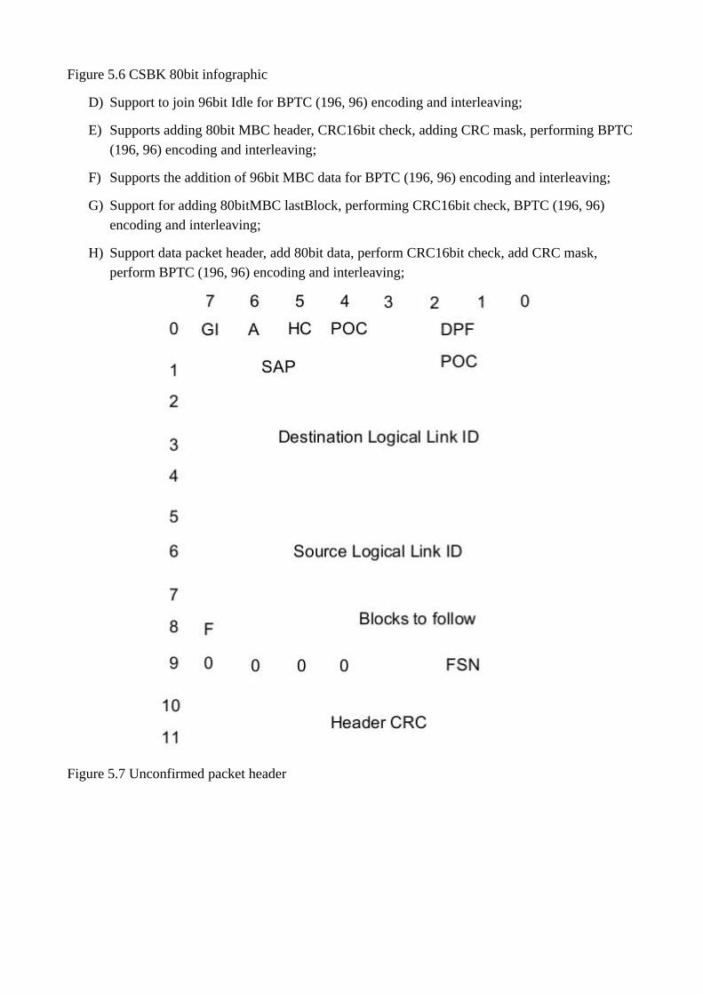
Figure 5.6 CSBK 80bit infographic
D) Support to join 96bit Idle for BPTC (196, 96) encoding and interleaving;
E) Supports adding 80bit MBC header, CRC16bit check, adding CRC mask, performing BPTC (196, 96) encoding and interleaving;
F) Supports the addition of 96bit MBC data for BPTC (196, 96) encoding and interleaving;
G) Support for adding 80bitMBC lastBlock, performing CRC16bit check, BPTC (196, 96) encoding and interleaving;
H) Support data packet header, add 80bit data, perform CRC16bit check, add CRC mask, perform BPTC (196, 96) encoding and interleaving;
Figure 5.7 Unconfirmed packet header
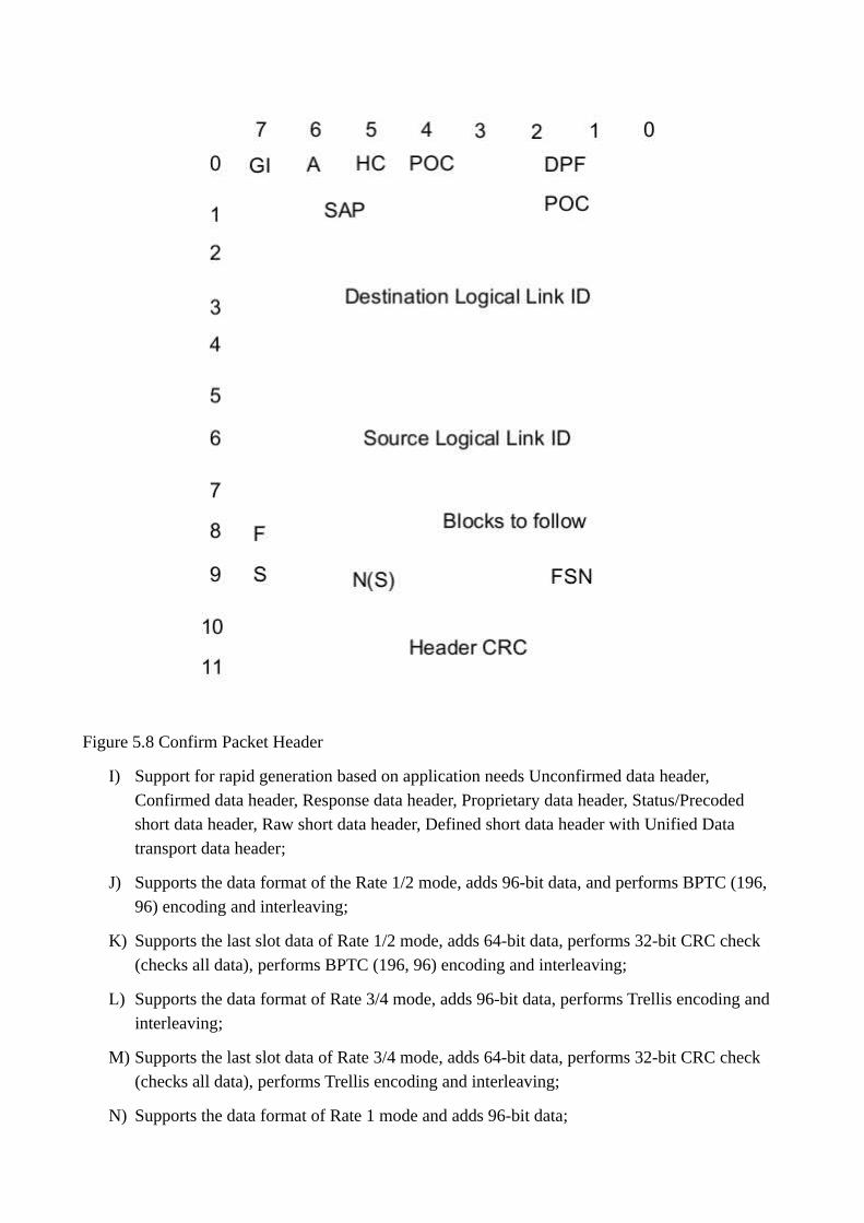
Figure 5.8 Confirm Packet Header
I) Support for rapid generation based on application needs Unconfirmed data header, Confirmed data header, Response data header, Proprietary data header, Status/Precoded short data header, Raw short data header, Defined short data header with Unified Data transport data header;
J) Supports the data format of the Rate 1/2 mode, adds 96-bit data, and performs BPTC (196, 96) encoding and interleaving;
K) Supports the last slot data of Rate 1/2 mode, adds 64-bit data, performs 32-bit CRC check (checks all data), performs BPTC (196, 96) encoding and interleaving;
L) Supports the data format of Rate 3/4 mode, adds 96-bit data, performs Trellis encoding and interleaving;
M) Supports the last slot data of Rate 3/4 mode, adds 64-bit data, performs 32-bit CRC check (checks all data), performs Trellis encoding and interleaving;
N) Supports the data format of Rate 1 mode and adds 96-bit data;

O) Supports the last slot data of Rate 1 mode, adds 64-bit data, and performs 32-bit CRC check (checksum contains all data);
P) Supports three types of confirmed data transmission, joins 7bit SN, performs 9-bit CRC check, adds masks (different rates, different masks), encodes and interleaves at different rates, and adds 32-bit CRC to the data;
Q) Support feedback packet data time slot, add 1-2 data feedback packets, perform overall 32-bit CRC check, perform BPTC (196, 96) encoding and interleaving;
R) Support UDT's last block, perform 16-bit CRC check on data, perform BPTC (196, 96) encoding and interleaving;
CC PI LCSS
RC Info + FEC Parity
RC Info + FEC Parity
SYNC
SYNC
SYNC
SYNC
SYNC
SYNC
RC Info + FEC Parity
RC Info + FEC Parity
EMB Parity
SYNC(48)
10ms
30ms
OMISSIS
Figure 5.9 Independent RC frame structure
4. Supports RC signals for time slots RC and EMB;
A) Support for adding 7bitEMB for QR (16, 7, 6) encoding;
B) Support for adding 11bit RC signals, performing variable length BPTC, interleaving 32bit, and adding to RC unit;
5. Receiving the content type of the frame determined according to SYNC, determining the type of the received frame according to Slot Type, FLCO, CSBKO, LB, DPF, and then performing deinterleaving, decoding, and verifying corresponding to the transmission according to the received frame type.
5.4.2 Framing mode
Continuous mode:
OMISSIS
Slot mode:
1) Supports voice superframe framing, which can be set to LC Header, PI Header or PI Header mode only, and automatically constitutes a superframe and joins LC Terminator;
2) Support 4.8kbps framing for various data types, adding data LC Header, data and LC Terminator;
5.4.3 Frame definition and use
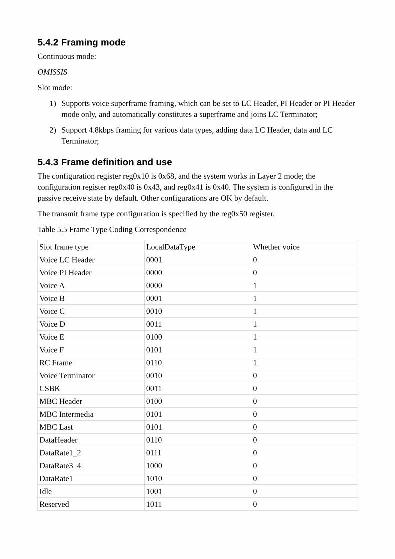
The configuration register reg0x10 is 0x68, and the system works in Layer 2 mode; the configuration register reg0x40 is 0x43, and reg0x41 is 0x40. The system is configured in the passive receive state by default. Other configurations are OK by default.
The transmit frame type configuration is specified by the reg0x50 register.
Table 5.5 Frame Type Coding Correspondence
Slot frame type LocalDataType Whether voice
Voice LC Header 0001 0
Voice PI Header 0000 0
Voice A 0000 1
Voice B 0001 1
Voice C 0010 1
Voice D 0011 1
Voice E 0100 1
Voice F 0101 1
RC Frame 0110 1
Voice Terminator 0010 0
CSBK 0011 0
MBC Header 0100 0
MBC Intermedia 0101 0
MBC Last 0101 0
DataHeader 0110 0
DataRate1_2 0111 0
DataRate3_4 1000 0
DataRate1 1010 0
Idle 1001 0
Reserved 1011 0
1100 0
1011 0
1110 0
1111 0
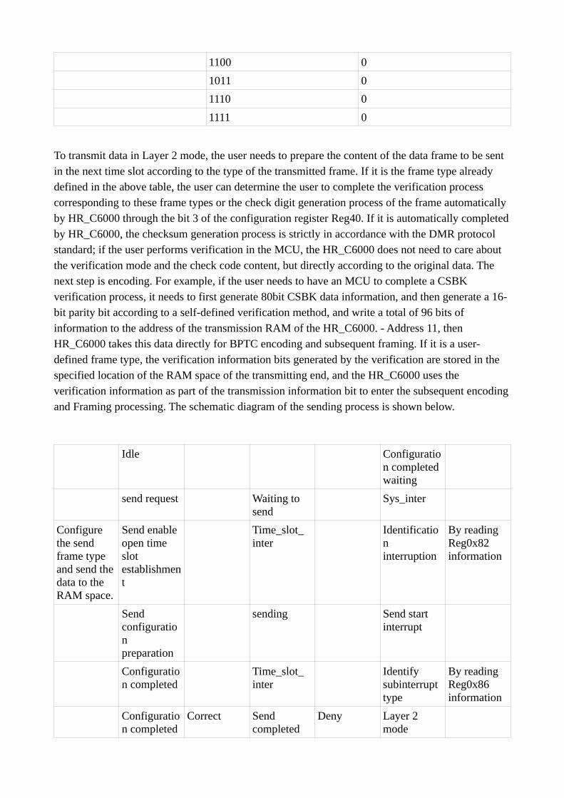
To transmit data in Layer 2 mode, the user needs to prepare the content of the data frame to be sent in the next time slot according to the type of the transmitted frame. If it is the frame type already defined in the above table, the user can determine the user to complete the verification process corresponding to these frame types or the check digit generation process of the frame automatically by HR_C6000 through the bit 3 of the configuration register Reg40. If it is automatically completedby HR_C6000, the checksum generation process is strictly in accordance with the DMR protocol standard; if the user performs verification in the MCU, the HR_C6000 does not need to care about the verification mode and the check code content, but directly according to the original data. The next step is encoding. For example, if the user needs to have an MCU to complete a CSBK verification process, it needs to first generate 80bit CSBK data information, and then generate a 16-bit parity bit according to a self-defined verification method, and write a total of 96 bits of information to the address of the transmission RAM of the HR_C6000. - Address 11, then HR_C6000 takes this data directly for BPTC encoding and subsequent framing. If it is a user-defined frame type, the verification information bits generated by the verification are stored in the specified location of the RAM space of the transmitting end, and the HR_C6000 uses the verification information as part of the transmission information bit to enter the subsequent encodingand Framing processing. The schematic diagram of the sending process is shown below.
Idle Configuration completed waiting
send request Waiting to send
Sys_inter
Configure the send frame type and send the data to the RAM space.
Send enable open time slot establishment
Time_slot_inter
Identification interruption
By reading Reg0x82 information
Send configuration preparation
sending Send start interrupt
Configuration completed
Time_slot_inter
Identify subinterrupt type
By reading Reg0x86 information
Configuration completed
Correct Send completed
Deny Layer 2 mode
waiting transmissionpreparation interrupt
Idle Send configuration preparation
Enable the next time slot transmissionenable
Figure 5.10 Flow chart of the Layer 2 sending process
5.4.4 Working mode description
Working in Layer 2 mode, the synchronization time axis of the 30ms time slot required in the wholemachine is provided by HR_C6000, while the HR_C6000 provides 30ms time axis. There are two modes, one is generated by HR_C6000 own clock, which provides 30ms stably. Interrupt, called active mode, the other is that the 30ms interrupt provided by HR_C6000 will continuously adjust its30ms (approximate) interrupt output according to the signal received by HR_C6000 (including the sync head signal), which is called passive mode.
Active mode: CPU setting HR_C6000 Active mode (Register reg0x40 Bit5 is configured to 1, 1 of Bit6 and Bit7 must be 1), establish a time slot, and provide 30ms interrupt to the MCU.
Passive mode: CPU setting HR_C6000 register reg0x40 Bit5 is configured as 0 (where Bit6 and Bit7 must have one). HR_C6000 enters the receiving state. The system starts to establish synchronization according to the synchronization information of the received signal, and continues to receive synchronization information according to the received information. To adjust the synchronization timeline to provide a 30ms (approximate) interrupt to the MCU.
After the complete time axis is established, the chip has the conditions for sending and receiving. On this basis, the chip will provide the CPU time slot interrupt Time_slot_inter, which is used to inform the CPU of the middle position of the time slot of the entire time axis. The CPU plans the corresponding according to the time axis. Receive, send, and perform correct control and data transmission.
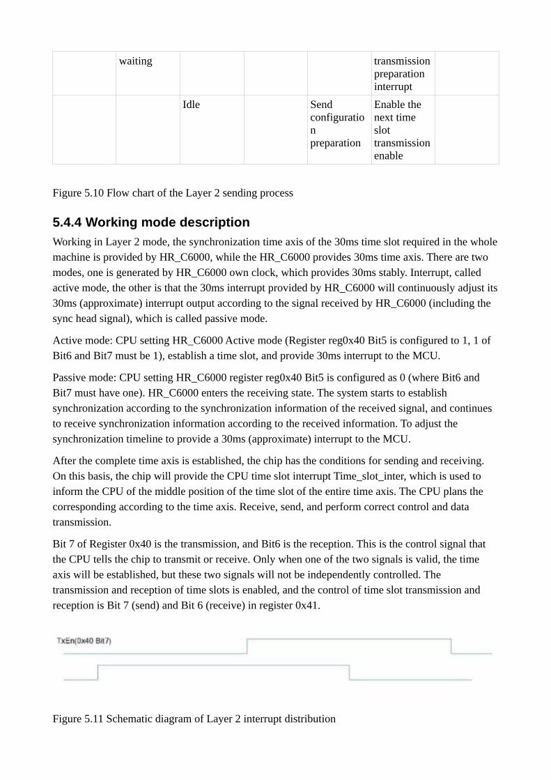
Bit 7 of Register 0x40 is the transmission, and Bit6 is the reception. This is the control signal that the CPU tells the chip to transmit or receive. Only when one of the two signals is valid, the time axis will be established, but these two signals will not be independently controlled. The transmission and reception of time slots is enabled, and the control of time slot transmission and reception is Bit 7 (send) and Bit 6 (receive) in register 0x41.
Figure 5.11 Schematic diagram of Layer 2 interrupt distribution
In Layer 2 mode, once the time axis is established (whether passive or active), the chip will continue to give the TIME_SLOT_INTER and Rdy_lst_inter shown in the figure above for 30ms. Rdy_lst_inter is not a separate interrupt pin. The terminal multiplexes an interrupt pin output with Sys_inter. The multiplexing mode is the same as the three-layer interrupt usage description in 5.1.1.
The t1 time is the start time of the code sending framing frame, t2 is the software preparation data and the configuration transceiver control command time, and t3 is the time from the end of the time slot to the Sys_inter interrupt to the CPU.
The chip is in position 1 or position 2, giving TIME_SLOT_INTER or Rdy_lst_Inter. The CPU can set the time slot 2 to be transmitted or received according to one of the two interrupts (0x41, Bit7, Bit6).
If time slot 1 is received, then at position 4 the CPU can read the data received in that time slot and provide a decision basis for the next action of the CPU.
Assuming that time slot 1 is received, and time slot 2 is set to transmit after the position 1 (TIME_SLOT_INTER interrupt) and before position 2 (Rdy_lst_inter interrupt), the chip will give RF_TX_INTER for the CPU to set the RF channel correlation. parameter.
Assuming that time slot 1 is a transmission, and time slot 2 is set to receive after the position 1 (TIME_SLOT_INTER interrupt) and before position 2 (Rdy_lst_inter interrupt), the chip will give RF_RX_INTER for the CPU to set the RF channel correlation. parameter.
According to the active-passive mode established by the time axis, the transmission and reception mode control of the time slot of the whole machine is combined into a working mode:
1) Active sending
Active sending means that the system is currently in an out-of-synchronization state, initiates a call, and generates synchronization information locally. This situation is mainly applied to the HR_C6000 initiative to initiate single and duplex transmission.
MCU setting send register 0x40 turn on active send 0xA3;
The establishment of this flag bit will cause the chip to generate active transmission synchronizationinformation, and send a 30ms interval interrupt to the MCU through TIME_SLOT_INTER;
After receiving the 30ms interrupt, the MCU reads the 0x42 status bit7-5 and judges the current time slot transmission and reception:
001 indicates that the current time slot is a working time slot, but the transceiver is fully closed;
101 indicates that the current time slot is a working time slot, and the sending is enabled;
011 indicates that the current time slot is a working time slot, and reception is enabled.
xx0 indicates that the current time slot is a non-working time slot, and the transceiver does not need to be opened;
The MCU obtains the time slot transmission and reception status of the HR_C6000 to determine theoperation requirement of the next time slot according to the protocol.
After the 30ms synchronization time slot is established, if the next time slot needs to be sent, write framing is required in t2 (including 196bit rate 1 data stream, 144bit rate 3/4 data stream, 96bit rate 1/2 data stream, 96bit Custom control information frame, 80bit data frame header or CSBK data frame, 72bit voice frame header, end of frame data, data format and content requirements are designed according to DMR protocol standard. When receiving Rdy_lst_inter interrupt, set the value of register 0x41. To determine whether the next time slot is sent 0x80 (send), 0x00 (not sent); if the Rdy_lst_inter interrupt is masked, the 0x41 register can be directly configured in the 30ms interrupt (TIMER_SLOT_INTER, position 1 in the figure), that is, the configuration is sent and not sent first. For data writing, this requires the user to ensure that all data preparations that require framing are completed within t2.
The chip reads the Bit7 flag of 0x40 at the beginning of the t1 time. If it is 1, the data in the data buffer will be mapped and sent in t1 time.
The CPU can configure the relevant RF channel for transmission according to the RF_Tx_Inter interrupt.
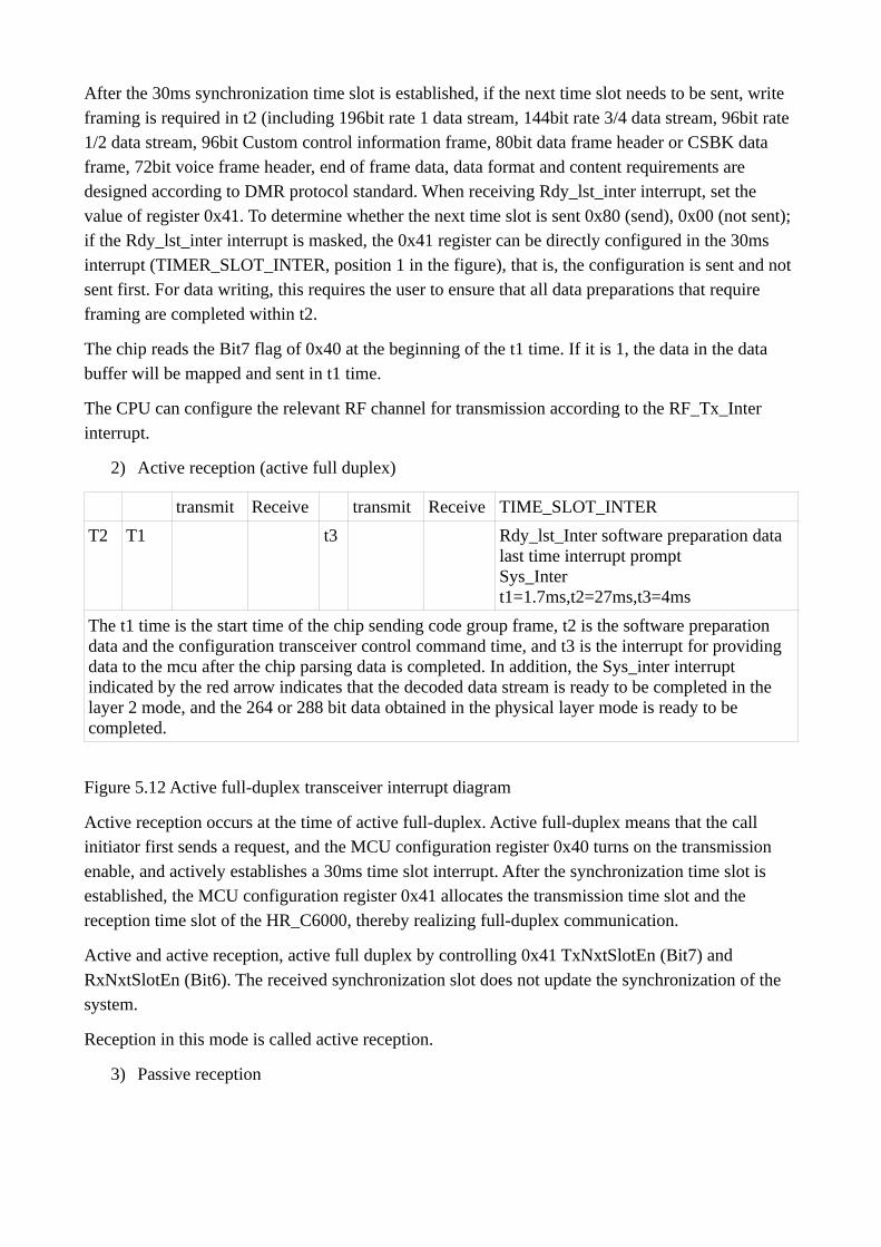
2) Active reception (active full duplex)
transmit Receive transmit Receive TIME_SLOT_INTER
T2 T1 t3 Rdy_lst_Inter software preparation data last time interrupt promptSys_Intert1=1.7ms,t2=27ms,t3=4ms
The t1 time is the start time of the chip sending code group frame, t2 is the software preparation data and the configuration transceiver control command time, and t3 is the interrupt for providing data to the mcu after the chip parsing data is completed. In addition, the Sys_inter interrupt indicated by the red arrow indicates that the decoded data stream is ready to be completed in the layer 2 mode, and the 264 or 288 bit data obtained in the physical layer mode is ready to be completed.
Figure 5.12 Active full-duplex transceiver interrupt diagram
Active reception occurs at the time of active full-duplex. Active full-duplex means that the call initiator first sends a request, and the MCU configuration register 0x40 turns on the transmission enable, and actively establishes a 30ms time slot interrupt. After the synchronization time slot is established, the MCU configuration register 0x41 allocates the transmission time slot and the reception time slot of the HR_C6000, thereby realizing full-duplex communication.
Active and active reception, active full duplex by controlling 0x41 TxNxtSlotEn (Bit7) and RxNxtSlotEn (Bit6). The received synchronization slot does not update the synchronization of the system.
Reception in this mode is called active reception.
3) Passive reception
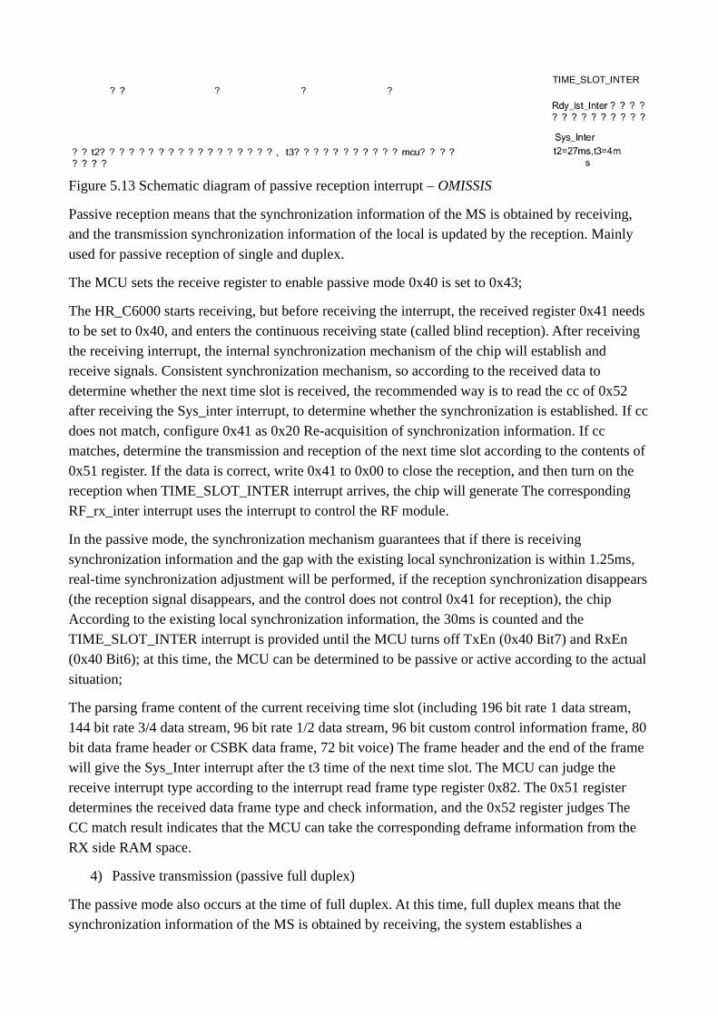
Figure 5.13 Schematic diagram of passive reception interrupt – OMISSIS
Passive reception means that the synchronization information of the MS is obtained by receiving, and the transmission synchronization information of the local is updated by the reception. Mainly used for passive reception of single and duplex.
The MCU sets the receive register to enable passive mode 0x40 is set to 0x43;
The HR_C6000 starts receiving, but before receiving the interrupt, the received register 0x41 needs to be set to 0x40, and enters the continuous receiving state (called blind reception). After receiving the receiving interrupt, the internal synchronization mechanism of the chip will establish and receive signals. Consistent synchronization mechanism, so according to the received data to determine whether the next time slot is received, the recommended way is to read the cc of 0x52 after receiving the Sys_inter interrupt, to determine whether the synchronization is established. If ccdoes not match, configure 0x41 as 0x20 Re-acquisition of synchronization information. If cc matches, determine the transmission and reception of the next time slot according to the contents of 0x51 register. If the data is correct, write 0x41 to 0x00 to close the reception, and then turn on the reception when TIME_SLOT_INTER interrupt arrives, the chip will generate The corresponding RF_rx_inter interrupt uses the interrupt to control the RF module.
In the passive mode, the synchronization mechanism guarantees that if there is receiving synchronization information and the gap with the existing local synchronization is within 1.25ms, real-time synchronization adjustment will be performed, if the reception synchronization disappears(the reception signal disappears, and the control does not control 0x41 for reception), the chip According to the existing local synchronization information, the 30ms is counted and the TIME_SLOT_INTER interrupt is provided until the MCU turns off TxEn (0x40 Bit7) and RxEn (0x40 Bit6); at this time, the MCU can be determined to be passive or active according to the actual situation;
The parsing frame content of the current receiving time slot (including 196 bit rate 1 data stream, 144 bit rate 3/4 data stream, 96 bit rate 1/2 data stream, 96 bit custom control information frame, 80 bit data frame header or CSBK data frame, 72 bit voice) The frame header and the end of the frame will give the Sys_Inter interrupt after the t3 time of the next time slot. The MCU can judge the receive interrupt type according to the interrupt read frame type register 0x82. The 0x51 register determines the received data frame type and check information, and the 0x52 register judges The CC match result indicates that the MCU can take the corresponding deframe information from the RX side RAM space.
4) Passive transmission (passive full duplex)
The passive mode also occurs at the time of full duplex. At this time, full duplex means that the synchronization information of the MS is obtained by receiving, the system establishes a
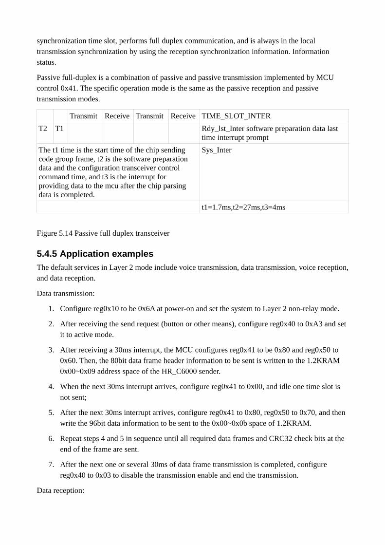
synchronization time slot, performs full duplex communication, and is always in the local transmission synchronization by using the reception synchronization information. Information status.
Passive full-duplex is a combination of passive and passive transmission implemented by MCU control 0x41. The specific operation mode is the same as the passive reception and passive transmission modes.
Transmit Receive Transmit Receive TIME_SLOT_INTER
T2 T1 Rdy_lst_Inter software preparation data last time interrupt prompt
The t1 time is the start time of the chip sending code group frame, t2 is the software preparation data and the configuration transceiver control command time, and t3 is the interrupt for providing data to the mcu after the chip parsing data is completed.
Sys_Inter
t1=1.7ms,t2=27ms,t3=4ms
Figure 5.14 Passive full duplex transceiver
5.4.5 Application examples
The default services in Layer 2 mode include voice transmission, data transmission, voice reception,and data reception.
Data transmission:
1. Configure reg0x10 to be 0x6A at power-on and set the system to Layer 2 non-relay mode.
2. After receiving the send request (button or other means), configure reg0x40 to 0xA3 and set it to active mode.
3. After receiving a 30ms interrupt, the MCU configures reg0x41 to be 0x80 and reg0x50 to 0x60. Then, the 80bit data frame header information to be sent is written to the 1.2KRAM 0x00~0x09 address space of the HR_C6000 sender.
4. When the next 30ms interrupt arrives, configure reg0x41 to 0x00, and idle one time slot is not sent;
5. After the next 30ms interrupt arrives, configure reg0x41 to 0x80, reg0x50 to 0x70, and then write the 96bit data information to be sent to the 0x00~0x0b space of 1.2KRAM.
6. Repeat steps 4 and 5 in sequence until all required data frames and CRC32 check bits at the end of the frame are sent.
7. After the next one or several 30ms of data frame transmission is completed, configure reg0x40 to 0x03 to disable the transmission enable and end the transmission.
Data reception:
1. On power-on, configure reg0x10 to 0x6A and set the system to Layer 2 non-relay mode; reg40 to 0x43 and reg41 to 0x40, and the system is busy.
2. when receiving sys_inter, read reg0x51 and reg0x52, if reg0x51[7:4] is equal to local cc (default is 0x01), and reg0x51[7:4] is equal to 0x06, and reg0x51[2] is equal to 0, then read Take the low 7bit information of the 0x08 address in the receiving RAM, determine the totalnumber of frames to be received next (if the total number of frames to be received is increased by 1), and the address information in the 80 bits in the RAM matches the local address to determine whether it is the data header to be received. ;
3. When the next 30ms interrupt arrives, configure reg0x41 to 0x00. The next time slot is not the received working time slot, and the reception is closed.
4. When the next 30ms interrupt arrives, configure reg0x41 to 0x40. The next time slot is the receive time slot, open the reception, and decrement the number of receptions.
5. repeat 3 and 4 in turn, and the reception is decremented to 0 at this time.
6. In the next 30ms interrupt, configure reg0x41 to 0x40 to be in the busy state again. If you want to turn off reception, configure reg0x40 to 0x03 and reg0x41 to 0x20 and then to 0x00.
In addition, each time sys_inter is received, reg0x52 and reg0x51 are read to determine the state andnature of each frame of data, and the 96-bit data of 0x00~0x0B of the receiving end RAM is read toobtain the content of the received data frame.
Voice transmission:
1. On power-on, configure reg0x10 to 0x6A, set the system to Layer 2 non-relay mode, and register 0x06 to 0x45. The vocoder is controlled by the MCU.
2. After receiving the send request (button or other means), configure reg0x40 to 0xA3 and set it to active mode.
3. After receiving a 30ms interrupt, the MCU configures reg0x41 to be 0x80 and reg0x50 to 0x10. Then, the 80bit voice frame header information to be sent is written to the Tx_buffer 0x00~0x09 address space of the HR_C6000 sender.
4. When the next 30ms interrupt arrives, configure reg0x41 to 0x00, idle one time slot is not sent, and then configure register 0x22 to 0x80 to enable the vocoder code switch.
5. in the next 30ms interrupt is coming, then reg0x41 is configured to 0x80, reg0x50 is configured to 0x08, the next frame is ready to send speech frame A.
6. When the next 30ms interrupt arrives, configure reg0x41 to 0x00, and idle one slot will not be sent.
7. When the next 30ms interrupt arrives, configure reg0x41 to 0x80, reg0x50 to 0x19, and the next frame to send speech frame B.
8. Repeat 6 and 7 in sequence to send the remaining C, D, E, and F frames reg0x50 to 0x2B, 0x3B, 0x4A, and 0x58, respectively.

9. repeat 5~8, keep sending voice frames A, B, C, D, E, F until the button is released, and send all the super frames.
10. Receive a 30ms interrupt at the beginning of the idle time slot, configure reg0x41 to be 0x80, and reg0x50 to 0x20, ready to send the end of the speech frame.
11. When the next 30ms interrupt arrives, when the next 30ms interrupt arrives, configure reg0x41 to 0x00, register 0x22 to 0x40, and the vocoder code is turned off.
12. After the next or a few 30ms of the end of the speech frame is sent, configure reg0x40 to 0x03 to disable the transmission enable and end the transmission.
Voice reception:
1. On power-on, configure reg0x10 to 0x6A and set the system to Layer 2 non-relay mode; reg40 to 0x43 and reg41 to 0x40, and the system is busy.
2. when receiving sys_inter, read reg0x50 and reg0x51, if reg0x51[7:4] is equal to local cc (default is 0x01), and reg0x50[7:4] is equal to 0x01, and reg0x50[2] is equal to 0, and reg0x50 When [1:0] is equal to 0x01, the 0x00~0x08 information in the receive RAM is read. If addrs 0x00 corresponds to a value of 0x00, then match local groupaddrs with addrs0x03~ addrs0x05; if addrs 0x00 corresponds to 0x03, match local srcaddrs with addrs0x03~addrs0x05.
3. When the next 30ms interrupt arrives, configure reg0x41 to 0x00. The next time slot is not the received working time slot. The receiving is closed. If the address matches, the configuration register 0x22 is configured to 0x20, and the vocoder decoding switch is turnedon. .
4. When the next 30ms arrives, configure reg0x41 to 0x50, enable the next time slot to receive enable, and turn on the voice stream output enable to provide the received voice frame to thevocoder output.
5. when the next 30ms arrives, configure reg0x41 to 0x00, the next time slot is not the receivedworking time slot, and the receiving is closed;
6. repeat 4 and 5 until you receive sys_inter, read and read reg0x51. If reg0x51[7:4] is equal to local cc (default is 0x01), and reg0x51[7:4] is equal to 0x01, and reg0x51[2] is equal to 0, and reg0x50[1:0] is equal to 0x02, read receive RAM 0x00~0x08 information. If addrs0x00 has a value of 0x00, then match local groupaddrs with addrs0x03~ addrs0x05; if addrs0x00 has a value of 0x03, match local srcaddrs with addrs0x03~ addrs0x05. If the address matches, the configuration register 0x22 is configured to 0x10, and the vocoder decoding is turned off.
7. For the next 30ms interrupt, configure reg0x41 to 0x40 to be in the busy state again. If you want to turn off reception, configure reg0x40 to 0x03 and reg0x41 to 0x20 and then to 0x00.
5.4.6 Bit error rate test
1. Test Methods:

The HR_C6000 continuously receives 4FSK modulated low IF signals in one layer mode, and the signal frequency is configurable. It is recommended to use 455 kHz or 450 kHz IF signals. HR_C6000 stores the demodulated 36 bytes of data per frame into the interval of the receiving end 1.2KRAM space starting address 0x30. The MCU can read each frame of data from the RAM through the SPI interface and compare it with the 36 bytes of the transmitted data to get the number of error bits of the frame data. The number of error bits per frame of continuous continuous test is accumulated for a long time, and the bit error performance of HR_C6000 is counted.
The data stored in the RAM, the defined data storage structure is shown in Figure 5.15. The MCU can read the frame type (SyncState and SyncClass (0x51)) according to the interrupt, and read the corresponding length data according to the frame type, and parse according to the format. (The data content in the dotted box is to receive additional CACH data in continuous mode).
SlotType20bit
SYNC48bit
Data196bit
SYNC/EMB/RC 48bit
Voice216bit
SYNC48bit
Data48bit
Figure 5.15 Receive Data Frame Type Format
2. Register settings:
Realize the bit error rate test function in one layer mode, the register that needs to be configured is
Realize the bit error rate test function in one layer mode, the registers that need to be configured are Table 5.6 One layer mode error rate test control register address description
Address Configuration value Description
0x01 2’bxxxx 0000 Configured in IF receive mode.
0x07 2’b0000 1011 The IF frequency word is 8 bits high, and the 24-bit IF frequency word is divided by 2^24 by 9.8304M to get the final IF frequency. The default setting is 455kHz.
0x08 2’b1101 1001 8 bits in the IF frequency word.
0x09 2’b0101 0100 The IF frequency word is 8 bits low.
0x10 2’b0000 0010 One layer mode, and continuous reception, if you need time slot reception, you need to configure bit5 to 1.
0x40 2’b0100 0000 Receive enable is enabled and configured as a test mode.
0x41 2’b0100 0001 Receive test enable is enabled.
6 FM applicationThe HR_C6000 is compatible with FM and supports FM transceiver function. The HR_C6000 can work in FM mode by configuring register 0x10[7]=1'b1. The chip is embedded with modules such

as weighting, de-emphasis, compression, and decompression. Users can select the required functions according to their needs. In the transceiver mode, the user can select the 12.5KHz/25KHz channel filter, and in order to prevent excessive modulation, the limiter is embedded in the filter.
Mic_in ADC Compression Aggravation Filter FM modulation Tr_I/Mod1Tr_Q/Mod2
Audio_out Decompression To increase Filter Phase discrimination
Recv_IRecv_Q
Figure 6.1 FM Transceiver Block Diagram
6.1 FM sendIn the analog mode, the HR_C6000 can only work in simplex mode, and the analog transmit channel is opened by configuring register 0x60=0x80. The speech is sampled and converted into a digital signal by the ADC in Codec. After the HR_C6000 internal compression and weighting module performs audio signal processing, it passes through the 12.5KHz/25KHz channel filter to improve the ACPR of the transmitted signal.
The transmission of voice and signaling such as analog voice, analog/digital sub-tone (CTCSS and CDCSS), DTMF, 2-tone/5-tone and MSK is mainly supported on the above analog channels.
Bandpass filter
The HR_C6000 has an optional bandpass filter with a signal bandwidth of 300Hz to 3400Hz. The bandpass filter can be turned on by configuring Register 0x34[7]=1’b1.
Figure 6.2 Bandpass filter spectral response – OMISSIS
Compression
The audio compander consists of a compressor and a decompressor to reduce the effects of noise onaudio quality.
A compressor is used at the transmitting end to reduce the dynamic range of the audio signal by amplifying the small signal and reducing the large signal.
The Syllabic compander is used in the HR_C6000 to change the amplitude of the average envelope of the signal according to the time constant t. The steady-state output of the compressor is the root mean square of the input signal, that is, when the input signal is increased or decreased by 2dB, the output signal is correspondingly increased or decreased by 1dB. Generally, in a voice communication system, the dynamic range can be converted from 60 dB of the input signal to 30 dB of the output signal by audio compression technology. The user can open the compression module by configuring register 0x34[6]=1’b1. It should be noted that the compressor should be used in conjunction with decompression.
OMISSIS
Figure 6.3 Compressed Time Domain Response
At the same time, the user can set the compressor's 0dB compression point by configuring Register 0x2D[3:0].
Aggravation
The HR_C6000 provides an optional weighting module that meets the requirements of the TIA. Theweighting module processes the audio signal in the 300Hz to 3000Hz band at +6dB/Oct. The weighting module can be turned on by configuring register 0x34[5]=1'b1.
OMISSIS
Figure 6.4 Weighted frequency response curve
Filter
The HR_C6000 provides two sets of low-pass filters with embedded soft limiters, 2.55KHz and 3KHz low-pass filters, of which 2.55KHz can be used for 12.5KHz channel spacing to provide better ACPR specifications; 3KHz low The pass filter is typically used for channel spacing of 25KHz. Select by configuration register 0x34.
FM modulation
If the transmit RF interface of the HR_C6000 is configured for baseband IQ or IF mode, FM signal modulation of the audio signal is performed using the FM modulator inside the HR_C6000. The modulation offset is adjusted by configuring 0x3E and Mic gain 0x0F, while preventing overmodulation by configuring the soft limit register 0x3F of the transmit low pass filter.
6.1.1 CTCSS send
The system determines the sub-tone rate (62.5~254.1Hz) according to the set CTCSS sending address code (1~51). The sub-tone signal is generated by querying the sine table. Different

frequencies correspond to different addressing step lengths. The accumulated method sequentially outputs sinusoidal data at a sampling clock rate.
Figure 6.5 CTCSS Transmit Block Diagram – OMISSIS
At the moment the PTT button is released, the audio signal transmission ends, and the subsonic signal phase reversals and continues to remain in the air for approximately 155ms to ensure sufficient voice path closure processing time at the receiving end. Among them, the inversion of the subsonic phase is realized by the above-mentioned sinusoidal table addressing phase jump.
The subsonic signal is weighted by the modulation coefficient (which can be configured by software) and superimposed with the audio signal, and then modulated by FM.
The detailed usage is detailed in Appendix A2.2.1.
6.1.2 CDCSS send
The transmitter first transmits the original data 12-bit via the golay coding cycle to the 23-bit DCS code, then the DCS code is NRZ(1) mapped, and the two-stage interpolated and filtered data is input to the FM modulator to obtain the modulation phase value and the baseband modulation to form the CDCSS. Baseband signal output.
Figure 6.6 Transmitter system block diagram
Detailed usage is detailed in Appendix A2.2.2.
6.1.3 DTMF sending
The DTMF signal is generated by a combination of four sets of high frequency signals and four setsof low frequency signals. The low frequency signal is 2.5 dB lower than the amplitude of the high frequency signal. The DTMF signal is sent before the start of the audio signal, after the PTT is valid, and under normal circumstances, from the PTT press to the transmission of the DTMF signal,there is an idle state of about 600ms in the middle, in order to allow the receiver to have enough time to enter Detection mode.
Flow Description:
Like CTCSS, DTMF signals are also generated by querying a sine table. The high frequency signal is superimposed with the low frequency signal and weighted by the modulation frequency offset coefficient, which is modulated by FM and output. Each DTMF code corresponds to a signal length of 50ms, followed by an IDLE state of 50ms. The length of the code that DTMF can support is determined by the user.
OMISSIS
Figure 6.7 DTMF Transmit Block Diagram
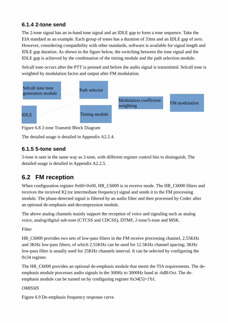
6.1.4 2-tone send
The 2-tone signal has an in-band tone signal and an IDLE gap to form a tone sequence. Take the EIA standard as an example. Each group of tones has a duration of 33ms and an IDLE gap of zero. However, considering compatibility with other standards, software is available for signal length andIDLE gap duration. As shown in the figure below, the switching between the tone signal and the IDLE gap is achieved by the combination of the timing module and the path selection module.
Selcall tone occurs after the PTT is pressed and before the audio signal is transmitted. Selcall tone isweighted by modulation factor and output after FM modulation.
Figure 6.8 2-tone Transmit Block Diagram
The detailed usage is detailed in Appendix A2.2.4.
6.1.5 5-tone send
5-tone is sent in the same way as 2-tone, with different register control bits to distinguish. The detailed usage is detailed in Appendix A2.2.5.
6.2 FM receptionWhen configuration register 0x60=0x00, HR_C6000 is in receive mode. The HR_C6000 filters and receives the received IQ (or intermediate frequency) signal and sends it to the FM processing module. The phase-detected signal is filtered by an audio filter and then processed by Codec after an optional de-emphasis and decompression module.
The above analog channels mainly support the reception of voice and signaling such as analog voice, analog/digital sub-tone (CTCSS and CDCSS), DTMF, 2-tone/5-tone and MSK.
Filter
HR_C6000 provides two sets of low-pass filters in the FM receive processing channel, 2.55KHz and 3KHz low-pass filters, of which 2.55KHz can be used for 12.5KHz channel spacing; 3KHz low-pass filter is usually used for 25KHz channels interval. It can be selected by configuring the 0x34 register.
The HR_C6000 provides an optional de-emphasis module that meets the TIA requirements. The de-emphasis module processes audio signals in the 300Hz to 3000Hz band at -6dB/Oct. The de-emphasis module can be turned on by configuring register 0x34[5]=1'b1.
OMISSIS
Figure 6.9 De-emphasis frequency response curve
Selcall tone tonegeneration module
IDLE
Path selector
Timing module
FM modulationModulation coefficientweighting
Decompression
A decompressor is used at the receiving end to increase the dynamic range of the audio signal by reducing the large signal and amplifying the small signal.
The steady-state output of the decompressor is the square of the input signal, that is, when the input signal is increased or decreased by 1dB, the output signal is correspondingly increased or decreased by 2dB. Generally, in a voice communication system, the dynamic range can be converted from 30 dB of the input signal to 60 dB of the output signal by audio compression technology. The user can open the compression module by configuring register 0x34[6]=1’b1.
OMISSIS
Figure 6.10 Decompressing the time domain response
At the same time, the user can set the compressor's 0dB compression point by configuring Register 0x2D[7:4].
Bandpass filter
The HR_C6000 has an optional bandpass filter built into the FM receiver. The signal bandwidth is 300Hz to 3400Hz. The bandpass filter can be turned on by configuring the register 0x34[7]=1’b1.
6.2.1 CTCSS reception
The CTCSS air signal generates phase information through the phase detector, and the DC offset of the signal is cancelled by the frequency offset calibration module. After the limiting processing, the high frequency audio portion is filtered by the 4th order IIR 300Hz low pass filter.
The frequency response amplitude detection result is compared with the preset threshold value. When the threshold is greater than the threshold, the voice enable is enabled, and the output interrupt signal is sent to the peripheral to open the speaker and the voice path.
OMISSIS
Figure 6.11 CTCSS Receive Block Diagram
Detailed usage is detailed in Appendix A2.2.1.
6.2.2 CDCSS reception
The CDCSS modulation consists of an FM demodulation module that uses a non-coherent demodulation scheme. CDCSS signal reception includes key steps such as differential phase discrimination, frequency offset estimation, decision, and golay decoding. The flow of back-end baseband processing is shown in Figure 6.12.
OMISSIS
Figure 6.12 Receive Baseband Processing Flowchart
The CDCSS baseband signal is filtered by a low-pass filter to remove some of the out-of-band noiseand reduced to an amplitude value by FM demodulation. Then the next two LPFs further filter out the noise and audio signals and then perform frequency offset compensation. The signal obtained at
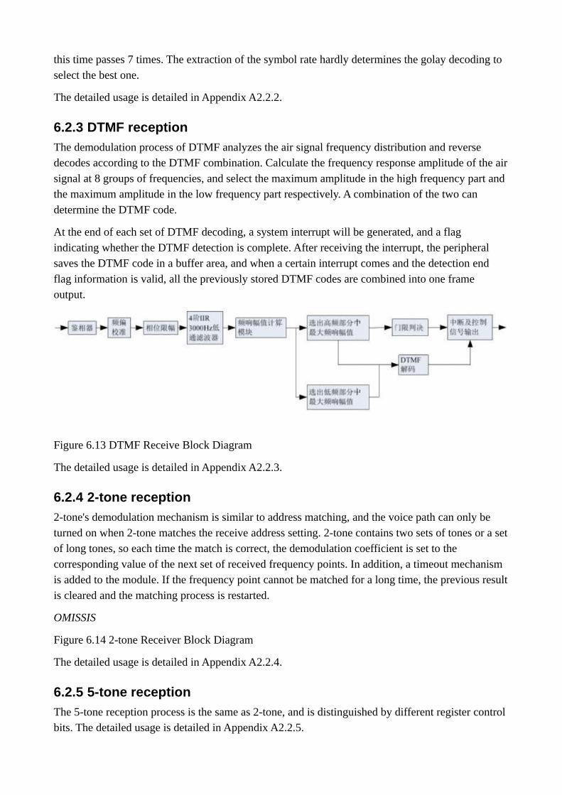
this time passes 7 times. The extraction of the symbol rate hardly determines the golay decoding to select the best one.
The detailed usage is detailed in Appendix A2.2.2.
6.2.3 DTMF reception
The demodulation process of DTMF analyzes the air signal frequency distribution and reverse decodes according to the DTMF combination. Calculate the frequency response amplitude of the airsignal at 8 groups of frequencies, and select the maximum amplitude in the high frequency part and the maximum amplitude in the low frequency part respectively. A combination of the two can determine the DTMF code.
At the end of each set of DTMF decoding, a system interrupt will be generated, and a flag indicating whether the DTMF detection is complete. After receiving the interrupt, the peripheral saves the DTMF code in a buffer area, and when a certain interrupt comes and the detection end flag information is valid, all the previously stored DTMF codes are combined into one frame output.
Figure 6.13 DTMF Receive Block Diagram
The detailed usage is detailed in Appendix A2.2.3.
6.2.4 2-tone reception
2-tone's demodulation mechanism is similar to address matching, and the voice path can only be turned on when 2-tone matches the receive address setting. 2-tone contains two sets of tones or a setof long tones, so each time the match is correct, the demodulation coefficient is set to the corresponding value of the next set of received frequency points. In addition, a timeout mechanism is added to the module. If the frequency point cannot be matched for a long time, the previous resultis cleared and the matching process is restarted.
OMISSIS
Figure 6.14 2-tone Receiver Block Diagram
The detailed usage is detailed in Appendix A2.2.4.
6.2.5 5-tone reception
The 5-tone reception process is the same as 2-tone, and is distinguished by different register control bits. The detailed usage is detailed in Appendix A2.2.5.
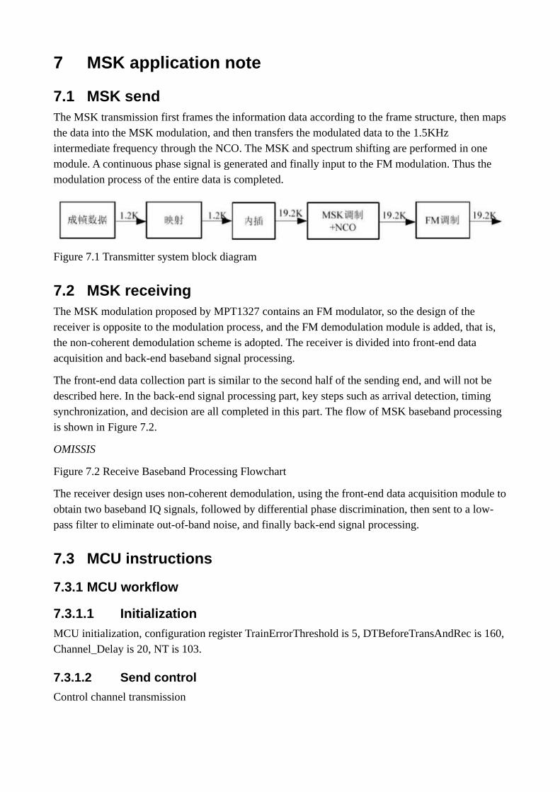
7 MSK application note
7.1 MSK sendThe MSK transmission first frames the information data according to the frame structure, then mapsthe data into the MSK modulation, and then transfers the modulated data to the 1.5KHz intermediate frequency through the NCO. The MSK and spectrum shifting are performed in one module. A continuous phase signal is generated and finally input to the FM modulation. Thus the modulation process of the entire data is completed.
Figure 7.1 Transmitter system block diagram
7.2 MSK receivingThe MSK modulation proposed by MPT1327 contains an FM modulator, so the design of the receiver is opposite to the modulation process, and the FM demodulation module is added, that is, the non-coherent demodulation scheme is adopted. The receiver is divided into front-end data acquisition and back-end baseband signal processing.
The front-end data collection part is similar to the second half of the sending end, and will not be described here. In the back-end signal processing part, key steps such as arrival detection, timing synchronization, and decision are all completed in this part. The flow of MSK baseband processing is shown in Figure 7.2.
OMISSIS
Figure 7.2 Receive Baseband Processing Flowchart
The receiver design uses non-coherent demodulation, using the front-end data acquisition module toobtain two baseband IQ signals, followed by differential phase discrimination, then sent to a low-pass filter to eliminate out-of-band noise, and finally back-end signal processing.
7.3 MCU instructions
7.3.1 MCU workflow
7.3.1.1 Initialization
MCU initialization, configuration register TrainErrorThreshold is 5, DTBeforeTransAndRec is 160, Channel_Delay is 20, NT is 103.
7.3.1.2 Send control
Control channel transmission
