hr1203 - monolithic power
TRANSCRIPT
HR1203 High-Performance
Digital PFC + LLC Combo Controller with Programmable Noise Suppression Filter
HR1203 Rev 1.1 www.MonolithicPower.com 1 3/30/2020 MPS Proprietary Information. Patent Protected. Unauthorized Photocopy and Duplication Prohibited. © 2020 MPS. All Rights Reserved.
The Future of Analog IC Technology
DESCRIPTION The HR1203 is a high-performance controller that integrates an advanced, digital, PFC controller and a half-bridge, LLC resonant controller. The HR1203 requires low input power at no-load or ultra-light load, making it compliant with the Energy Using Product Directive (EuP) Lot 6 and Code of Conduct Version 5 Tier 2 specifications.
The PFC of the HR1203 employs a patented average current control scheme, which can operate both in continuous conduction mode (CCM) and discontinuous conduction mode (DCM) according to the instantaneous condition of the input voltage and output load. The IC exhibits excellent efficiency and high power factor (PF) at light load. The performance of the PFC can be optimized by programming multiple parameters through an I2C GUI. Programming can be completed either by the factory or by the customer referring to a detailed user guide.
The half-bridge LLC resonant converter achieves high efficiency with zero-voltage switching (ZVS). The HR1203 implements an adaptive dead-time adjustment (ADTA) function to guarantee ZVS in different load conditions. Additionally, the HR1203 can prevent the LLC converter from operating in capacitive mode, making it more robust and easier to design.
The HR1203 integrates a high-voltage (HV) current source internally for start-up. When the AC input is removed, the HV current source also functions as an X-cap discharger. Such features are helpful to reduce related devices, thus reduce power consumption at no load.
In order to improve the noise immunity, HR1203 implements multiple programmable digital filters on critical signals.
Full protection features include thermal shutdown, open-loop protection (OLP), over-current protection (OCP), over-voltage protection (OVP), and brown-in/-out protection.
FEATURES General System Features Meets EuP Lot 6 and COC Version 5 Tier 2
Specifications HV Current Source for Start-Up Smart X-Cap Discharger Standard I2C Interface 1k EEPROM to Store Parameters User-Friendly GUI for Digital PFC
PFC Controller High Efficiency from Light Load to Full Load
by CCM/DCM Multi-Mode Control High PF Due to Patented Input Capacitor
Current Compensation Programmable Filter for Noise Suppression Programmable Frequency Jittering Programmable Brown-In and Brown-Out Programmable Soft Start (SS) Cycle-by-Cycle Current Limit Open-Loop Protection (OLP)
LLC Controller
600V High-Side Gate Driver with Integrated Bootstrap Diode and High dV/dt Immunity
Adaptive Dead-Time Adjustment of HB LLC with Minimum and Maximum Limit
Burst Mode Switching Safe Start-Up in Case of System Fault Two-Level Over-Current Protection (OCP) Latch Shutdown Protection Over-Temperature Protection (OTP) Capacitive Mode Protection
APPLICATIONS Notebook Adapters All-in-One or Gaming Power Supply Desktop PC and ATX Power General AC/DC Power Supply up to 600W OLED and Large Format LCD TV Power
Supply
MPS parts are lead-free, halogen-free, and adhere to the RoHS directive. For MPS green status, please visit the MPS website under quality assurance. “MPS” and “The Future of Analog IC Technology” are registered trademarks of Monolithic Power Systems, Inc.
HR1203 – HIGH-PERFORMANCE DIGITAL PFC + LLC COMBO CONTROLLER
HR1203 Rev 1.1 www.MonolithicPower.com 2 3/30/2020 MPS Proprietary Information. Patent Protected. Unauthorized Photocopy and Duplication Prohibited. © 2020 MPS. All Rights Reserved.
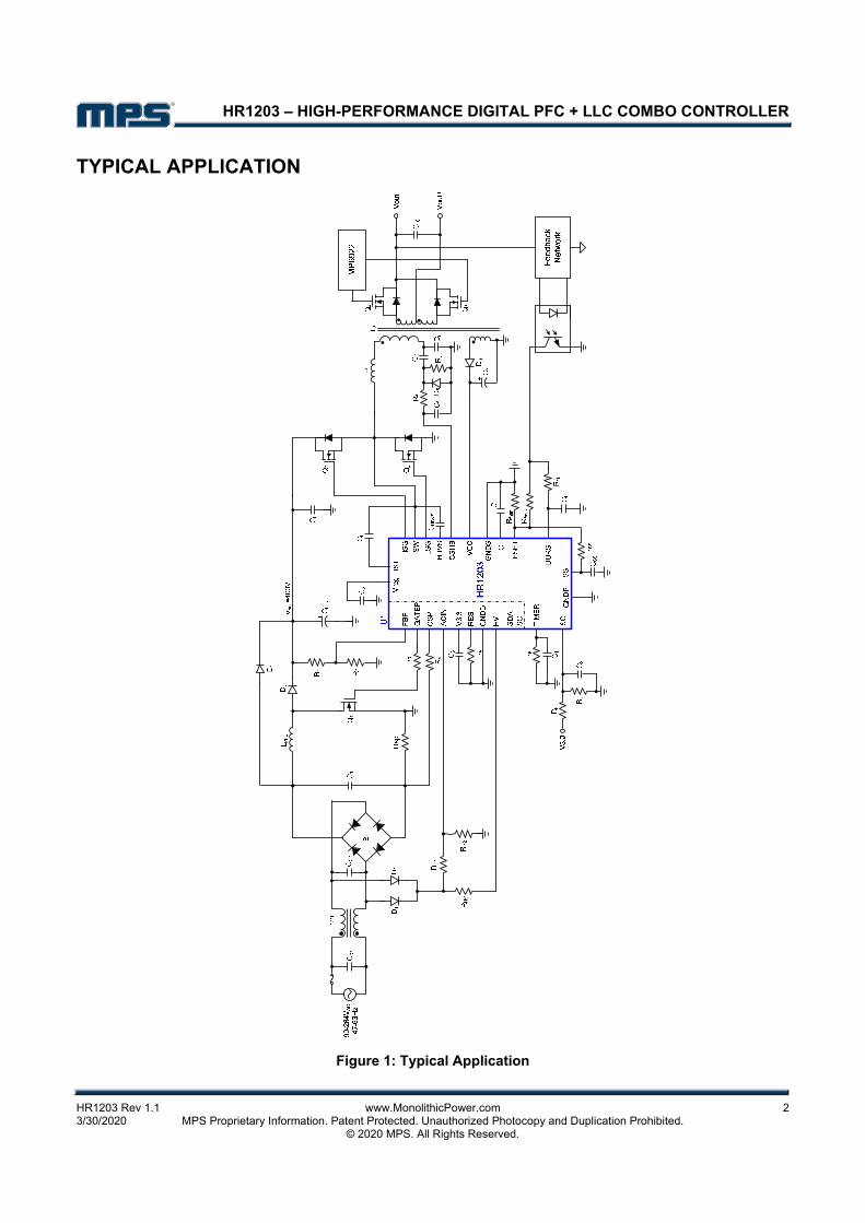
TYPICAL APPLICATION
Figure 1: Typical Application
HR1203 – HIGH-PERFORMANCE DIGITAL PFC + LLC COMBO CONTROLLER
HR1203 Rev 1.1 www.MonolithicPower.com 3 3/30/2020 MPS Proprietary Information. Patent Protected. Unauthorized Photocopy and Duplication Prohibited. © 2020 MPS. All Rights Reserved.
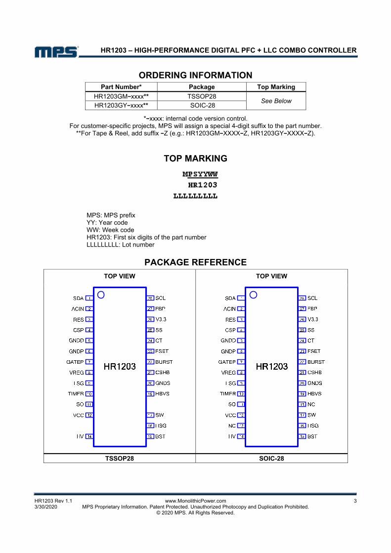
ORDERING INFORMATION Part Number* Package Top Marking
HR1203GM−xxxx** TSSOP28 See Below
HR1203GY−xxxx** SOIC-28
*−xxxx: internal code version control. For customer-specific projects, MPS will assign a special 4-digit suffix to the part number.
**For Tape & Reel, add suffix −Z (e.g.: HR1203GM−XXXX−Z, HR1203GY−XXXX−Z).
TOP MARKING
MPS: MPS prefix YY: Year code WW: Week code HR1203: First six digits of the part number LLLLLLLLL: Lot number
PACKAGE REFERENCE
TOP VIEW TOP VIEW
TSSOP28 SOIC-28
HR1203 – HIGH-PERFORMANCE DIGITAL PFC + LLC COMBO CONTROLLER
HR1203 Rev 1.1 www.MonolithicPower.com 4 3/30/2020 MPS Proprietary Information. Patent Protected. Unauthorized Photocopy and Duplication Prohibited. © 2020 MPS. All Rights Reserved.
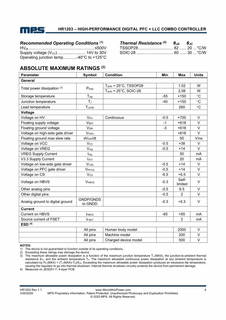
Recommended Operating Conditions (1) HVpk ........................................................... ≤500V Supply voltage (VCC) ......................... 14V to 30V Operating junction temp. ........... -40°C to +125°C
Thermal Resistance (4) θJA θJC TSSOP28 ............................... 82 ...... 20 ... °C/W SOIC-28 ................................. 60 ...... 30 ... °C/W
ABSOLUTE MAXIMUM RATINGS (2)
Parameter Symbol Condition Min Max Units
General
Total power dissipation (3) Ptotal Tamb = 25°C, TSSOP28 1.52 W Tamb = 25°C, SOIC-28 2.08 W
Storage temperature Tstg -55 +150 C
Junction temperature TJ -40 +150 C
Lead temperature TLEAD 260 C
Voltage Voltage on HV VHV Continuous -0.5 +700 V
Floating supply voltage VBST -1 +618 V
Floating ground voltage VSW -3 +618 V Voltage on high-side gate driver VHSG +618 V
Floating ground max slew rate dVSW/dt 50 V/ns Voltage on VCC VCC -0.5 +38 V
Voltage on VREG Vreg -0.5 +14 V
VREG Supply Current Ireg 50 mA
V3.3 Supply Current I3V3 20 mA
Voltage on low-side gate driver VLSG -0.5 +14 V
Voltage on PFC gate driver VPFCG -0.5 +14 V
Voltage on CS VCS -6.5 +6.5 V
Voltage on HBVS VHBVS
-0.3 Self-
limitedV
Other analog pins -0.5 6.5 V
Other digital pins -0.5 2 V
Analog ground to digital ground GNDP/GNDS
to GNDD
-0.3 +0.3 V
Current Current on HBVS IHBVS -65 +65 mA
Source current of FSET IFSET 2 mA
ESD (4) All pins Human body model 2000 V
All pins Machine model 200 V
All pins Charged device model 500 V
NOTES: 1) The device is not guaranteed to function outside of its operating conditions. 2) Exceeding these ratings may damage the device. 3) The maximum allowable power dissipation is a function of the maximum junction temperature TJ (MAX), the junction-to-ambient thermal
resistance θJA, and the ambient temperature TA. The maximum allowable continuous power dissipation at any ambient temperature is calculated by PD (MAX) = (TJ (MAX)-TA)/θJA. Exceeding the maximum allowable power dissipation produces an excessive die temperature, causing the regulator to go into thermal shutdown. Internal thermal shutdown circuitry protects the device from permanent damage.
4) Measured on JESD51-7, 4-layer PCB.

HR1203 – HIGH-PERFORMANCE DIGITAL PFC + LLC COMBO CONTROLLER
HR1203 Rev 1.1 www.MonolithicPower.com 5 3/30/2020 MPS Proprietary Information. Patent Protected. Unauthorized Photocopy and Duplication Prohibited. © 2020 MPS. All Rights Reserved.
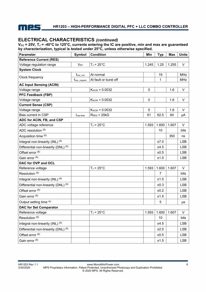
ELECTRICAL CHARACTERISTICS VCC = 25V, TJ = -40°C to 125°C, currents entering the IC are positive, min and max are guaranteed by characterization, typical is tested under 25°C, unless otherwise specified.
Parameter Symbol Condition Min Typ Max Units
High-Voltage Start-Up Current Source (HV)
Breakdown voltage VHVBR 700 V
Normal charge current IHVNOR VHV = 100V, VCC = 15V, TJ = 25°C 5.5 7 8.5 mA
VHV = 100V, VCC = 15V 4.5 7 8.9 mA
Supply current when fault occurs IHVLimit VHV = 100V, VCC = 0V 0.8 1.4 2.1 mA
Leakage current when turned off IHVoff VHV = 400V, VCC = 24V 7 10 µA
IC Power Supply (VCC)
IC turn-on threshold voltage when HV is detected
VCCON(HV) VHV > VHVON 20 21.5 23.1 V
UV protection threshold 1 VCCUVP1 LLC operation 10.5 11.3 12.1 V
UV protection threshold 2 (5) VCCUVP2 LLC disabled 13.9 15 16.2 V
IC release threshold VCCRST 8.4 9 9.9 V
Operation current at normal ICC(nor) RRES =20kΩ, fPFC = 120kHz, fLLC = 200kHz
14 mA
Start-up current ICC-start1 VCC = 20V 0.55 0.7 mA
Current at fault (LLC fault, PFC operation) (5)
ICC-Disable1 TIMER = 4V, PFC burst 4 mA
Current at fault (LLC fault, PFC fault) (5)
ICC-Disable2 TIMER = 4V 0.5 mA
Regulated Power Supply (VREG)
Regulated output voltage Vreg Ireg = 0mA 11 12 12.8 V
Ireg = 30mA 10.8 11.8 12.6 V
IC enable threshold VregON 10.2 10.8 11.5 V
UVP VregUVP 7.7 8.2 8.8 V
Power Supply for Digital Core (V3.3)
Voltage regulation range V3V3 I3V3 = 0mA 2.95 3.15 3.45 V
I3V3 = 15mA 2.85 3.1 3.35 V
X-Cap Discharger (HV)
X-cap discharger current (5) IX-d 5.5 mA
X-cap discharger clock time TX-d 0.9 1.5 2.4 ms
PFC Gate Driver
Sourcing capacity (5) Igate_sr CGate = 1nF 750 mA
Sinking capacity (5) Igate_sk CGate = 1nF -800 mA
Gate-on resistor Ron(H) Sourcing 20mA 4.5 Ω
Ron(L) Sinking 20mA 2.5 Ω
Voltage fall time Tf CGate = 1nF 10 ns
Voltage rise time Tr CGate = 1nF 15 ns
HR1203 – HIGH-PERFORMANCE DIGITAL PFC + LLC COMBO CONTROLLER
HR1203 Rev 1.1 www.MonolithicPower.com 6 3/30/2020 MPS Proprietary Information. Patent Protected. Unauthorized Photocopy and Duplication Prohibited. © 2020 MPS. All Rights Reserved.
ELECTRICAL CHARACTERISTICS (continued) VCC = 25V, TJ = -40°C to 125°C, currents entering the IC are positive, min and max are guaranteed by characterization, typical is tested under 25°C, unless otherwise specified.
Parameter Symbol Condition Min Typ Max Units
Reference Current (RES)
Voltage regulation range VRT TJ = 25°C 1.245 1.25 1.255 V
System Clock
Clock frequency fosc_nor At normal 19 MHz
fosc_nopwm At fault or burst off 1 MHz
AC Input Sensing (ACIN)
Voltage range KACIN = 0.0032 0 1.6 V
PFC Feedback (FBP)
Voltage range KACIN = 0.0032 0 1.6 V
Current Sense (CSP)
Voltage range KACIN = 0.0032 0 1.6 V
Bias current in CSP Icsp-bias RRES = 20kΩ 61 62.5 64 µA
ADC for ACIN, FB, and CSP
ADC voltage reference TJ = 25°C 1.593 1.600 1.607 V
ADC resolution (6) 10 bits
Acquisition time (6) 350 ns
Integral non-linearity (INL) (6) ±7.0 LSB
Differential non-linearity (DNL) (6) ±4.5 LSB
Offset error (6) ±0.5 LSB
Gain error (6) ±1.5 LSB
DAC for OVP and OCL
Reference voltage TJ = 25°C 1.593 1.600 1.607 V
Resolution (6) 7 bits
Integral non-linearity (INL) (6) ±1.5 LSB
Differential non-linearity (DNL) (6) ±0.3 LSB
Offset error (6) ±0.2 LSB
Gain error (6) ±1.5 LSB
Output setting time (6) 5 µs
DAC for Set Comparator
Reference voltage TJ = 25°C 1.593 1.600 1.607 V
Resolution (6) 10 bits
Integral non-linearity (INL) (6) ±4.5 LSB
Differential non-linearity (DNL) (6) ±2.0 LSB
Offset error (6) ±0.5 LSB
Gain error (6) ±1.5 LSB
HR1203 – HIGH-PERFORMANCE DIGITAL PFC + LLC COMBO CONTROLLER
HR1203 Rev 1.1 www.MonolithicPower.com 7 3/30/2020 MPS Proprietary Information. Patent Protected. Unauthorized Photocopy and Duplication Prohibited. © 2020 MPS. All Rights Reserved.
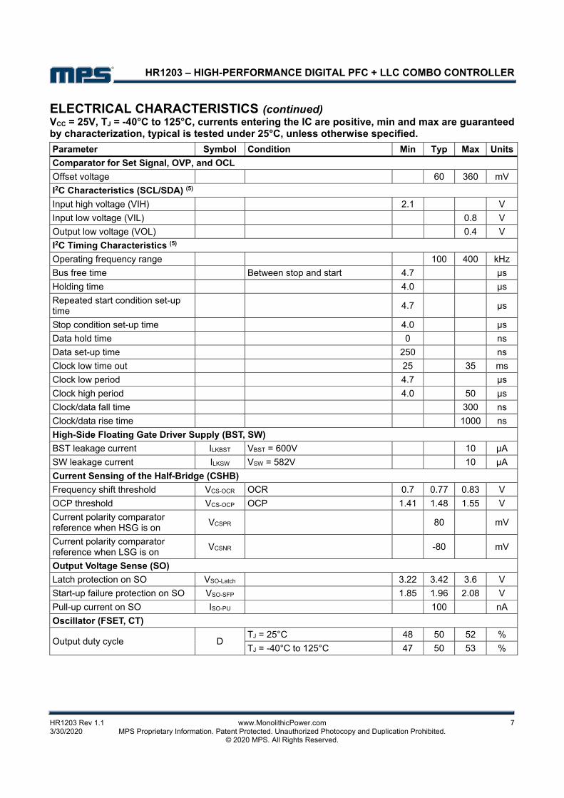
ELECTRICAL CHARACTERISTICS (continued) VCC = 25V, TJ = -40°C to 125°C, currents entering the IC are positive, min and max are guaranteed by characterization, typical is tested under 25°C, unless otherwise specified.
Parameter Symbol Condition Min Typ Max Units
Comparator for Set Signal, OVP, and OCL
Offset voltage 60 360 mV
I2C Characteristics (SCL/SDA) (5)
Input high voltage (VIH) 2.1 V
Input low voltage (VIL) 0.8 V
Output low voltage (VOL) 0.4 V
I2C Timing Characteristics (5)
Operating frequency range 100 400 kHz
Bus free time Between stop and start 4.7 μs
Holding time 4.0 μs
Repeated start condition set-up time
4.7 μs
Stop condition set-up time 4.0 μs
Data hold time 0 ns
Data set-up time 250 ns
Clock low time out 25 35 ms
Clock low period 4.7 μs
Clock high period 4.0 50 μs
Clock/data fall time 300 ns
Clock/data rise time 1000 ns
High-Side Floating Gate Driver Supply (BST, SW)
BST leakage current ILKBST VBST = 600V 10 µA
SW leakage current ILKSW VSW = 582V 10 µA
Current Sensing of the Half-Bridge (CSHB)
Frequency shift threshold VCS-OCR OCR 0.7 0.77 0.83 V
OCP threshold VCS-OCP OCP 1.41 1.48 1.55 V
Current polarity comparator reference when HSG is on
VCSPR 80 mV
Current polarity comparator reference when LSG is on
VCSNR -80 mV
Output Voltage Sense (SO)
Latch protection on SO VSO-Latch 3.22 3.42 3.6 V
Start-up failure protection on SO VSO-SFP 1.85 1.96 2.08 V
Pull-up current on SO ISO-PU 100 nA
Oscillator (FSET, CT)
Output duty cycle D TJ = 25°C 48 50 52 %
TJ = -40°C to 125°C 47 50 53 %
HR1203 – HIGH-PERFORMANCE DIGITAL PFC + LLC COMBO CONTROLLER
HR1203 Rev 1.1 www.MonolithicPower.com 8 3/30/2020 MPS Proprietary Information. Patent Protected. Unauthorized Photocopy and Duplication Prohibited. © 2020 MPS. All Rights Reserved.
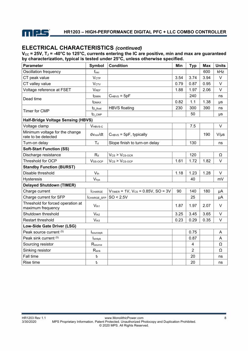
ELECTRICAL CHARACTERISTICS (continued) VCC = 25V, TJ = -40°C to 125°C, currents entering the IC are positive, min and max are guaranteed by characterization, typical is tested under 25°C, unless otherwise specified.
Parameter Symbol Condition Min Typ Max Units
Oscillation frequency fosc 600 kHz
CT peak value VCTP 3.54 3.74 3.94 V
CT valley value VCTV 0.79 0.87 0.95 V
Voltage reference at FSET VREF 1.88 1.97 2.06 V
Dead time tDMIN CHBVS = 5pF 240 ns
tDMAX 0.82 1.1 1.38 µs
Timer for CMP tD_float HBVS floating 230 300 390 ns
tD_CMP 50 µs
Half-Bridge Voltage Sensing (HBVS)
Voltage clamp VHBVS-C 7.5 V
Minimum voltage for the change rate to be detected
dvmin/dt CHBVS = 5pF, typically 190 V/µs
Turn-on delay Td Slope finish to turn-on delay 130 ns
Soft-Start Function (SS)
Discharge resistance Rd VCS > VCS-OCR 120 Ω
Threshold for OCP VSS-OCP VCS > VCS-OCP 1.61 1.72 1.82 V
Standby Function (BURST)
Disable threshold Vth 1.18 1.23 1.28 V
Hysteresis Vhys 40 mV
Delayed Shutdown (TIMER)
Charge current ICHARGE VTIMER = 1V, VCS = 0.85V, SO = 3V 90 140 180 µA
Charge current for SFP ICHARGE_SFP SO < 2.5V 25 µA
Threshold for forced operation at maximum frequency
Vth1 1.87 1.97 2.07 V
Shutdown threshold Vth2 3.25 3.45 3.65 V
Restart threshold Vth3 0.23 0.29 0.35 V
Low-Side Gate Driver (LSG)
Peak source current (5) Isourcepk 0.75 A
Peak sink current (5) Isinkpk 0.87 A
Sourcing resistor Rsource 4 Ω
Sinking resistor Rsink 2 Ω
Fall time tf 20 ns
Rise time tr 20 ns

HR1203 – HIGH-PERFORMANCE DIGITAL PFC + LLC COMBO CONTROLLER
HR1203 Rev 1.1 www.MonolithicPower.com 9 3/30/2020 MPS Proprietary Information. Patent Protected. Unauthorized Photocopy and Duplication Prohibited. © 2020 MPS. All Rights Reserved.
ELECTRICAL CHARACTERISTICS (continued) VCC = 25V, TJ = -40°C to 125°C, currents entering the IC are positive, min and max are guaranteed by characterization, typical is tested under 25°C, unless otherwise specified.
Parameter Symbol Condition Min Typ Max Units
High-Side Gate Driver (HSG, Referenced to SW)
Peak source current (5) Isourcepk 0.74 A
Peak sink current (5) Isinkpk 0.87 A
Sourcing resistor Rsource 4 Ω
Sinking resistor Rsink 2 Ω
Fall time tf 20 ns
Rise time tr 20 ns
Thermal Shutdown
Thermal shutdown threshold 145 °C
Thermal shutdown recovery threshold
100 °C
NOTES: 5) Guaranteed by design. 6) Guaranteed by characterization.

HR1203 – HIGH-PERFORMANCE DIGITAL PFC + LLC COMBO CONTROLLER
HR1203 Rev 1.1 www.MonolithicPower.com 10 3/30/2020 MPS Proprietary Information. Patent Protected. Unauthorized Photocopy and Duplication Prohibited. © 2020 MPS. All Rights Reserved.
TYPICAL CHARACTERISTICS
10
12
14
16
18
20
22
24
-50 0 50 100 150
2
1.2
1.4
1.6
1.8
2
2
5
8
11
2
2.5
3
3.5
4
200
400
600
800
1000
0
1
2
3
4
5
VCC On
VCC UVP
OVP DACOCL DAC
Set DAC
3V3
VREG
SFP
Latch
Fixed DT Min DT
Max DT
CT Peak
CT Valley
-50 0 50 100 150 -50 0 50 100 150
-50 0 50 100 150 -50 0 50 100 150 -50 0 50 100 150
-50 0 50 100 150 -50 0 50 100 150 -50 0 50 100 150
61
62
63
64
1.1
1.2
1.3
1.4

HR1203 – HIGH-PERFORMANCE DIGITAL PFC + LLC COMBO CONTROLLER
HR1203 Rev 1.1 www.MonolithicPower.com 11 3/30/2020 MPS Proprietary Information. Patent Protected. Unauthorized Photocopy and Duplication Prohibited. © 2020 MPS. All Rights Reserved.
TYPICAL CHARACTERISTICS (continued)
HR1203 – HIGH-PERFORMANCE DIGITAL PFC + LLC COMBO CONTROLLER
HR1203 Rev 1.1 www.MonolithicPower.com 12 3/30/2020 MPS Proprietary Information. Patent Protected. Unauthorized Photocopy and Duplication Prohibited. © 2020 MPS. All Rights Reserved.
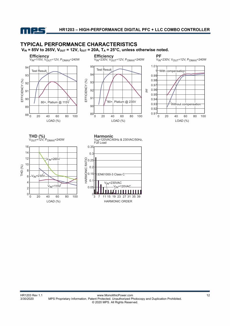
TYPICAL PERFORMANCE CHARACTERISTICS VIN = 85V to 265V, VOUT = 12V, IOUT = 20A, TA = 25°C, unless otherwise noted.
88
89
90
91
92
93
94
0 20 40 60 80 10089
90
91
92
93
94
95
0 20 40 60 80 1000.91
0.92
0.93
0.94
0.95
0.96
0.97
0.98
0.99
1
1.01
0 20 40 60 80 100
0
2
4
6
8
10
12
14
16
0 20 40 60 80 1000
0.05
0.1
0.15
0.2
0.25
0.3
0.35
3 7 11 15 19 23 27 31 35 39
Test Result Test Result
Without compensation
With compensation
VIN=120VACVIN=230VAC
EN61000-3 Class C

HR1203 – HIGH-PERFORMANCE DIGITAL PFC + LLC COMBO CONTROLLER
HR1203 Rev 1.1 www.MonolithicPower.com 13 3/30/2020 MPS Proprietary Information. Patent Protected. Unauthorized Photocopy and Duplication Prohibited. © 2020 MPS. All Rights Reserved.
TYPICAL PERFORMANCE CHARACTERISTICS (continued) VIN = 85V to 265V, VOUT = 12V, IOUT = 20A, TA = 25°C, unless otherwise noted.
VIN100V/div.
IIN2A/div.
VIN100V/div.
IIN2A/div. IPFC
2A/div.
IR2A/div.
IPFC2A/div.
IR2A/div.
IR2A/div.
IR2A/div.
VLG5V/div.
VSW100V/div.
VHG5V/div.
VOUT5V/div.
VBUS100V/div.
IPFC5A/div.
IR2A/div.
VOUT5V/div.
VBUS100V/div.
IPFC5A/div.
IR2A/div.
VOUT5V/div.
VBUS100V/div.
IPFC5A/div.
VHG5V/div.
VLG5V/div.
VSW100V/div.
IR2A/div.

HR1203 – HIGH-PERFORMANCE DIGITAL PFC + LLC COMBO CONTROLLER
HR1203 Rev 1.1 www.MonolithicPower.com 14 3/30/2020 MPS Proprietary Information. Patent Protected. Unauthorized Photocopy and Duplication Prohibited. © 2020 MPS. All Rights Reserved.
TYPICAL PERFORMANCE CHARACTERISTICS (continued) VIN = 85V to 265V, VOUT = 12V, IOUT = 20A, TA = 25°C, unless otherwise noted.
VLG5V/div.
VSW100V/div.
VHG5V/div.
VHBVS2V/div.
VCS1V/div.
VSO2V/div.
VTIMER1V/div.
VCC5V/div.
VCS1V/div.
VSO2V/div.
VTIMER1V/div.
VCC5V/div.
VOUTAC Coupled500mV/div.
VBUS100V/div.
IR2A/div.
IPFC2A/div.
VOUTAC Coupled500mV/div.
VBUS100V/div.
IR2A/div.
IPFC2A/div.
VOUT5V/div.
VSO1V/div.
VTIMER1V/div.
VSO2V/div.
VCC5V/div.
VTIMER1V/div.
IR5A/div.
VSW100V/div.
VLG5V/div.
IR2A/div.
VHG to GND100V/div.

HR1203 – HIGH-PERFORMANCE DIGITAL PFC + LLC COMBO CONTROLLER
HR1203 Rev 1.1 www.MonolithicPower.com 15 3/30/2020 MPS Proprietary Information. Patent Protected. Unauthorized Photocopy and Duplication Prohibited. © 2020 MPS. All Rights Reserved.
PIN FUNCTIONS
Package Pin #
Name Description
1 SDA I2C data bus. Connect a suitable pull-up resistor from SDA to V3.3.
2 ACIN
Input voltage sensing. ACIN is connected to ADC internally. The voltage is used for on-time calculation and brown-in/brown-out protection. The ratio of the external resistor divider should be 0.0032. It is recommended to connect a 680pF capacitorfrom ACIN to GNDD.
3 RES Reference current for producing system clock and bias voltage on CSP. RES connects to a precise reference voltage of 1.25V internally. The reference current is produced by connecting a 20kΩ, 0.5% resistor externally from RES to GNDD.
4 CSP Sensing of the PFC inductor current. Connect a 20kΩ, 0.5% resistor to CS to produce a bias voltage of 1.25V.
5 GNDD Ground reference for the digital core of the PFC.
6 GNDP Ground reference of the PFC gate driver and the LLC low-side gate driver.
7 GATEP Gate driver output of the PFC MOSFET.
8 VREG Regulated power supply. VREG provides a regulated power supply for the PFC and LLC gate drivers or external circuits.
9 LSG Low-side gate driver of HB. The driver is capable of a minimum 0.7A sourcingcurrent and a minimum 0.8A peak sinking current to drive the lower MOSFET of the half-bridge leg. LSG is tied to GND actively during UVLO.
10 TIMER Setting of protection and recovery time. Connect a capacitor and a resistor from TIMER to GNDS to set both over-current protection delay and recovery delay.
11 SO
Latch protection and start-up failure protection. If the SO voltage exceeds VSO-
Latch, the IC stops switching immediately and remains latched off until VCC drops below VCCRST. When the LLC is enabled during start-up, if the SO voltage is still below VSO-SFP after the TIMER voltage reaches Vth2, the IC stops operating. Connect SO and GNDS with a noise-decoupling capacitor higher than 100nF in value placed as close to the IC as possible.
12 VCC IC supply power. When the power is on, VCC is charged up by HVCS initially, and then is charged up by the auxiliary power supply.
13, 18 NC Not connected. NC is not connected in the SOIC-28 package and removed in TSSOP28 package to increase creepage distance.
14 HV High-voltage current source for the IC start-up. HV also acts as an X-capdischarger when the input voltage drops out.
15 BST Voltage bootstrap. BST is connected externally to a capacitor to build a power supply to drive the high-side MOSFET of the HB LLC.
16 HSG High-side gate driver of HB. HSG is the gate driver output for the high-side MOSFET of the HB LLC.
17 SW Reference of the high-side gate driver and bootstrap capacitor.
19 HBVS
Slope sensing to achieve adaptive dead-time adjustment. HBVS detects the dV/dt of the half-bridge mid-point. A 5pF high-voltage capacitor is recommended to be placed between SW and HBVS. LLC works with fixed dead-time (about 300ns) when HBVS is floating. Connecting HBVS to GNDS disables the LLC switching.
20 GNDS Ground reference of LLC and power management circuits.
HR1203 – HIGH-PERFORMANCE DIGITAL PFC + LLC COMBO CONTROLLER
HR1203 Rev 1.1 www.MonolithicPower.com 16 3/30/2020 MPS Proprietary Information. Patent Protected. Unauthorized Photocopy and Duplication Prohibited. © 2020 MPS. All Rights Reserved.
PIN FUNCTIONS (continued)
Package Pin #
Name Description
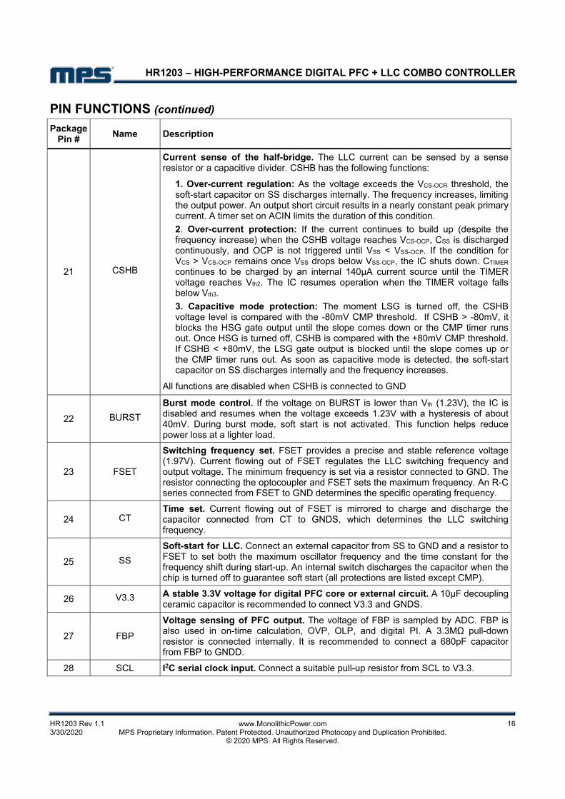
21 CSHB
Current sense of the half-bridge. The LLC current can be sensed by a sense resistor or a capacitive divider. CSHB has the following functions:
1. Over-current regulation: As the voltage exceeds the VCS-OCR threshold, the soft-start capacitor on SS discharges internally. The frequency increases, limiting the output power. An output short circuit results in a nearly constant peak primary current. A timer set on ACIN limits the duration of this condition.
2. Over-current protection: If the current continues to build up (despite the frequency increase) when the CSHB voltage reaches VCS-OCP, CSS is discharged continuously, and OCP is not triggered until VSS < VSS-OCP. If the condition for VCS > VCS-OCP remains once VSS drops below VSS-OCP, the IC shuts down. CTIMER
continues to be charged by an internal 140µA current source until the TIMERvoltage reaches Vth2. The IC resumes operation when the TIMER voltage falls below Vth3.
3. Capacitive mode protection: The moment LSG is turned off, the CSHB voltage level is compared with the -80mV CMP threshold. If CSHB > -80mV, it blocks the HSG gate output until the slope comes down or the CMP timer runsout. Once HSG is turned off, CSHB is compared with the +80mV CMP threshold. If CSHB < +80mV, the LSG gate output is blocked until the slope comes up or the CMP timer runs out. As soon as capacitive mode is detected, the soft-start capacitor on SS discharges internally and the frequency increases.
All functions are disabled when CSHB is connected to GND
22 BURST
Burst mode control. If the voltage on BURST is lower than Vth (1.23V), the IC is disabled and resumes when the voltage exceeds 1.23V with a hysteresis of about 40mV. During burst mode, soft start is not activated. This function helps reduce power loss at a lighter load.
23 FSET
Switching frequency set. FSET provides a precise and stable reference voltage(1.97V). Current flowing out of FSET regulates the LLC switching frequency and output voltage. The minimum frequency is set via a resistor connected to GND. The resistor connecting the optocoupler and FSET sets the maximum frequency. An R-C series connected from FSET to GND determines the specific operating frequency.
24 CT Time set. Current flowing out of FSET is mirrored to charge and discharge the capacitor connected from CT to GNDS, which determines the LLC switching frequency.
25 SS
Soft-start for LLC. Connect an external capacitor from SS to GND and a resistor to FSET to set both the maximum oscillator frequency and the time constant for the frequency shift during start-up. An internal switch discharges the capacitor when the chip is turned off to guarantee soft start (all protections are listed except CMP).
26 V3.3 A stable 3.3V voltage for digital PFC core or external circuit. A 10µF decoupling ceramic capacitor is recommended to connect V3.3 and GNDS.
27 FBP
Voltage sensing of PFC output. The voltage of FBP is sampled by ADC. FBP is also used in on-time calculation, OVP, OLP, and digital PI. A 3.3MΩ pull-down resistor is connected internally. It is recommended to connect a 680pF capacitor from FBP to GNDD.
28 SCL I2C serial clock input. Connect a suitable pull-up resistor from SCL to V3.3.
HR1203 – HIGH-PERFORMANCE DIGITAL PFC + LLC COMBO CONTROLLER
HR1203 Rev 1.1 www.MonolithicPower.com 17 3/30/2020 MPS Proprietary Information. Patent Protected. Unauthorized Photocopy and Duplication Prohibited. © 2020 MPS. All Rights Reserved.
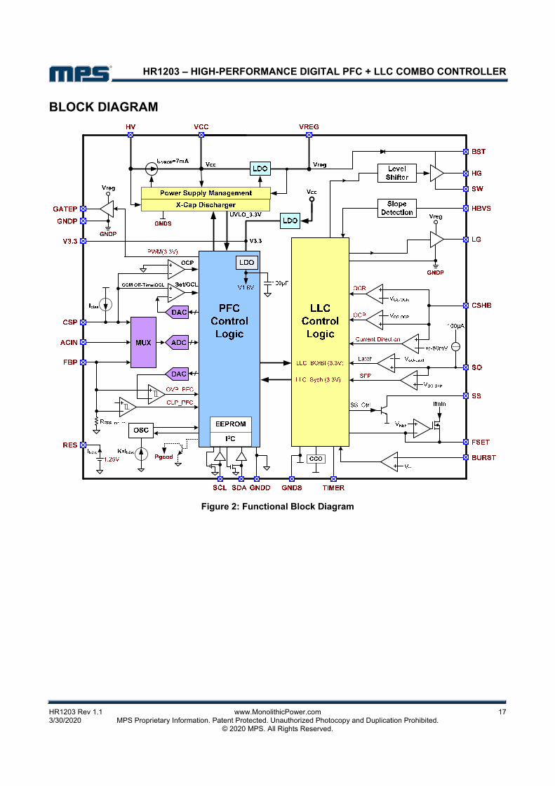
BLOCK DIAGRAM
Figure 2: Functional Block Diagram

HR1203 – HIGH-PERFORMANCE DIGITAL PFC + LLC COMBO CONTROLLER
HR1203 Rev 1.1 www.MonolithicPower.com 18 3/30/2020 MPS Proprietary Information. Patent Protected. Unauthorized Photocopy and Duplication Prohibited. © 2020 MPS. All Rights Reserved.
OPERATION The HR1203 is a high-performance combo controller that integrates digital PFC and HB LLC controllers.
EEPROM
The HR1203 applies an EEPROM as the non-volatile memory (NVM). The EEPROM has 1kb of data memory and 16 bytes of security memory.
There are only two commands used to operate the EEPROM:
1. Read all the data from EEPROM to the memory map. This process operates when it receives a RESTORE_USER_ALL command (51h) from the I2C or operates automatically before the IC runs.
2. Write all the data from the memory map to the EEPROM. This process operates when it receives a STORE_USER_ALL command (50h) from the I2C.
I2C Communication and GUI
The HR1203 has a standard I2C interface. It is recommended to select an I2C tool with 100kHz clock frequency. The I2C can read and write the memory map and send a command to load the data from the EEPROM to the memory map or reload the data from the memory map to the EEPROM with the graphic user interface (GUI) (see Figure 3). For details, please refer to the application notes AN103 “User Guide for the HR1200 I2C Kit and GUI” and AN102 “User Guide for HR1200 Layout” available on the MPS website.
Power Supply Management
This section describes how the HR1203 produces and optimizes the power supply for circuits inside the IC. An optimized power source can reduce no-load consumption and provide robust operation with sufficient fault protection. A high-voltage current source is also integrated in the IC for start-up and X-cap discharge when the AC input drops out.
System Functions
This section describes functions that the HR1203 integrates to improve system performance, including X-cap discharge, IC on/off control, a power good signal, and an interface between the PFC stage and the LLC stage for synchronous operation.
Digital PFC Controller
The HR1203 uses a digital PFC controller that integrates digital logic, ADC, DAC, and comparators to achieve PFC functionality. To acquire programmable design parameters, I2C communication functions and EEPROM are also included.
HB LLC Controller
The HB LLC converter can generate an isolated and regulated output voltage from the high voltage DC bus. With an adaptive dead-time control method, the HB LLC controller helps the converter operate in ZVS in a wider load range, improving the efficiency of the converter at light load. The IC implements anti-capacitive mode operation protection, allowing for robust product design.
Figure 3: HR1203 I2C GUI

HR1203 – HIGH-PERFORMANCE DIGITAL PFC + LLC COMBO CONTROLLER
HR1203 Rev 1.1 www.MonolithicPower.com 19 3/30/2020 MPS Proprietary Information. Patent Protected. Unauthorized Photocopy and Duplication Prohibited. © 2020 MPS. All Rights Reserved.
PART 1: POWER SUPPLY MANAGEMENT
The power supply management function is implemented via four output pins: HV, VCC, VREG, and V3.3. Figure 4 and Figure 5 show the block diagram and operation waveforms of the power management circuit.
Figure 4: Block Diagram of Power Supply
Figure 5: Operation Waveforms of Power Supply
High-Voltage Start-Up Input (HV)
A 7mA current source charges VCC internally when a voltage larger than 40V is applied to HV. If VCC is lower than 1.2V, the charge current from HV is limited to IHVLimit (typically 1.4mA) to prevent excessive power loss caused by a VCC short circuit during start-up.
During normal operation, the voltage on VCC rises quickly after start-up, and the HV current source switches to the nominal current, IHVNOR (typically 7mA). IHVNOR charges the capacitor connected to VCC externally and VCC ramps up. The HV current source is switched off when VCC exceeds the start-up level, VCCON(HV) (typically 21.5V). The HV current source turns
on again when VCC drops below VCCUVP1 (typically 11.3V). Once the HV current source is turned off, the leakage current into HV should be below IHVoff (typically 7µA).
IC Supply Input (VCC)
VCC provides operational power for most of the internal circuits. The IC can start up with the HV start-up current source.
If the start-up current comes from HV when VCC reaches VCCON(HV), the internal LDO is powered on. VREG begins building up, and the IC starts operating if no fault condition occurs. Then VCC is powered by the auxiliary winding of the HBC transformer. Once VCC drops below VCCUVP1, the following actions occur:
The IC stops operating, and the PFC controller stops switching immediately. The HB LLC controller continues to operate until the low-side MOSFET is turned on.
The VREG LDO is disabled.
The HV current source charges VCC until VCC reaches VCCON(HV), then VREG LDO is turned on again. If the IC enters latch mode, the latch status remains until VCC falls below VCCRST.
If VCC supplied by an external DC power source instead of HV current source, please refer to the HR1204 as an alternative.
Regulated Output (VREG)
An internal LDO is added to stabilize the voltage to supply the internal PFC driver, the internal low-side driver of HB LLC, the internal high-side driver of HB LLC via a bootstrap diode, and a reference voltage.
The LDO is enabled only when VCC is higher than VCCON(HV). This ensures that any optional external circuitry connected to VREG does not dissipate any of the start-up current.
The IC starts switching only when VREG is higher than VregON (typically 10.8V). If VREG falls below VregUVP (typically 8.2V), the IC and the PFC controller stop switching immediately. The HB LLC controller continues operating until the low-side MOSFET is turned on.

HR1203 – HIGH-PERFORMANCE DIGITAL PFC + LLC COMBO CONTROLLER
HR1203 Rev 1.1 www.MonolithicPower.com 20 3/30/2020 MPS Proprietary Information. Patent Protected. Unauthorized Photocopy and Duplication Prohibited. © 2020 MPS. All Rights Reserved.
V3.3 for Digital Logic
V3.3 is a stabilized power supply for the internal digital logic. V3.3 is the output of an LDO with its input connected to VCC internally. The output of V3.3 is connected to a digital section with an internal bonding wire. When VCC is larger than VCCRST plus a hysteresis of about 0.5V, the V3.3 LDO is enabled and can be disabled only when VCC is lower than VCCRST.
The capacitor on V3.3 should be in the range of 4.7 - 10µF to guarantee that V3.3 is stable.
Some internal digital circuits are biased off 1.8V, which is powered by an LDO that uses the 3.3V as the input.
UVLO (3.3V Signal)
The under-voltage lockout (UVLO) (3.3V signal) is an enable signal for both the digital PFC and LLC controller. When VCC is larger than VCCUVP1 and VREG is larger than VregON, UVLO (3.3V signal) goes high.
PART 2: SYSTEM FUNCTIONS
X-Cap Discharger
X-caps are critical components placed at the input terminals of the power supply to filter out differential mode EMI noise. If the AC line voltage is removed, the redundant voltage on the X-caps may cause harm to the user. Safety standards require the voltage to be discharged to a safe level within a certain time frame.
Typically, resistors are placed in parallel with X-caps across the AC line to provide a discharge path. Extra resistors bring continuous power consumption as long as the AC input is connected, which is the significant contributor to power consumption at no-load or standby conditions.
The HV current source in the HR1203 acts as a smart X-cap discharger when the AC input is removed. Therefore, traditional discharge resistors can be eliminated. Operating waveforms are shown in Figure 6.
In a normal stage, the HV current source is off. The leakage current in HV is small, so power consumption is reduced significantly. Once the AC voltage is disconnected, after a detection time window (Timer 1, typically 96ms), the IC controls the internal 7mA current source
automatically to discharge energy from the X-cap to VCC within the Timer 3 period (typically 48ms). The IC stops for an additional Timer 3 period to detect the AC. If no AC is reapplied during this last time period, the IC continues discharging during the Timer 2 period (typically 144ms) until VHV is below 35V. Once VHV drops below 35V, VCC is discharged quickly by the internal current source, which speeds up recovery when the IC is in latch mode.
Figure 6: Operating Waveforms of X-Cap Discharger when AC Removed
If the AC recovers in HV again during the Timer 3 period, a new start-up procedure begins (see Figure 7).
If the X-cap discharge function is enabled, VCC should be regulated between VCCON and VCCXCD to avoid over-stressing VCC.
The X-cap discharge function is very flexible, and allows users to choose an X-cap value to optimize differential mode EMI filtering without worrying about the effect of the required bleed resistors on the standby power budget and system no-load.

HR1203 – HIGH-PERFORMANCE DIGITAL PFC + LLC COMBO CONTROLLER
HR1203 Rev 1.1 www.MonolithicPower.com 21 3/30/2020 MPS Proprietary Information. Patent Protected. Unauthorized Photocopy and Duplication Prohibited. © 2020 MPS. All Rights Reserved.
Figure 7: Operating Waveform of X-Cap Discharger when AC Recovers
Over-Temperature Protection (OTP)
Once the internal thermal sensor senses that the IC temperature is over 145°C, the IC stops switching immediately. The high-voltage current source is disabled. Both the LDO for VREG and V3.3 are disabled. The IC is enabled again when VCC drops below VCCRST. If the IC temperature drops below 100°C, the IC starts up again.
IC On/Off Control
The IC is turned off by pulling FBP down to GND with an external MOSFET (see Figure 8). If the FBP voltage is less than 0.2V, both the PFC and LLC disable the PWM switching during start-up or operation. When the FBP voltage is higher than 0.3V, the IC is turned on again. The IC can be turned off from the secondary side through an optocoupler.
Figure 8: IC On/Off Control
The IC can be disabled by programming the EEPROM through the I2C GUI (see Table 1).
Table 1: IC Disabled through I2C and MPS’ GUI
PFC and LLC Interface
There are two signals between the PFC and the LLC part.
1. D2D brown-in/out signal:
If the output voltage is higher than VD2D_BI, the D2D_BI/BO signal is set high, enabling the LLC stage. The LLC stage is disabled when the output voltage drops below VD2D_BO. This function guarantees that the LLC operates within a proper input voltage range, preventing the LLC from running in capacitive mode (see Figure 9).
VD2D_BI and VD2D_BO are programmable through the I2C. The register address for VD2D_BI is one word (16h, 17h). The register address for VD2D_BO is one word (18h, 19h). The value in the register can be calculated with Equation (1):
1.6
10230.0032VDEC2HEX D2D_BI/BO
(1)
2. LLC burst synchronize signal:
When the LLC operates in burst mode, the PFC burst mode can be synchronized with the LLC burst mode. This is achieved by setting bit[7] of register 56h high. When bit[7] is low, the LLC and PFC burst independently.
PART 3: PFC CONTROLLER
The state-of-the-art continuous conduction mode (CCM)/discontinuous conduction mode (DCM) control schemes can reduce the RMS current drawn from the AC mains by ensuring good shape of the input current both in CCM and DCM. The control schemes reduce the switching frequency when the load is reduced, therefore achieving higher efficiency and higher power factor at light load.
HR1203 – HIGH-PERFORMANCE DIGITAL PFC + LLC COMBO CONTROLLER
HR1203 Rev 1.1 www.MonolithicPower.com 22 3/30/2020 MPS Proprietary Information. Patent Protected. Unauthorized Photocopy and Duplication Prohibited. © 2020 MPS. All Rights Reserved.
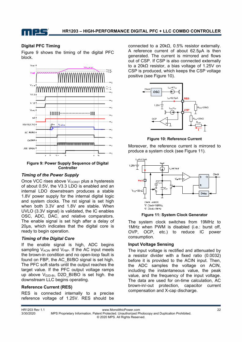
Digital PFC Timing
Figure 9 shows the timing of the digital PFC block.
Figure 9: Power Supply Sequence of Digital Controller
Timing of the Power Supply
Once VCC rises above VCCRST plus a hysteresis of about 0.5V, the V3.3 LDO is enabled and an internal LDO downstream produces a stable 1.8V power supply for the internal digital logic and system clocks. The rst signal is set high when both 3.3V and 1.8V are stable. When UVLO (3.3V signal) is validated, the IC enables OSC, ADC, DAC, and relative comparators. The enable signal is set high after a delay of 20µs, which indicates that the digital core is ready to begin operation.
Timing of the Digital Core
If the enable signal is high, ADC begins sampling VACIN and VFBP. If the AC input meets the brown-in condition and no open-loop fault is found on FBP, the AC_BI/BO signal is set high. The PFC soft starts until the output reaches the target value. If the PFC output voltage ramps up above VD2D-BI, D2D_BI/BO is set high. the downstream LLC begins operating.
Reference Current (RES)
RES is connected internally to a precise reference voltage of 1.25V. RES should be
connected to a 20kΩ, 0.5% resistor externally. A reference current of about 62.5µA is then generated. The current is mirrored and flows out of CSP. If CSP is also connected externally to a 20kΩ resistor, a bias voltage of 1.25V on CSP is produced, which keeps the CSP voltage positive (see Figure 10).
RCSP
1.25V
Iref=62.5μA
RRES=20kΩIbias=Iref
Rbias=20kΩ
Iosc=K*IrefClock
OCP
Figure 10: Reference Current
Moreover, the reference current is mirrored to produce a system clock (see Figure 11).
Figure 11: System Clock Generator
The system clock switches from 19MHz to 1MHz when PWM is disabled (i.e.: burst off, OVP, OCP, etc.) to reduce IC power consumption.
Input Voltage Sensing
The input voltage is rectified and attenuated by a resistor divider with a fixed ratio (0.0032) before it is provided to the ACIN input. Then, the ADC samples the voltage on ACIN, including the instantaneous value, the peak value, and the frequency of the input voltage. The data are used for on-time calculation, AC brown-in/-out protection, capacitor current compensation and X-cap discharge.
HR1203 – HIGH-PERFORMANCE DIGITAL PFC + LLC COMBO CONTROLLER
HR1203 Rev 1.1 www.MonolithicPower.com 23 3/30/2020 MPS Proprietary Information. Patent Protected. Unauthorized Photocopy and Duplication Prohibited. © 2020 MPS. All Rights Reserved.
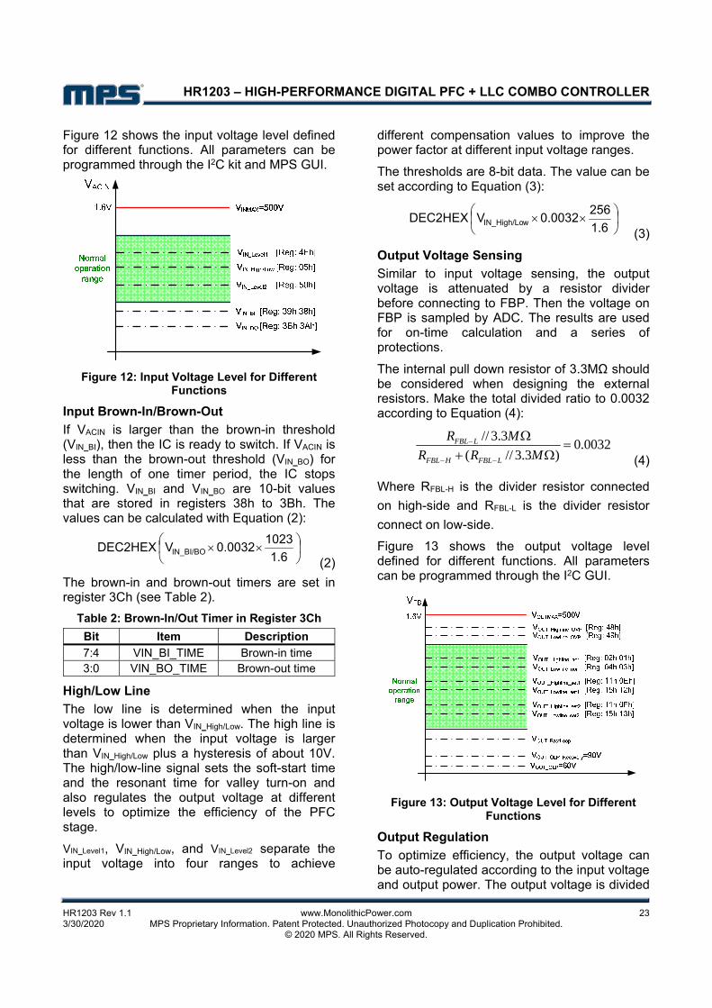
Figure 12 shows the input voltage level defined for different functions. All parameters can be programmed through the I2C kit and MPS GUI.
Figure 12: Input Voltage Level for Different Functions
Input Brown-In/Brown-Out
If VACIN is larger than the brown-in threshold (VIN_BI), then the IC is ready to switch. If VACIN is less than the brown-out threshold (VIN_BO) for the length of one timer period, the IC stops switching. VIN_BI and VIN_BO are 10-bit values that are stored in registers 38h to 3Bh. The values can be calculated with Equation (2):
6.1
10230032.0VDEC2HEX IN_BI/BO
(2)
The brown-in and brown-out timers are set in register 3Ch (see Table 2).
Table 2: Brown-In/Out Timer in Register 3Ch
Bit Item Description
7:4 VIN_BI_TIME Brown-in time 3:0 VIN_BO_TIME Brown-out time
High/Low Line
The low line is determined when the input voltage is lower than VIN_High/Low. The high line is determined when the input voltage is larger than VIN_High/Low plus a hysteresis of about 10V. The high/low-line signal sets the soft-start time and the resonant time for valley turn-on and also regulates the output voltage at different levels to optimize the efficiency of the PFC stage.
VIN_Level1, VIN_High/Low, and VIN_Level2 separate the input voltage into four ranges to achieve
different compensation values to improve the power factor at different input voltage ranges.
The thresholds are 8-bit data. The value can be set according to Equation (3):
6.1
2560032.0VDEC2HEX wIN_High/Lo
(3)
Output Voltage Sensing
Similar to input voltage sensing, the output voltage is attenuated by a resistor divider before connecting to FBP. Then the voltage on FBP is sampled by ADC. The results are used for on-time calculation and a series of protections.
The internal pull down resistor of 3.3MΩ should be considered when designing the external resistors. Make the total divided ratio to 0.0032 according to Equation (4):
// 3.30.0032
( // 3.3 )FBL L
FBL H FBL L
R M
R R M
(4)
Where RFBL-H is the divider resistor connected
on high-side and RFBL-L is the divider resistor
connect on low-side.
Figure 13 shows the output voltage level defined for different functions. All parameters can be programmed through the I2C GUI.
Figure 13: Output Voltage Level for Different Functions
Output Regulation
To optimize efficiency, the output voltage can be auto-regulated according to the input voltage and output power. The output voltage is divided

HR1203 – HIGH-PERFORMANCE DIGITAL PFC + LLC COMBO CONTROLLER
HR1203 Rev 1.1 www.MonolithicPower.com 24 3/30/2020 MPS Proprietary Information. Patent Protected. Unauthorized Photocopy and Duplication Prohibited. © 2020 MPS. All Rights Reserved.
into two ranges by VIN_High/Low and is divided into three ranges according to the output power level, which can be programmed by registers 06h to 09h. Therefore, the IC can auto-regulate six output voltages accordingly.
Output Fast OVP
VOUT_Highline_OVP and VOUT_Lowline_OVP are 7-bit values stored in register 48h and 49h. They are programmable through the I2C GUI (typically 430V). A 7-bit DAC converts VOUT_OVP to an analog signal and compares the result with the FBP voltage. If the output voltage is larger than VOUT_OVP, the PFC stops switching. Once the output voltage decreases to regulation voltage, the PFC resumes switching (see Figure 14).
Figure 14: OVP Circuit
A blanking time is inserted into OVP, keeping the IC immune to switching noise interference (see Figure 15). Both TOVP_T and TOVP_R are programmable in register 60h.
Figure 15: Output Fast OVP
Fast Loop
In a dynamic load event, the PFC output voltage decreases due to the low bandwidth of the voltage control loop, which causes the output voltage to fall out of regulation. Fast loop is activated when the output voltage is lower than VOUT_FastLoop. Then Ki and Kp of the digital PI are changed by X times the normal value depending on the GUI setting. In this way, the output voltage of the PFC is regulated faster in the dynamic load event.
Open Loop or IC Disable Condition
If the FBP voltage is less than VOUT_OLP (typically 60V), it is considered to be an open-loop or IC disable condition. The IC does not
work, and PWM switching is disabled. The IC restarts only when the FBP voltage is larger than VOUT_OLP_Recovery (typically 90V). The open loop is achieved by software and the value is fixed.
Peak Current Sensing
The PFC inductor current is sensed by RCSP and produces a negative voltage. The CSP pin sources out a precise current (Ibias) to produce a positive bias voltage on Rbias (see Figure 16).
The CSP voltage can be calculated with Equation (5):
t)(Vt)(Vt)(V CSCSP_BiasCSP
(5)
Figure 16: Current Sense Circuit in CSP
Overall, the CSP voltage is positive (see Figure 17). ADC samples VCSP_Bias (typically 1.25V) regularly.

HR1203 – HIGH-PERFORMANCE DIGITAL PFC + LLC COMBO CONTROLLER
HR1203 Rev 1.1 www.MonolithicPower.com 25 3/30/2020 MPS Proprietary Information. Patent Protected. Unauthorized Photocopy and Duplication Prohibited. © 2020 MPS. All Rights Reserved.
Figure 17: Voltage Waveform in CSP
Over-Current Protection (OCP)
If the CSP voltage is less than zero, over-current protection (OCP) is enabled. The PFC stops switching immediately, and OCP_trig is set high simultaneously. The digital core detects this status and disables PWM. OCP can be released by the OCP_release signal.
The OCP function is disabled by setting bit[3] of register 45h to logic low. The OCP behavior mode can be programmed by setting bit[2] to bit[0] of register 45h. It can be hiccup, latch, or auto-restart with a delay time. The default setting is hiccup. The delay time is set in register 46h.
A programmable LEB1 (TOCP_blanking) of about 200ns is implemented to avoid error sensing due to switching noise.
The OCP function can avoid over-stressing when the inductor is shorted or when the current is too large.
Figure 18 shows the operating waveforms of the OCP function.
Figure 18: OCP Operation Waveform
Over-Current Limit (OCL)
The inductor current achieves a cycle-by-cycle limit by setting the appropriate RCSP and VI-OCL. VI-OCL can be programmed in register 44h and can be converted to an analog signal by a 7-bit DAC. A programmable LEB1 (TOCL_blanking) of about 200ns is inserted to avoid switching noise if the digital core is turned on (similar to TOCP_blanking).

HR1203 – HIGH-PERFORMANCE DIGITAL PFC + LLC COMBO CONTROLLER
HR1203 Rev 1.1 www.MonolithicPower.com 26 3/30/2020 MPS Proprietary Information. Patent Protected. Unauthorized Photocopy and Duplication Prohibited. © 2020 MPS. All Rights Reserved.
Digital PFC Control Scheme
Figure 19 shows the flowchart of the digital PFC control scheme.
Figure 19: Flowchart of PFC Control Scheme
Digital Current Reference
The digital PI compensates for the voltage loop. Its output Vcomp(n) is sent to the multiplier for current reference calculation (see Figure 20).
s
KsK ip 2
in_avg
compin V
VV
Figure 20: Current Reference
The digital current reference can be calculated with Equation (6):
2
in_pk
compinref
(n))V5.0(
(n)V(n)V(n)I
(6)
On-Time Calculation
The on-time can be calculated with Equation (7):
so_ref
ino_refon T
V
(n)VV(n)T
(7)
Where Ts is the switching period, programmable in registers 1Eh to 22h.
Mode Decision
The HR1203 has three operation modes: continuous conduction mode (CCM), variable frequency discontinuous conduction mode (VF-DCM), and constant frequency discontinuous conduction mode (CF-DCM).
The peak value of the inductor current in CCM should satisfy Equation (8):
(n)I2(n)I refpk (8)
The peak value of the inductor current in VF-DCM should satisfy Equation (9):
s
s_maxrefpkref T
T(n)I2(n)I(n)I2 (9)
The peak value of the inductor current in CF-DCM should satisfy Equation (10):
s
s_maxrefpk T
T(n)I2(n)I (10)
Where Ts_max is the maximum switching period, programmable in registers from 23h to 27h.
1. CCM Operation:
When the converter operates in CCM, the off_cur_ref(n) is calculated and sent to the DAC. The output of the DAC is an analog signal (off_cur_ref(t)) and is compared with VCS(t). If VCS(t) is lower than off_cur_ref(t), the signal is set high. The PWM signal is set high accordingly (see Figure 21).
Figure 21: CCM Control Signals

HR1203 – HIGH-PERFORMANCE DIGITAL PFC + LLC COMBO CONTROLLER
HR1203 Rev 1.1 www.MonolithicPower.com 27 3/30/2020 MPS Proprietary Information. Patent Protected. Unauthorized Photocopy and Duplication Prohibited. © 2020 MPS. All Rights Reserved.
The off current reference at CCM can be calculated with Equation (11):
(n)I(n)I2f(n)off_cur_re pkref (11)
2. VF-DCM Operation
When the converter operates in VF-DCM, the off current reference is set to zero. In this case, the set signal represents the boundary of DCM (see Figure 22).
Figure 22: VF-DCM Control Signals
The new switching period is calculated with Equation (12):
sref
pks_new T
(n)I2
(n)I(n)T (12)
The delay time is calculated with Equation (13):
sref
pkss_newd T1
(n)I2
(n)IT(n)T(n)t
(13)
3. CF-DCM Operation
When the converter operates in CF-DCM, the off current reference is set to zero. In this mode, the switching frequency is limited to the minimum switching frequency (see Figure 23).
Figure 23: CF-DCM Control Signals
The PWM duty is modulated to achieve average current control. The new switching period is calculated with Equation (14):
s_max
pk
refs T
(n)I
(n)I2(n)T (14)
As ton changes minimally, the peak value of the inductor current can be seen as unchanged. See Equation (15):
(n)I(n)I pkpk (15)
The new turn-on time can be calculated with Equation (16):
(n)TV
(n)VV(n)t s
o_ref
ino_refon
(16)
The delay time is calculated with Equation (17):
s_maxpk
refss_maxd T
(n)I(n)I2
1)n(TT(n)t
(17)
Programmable Digital Filter
The HR1203 implements two programmable digital filters (Iref_filter and Td_filter) internally for noise immunity improvement. Register 3Dh is used to enable/disable each filter and program the bandwidth of the filters.
As shown in Figure 24, Iref_filter is implemented on the input of the PFC SET comparator. It helps reduce the current distortion and the audible noise in CCM operations.
Rbias
Rcsp
DACIref_off(n)
IL
Ibias
VCS
VCSP_Bias
SET
CSP
Filter
Figure 24: Iref_filter Circuit

HR1203 – HIGH-PERFORMANCE DIGITAL PFC + LLC COMBO CONTROLLER
HR1203 Rev 1.1 www.MonolithicPower.com 28 3/30/2020 MPS Proprietary Information. Patent Protected. Unauthorized Photocopy and Duplication Prohibited. © 2020 MPS. All Rights Reserved.
Figure 25: Td Control Signals
As shown in Figure 25, Td_filter is implemented on the calculation of the delay time. It helps reduce the current distortion in DCM operations. With Td_filter, the new delay time can be calculated with Equation (18):
1)(ntA1(n)tA(n)t d_newdd_new (18)
Where A is a coefficient related to the bandwidth of Td_filter. The bandwidth should be selected according to practical applications.
Soft Start (SS)
Once the AC input voltage is larger than VIN_BI, the Vin_ok signal pulls high, and the HR1203 initiates a soft-start sequence (see Figure 26).
Figure 26: Soft-Start Sequence
The output voltage rises from the rectified output voltage to the target value. When softstart_flag is set high, the soft-start sequence is completed. The soft-start time can be calculated with Equation (19):
slewrate
V
12)VV(T
adc_ref
bit_num
o_starto_targetss
(19)
Where Vo_target is the target value of the output voltage, Vo_start is the soft-start value of the
output voltage, bit_num is the ADC data bit (typically 12), Vadc_ref is the reference voltage of ADC (typically 1.6V).
The slew rate is different at high line and low line. The slew rate at high line is programmable in register 1Ch. the slew rate at the low line is programmable in register 1Dh.
Burst-Mode Operation
In light load, the IC is designed to always run in burst mode for better efficiency and lower no-load power consumption. Once the output load is lower than the threshold (e.g.: 3% rated load), the PFC enters burst mode. The threshold can be programmed in register 2Dh for high line and register 2Fh for low line. In burst mode, the switching duty is calculated based on the 3% rated load. The output is regulated to Vo_target with a 5V hysteresis. The PFC continues switching when the output voltage is below Vo_target - 5V. The PFC stops switching when the output voltage ramps up to Vo_target.
Generally, the HR1203 is designed to exit burst mode only at the peak point of the AC line to reduce current stress. Additionally, a threshold voltage that can be programmed in register 0Ah is selectable to prevent the bus voltage from dropping too low under transient conditions such as surge. If the bus voltage is lower than the threshold, the IC exits burst mode immediately without waiting for peak point detection.
Burst-mode operation is synchronized with the LLC_sync signal. If the LLC_sync signal is high, the PFC PWM switching is turned off. Once the output voltage is lower than Vo_target - 5V, the PFC is turned on again even if the LLC_sync signal is high. This status continues until the output voltage ramps up to Vo_target.
When the PFC recovers from burst mode, it operates in critical conduction mode (CRM) for the first five switching cycles.
Capacitor Current Compensation
Traditional PFC control schemes only regulate the inductor current to match the shape of the input voltage. However, the input capacitor current is not controlled, which may cause PF deterioration and an undesired delay. With a
HR1203 – HIGH-PERFORMANCE DIGITAL PFC + LLC COMBO CONTROLLER
HR1203 Rev 1.1 www.MonolithicPower.com 29 3/30/2020 MPS Proprietary Information. Patent Protected. Unauthorized Photocopy and Duplication Prohibited. © 2020 MPS. All Rights Reserved.
larger capacitor or a higher input voltage, the PF worsens.
To improve the PF, the HR1203 implements a patented method to compensate for PF deterioration. Relevant data are stored in registers 4Bh to 4Eh, corresponding to different input voltage levels. With this function, the PF is improved at all input voltage levels.
Frequency Jittering
To reduce EMI noise, the switching frequency is designed to be modulated by a triangular waveform with the frequency of fm. The switching frequency is modulated to the maximum value at the peak of the triangle and to the minimum value at the valley of the triangle. Figure 27 shows the algorithm modulating the switching frequency.
Figure 27: Frequency Jittering
The parameters of fsw_max, fsw_min, and fm can be programmed by the I2C GUI for the best EMI performance.
PART 4: LLC CONTROLLER
Oscillator (FSET)
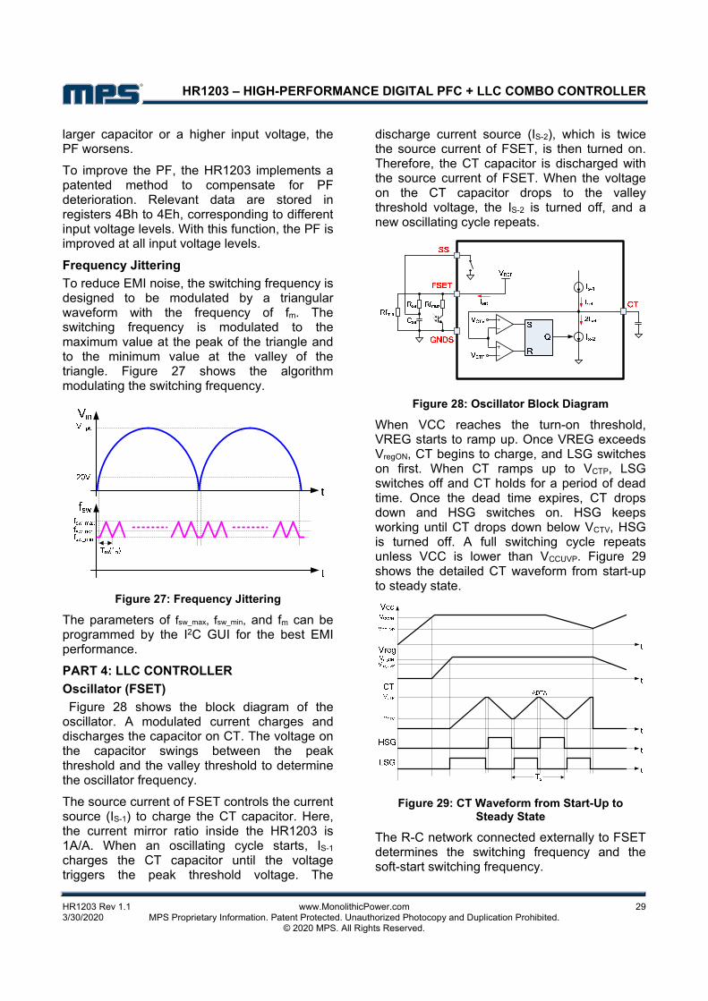
Figure 28 shows the block diagram of the oscillator. A modulated current charges and discharges the capacitor on CT. The voltage on the capacitor swings between the peak threshold and the valley threshold to determine the oscillator frequency.
The source current of FSET controls the current source (IS-1) to charge the CT capacitor. Here, the current mirror ratio inside the HR1203 is 1A/A. When an oscillating cycle starts, IS-1 charges the CT capacitor until the voltage triggers the peak threshold voltage. The
discharge current source (IS-2), which is twice the source current of FSET, is then turned on. Therefore, the CT capacitor is discharged with the source current of FSET. When the voltage on the CT capacitor drops to the valley threshold voltage, the IS-2 is turned off, and a new oscillating cycle repeats.
Figure 28: Oscillator Block Diagram
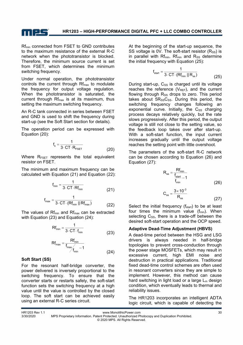
When VCC reaches the turn-on threshold, VREG starts to ramp up. Once VREG exceeds VregON, CT begins to charge, and LSG switches on first. When CT ramps up to VCTP, LSG switches off and CT holds for a period of dead time. Once the dead time expires, CT drops down and HSG switches on. HSG keeps working until CT drops down below VCTV, HSG is turned off. A full switching cycle repeats unless VCC is lower than VCCUVP. Figure 29 shows the detailed CT waveform from start-up to steady state.
Figure 29: CT Waveform from Start-Up to Steady State
The R-C network connected externally to FSET determines the switching frequency and the soft-start switching frequency.
HR1203 – HIGH-PERFORMANCE DIGITAL PFC + LLC COMBO CONTROLLER
HR1203 Rev 1.1 www.MonolithicPower.com 30 3/30/2020 MPS Proprietary Information. Patent Protected. Unauthorized Photocopy and Duplication Prohibited. © 2020 MPS. All Rights Reserved.
Rfmin connected from FSET to GND contributes to the maximum resistance of the external R-C network when the phototransistor is blocked. Therefore, the minimum source current is set from FSET, which determines the minimum switching frequency.
Under normal operation, the phototransistor controls the current through Rfmax to modulate the frequency for output voltage regulation. When the phototransistor is saturated, the current through Rfmax is at its maximum, thus setting the maximum switching frequency.
An R-C tank connected in series between FSET and GND is used to shift the frequency during start-up (see the Soft Start section for details).
The operation period can be expressed with Equation (20):
FSETs RCT3
1f
(20)
Where RFSET represents the total equivalent resistor on FSET.
The minimum and maximum frequency can be calculated with Equation (21) and Equation (22):
minmin RfCT3
1f
(21)
)Rf||Rf(CT3
1f
maxminmax
(22)
The values of Rfmin and Rfmax can be extracted with Equation (23) and Equation (24):
minmin fCT3
1Rf
(23)
1f
fRf
Rf
min
max
minmax
(24)
Soft Start (SS)
For the resonant half-bridge converter, the power delivered is inversely proportional to the switching frequency. To ensure that the converter starts or restarts safely, the soft-start function sets the switching frequency at a high value until the value is controlled by the closed loop. The soft start can be achieved easily using an external R-C series circuit.
At the beginning of the start-up sequence, the SS voltage is 0V. The soft-start resistor (RSS) is in parallel with Rfmin. Rfmin and RSS determine the initial frequency with Equation (25):
)R||Rf(CT3
1f
ssminstart
(25)
During start-up, CSS is charged until its voltage reaches the reference (VREF), and the current flowing through RSS drops to zero. This period takes about 5RSSCSS. During this period, the switching frequency changes following an exponential curve. Initially, the CSS charging process decays relatively quickly, but the rate slows progressively. After this period, the output voltage is still not close to the setting value, so the feedback loop takes over after start-up. With a soft-start function, the input current increases gradually until the output voltage reaches the setting point with little overshoot.
The parameters of the soft-start R-C network can be chosen according to Equation (26) and Equation (27):
1
ffRf
R
min
start
minss
(26)
ss
-3
ss R103
C
(27)
Select the initial frequency (fstart) to be at least four times the minimum value (fmin). When selecting CSS, there is a trade-off between the desired soft-start operation and the OCP speed.
Adaptive Dead-Time Adjustment (HBVS)
A dead-time period between the HSG and LSG drivers is always needed in half-bridge topologies to prevent cross-conduction through the power stage MOSFETs, which may result in excessive current, high EMI noise and destruction in practical applications. Traditional fixed dead-time control schemes are often used in resonant converters since they are simple to implement. However, this method can cause hard switching in light load or a large Lm design condition, which eventually leads to thermal and reliability issues.
The HR1203 incorporates an intelligent ADTA logic circuit, which is capable of detecting the
HR1203 – HIGH-PERFORMANCE DIGITAL PFC + LLC COMBO CONTROLLER
HR1203 Rev 1.1 www.MonolithicPower.com 31 3/30/2020 MPS Proprietary Information. Patent Protected. Unauthorized Photocopy and Duplication Prohibited. © 2020 MPS. All Rights Reserved.
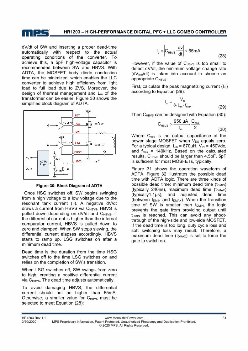
dV/dt of SW and inserting a proper dead-time automatically with respect to the actual operating conditions of the converter. To achieve this, a 5pF high-voltage capacitor is recommended between SW and HBVS. With ADTA, the MOSFET body diode conduction time can be minimized, which enables the LLC converter to achieve high efficiency from light load to full load due to ZVS. Moreover, the design of thermal management and Lm of the transformer can be easier. Figure 30 shows the simplified block diagram of ADTA.
Figure 30: Block Diagram of ADTA
Once HSG switches off, SW begins swinging from a high voltage to a low voltage due to the resonant tank current (Ir). A negative dV/dt draws a current from HBVS via CHBVS. HBVS is pulled down depending on dV/dt and CHBVS. If the differential current is higher than the internal comparator current, HBVS is pulled down to zero and clamped. When SW stops slewing, the differential current elapses accordingly. HBVS starts to ramp up. LSG switches on after a minimum dead time.
Dead time is the duration from the time HSG switches off to the time LSG switches on and relies on the completion of SW’s transition.
When LSG switches off, SW swings from zero to high, creating a positive differential current via CHBVS. The dead time adjusts automatically.
To avoid damaging HBVS, the differential current should not be higher than 65mA. Otherwise, a smaller value for CHBVS must be selected to meet Equation (28):
mA65
dt
dv·Ci HBVSd <=
(28)
However, if the value of CHBVS is too small to detect dV/dt, the minimum voltage change rate (dVmin/dt) is taken into account to choose an appropriate CHBVS.
First, calculate the peak magnetizing current (Im)
according to Equation (29):
maxm
inm fL8
VI
(29)
Then CHBVS can be designed with Equation (30):
2C
IμA950
C oss
mHBVS
(30)
Where Coss is the output capacitance of the power stage MOSFET when VDS equals zero. For a typical design, Lm = 870µH, VIN = 450Vdc, and fmax = 140kHz. Based on the calculated results, CHBVS should be larger than 4.5pF. 5pF is sufficient for most MOSFETs, typically.
Figure 31 shows the operation waveform of ADTA. Figure 32 illustrates the possible dead time with ADTA logic. There are three kinds of possible dead time: minimum dead time (tDMIN) (typically 240ns), maximum dead time (tDMAX) (typically1.1µs), and adjusted dead time (between tDMIN and tDMAX). When the transition time of SW is smaller than tDMIN, the logic prevents the gate from providing output until tDMIN is reached. This can avoid any shoot-through of the high-side and low-side MOSFET. If the dead time is too long, duty cycle loss and soft switching loss may result. Therefore, a maximum dead time (tDMAX) is set to force the gate to switch on.

HR1203 – HIGH-PERFORMANCE DIGITAL PFC + LLC COMBO CONTROLLER
HR1203 Rev 1.1 www.MonolithicPower.com 32 3/30/2020 MPS Proprietary Information. Patent Protected. Unauthorized Photocopy and Duplication Prohibited. © 2020 MPS. All Rights Reserved.
Figure 31: Operation Waveform of ADTA
Figure 32: Dead Time in ADTA
If HBVS is shorted to GND, LLC stops switching. If HBVS is floating, the internal circuit cannot detect the differential current in HBVS, and the fixed dead time (300ns) takes effect.
Capacitive Mode Protection (CMP, CSHB)
In fault conditions such as overload or short-circuit condition, the converter may run into the capacitive region. In capacitive mode, the voltage applied to the resonant tank lags off the current. The body diode of one of the MOSFETs switches on. To avoid device damage, the switching of the other MOSFET should be blocked. The functional block diagram of CMP is shown in Figure 33.
Figure 33: CMP and OCP Block Diagram
Figure 34 shows the operating principle of capacitive mode protection. CSPOS and CSNEG stand for the current polarity, which is generated by comparing the voltage of CS with an internal +80mV and -80mV voltage reference.
Figure 34: Operating Principle of CMP
At t0, the low-side gate driver switches off for the first time. CSNEG is high, which means the current is at the correct polarity, so the converter is operating in inductive mode. The capacitive mode protection circuit is not active.
At t1, the high-side gate driver switches off for the first time. CSPOS is high, so the current is at the correct polarity, and the converter operates in inductive mode. The capacitive mode protection circuit is still not active.
At t2, the low-side gate driver turns off for a second time. CSNEG is zero and CSPOS is

HR1203 – HIGH-PERFORMANCE DIGITAL PFC + LLC COMBO CONTROLLER
HR1203 Rev 1.1 www.MonolithicPower.com 33 3/30/2020 MPS Proprietary Information. Patent Protected. Unauthorized Photocopy and Duplication Prohibited. © 2020 MPS. All Rights Reserved.
high, which means the converter is operating in capacitive mode. The body diode of the low-side MOSFET takes over the current after the low-side MOSFET turns off. SW does not turn high, so HBVS cannot catch the dV/dt until the current returns to the correct polarity. The dead time remains high, and VCO is held. Another MOSFET does not switch on. So, capacitive switching is prevented effectively.
At t3, the current returns to the correct polarity, then another MOSFET is turned on due to dV/dt being captured.
If the correct current polarity cannot be detected from t2 to t4, or the current is very small and is not capable of pulling SW up or down, eventually another MOSFET is forced to switch on when the timer for CMP (50µs) expires (see the dashed lines in Figure 34).
The VSS control signal controls the soft start. When capacitive mode operation is detected, VSS is high. An internal MOSFET is turned on to pull the voltage of CSS low. Therefore, the switching frequency increases quickly to limit the power delivered to the output. VSS is reset when the first gate driver is turned off (after CMP). The switching frequency decreases smoothly until the control loop takes over.
Over-Current Regulation and Over-Current Protection (CSHB, TIMER)
The HR1203 provides two levels of over-current protection (see Figure 35).
Figure 35: OCR Timing Sequence
1. Over-current regulation:
The first level of protection occurs when the voltage on CSHB exceeds VCS-OCR (0.77V). When this occurs, the transistor connected
internally between SS and GND is turned on for at least 10µs, which causes the CSS voltage to drop down, resulting in a sharp increase in the oscillator frequency. Hence, the energy transferred to the output is reduced. An internal 140µA current source is turned on to charge CTIMER and raises the voltage of TIMER. If the CSHB voltage drops below VCS-OCR (10mV hysteresis) before the TIMER voltage reaches Vth1 (1.97V), the discharging of CSS and the charging of CTIMER stop. Then the converter resumes normal operation.
tOC represents the time for the CTIMER voltage to rise from 0V to Vth1. This is actually a delay time for over-current regulation. There is no simple relationship between tOC and CTIMER. CTIMER is selected based on experimental results.
If the CSHB voltage remains larger than VCS-OCR after the TIMER voltage reaches Vth1, CSS is discharged completely. Simultaneously, the internal 140µA current source continues charging CTIMER until the TIMER voltage reaches Vth2 (3.45V). At this time, the IC turns off all gate driver outputs.
The period for the TIMER voltage to rise from Vth1 to Vth2 can be calculated approximately by using Equation (31):
TIMER4
OP C10t (31)
The above status remains until VTIMER drops to Vth3 (0.29V) as CTIMER is discharged slowly by RTIMER. The IC then restarts. The time period can be calculated using Equation (32):
TIMERTIMERTIMERTIMERth3
th2OFF CR5.2CR
VV
lnt (32)
The OCR limits the energy transferred from the primary to the secondary winding during overload or short-circuit period. However, excessive power consumption due to high continuous currents can damage the secondary-side windings and rectifiers. By incorporating the TIMER function, the IC provides additional protection to reduce the average power consumption. When OCR is triggered, the converter enters a hiccup-like protection mode that operates intermittently. Figure 35 shows the timing procedure.
HR1203 – HIGH-PERFORMANCE DIGITAL PFC + LLC COMBO CONTROLLER
HR1203 Rev 1.1 www.MonolithicPower.com 34 3/30/2020 MPS Proprietary Information. Patent Protected. Unauthorized Photocopy and Duplication Prohibited. © 2020 MPS. All Rights Reserved.
Over-current protection:
The second level of protection is triggered when VCS > VCS-OCP (1.48V). Normally, this condition occurs when the CSHB voltage continues rising during short-circuit period. Once VCS rises to VCS-OCP, the IC does not stop switching immediately until VSS < VSS-OCP, and CSS is discharged by an internal transistor continuously. If VCS remains above VCS-OCP until VSS drops below VSS-OCP, the IC shuts down. CTIMER is charged by an internal 140µA current source until the TIMER voltage reaches Vth2. The IC resumes operation if the TIMER voltage falls below Vth3.
The OCP provides a high-speed over-current limitation. The IC works in auto-recovery mode when OCP triggers.
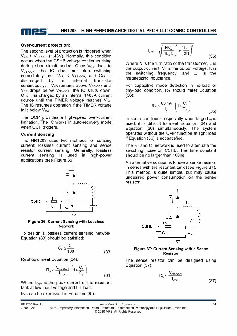
Current Sensing
The HR1203 uses two methods for sensing current: lossless current sensing and sense resistor current sensing. Generally, lossless current sensing is used in high-power applications (see Figure 36).
Figure 36: Current Sensing with Lossless Network
To design a lossless current sensing network, Equation (33) should be satisfied:
100C
C rS
(33)
RS should meet Equation (34):
S
r
Crpk
OCR-CSS C
C1
IV
R (34)
Where ICrpk is the peak current of the resonant tank at low input voltage and full load.
ICrpk can be expressed in Equation (35):
2o
2
sm
oCrpk 2N
I
f4L
NVI
π
(35)
Where N is the turn ratio of the transformer, lo is the output current, Vo is the output voltage, fs is the switching frequency, and Lm is the magnetizing inductance.
For capacitive mode detection in no-load or tiny-load condition, RS should meet Equation (36):
S
r
mS C
C1
ImV08
R (36)
In some conditions, especially when large Lm is used, it is difficult to meet Equation (34) and Equation (36) simultaneously. The system operates without the CMP function at light load if Equation (36) is not satisfied.
The R1 and C1 network is used to attenuate the switching noise on CSHB. The time constant should be no larger than 100ns.
An alternative solution is to use a sense resistor in series with the resonant tank (see Figure 37). This method is quite simple, but may cause undesired power consumption on the sense resistor.
Figure 37: Current Sensing with a Sense Resistor
The sense resistor can be designed using Equation (37):
Crpk
OCR-CSS I
VR
(37)

HR1203 – HIGH-PERFORMANCE DIGITAL PFC + LLC COMBO CONTROLLER
HR1203 Rev 1.1 www.MonolithicPower.com 35 3/30/2020 MPS Proprietary Information. Patent Protected. Unauthorized Photocopy and Duplication Prohibited. © 2020 MPS. All Rights Reserved.
LLC Brown-In/Brown-Out (D2D_BI/BO)
The LLC controller stops when the D2D_BI/BO signal is low and recovers once the D2D_BI/BO signal goes high.
Burst-Mode Operation (BURST)
Under light-load or no-load condition, the resonant half-bridge switching frequency is limited by the system maximum frequency. To control the output voltage and limit the power consumption, the HR1203 enables the converter to operate in burst mode to reduce the average switching frequency, reducing the average residual magnetizing current and related power losses.
Figure 38 shows a typical circuit connecting BURST to the feedback signal. RBURST and CBURST must be optimized to adjust the number of switching cycles during the burst-on period, which can reduce no-load power consumption. Rfmax can determine the maximum switching frequency, which is needed for the IC to operate in burst mode and determines the level of output load needed to run in burst mode.
Vth
IsetVCO
VREFCT
Css
Burst control
RfminRfmax
RBURST
Rss
CBURST
Figure 38: Burst-Mode Operation Set-Up
Figure 39 illustrates the burst-mode operation waveforms. When the output load decreases, the BURST voltage also decreases. If the BURST voltage drops below Vth (1.23V), the HR1203 stops switching both the HSG and LSG and connects CT to GNDS internally. Meanwhile, the SYN signal is set high. It is used to synchronize the burst of PFC and LLC. Once the voltage on BURST exceeds Vth by a hysteresis of 40mV, the HR1203 resumes normal operation and the SYN signal is set low. During burst-mode operation, VREG normally
holds above VregUVP, and the soft-start function is not activated.
Figure 39: Burst-Mode Operation
Latch Protection (SO)
If the SO voltage exceeds the threshold (VSO-
Latch) (3.42V), the IC latches off. This status can only be released when VCC drops below VCCRST. This function can be used for OVP or OTP.
Start-Up Failure Protection (SFP, SO)
The HR1203 provides a one-shot start-up failure protection by sampling the SO voltage. Figure 40 shows the detailed SFP timing.
Figure 40: SFP Timing
During start-up, the TIMER capacitor starts charging up via an internal 25µA current source. If the SO voltage is less than VSO-SFP (1.96V) when the TIMER voltage rises up to Vth1, then the IC treats this as a fault condition. The HR1203 begins discharging the SS capacitor, and TIMER continues ramping up irreversibly.

HR1203 – HIGH-PERFORMANCE DIGITAL PFC + LLC COMBO CONTROLLER
HR1203 Rev 1.1 www.MonolithicPower.com 36 3/30/2020 MPS Proprietary Information. Patent Protected. Unauthorized Photocopy and Duplication Prohibited. © 2020 MPS. All Rights Reserved.
Once the TIMER voltage reaches Vth2, the HR1203 stops charging TIMER, and both PFC and LLC stop switching. Since there is a resistor in parallel with the TIMER capacitor, the TIMER voltage is pulled down gradually. The IC attempts another start-up sequence until the TIMER voltage falls below Vth3.
Connect SO to the resistor divider from V3.3 if the SO function is not needed.
High-Side Gate Driver (HSG)
The external BST capacitor provides energy to the high-side gate driver. An integrated bootstrap diode charges this capacitor through VCC. This diode simplifies the external driving circuit for the high-side switch, allowing the BST capacitor to be charged when the low-side MOSFET is on.
Considering the BST capacitor charging time, to provide enough gate driver energy, a BST capacitor of 100nF to 1μF is recommended (see Figure 41).
Figure 41: High-Side Gate Driver
Low-Side Gate Driver (LSG)
LSG provides the gate driver signal for the low-side MOSFET. The Maximum Absolute Ratings table on page 5 shows that the maximum LSG voltage is 14V. Under certain conditions, such as the surge rating being too high, a large voltage spike may occur on the LSG due to oscillations from the long gate-driver wire, the MOSFET parasitic capacitance, and the small gate-driver resistor. The voltage spike may cause damage to the LSG. Although there is suppression internally in the chip, it is better to add a 13V Zener diode close to LSG and GND to prevent damage to the chip pins (see Figure 42).
Figure 42: Low-Side Gate Driver

HR1203 – HIGH-PERFORMANCE DIGITAL PFC + LLC COMBO CONTROLLER
HR1203 Rev 1.1 www.MonolithicPower.com 37 3/30/2020 MPS Proprietary Information. Patent Protected. Unauthorized Photocopy and Duplication Prohibited. © 2020 MPS. All Rights Reserved.
PROTECTION SUMMARY Pin Symbol Description Affected Action
VCC VCCUVP Under-voltage protection for VCC System Disable
VCC VCCSCP Short-circuit protection for VCC System Disable and limit IHV
VREG VregUVP Under-voltage protection for VREG System Disable and limit Ich
SO VSO-Latch Latch protection System Shutdown and latch
SO VSO-SFP Start-up failure protection System Restart with timer out
OTP Over-temperature protection System Disable
ACIN Brown-out Line input under-voltage protection System Suspend switching
CSP OCP_PFC Current limit of PFC PFC Program with restart or latch off
FBP OVP_PFC Over voltage of PFC PFC Suspend switching
FBP OLP_PFC Open-loop protection System Restart with recovery
FBP UVP_PFC Under-voltage protection for PFC output HBC Suspend switching
LLC brown-in/-out LLC stage under-voltage protection HBC Suspend switching
CSHB OCR_HBC Over-current regulation of HBC HBC Restart with timer out
CSHB OCP_HBC Over-current protection of HBC HBC Shutdown, restart with timer out
CSHB CMR Capacitive mode regulation HBC Increasing switching frequency
CSHB ADT Adaptive dead time HBC Prevent hard switching

HR1203 – HIGH-PERFORMANCE DIGITAL PFC + LLC COMBO CONTROLLER
HR1203 Rev 1.1 www.MonolithicPower.com 38 3/30/2020 MPS Proprietary Information. Patent Protected. Unauthorized Photocopy and Duplication Prohibited. © 2020 MPS. All Rights Reserved.
TYPICAL APPLICATION CIRCUIT
294k
36k
Figure 41: Typical Application Circuit
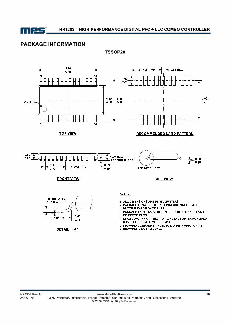
HR1203 – HIGH-PERFORMANCE DIGITAL PFC + LLC COMBO CONTROLLER
HR1203 Rev 1.1 www.MonolithicPower.com 39 3/30/2020 MPS Proprietary Information. Patent Protected. Unauthorized Photocopy and Duplication Prohibited. © 2020 MPS. All Rights Reserved.
PACKAGE INFORMATION
TSSOP28

HR1203 – HIGH-PERFORMANCE DIGITAL PFC + LLC COMBO CONTROLLER
HR1203 Rev 1.1 www.MonolithicPower.com 40 3/30/2020 MPS Proprietary Information. Patent Protected. Unauthorized Photocopy and Duplication Prohibited. © 2020 MPS. All Rights Reserved.
PACKAGE INFORMATION (continued) SOIC-28

HR1203 – HIGH-PERFORMANCE DIGITAL PFC + LLC COMBO CONTROLLER
HR1203 Rev 1.1 www.MonolithicPower.com 41 3/30/2020 MPS Proprietary Information. Patent Protected. Unauthorized Photocopy and Duplication Prohibited. © 2020 MPS. All Rights Reserved.
APPENDIX A: I2C COMMANDS AND REGISTERS VOUT_CMD_H (02/01h, 10 bits)
Sets the normal value of the output voltage target at high line. The default setting for the -0001 version is 1100011110.
Command VOUT_CMD_H
Bit 15 14 13 12 11 10 9 8 7 6 5 4 3 2 1 0
Access r r r r r r r/w r/w r/w r/w r/w r/w r/w r/w r/w r/w
VOUT_CMD_L (04/03h, 10 bits)
Sets the normal value of the output voltage target at low line. The default setting for the -0001 version is 1100011110.
Command VOUT_CMD_L Bit 15 14 13 12 11 10 9 8 7 6 5 4 3 2 1 0 Access r r r r r r r/w r/w r/w r/w r/w r/w r/w r/w r/w r/w
VIN_HL_LINE (05h, 8 bits)
Sets the threshold of the high line and low line. The default setting for the -0001 version is 01110001.
Command VIN_HL_LINE Bit 7 6 5 4 3 2 1 0Access r/w r/w r/w r/w r/w r/w r/w r/w
AUTO_VOUT_VCOMP1 (07/06h, 14 bits)
Sets the Load Level 1 of the auto-output voltage. The default setting for the -0001 version is 00011111111100.
Command AUTO_VOUT_VCOMP1 Bit 15 14 13 12 11 10 9 8 7 6 5 4 3 2 1 0 Access r r r/w r/w r/w r/w r/w r/w r/w r/w r/w r/w r/w r/w r/w r/w
AUTO_VOUT_VCOMP2 (09/08h, 14 bits)
Sets the Load Level 2 of the auto-output voltage. The default setting for the -0001 version is 00001100110010.
Command AUTO_VOUT_VCOMP2
Bit 15 14 13 12 11 10 9 8 7 6 5 4 3 2 1 0
Access r r r/w r/w r/w r/w r/w r/w r/w r/w r/w r/w r/w r/w r/w r/w
BURST_VOUT_LIMIT (0Ah, 5 bits)
Sets the threshold voltage of exiting burst mode. The default setting for the -0001 version is 10111.
Command BURST_VOUT_LIMIT
Bit 7 6 5 4 3 2 1 0
Access r r r r/w r/w r/w r/w r/w
AUTO_VOUT_CMPHYS (0D/0Ch, 14 bits)
Sets the load hysteresis of the auto-output voltage. The default setting for the -0001 version is 00000011110101.
Command AUTO_VOUT_CMPHYS
Bit 15 14 13 12 11 10 9 8 7 6 5 4 3 2 1 0
Access r r r/w r/w r/w r/w r/w r/w r/w r/w r/w r/w r/w r/w r/w r/w

HR1203 – HIGH-PERFORMANCE DIGITAL PFC + LLC COMBO CONTROLLER
HR1203 Rev 1.1 www.MonolithicPower.com 42 3/30/2020 MPS Proprietary Information. Patent Protected. Unauthorized Photocopy and Duplication Prohibited. © 2020 MPS. All Rights Reserved.
AUTO_VOUTH_CMD1_L (0Eh, 8 bits)
Sets the low byte of the output voltage level one at high line. The default setting for the -0001 version is 00011110.
Command AUTO_VOUTH_CMD1_L
Bit 7 6 5 4 3 2 1 0
Access r/w r/w r/w r/w r/w r/w r/w r/w
AUTO_VOUTH_CMD2_L (0Fh, 8 bits)
Sets the low byte of the output voltage level two at high line. The default setting for the -0001 version is 00011110.
Command AUTO_VOUTH_CMD2_L
Bit 7 6 5 4 3 2 1 0
Access r/w r/w r/w r/w r/w r/w r/w r/w
AUTO_VOUTH_CMD_H (11h, 4 bits)
Sets the high byte of the output voltage at high line. The default setting for the -0001 version is 1111.
Bit Item Description
3:2 AUTO_VOUTH_CMD2_H High bits of output voltage level two at high line.
1:0 AUTO_VOUTH_CMD1_H High bits of output voltage level one at high line.
Command AUTO_VOUTH_CMD_H
Bit 7 6 5 4 3 2 1 0
Access r r r r r/w r/w r/w r/w
AUTO_VOUTL_CMD1_L (12h, 8 bits)
Sets the low byte of the output voltage level one at low line. The default setting for the -0001 version is 00011110.
Command AUTO_VOUTL_CMD1_L
Bit 7 6 5 4 3 2 1 0
Access r/w r/w r/w r/w r/w r/w r/w r/w
AUTO_VOUTL_CMD2_L (13h, 8 bits)
Sets the low byte of the output voltage level two at low line. The default setting for the -0001 version is 00011110.
Command AUTO_VOUTL_CMD2_L
Bit 7 6 5 4 3 2 1 0
Access r/w r/w r/w r/w r/w r/w r/w r/w
AUTO_VOUTL_CMD_H (15h, 4 bits)
Sets the high byte of the output voltage at low line. The default setting for the -0001 version is 1111.
Bit Item Description
3:2 AUTO_VOUTL_CMD2_H High bits of output voltage level two at low line.
1:0 AUTO_VOUTL_CMD1_H High bits of output voltage level one at low line.
Command AUTO_VOUTL_CMD_H
Bit 7 6 5 4 3 2 1 0
Access r r r r r/w r/w r/w r/w
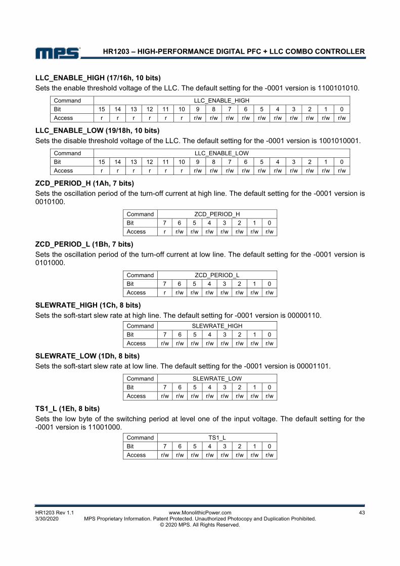
HR1203 – HIGH-PERFORMANCE DIGITAL PFC + LLC COMBO CONTROLLER
HR1203 Rev 1.1 www.MonolithicPower.com 43 3/30/2020 MPS Proprietary Information. Patent Protected. Unauthorized Photocopy and Duplication Prohibited. © 2020 MPS. All Rights Reserved.
LLC_ENABLE_HIGH (17/16h, 10 bits)
Sets the enable threshold voltage of the LLC. The default setting for the -0001 version is 1100101010.
Command LLC_ENABLE_HIGH
Bit 15 14 13 12 11 10 9 8 7 6 5 4 3 2 1 0
Access r r r r r r r/w r/w r/w r/w r/w r/w r/w r/w r/w r/w
LLC_ENABLE_LOW (19/18h, 10 bits)
Sets the disable threshold voltage of the LLC. The default setting for the -0001 version is 1001010001.
Command LLC_ENABLE_LOW
Bit 15 14 13 12 11 10 9 8 7 6 5 4 3 2 1 0
Access r r r r r r r/w r/w r/w r/w r/w r/w r/w r/w r/w r/w
ZCD_PERIOD_H (1Ah, 7 bits)
Sets the oscillation period of the turn-off current at high line. The default setting for the -0001 version is 0010100.
Command ZCD_PERIOD_H
Bit 7 6 5 4 3 2 1 0
Access r r/w r/w r/w r/w r/w r/w r/w
ZCD_PERIOD_L (1Bh, 7 bits)
Sets the oscillation period of the turn-off current at low line. The default setting for the -0001 version is 0101000.
Command ZCD_PERIOD_L
Bit 7 6 5 4 3 2 1 0
Access r r/w r/w r/w r/w r/w r/w r/w
SLEWRATE_HIGH (1Ch, 8 bits)
Sets the soft-start slew rate at high line. The default setting for -0001 version is 00000110.
Command SLEWRATE_HIGH
Bit 7 6 5 4 3 2 1 0
Access r/w r/w r/w r/w r/w r/w r/w r/w
SLEWRATE_LOW (1Dh, 8 bits)
Sets the soft-start slew rate at low line. The default setting for the -0001 version is 00001101.
Command SLEWRATE_LOW
Bit 7 6 5 4 3 2 1 0
Access r/w r/w r/w r/w r/w r/w r/w r/w
TS1_L (1Eh, 8 bits)
Sets the low byte of the switching period at level one of the input voltage. The default setting for the -0001 version is 11001000.
Command TS1_L
Bit 7 6 5 4 3 2 1 0
Access r/w r/w r/w r/w r/w r/w r/w r/w
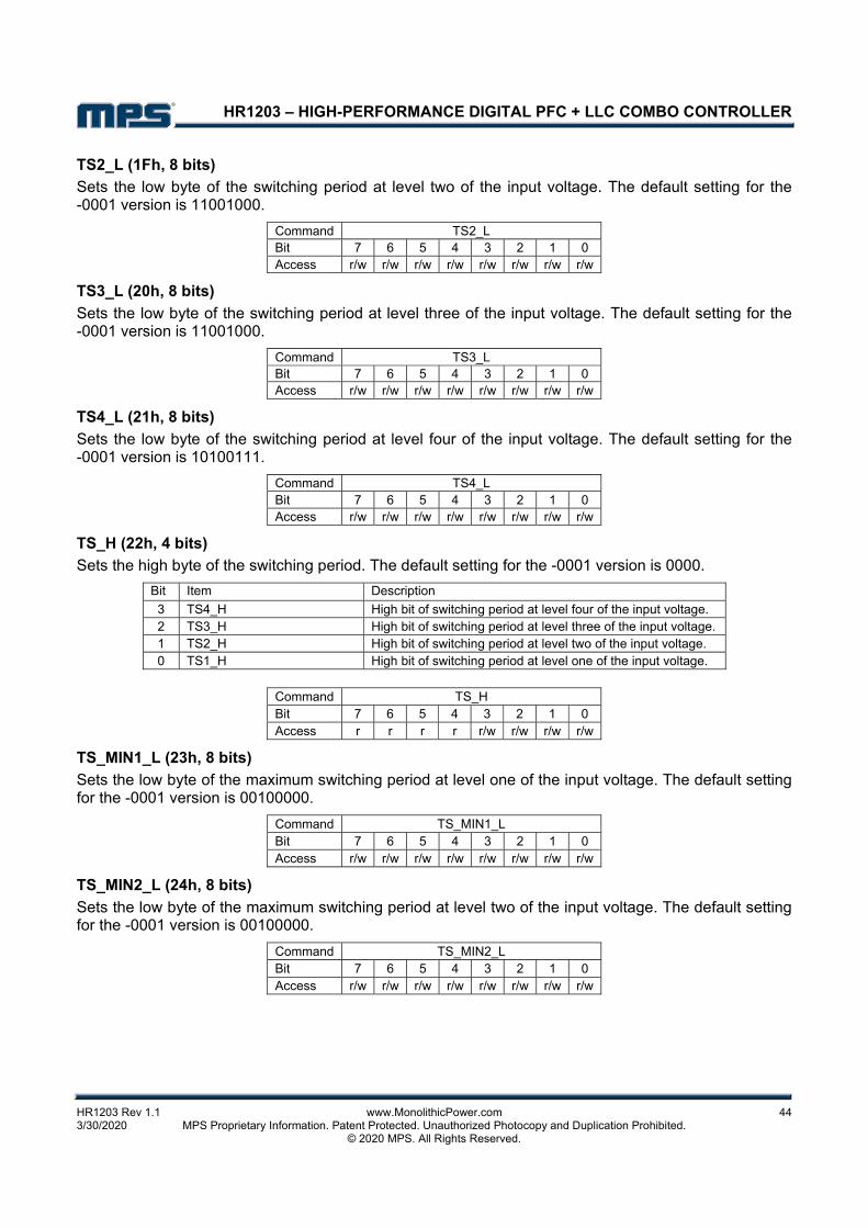
HR1203 – HIGH-PERFORMANCE DIGITAL PFC + LLC COMBO CONTROLLER
HR1203 Rev 1.1 www.MonolithicPower.com 44 3/30/2020 MPS Proprietary Information. Patent Protected. Unauthorized Photocopy and Duplication Prohibited. © 2020 MPS. All Rights Reserved.
TS2_L (1Fh, 8 bits)
Sets the low byte of the switching period at level two of the input voltage. The default setting for the -0001 version is 11001000.
Command TS2_L Bit 7 6 5 4 3 2 1 0Access r/w r/w r/w r/w r/w r/w r/w r/w
TS3_L (20h, 8 bits)
Sets the low byte of the switching period at level three of the input voltage. The default setting for the -0001 version is 11001000.
Command TS3_L Bit 7 6 5 4 3 2 1 0Access r/w r/w r/w r/w r/w r/w r/w r/w
TS4_L (21h, 8 bits)
Sets the low byte of the switching period at level four of the input voltage. The default setting for the -0001 version is 10100111.
Command TS4_L Bit 7 6 5 4 3 2 1 0Access r/w r/w r/w r/w r/w r/w r/w r/w
TS_H (22h, 4 bits)
Sets the high byte of the switching period. The default setting for the -0001 version is 0000.
Bit Item Description
3 TS4_H High bit of switching period at level four of the input voltage. 2 TS3_H High bit of switching period at level three of the input voltage. 1 TS2_H High bit of switching period at level two of the input voltage. 0 TS1_H High bit of switching period at level one of the input voltage.
Command TS_H Bit 7 6 5 4 3 2 1 0Access r r r r r/w r/w r/w r/w
TS_MIN1_L (23h, 8 bits)
Sets the low byte of the maximum switching period at level one of the input voltage. The default setting for the -0001 version is 00100000.
Command TS_MIN1_L Bit 7 6 5 4 3 2 1 0Access r/w r/w r/w r/w r/w r/w r/w r/w
TS_MIN2_L (24h, 8 bits)
Sets the low byte of the maximum switching period at level two of the input voltage. The default setting for the -0001 version is 00100000.
Command TS_MIN2_L Bit 7 6 5 4 3 2 1 0Access r/w r/w r/w r/w r/w r/w r/w r/w

HR1203 – HIGH-PERFORMANCE DIGITAL PFC + LLC COMBO CONTROLLER
HR1203 Rev 1.1 www.MonolithicPower.com 45 3/30/2020 MPS Proprietary Information. Patent Protected. Unauthorized Photocopy and Duplication Prohibited. © 2020 MPS. All Rights Reserved.
TS_MIN3_L (25h, 8 bits)
Sets the low byte of the maximum switching period at level three of the input voltage. The default setting for the -0001 version is 00100000.
Command TS_MIN3_L Bit 7 6 5 4 3 2 1 0Access r/w r/w r/w r/w r/w r/w r/w r/w
TS_MIN4_L (26h, 8 bits)
Sets the low byte of the maximum switching period at level four of the input voltage. The default setting for the -0001 version is 11110100.
Command TS_MIN4_L
Bit 7 6 5 4 3 2 1 0
Access r/w r/w r/w r/w r/w r/w r/w r/w
TS_MIN_H (27h, 8 bits)
Sets the high byte of the maximum switching period. The default setting for the -0001 version is 01111111.
Bit Item Description
7:6 TS_MIM4_H High bit of the maximum switching period at level four.
5:4 TS_MIN3_H High bit of the maximum switching period at level three.
3:2 TS_MIN2_H High bit of the maximum switching period at level two.
1:0 TS_MIN1_H High bit of the maximum switching period at level one.
Command TS_MIN_H
Bit 7 6 5 4 3 2 1 0
Access r/w r/w r/w r/w r/w r/w r/w r/w
JITTER_AMPLITUDE (28h, 8 bits)
Sets the peak-to-peak amplitude of the switching frequency jitter. The default setting for the -0001 version is 00000010.
Command JITTER_AMPLITUDE
Bit 7 6 5 4 3 2 1 0
Access r/w r/w r/w r/w r/w r/w r/w r/w
JITTER_FS (30/29h, 13 bits)
Sets the step value and the period of step of the switching frequency jitter. The default setting for -0001 version is 0100000011110.
Bit Item Description
12:11 JITTER_STEP Step value.
10:0 STEP_PERIOD Step period.
Command JITTER_FS
Bit 15 14 13 12 11 10 9 8 7 6 5 4 3 2 1 0
Access r r r r/w r/w r/w r/w r/w r/w r/w r/w r/w r/w r/w r/w r/w
TON_MIN (2Bh, 5 bits)
Sets the minimum turn-on time. The default setting for the -0001 version is 01100.
Command TON_MIN
Bit 7 6 5 4 3 2 1 0
Access r r r r/w r/w r/w r/w r/w
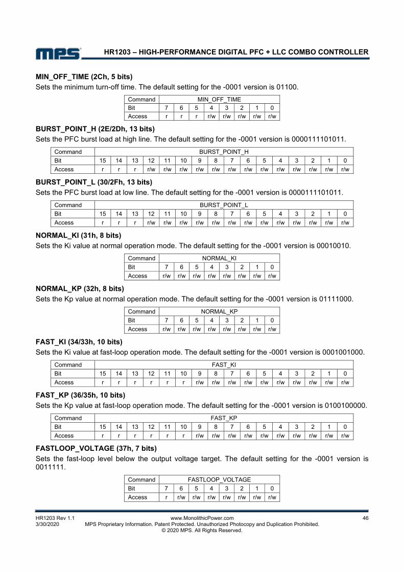
HR1203 – HIGH-PERFORMANCE DIGITAL PFC + LLC COMBO CONTROLLER
HR1203 Rev 1.1 www.MonolithicPower.com 46 3/30/2020 MPS Proprietary Information. Patent Protected. Unauthorized Photocopy and Duplication Prohibited. © 2020 MPS. All Rights Reserved.
MIN_OFF_TIME (2Ch, 5 bits)
Sets the minimum turn-off time. The default setting for the -0001 version is 01100.
Command MIN_OFF_TIME
Bit 7 6 5 4 3 2 1 0
Access r r r r/w r/w r/w r/w r/w
BURST_POINT_H (2E/2Dh, 13 bits)
Sets the PFC burst load at high line. The default setting for the -0001 version is 0000111101011.
Command BURST_POINT_H
Bit 15 14 13 12 11 10 9 8 7 6 5 4 3 2 1 0
Access r r r r/w r/w r/w r/w r/w r/w r/w r/w r/w r/w r/w r/w r/w
BURST_POINT_L (30/2Fh, 13 bits)
Sets the PFC burst load at low line. The default setting for the -0001 version is 0000111101011.
Command BURST_POINT_L
Bit 15 14 13 12 11 10 9 8 7 6 5 4 3 2 1 0
Access r r r r/w r/w r/w r/w r/w r/w r/w r/w r/w r/w r/w r/w r/w
NORMAL_KI (31h, 8 bits)
Sets the Ki value at normal operation mode. The default setting for the -0001 version is 00010010.
Command NORMAL_KI
Bit 7 6 5 4 3 2 1 0
Access r/w r/w r/w r/w r/w r/w r/w r/w
NORMAL_KP (32h, 8 bits)
Sets the Kp value at normal operation mode. The default setting for the -0001 version is 01111000.
Command NORMAL_KP
Bit 7 6 5 4 3 2 1 0
Access r/w r/w r/w r/w r/w r/w r/w r/w
FAST_KI (34/33h, 10 bits)
Sets the Ki value at fast-loop operation mode. The default setting for the -0001 version is 0001001000.
Command FAST_KI
Bit 15 14 13 12 11 10 9 8 7 6 5 4 3 2 1 0
Access r r r r r r r/w r/w r/w r/w r/w r/w r/w r/w r/w r/w
FAST_KP (36/35h, 10 bits)
Sets the Kp value at fast-loop operation mode. The default setting for the -0001 version is 0100100000.
Command FAST_KP
Bit 15 14 13 12 11 10 9 8 7 6 5 4 3 2 1 0
Access r r r r r r r/w r/w r/w r/w r/w r/w r/w r/w r/w r/w
FASTLOOP_VOLTAGE (37h, 7 bits)
Sets the fast-loop level below the output voltage target. The default setting for the -0001 version is 0011111.
Command FASTLOOP_VOLTAGE
Bit 7 6 5 4 3 2 1 0
Access r r/w r/w r/w r/w r/w r/w r/w
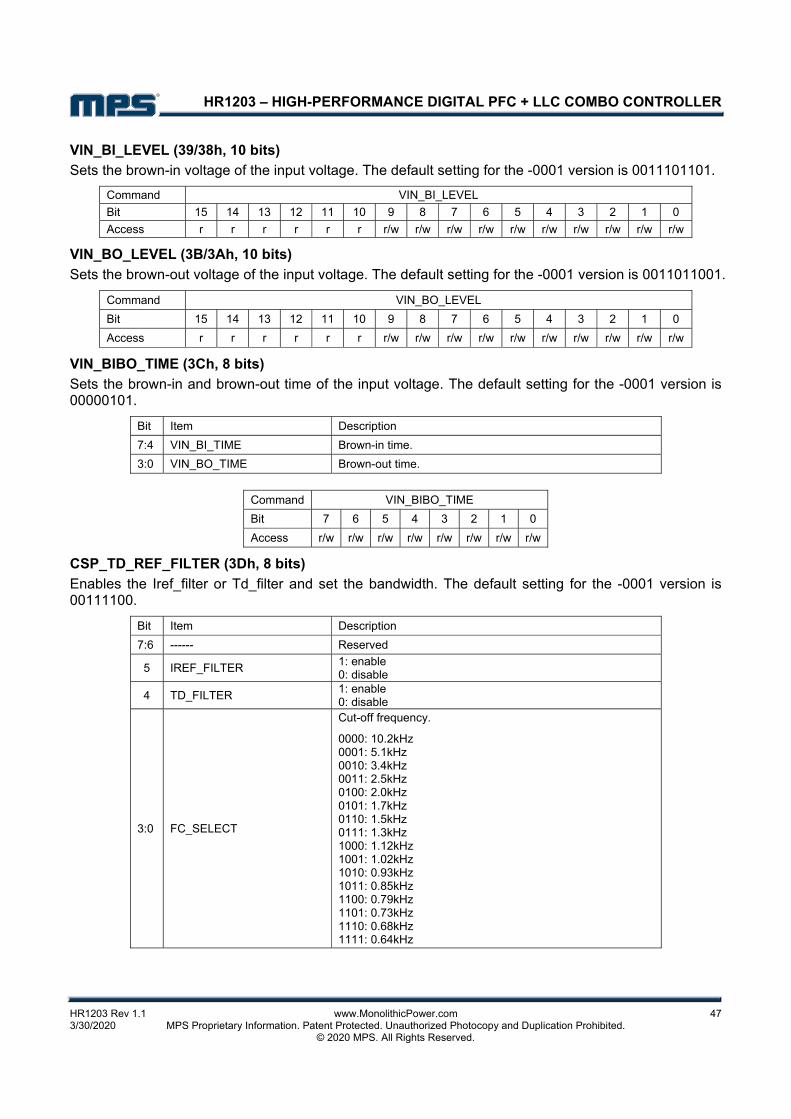
HR1203 – HIGH-PERFORMANCE DIGITAL PFC + LLC COMBO CONTROLLER
HR1203 Rev 1.1 www.MonolithicPower.com 47 3/30/2020 MPS Proprietary Information. Patent Protected. Unauthorized Photocopy and Duplication Prohibited. © 2020 MPS. All Rights Reserved.
VIN_BI_LEVEL (39/38h, 10 bits)
Sets the brown-in voltage of the input voltage. The default setting for the -0001 version is 0011101101.
Command VIN_BI_LEVEL
Bit 15 14 13 12 11 10 9 8 7 6 5 4 3 2 1 0
Access r r r r r r r/w r/w r/w r/w r/w r/w r/w r/w r/w r/w
VIN_BO_LEVEL (3B/3Ah, 10 bits)
Sets the brown-out voltage of the input voltage. The default setting for the -0001 version is 0011011001.
Command VIN_BO_LEVEL
Bit 15 14 13 12 11 10 9 8 7 6 5 4 3 2 1 0
Access r r r r r r r/w r/w r/w r/w r/w r/w r/w r/w r/w r/w
VIN_BIBO_TIME (3Ch, 8 bits)
Sets the brown-in and brown-out time of the input voltage. The default setting for the -0001 version is 00000101.
Bit Item Description
7:4 VIN_BI_TIME Brown-in time.
3:0 VIN_BO_TIME Brown-out time.
Command VIN_BIBO_TIME
Bit 7 6 5 4 3 2 1 0
Access r/w r/w r/w r/w r/w r/w r/w r/w
CSP_TD_REF_FILTER (3Dh, 8 bits)
Enables the Iref_filter or Td_filter and set the bandwidth. The default setting for the -0001 version is 00111100.
Bit Item Description
7:6 ------ Reserved
5 IREF_FILTER 1: enable 0: disable
4 TD_FILTER 1: enable 0: disable
3:0 FC_SELECT
Cut-off frequency.
0000: 10.2kHz 0001: 5.1kHz 0010: 3.4kHz 0011: 2.5kHz 0100: 2.0kHz 0101: 1.7kHz 0110: 1.5kHz 0111: 1.3kHz 1000: 1.12kHz 1001: 1.02kHz 1010: 0.93kHz 1011: 0.85kHz 1100: 0.79kHz 1101: 0.73kHz 1110: 0.68kHz 1111: 0.64kHz

HR1203 – HIGH-PERFORMANCE DIGITAL PFC + LLC COMBO CONTROLLER
HR1203 Rev 1.1 www.MonolithicPower.com 48 3/30/2020 MPS Proprietary Information. Patent Protected. Unauthorized Photocopy and Duplication Prohibited. © 2020 MPS. All Rights Reserved.
Command CSP_TD_REF_FILTER
Bit 7 6 5 4 3 2 1 0
Access r/w r/w r/w r/w r/w r/w r/w r/w
OCP_LIMIT (44h, 7 bits)
Sets the over-current limit of the inductor current. The default setting for the -0001 version is 0000100.
Command OCP_LIMIT
Bit 7 6 5 4 3 2 1 0
Access r r/w r/w r/w r/w r/w r/w r/w
OCP_LIMIT (44h, 7 bits)
Sets the over-current limit of the inductor current. The default setting for the -0001 version is 0000100.
Command OCP_LIMIT
Bit 7 6 5 4 3 2 1 0
Access r r/w r/w r/w r/w r/w r/w r/w
OCP_LIMIT (44h, 7 bits)
Sets the over-current limit of the inductor current. The default setting for the -0001 version is 0000100.
Command OCP_LIMIT
Bit 7 6 5 4 3 2 1 0
Access r r/w r/w r/w r/w r/w r/w r/w
OCP_LIMIT (44h, 7 bits)
Sets the over-current limit of the inductor current. The default setting for the -0001 version is 0000100.
Command OCP_LIMIT
Bit 7 6 5 4 3 2 1 0
Access r r/w r/w r/w r/w r/w r/w r/w
OCP_LIMIT (44h, 7 bits)
Sets the over-current limit of the inductor current. The default setting for the -0001 version is 0000100.
Command OCP_LIMIT
Bit 7 6 5 4 3 2 1 0
Access r r/w r/w r/w r/w r/w r/w r/w
OCP_LIMIT (44h, 7 bits)
Sets the over-current limit of the inductor current. The default setting for the -0001 version is 0000100.
Command OCP_LIMIT
Bit 7 6 5 4 3 2 1 0
Access r r/w r/w r/w r/w r/w r/w r/w
OCP_LIMIT (44h, 7 bits)
Sets the over-current limit of the inductor current. The default setting for the -0001 version is 0000100.
Command OCP_LIMIT
Bit 7 6 5 4 3 2 1 0
Access r r/w r/w r/w r/w r/w r/w r/w

HR1203 – HIGH-PERFORMANCE DIGITAL PFC + LLC COMBO CONTROLLER
HR1203 Rev 1.1 www.MonolithicPower.com 49 3/30/2020 MPS Proprietary Information. Patent Protected. Unauthorized Photocopy and Duplication Prohibited. © 2020 MPS. All Rights Reserved.
OCP_LIMIT (44h, 7 bits)
Sets the over-current limit of the inductor current. The default setting for the -0001 version is 0000100.
Command OCP_LIMIT
Bit 7 6 5 4 3 2 1 0
Access r r/w r/w r/w r/w r/w r/w r/w
OCP_MODE (45h, 4 bits)
Sets the over-current protection mode. The default setting for the -0001 version is 0000.
Bit Item Description
3 OCP_MODE_EN 1: enable 0: disable
2:0 OCP_MODE 000: latch 111: hiccup other: retry number
Command OCP_MODE
Bit 7 6 5 4 3 2 1 0
Access r r r r r/w r/w r/w r/w
OCP_RETRY_DELAY (47/46h, 10 bits)
Sets the delay time of the system recovery after the OCP event is cleared. The default setting for the -0001 version is 0111110100.
Command OCP_RETRY_DELAY
Bit 15 14 13 12 11 10 9 8 7 6 5 4 3 2 1 0
Access r r r r r r r/w r/w r/w r/w r/w r/w r/w r/w r/w r/w
OVP_LIMIT_H (48h, 7 bits)
Sets the over-voltage limit of the output voltage at high line. The default setting for the -0001 version is 1101101.
Command OVP_LIMIT_H
Bit 7 6 5 4 3 2 1 0
Access r r/w r/w r/w r/w r/w r/w r/w
OVP_LIMIT_L (49h, 7 bits)
Set the over-voltage limit of the output voltage at low line. The default setting for the -0001 version is 1101101.
Command OVP_LIMIT_L
Bit 7 6 5 4 3 2 1 0
Access r r/w r/w r/w r/w r/w r/w r/w
CODE ID (4Ah, 8 bits)
Stores customer code ID. The default setting for the -0001 version is 00000001.
Bit Item Description
7:2 CUSTOMER_ID Customer number
1:0 PROGRAMMED CODE_ID Programmed code number
Command CODE ID
Bit 7 6 5 4 3 2 1 0
Access r/w r/w r/w r/w r/w r/w r/w r/w

HR1203 – HIGH-PERFORMANCE DIGITAL PFC + LLC COMBO CONTROLLER
HR1203 Rev 1.1 www.MonolithicPower.com 50 3/30/2020 MPS Proprietary Information. Patent Protected. Unauthorized Photocopy and Duplication Prohibited. © 2020 MPS. All Rights Reserved.
IREF_COMP_VALUE1 (4Bh, 7 bits)
Sets the first compensation amplitude of the input current reference. The default setting for the -0001 version is 0000001.
Command IREF_COMP_VALUE1
Bit 7 6 5 4 3 2 1 0
Access r r/w r/w r/w r/w r/w r/w r/w
IREF_COMP_VALUE2 (4Ch, 7 bits)
Sets the second compensation amplitude of the input current reference. The default setting for the -0001 version is 0000011.
Command IREF_COMP_VALUE2
Bit 7 6 5 4 3 2 1 0
Access r r/w r/w r/w r/w r/w r/w r/w
IREF_COMP_VALUE3 (4Dh, 7 bits)
Sets the third compensation amplitude of the input current reference. The default setting for the -0001 version is 0001101.
Command IREF_COMP_VALUE3
Bit 7 6 5 4 3 2 1 0
Access r r/w r/w r/w r/w r/w r/w r/w
IREF_COMP_VALUE4 (4Eh, 7 bits)
Sets the fourth compensation amplitude of the input current reference. The default setting for the -0001 version is 0001100.
Command IREF_COMP_VALUE4
Bit 7 6 5 4 3 2 1 0
Access r r/w r/w r/w r/w r/w r/w r/w
VIN_LEVEL_SEL1 (4Fh, 8 bits)
Sets the first voltage level of the input voltage. The default setting for the -0001 version is 10011001.
Command VIN_LEVEL_SEL1
Bit 7 6 5 4 3 2 1 0
Access r/w r/w r/w r/w r/w r/w r/w r/w
VIN_LEVEL_SEL2 (50h, 8 bits)
Sets the second voltage level of the input voltage. The default setting for the -0001 version is 01001000.
Command VIN_LEVEL_SEL2
Bit 7 6 5 4 3 2 1 0
Access r/w r/w r/w r/w r/w r/w r/w r/w
VCOMP_MAX_L (52/51h, 16 bits)
Sets the maximum load. The default setting for the -0001 version is 0110110011010010.
Command VCOMP_MAX_L
Bit 15 14 13 12 11 10 9 8 7 6 5 4 3 2 1 0
Access r/w r/w r/w r/w r/w r/w r/w r/w r/w r/w r/w r/w r/w r/w r/w r/w
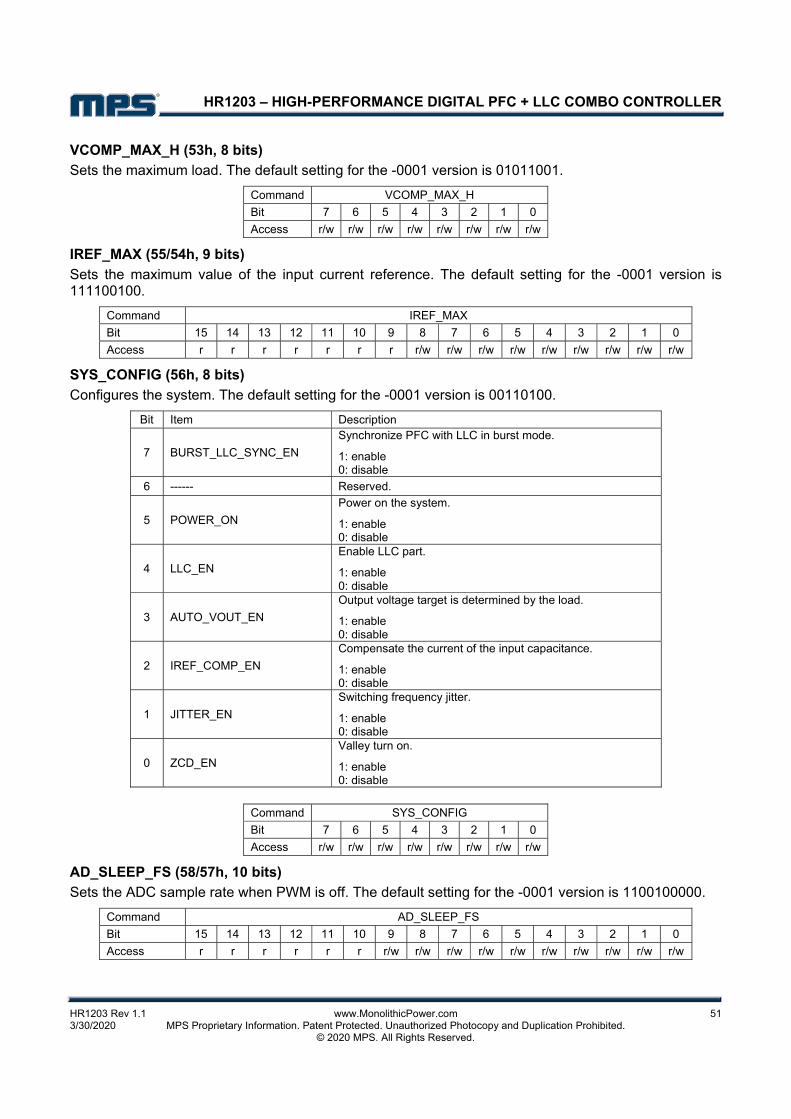
HR1203 – HIGH-PERFORMANCE DIGITAL PFC + LLC COMBO CONTROLLER
HR1203 Rev 1.1 www.MonolithicPower.com 51 3/30/2020 MPS Proprietary Information. Patent Protected. Unauthorized Photocopy and Duplication Prohibited. © 2020 MPS. All Rights Reserved.
VCOMP_MAX_H (53h, 8 bits)
Sets the maximum load. The default setting for the -0001 version is 01011001.
Command VCOMP_MAX_H
Bit 7 6 5 4 3 2 1 0
Access r/w r/w r/w r/w r/w r/w r/w r/w
IREF_MAX (55/54h, 9 bits)
Sets the maximum value of the input current reference. The default setting for the -0001 version is 111100100.
Command IREF_MAX
Bit 15 14 13 12 11 10 9 8 7 6 5 4 3 2 1 0
Access r r r r r r r r/w r/w r/w r/w r/w r/w r/w r/w r/w
SYS_CONFIG (56h, 8 bits)
Configures the system. The default setting for the -0001 version is 00110100.
Bit Item Description
7 BURST_LLC_SYNC_EN
Synchronize PFC with LLC in burst mode.
1: enable 0: disable
6 ------ Reserved.
5 POWER_ON
Power on the system.
1: enable 0: disable
4 LLC_EN
Enable LLC part.
1: enable 0: disable
3 AUTO_VOUT_EN
Output voltage target is determined by the load.
1: enable 0: disable
2 IREF_COMP_EN
Compensate the current of the input capacitance.
1: enable 0: disable
1 JITTER_EN
Switching frequency jitter.
1: enable 0: disable
0 ZCD_EN
Valley turn on.
1: enable 0: disable
Command SYS_CONFIG
Bit 7 6 5 4 3 2 1 0
Access r/w r/w r/w r/w r/w r/w r/w r/w
AD_SLEEP_FS (58/57h, 10 bits)
Sets the ADC sample rate when PWM is off. The default setting for the -0001 version is 1100100000.
Command AD_SLEEP_FS
Bit 15 14 13 12 11 10 9 8 7 6 5 4 3 2 1 0
Access r r r r r r r/w r/w r/w r/w r/w r/w r/w r/w r/w r/w

HR1203 – HIGH-PERFORMANCE DIGITAL PFC + LLC COMBO CONTROLLER
HR1203 Rev 1.1 www.MonolithicPower.com 52 3/30/2020 MPS Proprietary Information. Patent Protected. Unauthorized Photocopy and Duplication Prohibited. © 2020 MPS. All Rights Reserved.
TON_AHEAD (59h, 4 bits)
Sets the peak-current sample point. The default setting for the -0001 version is 0010.
Command TON_AHEAD
Bit 7 6 5 4 3 2 1 0
Access r r r r r/w r/w r/w r/w
OLP_HIGH (5Ah, 7 bits)
Sets the open-loop protection at high level. The default setting for the -0001 version is 1011100.
Command OLP_HIGH
Bit 7 6 5 4 3 2 1 0
Access r r/w r/w r/w r/w r/w r/w r/w
OLP_LOW (5Bh, 7 bits)
Sets the open-loop protection at low level. The default setting for the -0001 version is 0111101.
Command OLP_LOW
Bit 7 6 5 4 3 2 1 0
Access r r/w r/w r/w r/w r/w r/w r/w
SOFT_TON (5Ch, 7 bits)
Sets the soft turn-on time when the system recovers from OVP. The default setting for the -0001 version is 0101000.
Command SOFT_TON
Bit 7 6 5 4 3 2 1 0
Access r r/w r/w r/w r/w r/w r/w r/w
SOFT_SWITCH_CNT (5Dh, 4 bits)
Sets the number of switching events during soft turn on. The default setting for the -0001 version is 0111.
Command SOFT_SWITCH_CNT
Bit 7 6 5 4 3 2 1 0
Access r r r r r/w r/w r/w r/w
MFR_MERGE_REG (5Eh, 8 bits)
The default setting for the -0001 version is 00100001.
Bit Item Description
7:3 SWITCH_BLANK_TIME1 PWM off blanking time
2:1 CURRENT_MIRROR_GAIN
Sets the current mirror gain. The reference current is 62.5µA.
00: GAIN =1 01: GAIN = 1.4 10: GAIN = 1.6 11: GAIN = 2
0 I2C_FILTER_EN
I2C filter.
1: enable 0: disable
Command MFR_MERGE_REG
Bit 7 6 5 4 3 2 1 0
Access r/w r/w r/w r/w r/w r/w r/w r/w

HR1203 – HIGH-PERFORMANCE DIGITAL PFC + LLC COMBO CONTROLLER
HR1203 Rev 1.1 www.MonolithicPower.com 53 3/30/2020 MPS Proprietary Information. Patent Protected. Unauthorized Photocopy and Duplication Prohibited. © 2020 MPS. All Rights Reserved.
SWITCH_BLANK_TIME (5Fh, 8 bits)
Sets the PWM on blanking time. The default setting for the -0001 version is 00110101.
Bit Item Description
7:4 SWITCH_BLANK_TIME2 PWM off blanking time for OCP.
3:0 SWITCH_BLANK_TIME3 PWM off blanking time for OCL.
Command SWITCH_BLANK_TIME
Bit 7 6 5 4 3 2 1 0
Access r/w r/w r/w r/w r/w r/w r/w r/w
OVP_DELAYTIME (60h, 6 bits)
Sets the blanking time of OVP. The default setting for the -0001 version is 110010.
Command OVP_DELAYTIME
Bit 7 6 5 4 3 2 1 0
Access r r r/w r/w r/w r/w r/w r/w
BURST_MODE_HYS (61h, 6 bits)
Sets the hysteresis of the output voltage in burst mode. The default setting for the -0001 version is 001010.
Command BURST_MODE_HYS
Bit 7 6 5 4 3 2 1 0
Access r r r/w r/w r/w r/w r/w r/w
ERROR_ZERO_REGION (62h, 5 bits)
Sets the non-regulation region of the output voltage. The default setting for the -0001 version is 00000.
Command ERROR_ZERO_REGION
Bit 7 6 5 4 3 2 1 0
Access r r r r/w r/w r/w r/w r/w
VIN_ZERO_POINT (63h, 7 bits)
Sets the period detection point of the input voltage. The default setting for the -0001 version is 1010010.
Command VIN_ZERO_POINT
Bit 7 6 5 4 3 2 1 0
Access r r/w r/w r/w r/w r/w r/w r/w
VIN_PEAK_VALUE (64h, 7 bits)
Sets the value to detect the top of the input voltage. The default setting for the -0001 version is 0010100.
Command VIN_PEAK_VALUE
Bit 7 6 5 4 3 2 1 0
Access r r/w r/w r/w r/w r/w r/w r/w
VIN_VALLEY_VALUE (65h, 7 bits)
Sets the value to detect the valley of the input voltage. The default setting for the -0001 version is 0111101.
Command VIN_VALLEY_VALUE
Bit 7 6 5 4 3 2 1 0
Access r r/w r/w r/w r/w r/w r/w r/w

HR1203 – HIGH-PERFORMANCE DIGITAL PFC + LLC COMBO CONTROLLER
HR1203 Rev 1.1 www.MonolithicPower.com 54 3/30/2020 MPS Proprietary Information. Patent Protected. Unauthorized Photocopy and Duplication Prohibited. © 2020 MPS. All Rights Reserved.
IPK_BIAS_TRIM (66h, 8 bits)
Trims the bias voltage at CSP. The default setting for the -0001 version is 00000000.
Bit Item Description
7 CSP_FAULT_MODE
Determine the control mode when CSP is open or shorted.
1: hiccup 0: latch
6 IPK_BIAS_SAMPLE_EN
Enable sampling of the CSP bias voltage when power is on.
1: enable 0: disable
5:0 IPK_BIAS_TRIM Trim the bias voltage at CSP.
Command IPK_BIAS_TRIM
Bit 7 6 5 4 3 2 1 0
Access r/w r/w r/w r/w r/w r/w r/w r/w
ADC_OFFSET_TRIM (67h, 5 bits)
Trims the ADC offset. The default setting for the -0001 version is 00000.
Command ADC_OFFSET_TRIM
Bit 7 6 5 4 3 2 1 0
Access r r r r/w r/w r/w r/w r/w
DELTA_VOLTAGE (68h, 7 bits)
Sets the minimum delta voltage between the input voltage and output voltage for CSP bias voltage sampling. The default setting for the -0001 version is 0101001.
Command DELTA_VOLTAGE
Bit 7 6 5 4 3 2 1 0
Access r r/w r/w r/w r/w r/w r/w r/w
VIN_LEVEL1 (69h, 7 bits)
Input voltage level one for the CSP bias voltage sample. The default setting for the -0001 version is 0010100.
Command VIN_LEVEL1
Bit 7 6 5 4 3 2 1 0
Access r r/w r/w r/w r/w r/w r/w r/w
VIN_LEVEL2 (6Ah, 7 bits)
Input voltage level two for the CSP bias voltage sample. The default setting for the -0001 version is 0101001.
Command VIN_LEVEL2
Bit 7 6 5 4 3 2 1 0
Access r r/w r/w r/w r/w r/w r/w r/w
VIN_LEVEL3 (6Bh, 7 bits)
Input voltage level three for the CSP bias voltage sample. The default setting for the -0001 version is 0111101.
Command VIN_LEVEL3
Bit 7 6 5 4 3 2 1 0
Access r r/w r/w r/w r/w r/w r/w r/w
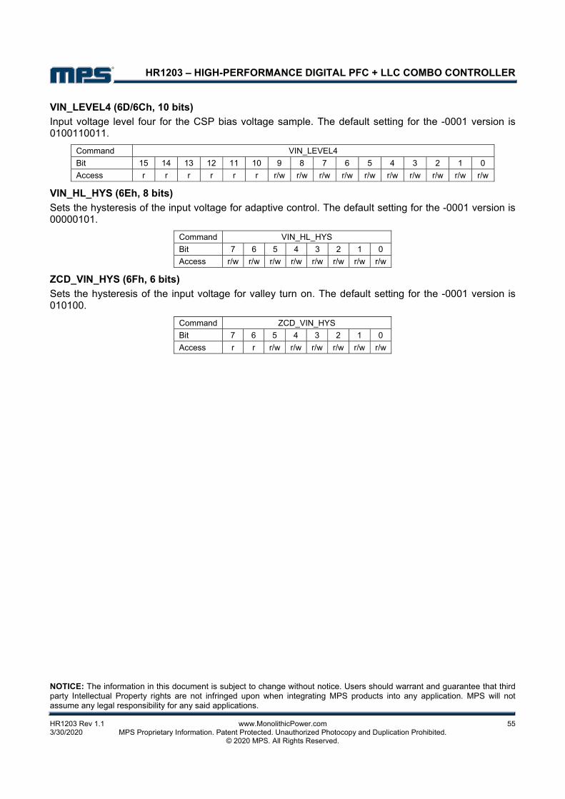
HR1203 – HIGH-PERFORMANCE DIGITAL PFC + LLC COMBO CONTROLLER
NOTICE: The information in this document is subject to change without notice. Users should warrant and guarantee that third party Intellectual Property rights are not infringed upon when integrating MPS products into any application. MPS will not assume any legal responsibility for any said applications.
HR1203 Rev 1.1 www.MonolithicPower.com 55 3/30/2020 MPS Proprietary Information. Patent Protected. Unauthorized Photocopy and Duplication Prohibited. © 2020 MPS. All Rights Reserved.
VIN_LEVEL4 (6D/6Ch, 10 bits)
Input voltage level four for the CSP bias voltage sample. The default setting for the -0001 version is 0100110011.
Command VIN_LEVEL4
Bit 15 14 13 12 11 10 9 8 7 6 5 4 3 2 1 0
Access r r r r r r r/w r/w r/w r/w r/w r/w r/w r/w r/w r/w
VIN_HL_HYS (6Eh, 8 bits)
Sets the hysteresis of the input voltage for adaptive control. The default setting for the -0001 version is 00000101.
Command VIN_HL_HYS
Bit 7 6 5 4 3 2 1 0
Access r/w r/w r/w r/w r/w r/w r/w r/w
ZCD_VIN_HYS (6Fh, 6 bits)
Sets the hysteresis of the input voltage for valley turn on. The default setting for the -0001 version is 010100.
Command ZCD_VIN_HYS
Bit 7 6 5 4 3 2 1 0
Access r r r/w r/w r/w r/w r/w r/w