ht— 2812 1 sound generator - elektronické … · 5 test3 8.488 –32.3 11 test1 12.228 32.3 ......
TRANSCRIPT

A. General Description —
The HT–2812 is a C-MOS LSI chip specially designed for the sound effect
application. It contains only one section which include tone circuit, noise cir-
cuit and other control logic to generate many kinds of sound, such as Rifle
Gun, Machine Gun, Booming Sound, Door Bell, Alarm and etc.... Customer’s
sound source can be analyzed and programmed into internal ROM by changing
one mask layer during device fabrication. It is very suitable for various toy
applications.
B. Features —
• Single power supply: 2.4V ~ 3.3V.
• Low stand-by current at 3V, 1µA typically.
• Auto power-off function.
• Speaker or directly buzzer application.
• Built-in envelop control circuit.
• 1Hz~8Hz programmable LED flash output.
• Minimum external components.
C. Block Diagram —
HT— 2812 APR.15.1993
1 SOUND GENERATOR PAGE: 1

D. Pin Assignment —
E. Pad Assignment & Position —
Chip Size : 67 X 72 (mil)2
* The IC substrate should be connected to VDD in PCB layout artwork.
HT— 2812 APR.15.1993
1 SOUND GENERATOR PAGE: 2

Unit : mil
Pad No. Symbol x Y Pad No. Symbol X Y
1 VSS –27.127 32.3 7 VDD 27.528 –32.3
2 OUT –27.127 –32.3 8 KEY 27.528 –24.65
3 OUT –10.127 –32.3 9 OSC2 27.528 32.3
4 ENV –2.307 –32.3 10 OSC1 19.878 32.3
5 TEST3 8.488 –32.3 11 TEST1 12.228 32.3
6 LED 16.138 –32.3 12 TEST2 4.578 32.3
F. Absolute Maximum Ratings — (Ta=25°C)
Parameter Symbol Minimum Maximum Unit
Supply Voltage VDD –0.3 5 V
Input/Output Voltage VI, VO VSS–0.3 VDD+0.3 V
Storage Temperature TSTG –50 125 °C
Operating Temperature TOP 0 70 °C
G. Electrical Characteristics — (Ta=25°C)
Symbol ParameterTest Condition
Min. Typ. Max. UnitVDD Condition
VDD Operating Voltage 3V — 2.4 3 3.3 V
ISTB Stand-by Current 3V — — 1 5 µA
IDD Operating Current 3V No load — 300 600 µΑ
IOH Output Source Current 3V VOH=2.5V –1 –2 — mA
IOL Output Sink Current 3V VOL=0.5V 1 2 — mA
IENV ENV Source Current 3V VOH=2.5V –1 –2 — mA
ILED LED Source Current 3V VOH=2.5V –1 –2 — mA
HT— 2812 APR.15.1993
1 SOUND GENERATOR PAGE: 3

Symbol ParameterTest Condition
Min. Typ. Max. UnitVDD Condition
FOSC Oscillator Frequency — R=330kΩ — 64 — KHz
VIH "H" Input Voltage 3V — 2.1 — — V
VIL "L" Input Voltage 3V — — — 0.9 V
H. Pad Description —
Pad No. Pad Name I/O Description
1 VSS Negative power supply, GND.
2 OUT O Sound output pad, out of phase to pad 3.
3 OUT O Sound output pad.
4 ENV O Sound envelop control pad.
5 TEST3 I For IC test only.
6 LED O LED flash output pad.
7 VDD Positive power supply.
8 KEY I Key input pad, low active.
9 OSC2 O Oscillator output pad.
10 OSC1 I Oscillator input pad.
11 TEST1 I For IC test only.
12 TEST2 I For IC test only.
HT— 2812 APR.15.1993
1 SOUND GENERATOR PAGE: 4

I. Timing Diagram —
(a) With Envelop :
(b) No Envelop :
HT— 2812 APR.15.1993
1 SOUND GENERATOR PAGE: 5
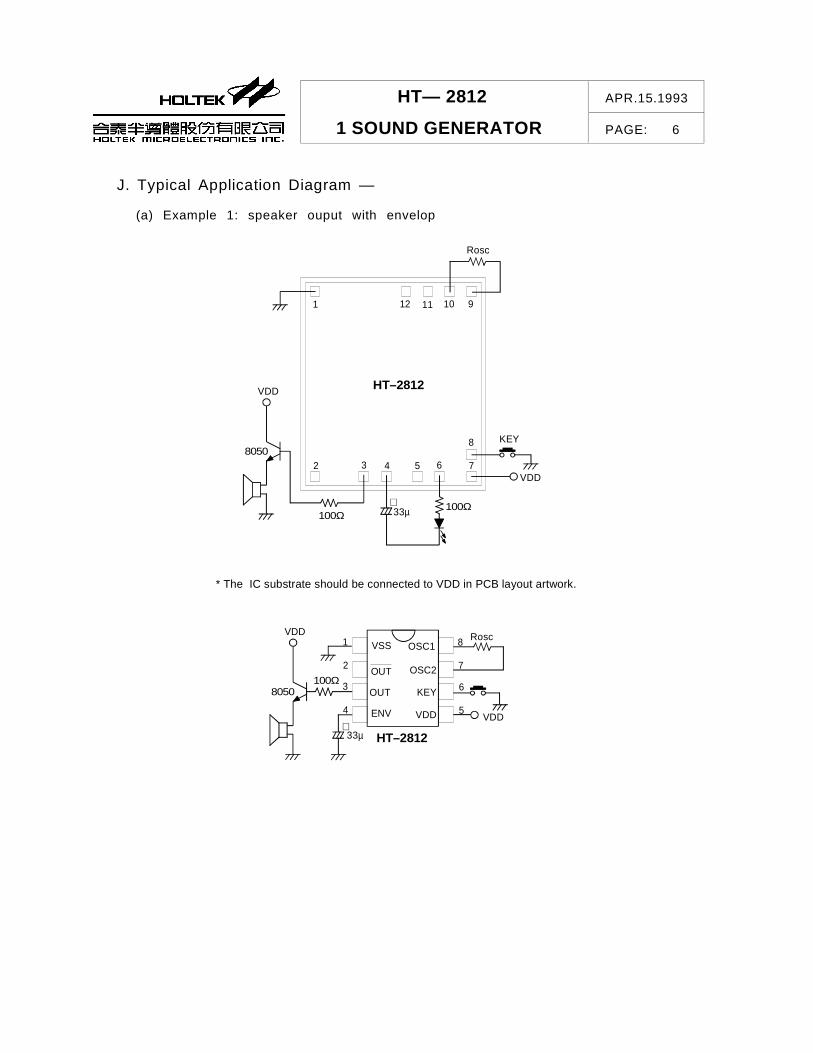
J. Typical Application Diagram —
(a) Example 1: speaker ouput with envelop
HT— 2812 APR.15.1993
1 SOUND GENERATOR PAGE: 6
1
7 2
8
3
9
4
10
5 6
12
HT–2812
8
7
6
5
1
2
3
4
VSS
ENV
OUT
OSC1
OSC2
KEY
VDD
11
Rosc
33µ+ 100Ω
100Ω
VDD
VDD
Rosc
100Ω
8050
VDD
8050
+33µ HT–2812
KEY
VDD
OUT
* The IC substrate should be connected to VDD in PCB layout artwork.

(b) Example 2: speaker output without envelop
HT— 2812 APR.15.1993
1 SOUND GENERATOR PAGE: 7
1
7 2
8
3
9
4
10
5 6
12
HT–2812
8
7
6
5
1
2
3
4
VSS
ENV
OUT
OSC1
OSC2
KEY
VDD
11
Rosc
100Ω100Ω
VDD
VDD
Rosc
100Ω
8050
VDD
8050
HT–2812
100Ω
VDD
OUT
* The IC substrate should be connected to VDD in PCB layout artwork.

(c) Example 3: buzzer output without envelop
HT— 2812 APR.15.1993
1 SOUND GENERATOR PAGE: 8
1
7 2
8
3
9
4
10
5 6
12
HT–2812
8
7
6
5
1
2
3
4
VSS
ENV
OUT
OSC1
OSC2
KEY
VDD
11
Rosc
100Ω
VDD
Rosc
HT–2812
100Ω
Buzzer100Ω
Buzzer
VDD
OUT
* The IC substrate should be connected to VDD in PCB layout artwork.

(d) Example 4: hand touch trigger
HT— 2812 APR.15.1993
1 SOUND GENERATOR PAGE: 9
HandTouch
1
7 2
8
3
9
4
10
5 6
12
HT–2812
8
7
6
5
1
2
3
4
VSS
ENV
OUT
OSC1
OSC2
KEY
VDD
11
Rosc
100Ω
VDD
Rosc
HT–2812
100Ω
Buzzer100Ω
Buzzer
VDD
8050
HandTouch
VDD
8050
VDD
OUT
* The IC substrate should be connected to VDD in PCB layout artwork.
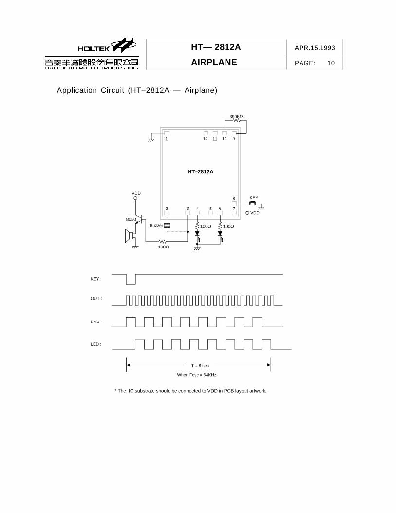
Application Circuit (HT–2812A — Airplane)
HT— 2812A APR.15.1993
AIRPLANE PAGE: 10
1
7 2
8
3
9
4
10
5 6
12
HT–2812A
11
390KΩ
100Ω
VDD
Buzzer 100Ω
KEY
100Ω
VDD
8050
KEY :
OUT :
ENV :
LED :
T = 8 sec
When Fosc = 64KHz
* The IC substrate should be connected to VDD in PCB layout artwork.

Application Circuit (HT–2812B — Rocket)
HT— 2812B APR.15.1993
ROCKET PAGE: 11
1
7 2
8
3
9
4
10
5 6
12
HT–2812B
11
220KΩ
100Ω
VDD
Buzzer 100Ω
KEY
100Ω
VDD
8050
KEY :
OUT :
ENV :
LED :
T = 4.7 sec
When Fosc = 96KHz
* The IC substrate should be connected to VDD in PCB layout artwork.

Application Circuit (HT–2812C — Siren II)
HT— 2812C APR.15.1993
SIREN II PAGE: 12
1
7 2
8
3
9
4
10
5 6
12
HT–2812C
11
390KΩ
100Ω
VDD
Buzzer 100Ω
KEY
100Ω
VDD
8050
KEY :
OUT :
ENV :
LED :
T = 0.45 sec
When Fosc = 64KHz
* The IC substrate should be connected to VDD in PCB layout artwork.
(repeat 15 cycle)

Application Circuit (HT–2812D — Police Car)
HT— 2812D APR.15.1993
POLICE CAR PAGE: 13
1
7 2
8
3
9
4
10
5 6
12
HT–2812D
11
150KΩ
100Ω
VDD
Buzzer 100Ω
KEY
100Ω
VDD
8050
KEY :
OUT :
ENV :
LED :
T = 0.35 sec
When Fosc = 128KHz
* The IC substrate should be connected to VDD in PCB layout artwork.
(repeat 15 cycle)

Application Circuit (HT–2812E — Fire Brigade)
HT— 2812E APR.15.1993
FIRE BRIGADE PAGE: 14
1
7 2
8
3
9
4
10
5 6
12
HT–2812E
11
150KΩ
100Ω
VDD
Buzzer 100Ω
KEY
100Ω
VDD
8050
KEY :
OUT :
ENV :
LED :
T = 4.0 sec
When Fosc = 128KHz
* The IC substrate should be connected to VDD in PCB layout artwork.

Application Circuit (HT–2812G — Siren I)
HT— 2812G APR.15.1993
SIREN I PAGE: 15
1
7 2
8
3
9
4
10
5 6
12
HT–2812G
11
390KΩ
100Ω
VDD
Buzzer 100Ω
KEY
100Ω
VDD
8050
KEY :
OUT :
ENV :
LED :
T = 0.38 sec
When Fosc = 64KHz
* The IC substrate should be connected to VDD in PCB layout artwork.
(repeat 15 cycle)

Application Circuit (HT–2812H — Dialing Tone)
HT— 2812H APR.15.1993
DIALING TONE PAGE: 16
1
7 2
8
3
9
4
10
5 6
12
HT–2812H
11
390KΩ
100Ω
VDD
Buzzer
100Ω
KEY
100Ω
VDD
8050
KEY :
OUT :
LED :
T = 2.5 sec
When Fosc = 64KHz
* The IC substrate should be connected to VDD in PCB layout artwork.
8
7
6
5
1
2
3
4
VSS
ENV
OUT
OSC1
OSC2
KEY
VDD100Ω
VDD
8050
HT—2812H
T = 1.54 sec
390KΩ
OUT
VDD

Application Circuit (HT–2812J — Chicken Sound)
HT— 2812J APR.15.1993
CHICKEN PAGE: 17
1
7 2
8
3
9
4
10
5 6
12
HT–2812J
11
62KΩ
100Ω
VDD
Buzzer
KEY
100Ω
VDD
8050
KEY :
OUT :
LED :
T = 150 sec
When Fosc = 260KHz
* The IC substrate should be connected to VDD in PCB layout artwork.
T = 230 sec

Application Circuit (HT–2812K — Ambulance Sound)
HT— 2812K APR.15.1993
AMBULANCE SOUND PAGE: 18
1
7 2
8
3
9
4
10
5 6
12
HT–2812K
11
390KΩ
100Ω
VDD
Buzzer 100Ω
KEY
100Ω
VDD
8050
KEY :
OUT :
ENV :
LED :
T = 1.9 sec
When Fosc = 64KHz
* The IC substrate should be connected to VDD in PCB layout artwork.
(repeat 3 cycle)