husni habal for the degree of master of science in
TRANSCRIPT

AN ABSTRACT OF THE THESIS OF
Husni Habal for the degree of Master of Science in Electrical and Computer
Engineering presented on July 9, 2004.
Title: Accurate and Efficient Simulation of Synchronous Digital Switching Noise in
Systems on a Chip
Abstract approved:
Kartikeya Mayaram Tern
A new method is presented to compress switching information in large digital
circuits. This is combined with an efficient approach of generating the noise
signatures of cells in a digital library that results in an accurate and efficient approach
for estimating the noise generated in digital circuits. This method provides a practical
approach to generating the digital switching noise for simulating substrate coupling
noise in mixed-signal ICs. Orders of magnitude reduction in the memory and
simulation time are achieved using this approach without significant loss of accuracy.
Redacted for Privacy Redacted for Privacy

© Copyright by Husni Habal
July 9, 2004
All Rights Reserved

Accurate and Efficient Simulation of Synchronous Digital Switching Noise inSystems on a Chip
by
Husni Habal
A THESIS
submitted to
Oregon State University
in partial fulfillment of
the requirements for the
degree of
Master of Science
Presented July 9, 2004
Commencement June 2005
Master of Science thesis of Husni Habal presented on July 9, 2004
APPROVED:
Co-Major Electrical and Computer Engineering
Co-Major Professor, represting Electrical and Computer Engineering
Director of the School of Elfrical Engineering and Computer Science
Dean of the Gradte School
I understand that my thesis will become part of the permanent collection of Oregon
State University libraries. My signature below authorizes release of my thesis to any
reader upon request.
Husni Habal, Author
Redacted for Privacy
Redacted for Privacy
Redacted for Privacy
Redacted for Privacy
Redacted for Privacy

ACKNOWLEDGEMENTS
I shall start by thanking the entire electrical engineering faculty at Oregon
State University for providing an excellent learning and research environment and for
helping me improve my understanding of the various topics of electrical engineering.
In particular, I would like to thank my advisors, Dr. Tern Fiez and Dr. Kartikeya
Mayaram, for supporting my work and for their advice, patience and encouragement
during my studies at Oregon State.
I would also like to thank SRC (Semiconductor Research Corporation) and
DARPA (Defense Advanced Research Projects Agency) for providing my financial
support for this project.
My experience at OSU was enhanced greatly by the company of all my
colleagues in the analog mixed signal group. I am greatly thankful to Shu-Ching Hsu,
Patrick Birrer, Chenggang Xu, Brian Owens, and Sirisha Adluri for their cooperation
and helpful discussions on the substrate noise coupling project. I also appreciate the
help of Robert Batten, James Ayers and Scott Hazenboom with circuit measurements
and laboratory work. Many thanks also to Martin held, HuiEn Pham, Sasi Kumar
Arunachalam, Prasad Talasila, Paul Hutchinson, and all the other people in the analog
mixed signal group that I have failed to mention here.
I would also like to thank the office staff in the Electrical Engineering
department for their help and assistance. In particular, I would like to thank Ferne

11
Simendinger for her help on many occasions in taking care of tedious but essential
office paperwork.
Finally, I would like to thank my parents, Khaled and Amira Habal, for their
love and support.
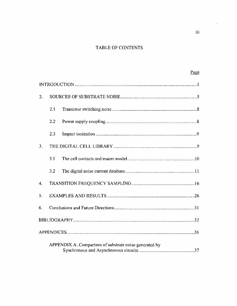
TABLE OF CONTENTS
111
Page
INTRODUCTION......................................................................................................... 1
2. SOURCES OF SUBSTRATE NOISE .................................................................. 5
2.1 Transistor switching noise ......................................................................... 8
2.2 Power supply coupling ............................................................................... 8
2.3 Impact ionization .......................................................................................9
3. THE DIGITAL CELL LIBRARY ........................................................................9
3.1 The cell contacts and macro model .......................................................... 10
3.2 The digital noise current database ............................................................ 11
4. TRANSITION FREQUENCY SAMPLING ...................................................... 16
5. EXAMPLES AND RESULTS ........................................................................... 26
6. Conclusions and Future Directions ..................................................................... 31
BIBLIOGRAPHY ........................................................................................................32
APPENDICES............................................................................................................. 36
APPENDIX A. Comparison of substrate noise generated bySynchronous and Asynchronous circuits................................................ 37

LIST OF FIGURES
Figure
lv
1.1 Basic digital design flow....................................................................................... 3
2.1 Schematic of a simple inverter .............................................................................. 6
2.2 Schematic of a simple inverter with the nodes labeled with the same names usedto define their equivalent regions on the circuit layout shown in Figure 2.3 ........ 7
2.3 The layout of a simple inverter with the contact regions used to connect thecircuit to the substrate network and ground/Vdd defined..................................... 7
2.4 An inverter with a non-ideal bulk connection and a junction capacitance Cdb
generates switching noise at the bulk. Cdb is included in the BSIM3 model butshown here for illustration purposes ..................................................................... 8
2.5 An inverter with a non ideal ground connection................................................... 9
3.1 The macro model for an inverter. The inverter has two bulk contacts and twosubstrate contacts that connect to the power and substrate networks. Thetransistor is replaced in the macro model by four current sources that representthe currents injected into the four contacts during digital switching .................. 11
3.2 The relation between the switching input and the transition vectors for aninvertercell ......................................................................................................... 12
3.3 Maximum percentage of energy loss as a function of the number of responsesamples saved in the digital library for rise times of 0.5 ns to 10 ns .................. 14
3.4 The memory required to store the noise signature database as a function of themaximum percentage of energy loss allowed due to truncation ......................... 15
4.1 Construction of the noise current waveform at a contact. The noise signal isconstructed through a convolution of an input transition vector and the noiseresponse vector .................................................................................................... 17

LIST OF FIGURES (Continued)
Figure
"A
4.2 The frequency spectrum for the random number generator. The top figure showsthe spectrum obtained by a full SPICE simulation. The middle figure shows thespectrum obtained using frequency sampling with a small window, = 8.tjs. Thebottom figure shows the spectrum obtained using frequency sampling with themaximum window size, p = 256.tics .................................................................... 21
4.3 The time domain signal for the random number generator. The top figure showsthe transient signal obtained by a full SPICE simulation. The middle figureshows the transient signal obtained using frequency sampling with a smallwindow, p = 8.tics. The bottom figure shows the transient signal obtained usingfrequency sampling with the maximum window size, p = 256.tics ...................... 22
4.3 VHDL code for setting the transition sampling time and encoding NAND gatetransitions. Similar code is added for all the other gates in the digital circuit. ... 24
4.4 Revised digital design flow with efficient digital noise estimation .................... 25
5.1 Digital Block 1: A 21 inverter chain controlled by a flip-flop ........................... 27
5.2 The noise spectrum for the PWM circuit. The top figure shows the spectrumobtained by a full SPICE simulation. The bottom figure shows the spectrumobtained using frequency sampling and p = 6.tics ............................................... 28
5.3 The noise spectrum for the MIPS processor. The top figure shows the spectrumobtained by a full SPICE simulation. The bottom figure shows the spectrumobtained using frequency sampling and = 4.tics ............................................... 29

LIST OF TABLES
Table
vi
5.1 The simulation time and storage space required for the noise estimation of theexample circuits using a full SPICE simulation and noise estimation with fulltransition vectors and frequency sampling......................................................... 30
5.2 The energy loss due to frequency sampling using p = Djics and = 2D.tics for theexamplecircuits .................................................................................................. 30

vii
APPENDIX LIST OF FIGURES
Figure Page
A-i. A generic Threshold gate ................................................................................ 38
A-2. (a) Ideal inverter and (b) inverter with junction capacitance to the substrateand (c) inverter with a non-ideal ground connection ...................................... 40
A-3. The cross section of a heavily doped substrate............................................... 41
A-4. The cross section of a lightly doped substrate ................................................ 42
A-5. The substrate model for two contacts ............................................................. 42
A-6. A block diagram of the Pseudo Random Number Generator Circuits ............ 43
A-7. The sensor amplifier....................................................................................... 45
A-8. Pin model for a pin on the PGA 84 package................................................... 46
A-9. Design and simulation flow for the RNG circuits .......................................... 48
A-iO. (a) The layout of the synchronous Boolean logic circuit, and 10(b) theasynchronous NCL circuit.............................................................................. 49
A-i 1. The model used for the cell in a digital design during simulation .................. 50
A- 12. The horizontal (surface) substrate network between adjacent contacts in adigitalcircuit ................................................................................................... 51
A-13. The bondwire and routing parasitics for the digital and analog blocks.......... 52
A-i4. Diagram of the complete circuit used to measure noise at the output of thesensor amplifier ............................................................................................... 53
A-15. Noise current injected by a single gate due to a change at its input ............... 54
A-16. The frequency response corresponding to the transient of Figure A-iS......... 55
A-17. Noise response of Figure A-is repeated periodically with a frequency Fclk. 56
APPENDIX LIST OF FIGURES (Continued)
Figure
viii
Page
A-18. The corresponding frequency spectrum to the transient of figure A-17......... 56
A-19. Total synchronous transient time response..................................................... 57
A-20. The total noise spectrum in decibels ............................................................... 58
A-21. The asynchronous noise spectrum in dB ........................................................ 59
A-22. The simulated noise spectrum of the synchronous random number generator inaheavily doped substrate................................................................................ 60
A-23. The measured noise spectrum of the synchronous random number generator ina heavily doped substrate ................................................................................ 60
A-24. The simulated noise spectrum of the asynchronous random number generatorin a heavily doped substrate............................................................................ 61
A-25. The measured noise spectrum of the asynchronous random number generatorin a heavily doped substrate............................................................................ 62
A-26. The simulated noise spectrum of the synchronous random number generator ina lightly doped substrate ................................................................................. 63
A-27. The measured noise spectrum of the synchronous random number generator ina lightly doped substrate ................................................................................. 64
A-28. The simulated noise spectrum of the asynchronous random number generatorin a lightly doped substrate............................................................................. 65
A-29. The measured noise spectrum of the asynchronous random number generatorin a lightly doped substrate ............................................................................. 65

ACCURATE AND EFFICIENT SIMULATION OF SYNCHRONOUSDIGITAL SWITCHING NOISE IN SYSTEMS ON A CHIP
1. INTRODUCTION
The drive towards systems on a chip (S0C) in CMOS technology has forced
the integration of digital circuits and analog blocks on to the same silicon substrate.
With scaled CMOS technologies, it is possible to achieve higher functionality and
packing density on a single die. This has presented new challenges for mixed signal
designers. One of these challenges is the estimation of the switching and supply noise
coupled from the digital circuits through the shared silicon substrate into the sensitive
analog and RF blocks [1].
Digital blocks are capacitively coupled to the chip substrate through transistor
junction capacitances and through interconnect and bond-pad capacitances in the
power and ground networks. When a synchronous digital circuit switches, it causes
potential variations across these coupling capacitances as well as injecting current
directly into the substrate. This, in turn, generates noise currents that flow through the
substrate and power networks. Some of this switching current reaches the analog
block transistors through the substrate or through the parasitic capacitance between
the digital and analog power networks. This current may alter the performance of the
analog transistors by changing the transistor body potential and by altering the power

and ground voltage levels [1, 2]. Analog circuits can be very sensitive to noise in their
frequency band of operation.
Certain measures can be taken to reduce the effect of digital noise on the
analog transistors and are discussed in [3, 4]. These include the use of separate
supplies for the digital and analog circuits, the use of grounded die perimeter rings in
heavily doped silicon substrates, and increasing the power supply rejection ratio
(PSRR) of the analog circuits. Such measures may reduce the noise affects on analog
circuits, but they may not be sufficient in all cases. Estimation of the digital switching
noise is needed to avoid performance degradation in RF and mixed signal ICs.
Additionally, in order for adjustments to be made before fabrication, this needs to be
done as part of the design phase.
Previous work characterized the noise of a standard digital cell library [5-15].
This information is then used to estimate the noise injected by a digital block created
using this standard digital library. Cell characterization involves measuring the noise
current injected into the substrate and power supplies as a function of the digital cell
transitions, the input slew rate, the cell load capacitance as well as several other
factors. This information is then stored as a noise signature in the standard cell
library. The stored noise signatures are combined with the results of an event-driven
gate-level simulation of the digital block and a power/substrate circuit model
[1,10,15,16,17] extracted from the chip layout to estimate the noise injected into the
analog nodes of the chip. A simplified digital design flow with integrated noise
estimation using this methodology is shown in Figure 1.1.

Standard Behavioral VHDL Code Cell TimingLogic Cells Models
Logic Synthesizer
Gate-Level VHDL Netlist with Timing Information
Circuit Layoutand Routing
Chip Power! Extract the InputSubstrate TransitionsNetwork
Noise Spectrum at SensitiveAnalog Nodes
Figure 1.1 Basic digital design flow.
Event-DrivenGate-LevelSimulation
Noise Current Database
3
The basic digital design flow begins with a behavioral description of a digital
circuit in a hardware description language (HDL) such as VHDL or Verilog, which is
synthesized into a netlist of standard logic gates. Next the actual gate layouts are
placed and routed on a chip for fabrication. For the purpose of digital noise
estimation, the gate level netlist is simulated using an event driven simulator and the
switching information for each gate in the digital circuit is recorded. The switching
information is used with the noise signatures stored in the cell library to construct the
noise currents injected by the digital block into the substrate and power networks. The

ru
power and substrate networks are extracted from the digital circuit layout. Finally, the
noise currents are added to the power and substrate circuit and the noise at the
important analog nodes is determined.
It is noted that other authors, such as [18] have suggested the use of stochastic
models based on Markov chains to record the average switching activity in each gate
of a digital circuit as an alternative to performing an event-driven gate-level
simulation. This method for digital noise estimation is, however, too slow to be
inserted as a transparent step in the digital design flow of very large digital circuits.
The main reason being the large amount of memory required to store the noise
signatures in the digital cell library in addition to all switching activity of each gate in
the gate-level simulation and the time required to construct the transient noise
signatures from this stored switching activity.
This thesis presents a method to reduce the size of the digital noise signatures
stored in the digital cell library by truncating the length of the noise current responses
based on an energy-loss criteria. The thesis also proposes a method to reduce the
memory and processing time required for modeling switching noise so that it can be
integrated into the digital design flow of synchronous systems. This method is based
on frequency sampling the input transitions of each gate in real-time during a gate-
level simulation of the digital circuit. The frequency sampled input transitions are
combined with the cell noise signatures and the power and substrate networks to
create an approximate noise spectrum that contains only the important frequency
content at any sensitive node on the chip substrate.

5
The thesis is organized as follows. Chapter 2 summarizes the methods through
which digital noise is injected into the power and substrate networks. Chapter 3
details the new components added to the standard cell library for the purpose of noise
estimation. Chapter 4 describes the scheme used to efficiently store the digital
transitions. Chapter 5 applies the new estimation method to example circuits and
compares the results with complete SPICE simulations. Chapter 6 concludes the
thesis.
2. SOURCES OF SUBSTRATE NOISE
A digital circuit is a block in which signals have only two possible values that
represent the two possible logic values. Signals are either high (logic 1) or low (logic
0). During its operation, the signals in a digital circuit switch between these two
alternating values.
A digital circuit, while switching, injects unwanted signals (switching and
supply noise) into the silicon substrate and power distribution networks due to
parasitic elements. This noise may degrade the performance of analog and RF blocks.
Figure 2.1 shows a simple inverter to illustrate the noise mechanism.
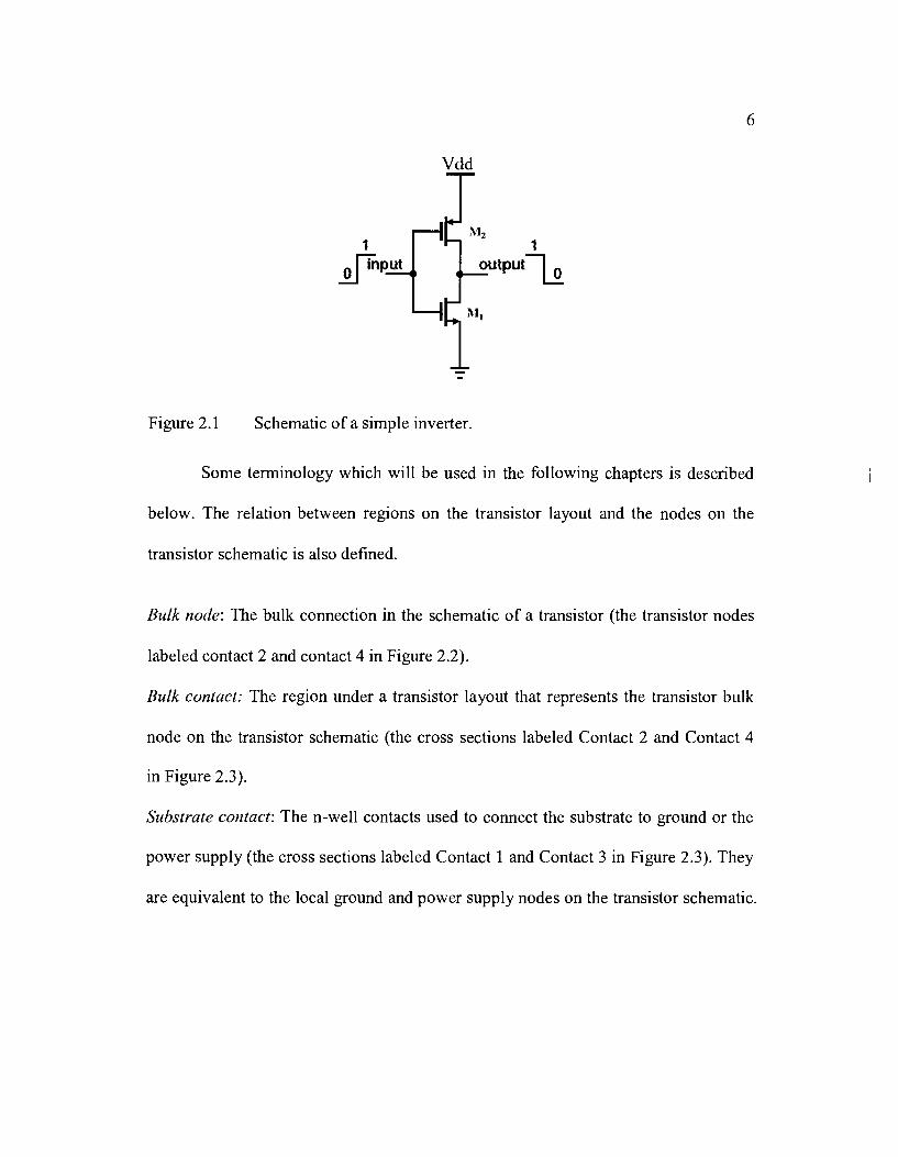
Vdd
I1nPL2UtPut1i
Figure 2.1 Schematic of a simple inverter.
Some terminology which will be used in the following chapters is described
below. The relation between regions on the transistor layout and the nodes on the
transistor schematic is also defined.
Bulk node: The bulk connection in the schematic of a transistor (the transistor nodes
labeled contact 2 and contact 4 in Figure 2.2).
Bulk contact: The region under a transistor layout that represents the transistor bulk
node on the transistor schematic (the cross sections labeled Contact 2 and Contact 4
in Figure 2.3).
Substrate contact: The n-well contacts used to connect the substrate to ground or the
power supply (the cross sections labeled Contact 1 and Contact 3 in Figure 2.3). They
are equivalent to the local ground and power supply nodes on the transistor schematic.

7
contact 3
contact 1
Figure 2.2 Schematic of a simple inverter with the nodes labeled with the samenames used to define their equivalent regions on the circuit layoutshown in Figure 2.3.
tap S Ml D
4-Contact 1 -* active regionContact 2
P-substrate
tapI I
D M2I
S
i-Contact 3-3 active region4 Contact 4
N-well
Figure 2.3 The layout of a simple inverter with the contact regions used toconnect the circuit to the substrate network and groundlVdd.
There are three mechanisms in a digital circuit that contribute to digital noise.
They will be summarized for the NMOS transistor of the inverter of Figure 2.1.

2.1 Transistor switching noise
ml
Vdd
db
Figure 2.4 An inverter with a non-ideal bulk connection and a junctioncapacitance Cdb generates switching noise at the bulk. Cdb is includedin the BSIM3 model but shown here for illustration purposes.
Transistor switching noise occurs when the transistor output changes state.
This state is coupled to the bulk of the transistor through the junction capacitance Cdb
that exists between the drain and bulk of a transistor. The bulk node of a transistor is
generally not ideal, since there is an impedance (typically resistance) between the
substrate and the supply node as indicated in Figure 2.4.
2.2 Power supply coupling
Another source of noise coupling in the bulk is from the power supply.
Typically, the interconnection of the power supply to the digital circuit components,
in addition to the bond pad and chip package parasitics, contribute a parasitic
impedance such as the resistor shown in Figure 2.5. When a current flows through the
circuit transistors a non-ideal voltage will appear at the local supplies due to the
supply parasitics.

Vdd
.itput
Figure 2.5 An inverter with a non ideal ground connection.
2.3 Impact ionization
Impact ionization is another source of substrate noise [19]. It is caused by high
electric fields in the transistor channel close to the drain. When the electric field in the
depleted drain end of a MOS transistor becomes large, the electrons achieve high
velocity and collide with the silicon atoms in the substrate, to create electron hole
pairs. This gives rise to a substrate current. Impact ionization is included in the
BSIM3 standard transistor models. Its effect is small compared to switching noise and
power supply noise. Impact ionization is not studied in the thesis.
3. THE DIGITAL CELL LIBRARY
In order to accurately predict substrate noise in digital circuits, it is necessary
to incorporate both the supply and substrate noise coupling characteristics. These

10
characteristics are added to the digital cell library which is simply a database of all
the digital and 110 cells used to create a digital circuit. It contains a behavioral model
of each cell in addition to input slew rate and load information. The cell library also
contains circuit layouts of the digital cells to be used by the logic synthesis tools.
3.1 The cell contacts and macro model
The bulk and substrate contacts on the layout of the digital cell that are
connected to the power and substrate network are first defined. Each cell contact is
assumed to be a single electrical node connected to the power or substrate network. A
digital cell connects to the power network through its substrate contacts. It connects
to the substrate network through both the substrate contacts and the bulk contacts.
A digital cell is usually small and has only a few transistors. In addition, these
transistors share a single or a few bulk regions that are very close together. If the
resistance of the metal interconnect between substrate contacts within a digital cell is
small, then all the power (or ground) contacts in the digital cell layout are electrically
connected to one power (or ground) node and can be represented by a single cell
contact. It is therefore safe to reduce the number of cell contacts by merging the
transistor bulk contacts in the layout into only a few bulk contacts for NMOS and
PMOS transistors. This approximation is valid independent of the substrate doping
profile. However, if a single cell is large, several bulk contacts may be required to
accurately represent the transistors.
A noise injection macro model for the digital cell can be constructed as shown
in Figure 3.1. For the purpose of noise estimation, the digital cell is replaced by a

11
series of current sources that inject a noise current into each of the cell contact nodes.
The specific values of the macro model current sources are reconstructed from the
digital noise database discussed next.
contact 3
inpu put
I 4
contact 1
Contact 3
13(input)(.1) 14(input)
contact 4 -. Contact 4
contact 2
Contact 1
Figure 3.1 The macro model for an inverter. The inverter has two bulk contactsand two substrate contacts that connect to the power and substratenetworks. The transistor is replaced in the macro model by four currentsources that represent the currents injected into the four contactsduring digital switching.
3.2 The digital noise current database
For each cell in the digital cell library, the noise current signal flowing
through each of the cell contacts must be measured and stored for all possible input
transitions. It will be shown later that if the type and time of the input transitions is
recorded during a simulation of a digital circuit, then the noise currents recorded in
the digital noise current database can be used to reconstruct the digital noise currents
over that same time period to be substituted into the cell macro model.

12
If there are M inputs to a digital cell and two input values {O, 1 }, then the
total number of possible transition types is 2' (2 1). For an inverter there are 2
possible transitions 0 1 and 1 0. Let Gpq[n] be the vector of cell input
transitions for a gate, where p -* q refers to the transition type. The inverter has two
transition types 0 1 and 1 -* 0 and, therefore, two transition vectors G01[n] and
G0[n]. If a transition from 0 1 occurs at time n, then G0[n] = 1, otherwise
G01[n] = o, as shown in Figure 3.2. Each transition type at the inputs of a digital cell
results in a different noise response at each of the cell contacts. Let hpq [n] be the
noise response due to transition p -> q at contact C of a digital cell.
Input
G01 =(X1O10001]Input (0 1010 00 1]
G10 =(X0101000]
Figure 3.2 The relation between the switching input and the transition vectors foran inverter cell.
The noise characteristics are affected by the cell load capacitance and input
slew rate. The transient responses for each possible combination of these factors must
be recorded in the digital cell database. The possible values of the cell load
capacitance and input slew rate are usually known and are part of the digital cell
library timing models. It would be impossible to store the noise current through each
cell contact for all possible cell input transitions and all the independent variables as

13
the memory requirement for the digital cell library would be extremely large. Some
approximations must be made in order to store and handle this large amount of data.
There are many variables that affect the shape of the noise currents. It is
possible to approximate the effect of some of these variables by an equation instead
of storing the complete noise response. The authors of [20] propose the use of an
equation to model the effect of the input slew rate. This approach reduces the
dimension of the noise current database by one.
If it can be determined from the sensitive analog circuits on the chip that the
frequency band of interest can be limited to BW for all the circuits created using the
digital cell library, then the noise response vectors hpq [n] can be limited to the same
bandwidth BW. It follows that hp5q [n] can be reconstructed if it has the sampling
period i/f5, where f5 = 2BW is the Nyquist frequency.
Since memory storage for the digital library is limited, it is necessary to limit
the size of each noise response hpq[fl] while maintaining the shape of the
corresponding power spectrum hp*q (without causing a large loss of noise energy).
If hp>q [n] is truncated to points, then the fraction of energy loss can be defined as
follows.
hp_q[flIdisc(:1ed = hp_q[fl]U[fl N5] (3.1)
energy lost (%) /hp_q[fl]2 xlOO (3.2)
where u{n] denotes the unit step function.

14
Figure 3.3 is a plot of the maximum percentage of energy loss due to
truncation of the output waveform for the digital library described in the next section
while varying the input rise time. The digital cell library contains 25 cells and the
digital noise currents were stored for 7 different rise times using 32 bit floating point
precision. Decreasing the rise time to 0.Sns increases the energy lost to only a few
percent. Storing only 50 samples will result in an energy loss of only 0.05% for the
noise responses with a ins input rise time
100 -------------------------------------------------------- F
1IJ
J)0-J>0)
a)
uJ
a)C.)I.-
a) .01a-
001
000150 100 150200 250 300 350400 450 500
Response Samples Saved (samples)
Figure 3.3 Maximum percentage of energy loss as a function of the number ofresponse samples saved in the digital library for rise times of 0.5 ns toiOns.
Thus, it is concluded that most of the energy in a transition response is
concentrated in the beginning of the response and it is possible to efficiently store the

15
noise response vectors hp*q [ni in the digital cell library by defining a maximum
energy loss, for example 5%, and then truncating each response vector hp.>q[fl] until
its percentage of energy loss is less than 5%. Figure 3.4 shows a plot of the memory
required to store the noise responses as the maximum allowed percentage of energy
loss is varied from .01% to 100% for the digital cell library used in this thesis.
4 1
35----t---.--
o 3
U)
25H
U)
> 2I.. [
oE
15ci) H0) H( H...................o0) H:H
5--------------------------------- -, - ._---0 --.-------___________________________
.01 .1 1 10
Maximum Percent of Energy Lost
Figure 3.4 The memory required to store the noise signature database as afunction of the maximum percentage of energy loss allowed due totruncation.
It is observed from Figure. 3.4 that using energy loss as a measure for
truncating the noise responses hpq [n] can help in significantly reducing the size of
the noise signature database. Storing the noise responses with a .1% maximum energy
16
loss would require 950 MB of memory. Storing the noise responses with a 1%
maximum energy loss would reduce this requirement to 204 MB.
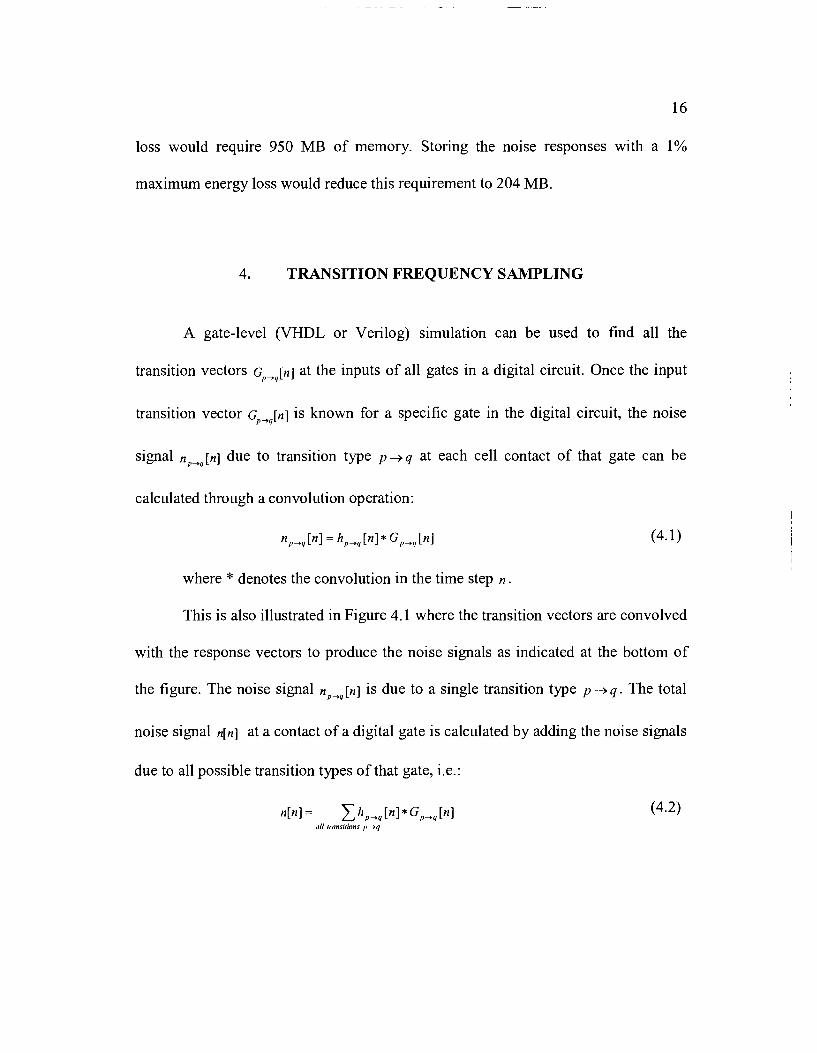
4. TRANSITION FREQUENCY SAMPLING
A gate-level (VHDL or Verilog) simulation can be used to find all the
transition vectors at the inputs of all gates in a digital circuit. Once the input
transition vector Gp.q[fl] is known for a specific gate in the digital circuit, the noise
signal flpq [nJ due to transition type p -* q at each cell contact of that gate can be
calculated through a convolution operation:
flp_q [n] = [n] * [n] (4.1)
where * denotes the convolution in the time step n.
This is also illustrated in Figure 4.1 where the transition vectors are convolved
with the response vectors to produce the noise signals as indicated at the bottom of
the figure. The noise signal [n] is due to a single transition type p q. The total
noise signal n[n] at a contact of a digital gate is calculated by adding the noise signals
due to all possible transition types of that gate, i.e.:
n[n] = hp_q [n] * [n] (4.2)all transitions ptq

17
Hp4q
/\Vl_._..
Figure 4.1 Construction of the noise current waveform at a contact. The noisesignal is constructed through a convolution of an input transitionvector and the noise response vector.
The noise signals at each contact are then substituted into the cell macro
model discussed in the previous section. Once this is done, it is connected to the chip
power and substrate network and simulated to find the noise at the sensitive analog
nodes.
The method described for calculating the noise current for each contact in a
digital circuit yields results that are consistent with a full SPICE simulation of the
circuit. A problem arises, however, with simulation time and storage memory when
attempting to simulate large digital circuits for extended periods of time, since all the
digital transition information must be stored for the complete gate-level simulation,
thus slowing down the simulation. A simple method is next described that reduces the
amount of memory required to store the transition vectors Gpq[fl] during a gate-level
simulation of a digital circuit. It is shown that the transition vector power is
concentrated at a fundamental frequency and its harmonics. The transition vectors

FI
Gpq[fl] are stored at only this fundamental frequency and its harmonics, i.e., the signal
is sampled at integer multiples of the fundamental frequency.
A synchronous digital circuit consists of synchronously clocked flip-flops.
The path between the circuit flip-flops is comprised of chains of combinational logic
one or several levels deep. The maximum clock frequency at which a digital circuit
can operate correctly is dependent on the longest propagation delay between two flip-
flops or a flip-flop and an 110 port. The propagation delay of a combinational path is
a function of the propagation delay of the gates in that path. The more gates there are,
the larger the propagation delay of the combinational path. Let D represent the length
of the longest path between two flip-flops in a digital circuit operating at a single
clock frequency, f,k It follows that the value of D will usually be small for a well
designed digital circuit running at a high clock frequency. The power in the transition
vector signal spectrums is concentrated at a countable number of frequencies whose
number depends on D . The most extreme case is when some gates in the
combinational path switch rarely during circuit simulation, or more precisely they
switch every 2D clock periods. hi this case the transition vectors Gpq[fl] must be
sampled at a frequency of f / 2D and its harmonics to obtain all the signal energy. A
different function of D may be used for circuits whose gates operate closer to the
clock frequency, f/k For instance a sampling frequency of f,k! D may be used if we
assume that each gate in the combinational path is affected by the clock every D

19
clock cycles. In this case the transition vectors Gpq[fl] are sampled at a frequency of
ffkI D and its harmonics to obtain all the signal energy.
Let F,q[n] be the frequency sampled function of the digital transition vector
Gpq[fl] Fp.q[fl] is calculated from Gpq[fl] as follows:
Fp*q{flI = Gpq[fl +1]ö(n -l.p) (4.3)
Frequency sampling the transition vector Gp.q[flI is done mathematically by
saving a moving average of a fixed length. The length of the moving average is a
function of D, the longest path length between two flip-flops. In the most extreme
case the length is p =2D.tics. In the other suggested casep = D.tics, where tics is the
number of samples per clock period.
is:
The estimated noise current signal (denoted by n[n]) calculated using F,,q[fl]
e[1= h Inl*F [n]pqI- i p*qall fransitions p*q
(4.4)
Let n(w) and fle(W) be the spectrums of n[n] and e[]' respectively. fle(&) will contain
all the important frequency components of n(co). This is demonstrated in Figure 4.2,
which shows the frequency response of a random number generator with p = D.tics
and p = 2'.tics. It is observed from Figure 4.2 that the frequency response from full
SPICE simulation matches the estimated waveform in terms of major frequency
content and amplitude for the two suggested values of p . As for the transient
response, for signals whose period is less than p. the time domain signal is exact.

When this condition is not satisfied, the time domain waveforms after frequency
sampling may not exactly match the original time domain signal. However, the
energy content of the time domain waveform is preserved. If it is necessary to ensure
that the time domain response after frequency sampling exactly matches the original
time domain response, then the most extreme case for the frequency sampling
window must be used (p = 2Dfjcs). Figure 4.3 shows the transient response for the
random number generator from complete SPICE simulation, from frequency
sampling with p = Dtics and from frequency sampling with p = 2D.tics. It is observed
from the case where p = 2Dfics, that the transient response exactly matches the
original signal from SPICE, while, in the case when p = Di ics, the averaging effect of
frequency sampling appears on the time domain signal.
A comparison is made between the memory required to store the full
transition vectors Gp.q[flI and the frequency sampled transition vectors Fq[fl] Let Q
be the total number of gate inputs in a digital circuit, K the number of simulation
clock periods, and tics the number of samples per clock period. The memory
requirement for storing all the input transition vectors Gpq{flI is of the order
O(Q.K.tics). This is a large amount of memory that may slow down the gate-level
simulation of the digital circuit. The memory needed to store the frequency sampled
transition vectors Fq[n] is O(Q.p) and is independent of the simulation time.
However, when a larger frequency sampling window p is used the required memory
is larger, and the reduction in needed memory and simulation time will be less.

Spice Simulation
>1
: L J II J J J i0 20 40 60 80 100 120 140 160 180 200
Noise Estimation with Frequency Sampling (p = 8*tics)6 ... ____ ____ . ____
>
ULI II{IIIhInLi hi L11IIhIFlI11IIlIiIIill
0 20 40 60 80 100 120 140 160 180 200Noise Estimation with Frequency Sampling (p = 256*tics)
6
5'U)
:W 1J l±)O) 20 40 60 80 100 120 140 160 180 2(
Frequency (MHz)
21
Figure 4.2 The frequency spectrum for the random number generator. The topfigure shows the spectrum obtained by a full SPICE simulation. Themiddle figure shows the spectrum obtained using frequency samplingwith a small window, p = 8.tics. The bottom figure shows the spectrumobtained using frequency sampling with the maximum window size,p = 256.tics.

>
a)
0)
>
a)
C0)
____- ____H____ H0 2 4 6 8 10 12 14 16 18
Spice Simulation
0 2 4 6 8 10 12 14 16 18 20Noise Estimation with Frequency Sampling (p = 8*tics)
>E4a)
C0)
Noise Estimation with Frequency Sampling (p = 256*tics)
0 2 4 6 8 10 12 14 16 18 20Time (us)
22
Figure 4.3 The time domain signal for the random number generator. The topfigure shows the transient signal obtained by a full SPICE simulation.The middle figure shows the transient signal obtained using frequencysampling with a small window, p = 8.tics. The bottom figure shows thetransient signal obtained using frequency sampling with the maximumwindow size, p = 256.tics.
Frequency sampling of the transition matrix must be accomplished during the
gate-level simulation of the digital circuit. The best method to accomplish this
23
without dependence on the simulation program used in this work is to embed the
sampling program into the structural VHDL (or Verilog) code of the simulated
circuit. The sampling program runs as part of the gate-level simulation and collects
and encodes the transition information without affecting the digital circuit simulation.
Figure 4.3 shows a section of the code in VHDL for a digital circuit. It elaborates the
embedded code used to encode the transition information for an inverter gate.

architecture struct of digital_circuit isvariable next_tic : Integer := 0;variable tic : Integer := 0;variable transition: Integer := 0;
transition samples = 300, INVO1 transition types = 2type INVO1_transitions is array(0 to 299,0 to 1) of Integer;
variable tran_ixl4l4 : INVO1_transitions := (OTHERS => (OTHERS >
0));transition matrices for other gates created
component INVO1port
Y : OUT std_logicAU : IN std_logic
end componentother component declarations
signal OUT1, IN1: std_logicother signals
beginset up the transition sampling time
process (next_tic)begin
next_tic := (tic + 1) mod 300;tic := next_tic after 1 ns;
end process;NAND gates:
declaration and transition matrix for Inverter cell "gatel"gatel : INVU1 port map ( Y=>OUT1, A0=>INl);process (tic)begin
simple transition encodingtransition := stdlogic2integer(transition & IN1, 4);tran_ix1414(tic,transition) := tran_ix1414(tic,transition) + 1;
end process;other Inverter gate instantiationsother cell types
end struct
Figure 4.4 VHDL code for setting the transition sampling time and encodingNAND gate transitions. Similar code is added for all the other gates inthe digital circuit.
Other more intricate methods for encoding the transition information have
been studied, including the use of wavelets to compress the transition matrix [21] and
Wiener filters for transition matrix encoding and estimation [221. Frequency

25
sampling, however, offers a very efficient encoding method that is fast, accurate, and
works for all synchronous digital circuits.
Standard Behavioral VHDL Code Cell TimingLogic Cells Models
ILogic Synthesizer
Gate-Level VHDL Netlist with Timing Information
I I Structural NetlistwithCircuit Layout 1 I
Frequency
H Frequency SamplingEmbeddedand Routing Sampling
Function
Chip Power/ Extract the InputSubstrate TransitionsNetwork
Noise Spectrum at SensitiveAnalog Nodes
Event-DrivenGate-LevelSimulation
Noise Current Database
Figure 4.5 Revised digital design flow with efficient digital noise estimation.
The full digital transition flow of Figure 1.1 can now be modified to include
transition estimation as shown in Figure 4.4. In Figure 4.4, after a gate level netlist of
the digital circuit is created and before the event-driven simulation is performed,
additional frequency sampling functions are added to the code to measure and
frequency-sample all the gate inputs in the circuit.

26
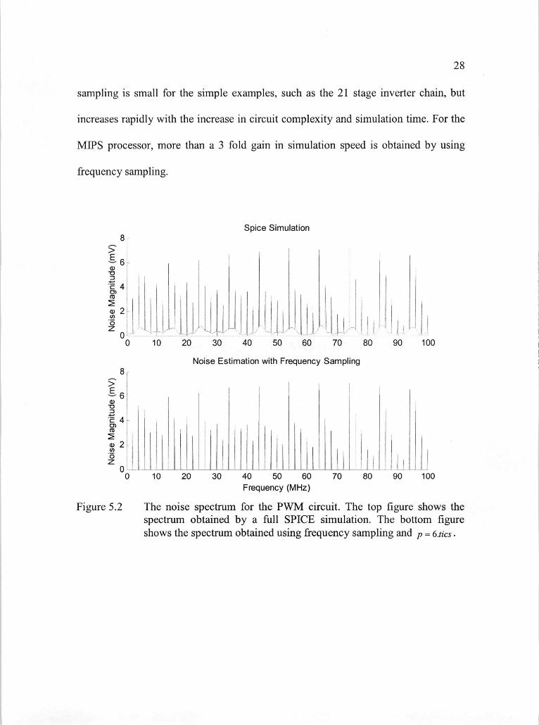
5. EXAMPLES AND RESULTS
Several examples are used to demonstrate the new noise estimation method.
Each example is comprised of a digital block and a simple analog circuit, in this case,
a single-ended operational amplifier. These examples illustrate how this approach can
be used in mixed signal ICs and, because it is general, it can be applied to a range of
analog circuits with different frequencies of interest. The amplifier in this example is
connected in a unity gain feedback and the digital noise propagated to its bulk region
through the power and substrate network is calculated. These examples are used to
illustrate the digital noise simulation technique and not to study its impact on analog
circuits.
The first digital block is a ring of 21 inverters and a flip-flop as shown in
Figure 5.1. The second digital block is a simple 8-bit counter. The third digital circuit
is a pulse width modulator (PWM) and consists of a 12 bit counter, three 8 bit
registers and a simple state machine. There are 42 flip-flops and 234 combinational
gates in the PWM block. The fourth circuit is an 8-bit pseudo random number
generator (RNG). It consists of an 8 bit register, adder and multiplier. The fifth circuit
is a small MIPS processor with a 10-bit instruction path and an 8-bit data path. The
processor consists of 260 flip-flops and 831 logic gates.

27
HDQclk 21 inverters
Figure 5.1 Digital Block 1: A 21 inverter chain controlled by a flip-flop.
A complete SPICE simulation of each example circuit is performed and the
digital noise at the analog block is determined. The digital noise is also calculated
using a gate-level simulation with full transition vectors and with frequency sampling.
The computational requirements for the example circuits are presented in Table 5.1.
In addition the total percentage of energy loss in the spectrum due to frequency
sampling for each circuit is presented in Table 5.2 as a measure of accuracy. It is seen
that the storage space required for noise estimation with frequency sampling is
reduced by at least an order of magnitude when compared to SPICE simulation. The
amount of space that is saved through noise estimation with frequency sampling
increases with the length of simulation time. This is in agreement with the previous
section where the storage with frequency sampling is shown to be independent of the
simulation time. This is apparent for the example of the MIPS processor, because the
MIPS processor requires a long simulation time. A simulation speed gain is also
observed for the examples of Table 5.1. The simulation time is reduced by a factor of
4 in the 21 stage inverter chain and by more than a factor of 50 for the MIPS
processor when compared to SPICE simulations. The speed increase for noise
estimation with frequency sampling compared to noise estimation without frequency
sampling is small for the simple examples, such as the 21 stage inverter chain, but
increases rapidly with the increase in circuit complexity and simulation time. For the
MIPS processor, more than a 3 fold gain in simulation speed is obtained by using
frequency sampling.
8
a)
E 40)(0
a) 2Cl)
0z
0 10
8
a)
E 4-0)(0
2U)
z
Figure 5.2
Spice Simulation
LJLLLLIL.JLIL20 30 40 50 60 70 80 90 100
Noise Estimation with Frequency Sampling
ILJh10 20 30 40 50 60 70 80 90 100
Frequency (MHz)
The noise spectrum for the PWM circuit. The top figure shows thespectrum obtained by a full SPICE simulation. The bottom figureshows the spectrum obtained using frequency sampling and p = 6.tics.

30
ELa)
00a)C,,
0z00
30
20a)
0a-ci)
CO
0z00
Figure 5.3
Spice Simulation
20 40 60 80 100 120 140 160 180 200
Noise Estimation with Encoding
20 40 60 80 100 120 140 160 180 200
Frequency (MHz)
The noise spectrum for the MIPS processor. The top figure shows thespectrum obtained by a full SPICE simulation. The bottom figureshows the spectrum obtained using frequency sampling and = 4.tics.
The frequency spectrum of switching noise from full SPICE simulations and
using the noise estimation techniques described are shown for the random number
generator (RNG) in Figure 4.2, for the PWM circuit, and the MIPS processor in
Figures 5.2 and 5.3, respectively. The top graph in each figure is the noise magnitude
at the sensitive analog bulk connection from a SPICE simulation. The bottom graph is
the estimated noise magnitude with frequency sampling. The full SPICE simulation
calculates the noise at a large number of points on the noise spectrum where noise
magnitude may or may not be significant. The noise estimation method calculates the
noise magnitude at only the points on the spectrum where large spikes occur. It is
seen from the graphs and from the percentage of energy loss in Table 5.2 that the
proposed method of frequency sampling is accurate as it captures all the important

iIiJ
noise information in the frequency spectrum. The error in the spectrum magnitudes at
the frequencies of interest for each graph using the frequency sampling approach is
less than three percent when compared to the full SPICE simulation.
Table 5.1 The simulation time and storage space required for the noiseestimation of the example circuits using a full SPICE simulation andnoise estimation with full transition vectors and frequency sampling.
Simulation Time (s) Storage (MB)
Frequency Sampled Frequency SampledFull Transition Vectors Full Transition Vectors
SPICE Transition SPICE TransitionVectors Vectors
D.tics 2 D .tics D.tics 20 tics
21 StageInverter 630 312 256 256 24.1 6.72 1.344 1.344Chain_______8bit 2020 643 476 510 101 29.8 5.97 15.8Counter
PWM 37254 7900 3025 5630 1300 879 44 450
RNG 9130 3400 2081 3400 964 890 35 890
MIPS 579200 31618 9854 13560 14333 3600 175 720
Table 5.2 The energy loss due to frequency sampling using = Diics and= 2Dj1CS for the example circuits.
% Total Energy Loss due to Frequency Sampling
E
p = D.tics p = 2°.tics
21 Stage Inverter Chain .021 0
8 bit Counter .950 .02
PWM 1.224 .09
RNG 2.84 0
MIPS .0311 .001

31
6. CONCLUSIONS AND FUTURE DIRECTIONS
In this thesis techniques are presented for efficient storage of the digital noise
signatures generated by the cells in a digital library. It is possible to significantly
truncate the length of the noise signatures without losing important information in the
noise frequency spectrum. A method is also described to sample the digital switching
information that occurs during a gate-level simulation of synchronous digital circuits
at only the important high energy frequencies. This allows the switching information
for digital circuits with very large gate counts and very long simulation times to be
stored without slowing down the gate-level simulation. Sampling is performed on the
switching information independent of the digital simulator used. It is done by adding
the code to compress and store the switching information directly to the digital
VHDL code of the digital circuit. The sampled switching information is used with the
noise current database to create an estimate of the noise generated by the digital
circuit. Several example designs are created that show the accuracy of the new noise
estimation method as well as the significant memory savings due to compression. The
new noise estimation method is added as a standard step in the digital design flow.
Future work can be directed towards integrating the new noise estimation
method into commonly used design tools, such as the Cadence design environment.
The new noise estimation method can also be used as a tool to quickly verify new
methods for reducing the amount of noise generated by switching digital circuits,
such as testing different layout configurations for the digital circuits and optimizing
the digital synthesis code for noise reduction.

32
BIBLIOGRAPHY
[1] N. K. Verghese, T. J. Schmerbeck, D. J. Alistot, "Simulation Tecimiques andSolutions for Mixed-Signal Coupling in Integrated Circuits," Kiuwer AcademicPublishers, 1995.
[2] CADENCE, Substrate Coupling Analysis User Guide, Product Version 4.4.6,April 2001.
[3] B. Owens, P. Birrer, S. Adluri, R. Shreeve, S. A. Arunachalam, H. Habal, S.Hsu, A. Sharma, K. Mayaram, and T. Fiez, "Strategies for simulation,measurement and suppression of digital noise in mixed-signal circuits," CustomIntegrated Circuits Conference, Sept. 2003, pp. 36 1-364.
[4] Y. Zinzius, E. Lauwers, G. Gielen, and W. Sansen, "Evaluation of substratenoise effect on analog circuits in mixed-signal designs," 2000 SouthwestSymposium on Mixed-Signal Design, Feb. 2000, pp. 131-134.
[5] K. C. Wen, N. Verghese, H.-Y, Cho, K. Shimazaki, H. Tsujikawa, S. Hirano, S.Doushoh, M. Nagata, A. Iwata, and T. Ohm, "A substrate noise analysismethodology for large-scale mixed-signal ICs," Custom Integrated CircuitsConference., 2003, pp. 369-372.
[6] M. Nagata, K. Hijikata, J. Nagai, T. Morie, and A. Iwata, "Reduced substratenoise digital design for improving embedded analog performance," IEEEInternational Solid-State Circuits Conference, Feb. 2000, pp. 224-225.
[7] P. Miliozzi, L. Carloni, E. Charbon, and A. Sangiovanni Vincentelli,"SUBWAVE: a methodology for modeling digital substrate noise injection inmixed-signal ICs," Custom Integrated Circuits Conference, May 1996, pp. 385-388.
[8] M. V. Heijningen, J. Compiet, P. Wambacq, and S. Donnay, "Modeling ofdigital substrate noise generation and experimental verification using a novelsubstrate noise sensor," Proc. ESSCIRC, Sept. 1999, pp. 186-189.
[9] M. Nagata, T. Morie, and A. Iwata, "Modeling substrate noise generation inCMOS digital integrated circuits," Custom Integrated Circuits Conference, May2002, pp. 501-504.
33
[10] M. Xu, D. K. Su, D. K. Shaeffer, T. H. Lee, and B. A. Wooley, "Measuring andmodeling the effects of substrate noise on the LNA for a CMOS GPS receiver,"IEEEJ. Solid-State Circuits, vol. 36, PP. 473-485, March 2001.
[11] E. Charbon, P. Miliozzi, L. P. Carloni, A. Ferrari, and A. Sangiovanni-Vincentelli, "Modeling digital substrate noise injection in mixed-signal IC's,"IEEE Transactions on Computer-Aided Design, vol. 18, pp. 301-310, March1999.
[12] S. Zanella, A. Neviani, E. Zanoni, P. Miliozzi, E. Charbon, C. Guardiani, L.Carloni, and A. Sangiovanni-Vincenteili, "Modeling of substrate noise injectedby digital libraries," International Symposium on Quality Electronic Design, pp.488-492, March 2001.
[13] M. van Heijningen, J. Compiet, P. Wambacq, S. Donnay, M. G. E. Engels, andI. Bolsens, "Analysis and experimental verification of digital substrate noisegeneration for epi-type substrates," IEEE I Solid-State Circuits, vol. 35, no. 7,pp. 1002-1008, July2000.
[14] M. Heijningen, M. Badaroglu, S. Donnay, G. Gielen, and H. J. De Man,"Substrate noise generation in complex digital Systems: efficient modeling andsimulation methodology and experimental verification," IEEE I Solid-StateCircuits, vol. 37, pp. 1065-1071, Aug. 2002.
[15] N. K. Verghese and D. J. Alistot, "Computer-aided design considerations formixed-signal coupling in RF integrated circuits," IEEE J. Solid-State Circuits,vol. 33, pp. 3 14-323, March 1998.
[16] A. Samavedam, A. Sadate, K. Mayaram, and T. S. Fiez, "A scalable substratenoise coupling model for design of mixed-signal IC's," IEEE J. Solid-StateCircuits, vol. 35, no. 6, pp. 895-904, June 2000.
[17] D. Ozis, T. Fiez, and K. Mayaram, "A comprehensive geometry-dependentmacromodel for substrate noise coupling in heavily doped CMOS processes,"Custom Integrated Circuits Conference, May 2002, pp. 497-500.
[18] A. Demir, and P. Feldmann, "Modeling and simulation of the interference dueto digital switching in mixed-signal ICs," International Conference onComputer-Aided Design, Nov. 1999, pp. 70-74.
[19] J. Briaire and K.S. Krisch, " Principles of substrate crosstalk generation inCMOS circuits," IEEE Trans. Computer-Aided Design, vol. 19, no. 6, pp. 645-653, June 2000.

34
[20] M. Badaroglu, M. Heijningen, V. Gravot, S. Donnay, H. De Man, G. Gielen, M.Engels, and I. Bolsens, "High-level simulation of substrate noise generationfrom large digital circuits with multiple supplies," Design, Automation and Testin Europe, March 2001, pp. 326-330.
[21] J. S. Walker and S. G. Krantz, A Primer on Wavelets and Their Scien4/IcApplications. CRC Press, 1999, Ch. 1.5.
[22] H. Stark and J. W. Woods, Probability, Random Processes, and EstimationTheory for Engineers. New Jersey: Prentice Hall, 1994, Ch. 11.

35

36
APPENDICES

37
APPENDIX A. Comparison of substrate noise generated by Synchronous andAsynchronous circuits.
1. Introduction to null conventional logic
Traditional clocked logic designs have two separate components; a data path
through which data is manipulated, and a control block which is the sequential state
machine that determines how a signal flows through the data path. The control block
is usually synchronized using a single clock signal.
In Null Conventional Logic (NCL) the data and control blocks are merged
together. A set of handshaking protocols determine when data flows from one gate to
the next without the need for an external clock signal, and without the need to take
into account propagation times and critical paths.
The main building block of NCL designs is the threshold gate. The threshold
gate inputs and outputs can be in one of two states: DATA or NULL. A threshold
gate starting with its output in a NULL state will remain in the NULL state until the
specified number of inputs is placed in the DATA state. Once the gate reaches the
DATA state, it remains in this state until all of the inputs return to the NULL state.
All other gates created using NCL (such as NCL_and, NCL_or, NCL invert) are built
using combinations of clockless threshold gates.

ri
Figure A-i. A generic threshold gate.
Since NCL gates need to hold state information (DATA or NULL) in a latch
or flip-flop in addition to performing their logic function, they are typically larger
than their traditional Boolean logic counterparts that perform the same function. NCL
gates tend to yield larger digital blocks than synchronous designs. They do, however,
hold several advantages over synchronous circuits, especially when it comes to noise
generation. The typical issues with synchronous circuits include clock correlated
switching noise, peak currents on power rails due to power supply noise, and extra
power consumption due to unnecessary clock induced switching.
2. Sources of Noise Generation in Digital Circuits
Digital blocks are capacitively coupled to the chip substrate through transistor
junction capacitances and through interconnect and bond-pad capacitances in the
power and ground networks. A switching digital circuit injects unwanted signals
(switching and supply noise) into the silicon substrate and power distribution
networks due to the parasitic elements. This noise may degrade the performance of

39
analog and RF blocks. Figure A-2(a) shows a simple inverter to illustrate the noise
mechanism.
Transistor switching noise occurs when the transistor output changes state.
This state is coupled to the bulk of the transistor through the junction capacitance Cab
that exists between the drain and bulk of a transistor. The bulk node of a transistor is
generally not ideal, since there is an impedance (typically a resistance) between the
substrate and the supply node as indicated in Figure A-2(b).
Another source of noise coupling in the bulk is from the power supply.
Typically, the interconnection of the power supply to the digital circuit components,
in addition to the bond pad and chip package parasitics, contribute parasitic
components such as a resistor as shown in Figure A-2(c).
Impact ionization is another source of substrate noise. It is caused by high
electric fields in the transistor channel close to the drain. Impact ionization is included
in the BSIM3 standard transistor models and is typically a small contributor to
substrate noise, as a result its effect is not considered here.

40
1f1uIfl Ut
bulk node
(a) (b) (c)
Figure A-2. (a) Ideal inverter and (b) inverter with junction capacitance to thesubstrate and (c) inverter with a non-ideal ground connection.
3. Substrate Types and Models
3.1. Heavily Doped Substrate
A heavily doped substrate is used in digital logic chips to avoid latch-up
problems. The top of the substrate is a thin epitaxal layer with low doping and high
resistivity. The bulk is heavily doped for a depth of 4tm to 300tm and hence the
resistivity is on the order of I mohm-cm. A cross section of the heavily doped
substrate is shown in Figure A-3.

41
lum [
3urn [
300um [
1 ohm-em
10-15 ohm-cm
1 mohm-cm
(Low r9sistivity)
P typa substrate
Figure A-3. The cross section of a heavily doped substrate.
When the separation of the components is more than 20 Jtm, most of the noise
coupling between the circuits takes place through the low resistance bulk, due to the
heavy doping, and coupling does not depend on distance beyond a certain separation,
which means placing the analog and digital circuits farther apart will not reduce the
amount of substrate noise coupled to the analog circuit.
3.2. Lightly Doped Substrate
In this case the bulk is lightly doped and has a high resistivity (20-50 ohm-cm).
A cross section of the lightly doped substrate is shown in Figure A-4. Noise coupling
in this substrate depends on the separation between contacts, and not on the resistance
to the backplane.

42
lum [
300um
[
0.1 ohm-cm
20-.50 ohm-cm
(Hiqh resistivity)
P type substrate
Figure A-4. The cross section of a lightly doped substrate.
3.3. The Substrate ModelThe resistance model between two contacts on the substrate surface is based
on a r model as shown in Figure A-5. R, represents the horizontal resistance
through the substrate surface layer. R1 and R.,, represent the vertical resistance
down to the backplane.
C1J\C2R12
Ru R22
Backplane
Figure A-5. The substrate model for two contacts.
The r resistance model is expanded for the case of many surface contacts.
The actual substrate model is obtained using EPIC. EPIC is a Green's function solver
that finds the impedance matrix for a group of contacts then inverts it and calculates
the substrate resistor values.

43
Since the circuits that will be looked at here operate at relatively low
frequencies with harmonic content below .5 GHz, the noise created by switching
PMOS transistors is neglected. This is because the junction capacitance between the
P-substrate and the PMOS n-wells is on the order of 0.1 pF to 0.4 pF, which is
equivalent to an impedance of 2.5 to lOKohm. Relatively little substrate noise is
propagated from the PMOS transistors to the sensitive analog nodes.
4. Experimental Setup
4.1. The Random Number Generator Designs
A pseudo random number generator (RNG) will be used to demonstrate the
difference between the noise characteristics generated by synchronous and
asynchronous (NCL) designs. Both the synchronous and asynchronous circuits
perform exactly the same function as shown in Figure A-6 and explained below.
Xi+1 = (C1.Xi + C2) mod(m)iO,1,2 ..... m256xo = 0
Cl constant multiplierC2 - increment
Xi is stored in the register.
Figure A-6. A block diagram of the pseudo random number generator circuit(PRNG).

44
The RNG circuit has an eight bit data path. It outputs, in random order, the
values between 0 and 255. It repeats the same output every 256 cycles. The circuit
consists of a multiplier, an adder, and a register in a closed loop. Each circuit also has
a reset switch that can be used to reset the circuits after power up to an initial seed
value (Xo = 0).
The difference between the synchronous and asynchronous RNG circuits is
that the synchronous circuit has an input clock signal. It changes the value stored in
the register on the rising edge of the clock signal. The asynchronous design, however,
does not have an input clock signal. The value of the register changes when a new
data signal has propagated completely through the adder and multiplier blocks and is
ready to be loaded into the register.
4.2. The Sensor Amplifier Circuit
A low-gain large-bandwidth amplifier is used on chip to measure the
substrate noise generated by the RNG circuits. The amplifier acts as a buffer between
the substrate and the external probes used to measure substrate noise. The amplifier
drives the low-impedance load of the measurement equipment.
The low gain amplifier is composed of a single stage differential pair with
resistor loads. The one input of the differential pair is capacitively coupled to the
substrate through a MOS capacitor. The other input of the differential pair is
grounded. The outputs of the differential pair are then connected through source
followers to probe pads for measurement. Figure A-7 shows a schematic of the sensor
amplifier.

I
Analog Power
Analog Ground
45
Figure A-7. The sensor amplifier.
The differential DC gain of the amplifier output is approximated with the following
equation (assuming Ml, M2 are identical and M3, M4 are also identical).
Vout2 Vout1
Vin
IU17C0X Vfl)RD
l+l/[RLPPc
-'V _V)]ox bias2L2
Where p,7 is the NIMOS transistor mobility.is the gate oxide capacitance.is the width of transistors Ml, M2.is the length of transistors Ml, M2.
(3.1)

RD is the load of the first amplifier stage.
"ias1 is the gate to source bias voltage of transistors Ml, M2.Vi,, is the threshold voltage of the NMOS transistors.
is the load of the measurement instruments on the amplifieroutputs. This load is usually 50 ohms.is the PMOS transistor mobility.
WI, is the width of transistors M3, M4.is the length of transistors M3, M4.
"bias2is the gate to source bias voltage of transistors M3, M4.
V,1, is the threshold voltage of the PMOS transistors.
4.3. Package and PCB Parasitics
Bond pads, bond wires, and PCB wire traces add additional parasitic
resistance and inductance that affect circuit performance. These parasitic components
may shift the potential of the power and ground levels from their ideal values (OV and
2.5V for TSMC .25jim process) and cause power supply noise currents to be injected
into the substrate. Figure A-8 shows the parasitic model for a pin on the PGA 84 pin
package.
Board
Chip
2pF 500W
I I
Figure A-8. Pin model for a pin on the PGA 84 package.

47
The substrate backplane is grounded through a die perimeter ring
surrounding the entire chip. The die perimeter ring is connected through a package
pin to ground on the PCB, and the pin parasitic impedance for the backplane must
also be taken into account during simulation.
A Chip-on-Board (COB) design was used to minimize bond wire parasitic
impedance. In the COB design the chip pins are attached directly to the PCB without
a package significantly reducing the amount of parasitic impedance. PCB power and
ground connections are made as close as possible to the mounted chip in order to
reduce the parasitics of the PCB wire traces.
5. Simulation Approach
Due to the complexity of the digital circuits (the synchronous circuit has 672
transistors and the asynchronous circuit has 2214 transistors) and the resulting
substrate and power supply networks, the simulation approach is broken down into
several steps and certain approximations are made. Figure A-9 shows the design and
simulation flow explained in this section.
The digital design flow begins with a behavioral description of the RNG
digital circuit in a hardware description language (HDL) such as VHDL, which is
synthesized into a netlist of standard logic gates using a logic synthesizer and a
library of logic gates. Next the actual gate layouts are placed and routed on a chip for
fabrication. The layout of the sensor amplifier described in Section 4.2 is also placed
on chip. The RNG circuit is then simulated using SPECTRE and the switching and
supply currents injected into the transistor bulks and supply nodes are recorded. The

substrate network is extracted from the circuit layout. Finally, the noise currents are
connected to the substrate circuit, and the package parasitics are added. The noise at
the important sensor amplifier output nodes is then determined by performing a
second SPECTRE simulation.
Behavioral VHDL Code of Digital Circuit I
StandardLogic Cells
Gate-Level Verilog NetlistI I
Analog Circuit Schematic andLayout
ExtractuitLayoutanutin1--J I
RE simulation I 1T1 fPackage
Parasitics
Extract Switching and SPECTRE simulation 2Supply Currents
Noise at Sensitive Analog Nodes
Figure A-9. Design and simulation flow for the RNG circuits.
5.1. Synthesis and Layout
The RNG circuits are synthesized out of standard logic libraries and laid out
in both the TSMC .25 .tm CMOS lightly doped and heavily doped processes. Figure
A- 10(a) and Figure A- 10(b) show the layouts for the Boolean logic and NCL RNG
circuits, respectively. The figures also show their relative sizes.

(a)
49
(b)
Figure A-b. (a) The layout of the synchronous Boolean logic circuit, and (b) theasynchronous NCL circuit.
5.2. Digital Circuit Simulation
After the digital blocks are laid out and extracted, they are simulated using
SPECTRE. For the purpose of substrate noise simulation, each logic cell in the
digital circuit designs is assumed to have one transistor bulk node and one ground
node. The bulk nodes of all the NMOS transistors within a cell are assumed to be
shorted together. All the ground nodes are also assumed to cormect together as shown
in Figure A-li. The current that is injected into the bulks and into the ground is
summed, respectively. The cell is then modeled using two current sources.

50
bulkI
H- Hground
Contact I Contact 2
I(ground)
ER(4 (bulk)
Figure A-il. The model used for the cell in a digital design during simulation.
5.3. Creating the Substrate Network
The substrate network amongst the cells (each modeled by two current
sources) in the digital block, in addition to the network between the digital and analog
blocks must be created. The form of the substrate network and the approximations
that are used depend on the substrate doping profile.
5.3.1. Heavily Doped Substrate
The separation of the digital and analog blocks is close to 50 tm on the chip.
As discussed in Section 3.1, when components are greater than 20 tm apart the
coupling occurs through the low resistance bulk. The horizontal impedance through
the surface layer from all the digital to all the analog nodes is neglected.
In addition, when the substrate network within the digital block in created,
only the vertical resistance to the backplane and the surface resistance to adjacent

51
cells need to be taken into account. If two cells are not adjacent, then the surface
resistance is very big and may be neglected. In this manner a simplified substrate
network is extracted for the heavily doped process with only the contact of adjacent
cells connected, as shown in Figure A-12.
Cell 21
::Cell 13
Cell 22 F i Cell 23
Cell 31323Figure A-12. The horizontal (surface) substrate network between adjacent contacts
in a digital circuit.
5.3.2. Lightly Doped Substrate
In a lightly doped substrate, noise is coupled through the surface resistance.
No approximations can be made. The entire surface resistance network between the
digital and analog nodes and within the digital block must be extracted. The
resistances to the substrate backplane, however, are very large due to the light
substrate doping and can be neglected.
5.4. Bond wire and routing trace parasitics
A Chip-on-Board (COB) design has been used to minimize bond wire
parasitic impedance. However, the bond wire impedance and the wire traces that

52
connect power and ground to the RNG circuits and to the sensor amplifier must still
be calculated as their value does affect the noise level.
Figure A-13 shows the calculated bond wire resistance and inductance, and
the routing trace resistance for the asynchronous digital circuit, the synchronous
digital circuit, and the sensor amplifier.
Board Board Q Board Board
54 rn-ohm 54 rn-ohm 54 rn-ohm 54 rn-ohm
1.4nH 1.4nR 1.4nH 1.4nH
Chip Chip Chip Chip
2.5 ohm 2.5 ohm 2.7 ohm < 2.7 ohm
Circuit Circuit Circuit Circuit
Asynchronous Power Asynchronous Ground Synchronous Por Synchronous Ground
Board Board
60rn-ohm 60m-ohrn
1.5nH 1.5nH
Chip Chip
< 1.lohm 1.lohm
Circuit Circuit
Sensor Amplifier Sensor AmplifierPower Ground
Figure A- 13. The bond wire and routing parasitics for the digital and analog blocks.

53
5.5. Simulation of complete chip
The digital noise current models as defined in Section 5.2 are connected to the
substrate network and bond pad and routing parasitics described in Sections 5.3 and
5.4 respectively. The sensor amplifier is also connected to the substrate network. The
complete system is simulated using SPECTRE, and the output of the sensor amplifier
is measured. Figure A- 14 shows a diagram of the complete system used to measure
the noise at the output of the sensor amplifier, including the elements introduced by
the connection of an oscilloscope to the outputs of the sensor amplifier.
__iBulk
Cell IMacro-model
h ----;. Output_pSensitiveanalog
I nodelGround
___________ SubstrateResistorNetwork
&Sensor Amplifier Circuit
Bond WireParasitics
BulkSensitive
Cell N analog
Macro-model node ML0ut_n
Ground
50 ohm
Transmission Line
8
--
Oscilloscope
Output
Transmission Line
50 ohm
Figure A-14. Diagram of the complete circuit used to measure noise at the output ofthe sensor amplifier.

54
A comparison of the simulations and actual measurements performed on the
chips is done in Section 7.
6. Comparison of synchronous and asynchronous logic operation
6.1. Shape of synchronous logic noise spectrum
Using synchronous logic, each gate in a digital circuit switches every clock
period, or at a multiple of every clock period. When a gate switches in response to a
change at its input, it injects a specific noise current pulse into the substrate and
power supply network. An example of such a current pulse is shown in Figure A-15.
Figure A-16 shows the corresponding frequency response.
a)VE
a)0)
0z
5p---
4
-2
-30 0.002 0.004 0.006 0.008 0.01 0.012 0.014 0.016 0.018 0.02
Time (us)
Figure A-15. Noise current injected by a single gate due to a change at its input.
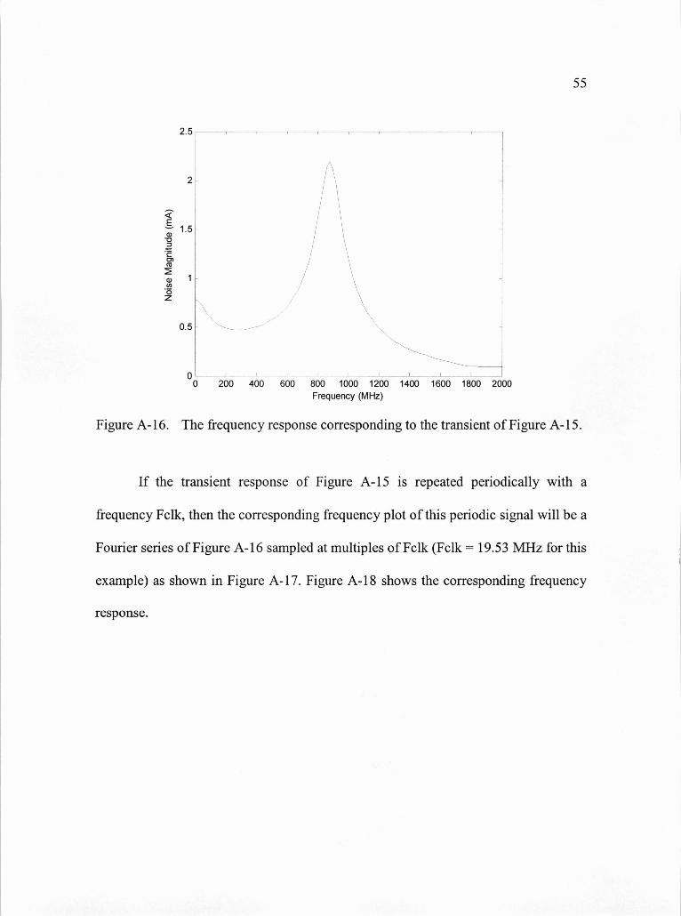
2.5
CCU
)
C,,
0z
0.5
0 200 400 600 800 1000 1200 1400 1600 1800 2000
Frequency (MHz)
55
Figure A-b. The frequency response corresponding to the transient of Figure A-iS.
If the transient response of Figure A- 15 is repeated periodically with a
frequency Fclk, then the corresponding frequency plot of this periodic signal will be a
Fourier series of Figure A-16 sampled at multiples of Fclk (Fclk = 19.53 MHz for this
example) as shown in Figure A-17. Figure A-18 shows the corresponding frequency
response.

5
4
3
a)
E 1C)Ca
a)C,)
0z
31
-2
___.._i_____ UI _____________
0 0.1 0.2 0.3 0.4 0.5 0.6 0.7 0.8
Time (us)
Figure A-17. Noise response of Figure A-15 repeated periodically with a frequencyFclk.
10
9
8
7
J0 200 400 600 800 1000 1200 1400 1600 1800 2000
Frequency (MHz)
Figure A-18. The corresponding frequency spectrum of the transient waveform offigure A-17.
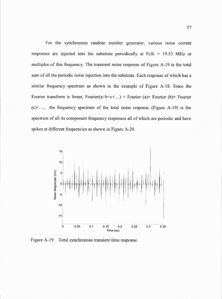
57
For the synchronous random number generator, various noise current
responses are injected into the substrate periodically at Fclk = 19.53 MHz or
multiples of this frequency. The transient noise response of Figure A- 19 is the total
sum of all the periodic noise injection into the substrate. Each response of which has a
similar frequency spectrum as shown in the example of Figure A-18. Since the
Fourier transform is linear, Fourier(a+b+c+...) = Fourier (a)+ Fourier (b)+ Fourier
(c)+..., the frequency spectrum of the total noise response (Figure A- 19) is the
spectrum of all its component frequency responses all of which are periodic and have
spikes at different frequencies as shown in Figure A-20.
15
10
5
LE
:fth
-10
-15
0 0.05 0.1 0.15 0.2 0.25 0.3 0.35
Time (us)
Figure A- 19. Total synchronous transient time response.

-20
-40
-60
s -80
-t3:3
3-100
-120
-140
-1600 50 100 150 200 250 300 350 400
Frequency (MHz)
Figure A-20. The total noise spectrum in decibels

59
6.2. Shape of asynchronous logic noise spectrum Asynchronous Logic
-50 r
-60
-70
-80
-90
1)
-D
-110
-120
-130
-140
-1500 20 40 60 80 100 120 140 160 180 200
Frequency (MHz)
Figure A-2 1. The asynchronous noise spectrum in dB.
The noise of the asynchronous circuit is not the sum of short period signals.
The noise injected into the substrate does not have the typical form of switching noise
from combinational gates and has a white (flat) noise spectrum.
7. Comparison of simulation and measurement results
The synchronous and asynchronous random number generator results are
compared for the two types of substrates, i.e., heavily doped and lightly doped.
7.1. Heavily doped substrates
7.1.1. The synchronous logic circuits
Figure A-22 and Figure A-23 show the results of simulating and measuring
the synchronous circuit noise respectively.

-20
-40
-60
9. -805,
-100
-120
-140
-1600
Simulated Losco CBL Circuit
50 100 150 200 250 300 350 400Frequency (MHZ)
Figure A-22. The simulated noise spectrum of the synchronous random numbergenerator in a heavily doped substrate.
-20
-40
-60
2. -80a,
-100
-120
Measured Losco CBL Circuit
-140
-160-0 50 100 150 200 250 300 350 400
Frequency (MHZ)
Figure A-23. The measured noise spectrum of the synchronous random numbergenerator in a heavily doped substrate. These measurements are beingredone to verify additional frequency components.

61
The synchronous circuit runs at a clock frequency of 10 MHz. In simulation,
spikes are present at the clock frequency and half the clock frequency (5 MHz). In the
measured data, noise spikes are also present at 2.5 MHz. The measured noise spikes
are 7 dB higher than the simulated noise. The RMS noise from measurement is 84.5
mV, the RMS noise from simulation is 50.16 mV. The noise floor from measurement
is at -84 dB, the noise floor from simulation is -78 dB.
7.1.2. The asynchronous logic circuits
Figure A-24 and Figure A-25 show the results of simulating and measuring
the asynchronous random number generator circuit noise respectively.
-20
-40
-60
V;-80
C(5
-100
-120
-140
Losco NCL Simulation
0 50 100 150 200 250 300
Frequency (MHz)
Figure A-24. The simulated noise spectrum of the asynchronous random numbergenerator in a heavily doped substrate. The simulation frequency canbe improved and it is expected that the skirts around the three peakswould be significantly reduced.

62
-20
-40-
-60
w -80
-100
-120
-140
Losco NCL Measurement
0 50 100 150 200 250 300Frequency (MHz)
Figure A-25. The measured noise spectrum of the asynchronous random numbergenerator in a heavily doped substrate.
It takes the data signal in the asynchronous circuit approximately 30 ns to
complete a single loop through the multiplier, the adder, and the register as described
in Section 4.1. The measured asynchronous noise is white except for a spike at 33.3
MHz, which corresponds to a period of 30 ns. The asynchronous noise found by
simulation has a spike at 33.33 MHz and the harmonics 66.6 MHz, 133.3 MHz and
199.9 MHz. The RMS noise from measurement is 12.4804 mV, the RMS noise from
simulation is 23.23 mV. The noise floor from measurement is -81 dB, the noise floor
from simulation is -79 dB.
7.2. Lightly doped substrates
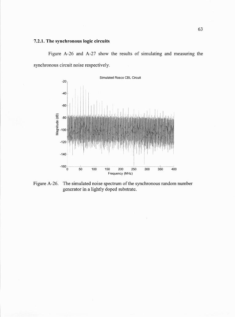
63
7.2.1. The synchronous logic circuits
Figure A-26 and A-27 show the results of simulating and measuring the
synchronous circuit noise respectively.
-20
-40
-60
-80a)
-100
-120
-140
-1600
Simulated Rosco CBL Circuit
50 100 150 200 250 300 350 400Frequency (MHZ)
Figure A-26. The simulated noise spectrum of the synchronous random numbergenerator in a lightly doped substrate.

-20
-40
-60
-100
-120
-140
Measured Rosco CBL Circuit
-1600 50 100 150 200 250 300 350 400
Frequency (MHz)
Figure A-27. The measured noise spectrum of the synchronous random numbergenerator in a lightly doped substrate.
The synchronous circuit runs at a clock frequency of 10 MHz, and spikes are
present in the spectrum at harmonics of that frequency. The measured noise spikes are
8 dB higher than the simulated noise. The RMS noise from measurement is 132 mV,
the RMS noise from simulation is 1033 mV. The noise floor from measurement is at
-70 dB, the noise floor from simulation is -74 dB.
7.2.2. The asynchronous logic circuits
Figure A-28 and Figure A-29 show the results of simulating and measuring
the asynchronous circuit noise.

E-o
, -800:3
0)(3,
-100
-120
140
Rosco NCL Simulation
0 50 100 150 200 250 300Frequency (MHz)
65
Figure A-28. The simulated noise spectrum of the asynchronous random numbergenerator in a lightly doped substrate. The simulation accuracy can beimproved. With improvements, it is expected that the skirts around thepeak frequencies would be significantly reduced.
-D
0)(3,
-20
-40
-60
-80
-100
-120
Rosco NCL Measurement
-140
- ----- _j___ I
0 50 100 150 200 250 300Frequency (MHZ)
Figure A-29. The measured noise spectrum of the asynchronous random numbergenerator in a lightly doped substrate.

As in the heavily doped substrate, it takes the data signal approximately 30 ns
to complete a single ioop through the multiplier, the adder, and the register as
described in Section 4.1. The measured asynchronous noise is white except for a
spike at 33.3 MHz, which corresponds to a period of 30 ns. The asynchronous noise
found by simulation has a spike at 33.33 MHz and the harmonics 66.6 MHz, 133.3
MHz and 199.9 MHz. The RMS noise from measurement is 11.73 mV, the RMS
noise from simulation is 73.18 mV. The noise floor from measurement is -80 dB, the
noise floor from simulation is -74 dB. The higher noise floor in simulation accounts
for the higher RIVIS noise value.
7.3. Comparison of results
Table A-i summarizes the measurement and simulation results of Section 7. It
is obvious that the synchronous circuits out perform the asynchronous circuit in terms
of circuit size and operating speed. The asynchronous circuits are nearly four times
larger than the synchronous circuits. The synchronous circuits were also designed to
run at clock frequencies of up to 100 MHz, while the asynchronous circuits can only
run at a fixed internal frequency of 33.33 MHz, which is the time it takes a data signal
to pass through one ioop of the signal path. The asynchronous circuits, however,
inject less noise into the substrate. Comparing the RMS noise measured at the sensor
amplifier output it is observed that the synchronous circuits inject 84.5 mV and 132
mV of noise into the heavily doped and lightly doped substrates respectively, while
the asynchronous circuits inject 12.48 mV and 11.73 mV respectively. The

67
synchronous circuit injects approximately 6.7 and 11 times more noise than the
asynchronous circuit in the heavily doped and lightly doped substrates respectively.
Table A-i Summary of the measurement and simulation results for the randomnumber generator circuits.
RMS Noise FundamentalCircuit noise floor frequency spike
(mY) (dB) (MHz)
Synchronous Measurement 84.5 -84 2.5Heavily Simulation 50.16 -78 5doped Asynchronous Measurement 12.48 -81 33.33
Simulation 23.23 -79 33.33
Synchronous Measurement 132 -70 10Lightly Simulation 103.7 -74 10doped Asynchronous Measurement 11.73 -80 33.3
Simulation 73.18 -74 33.3
The synchronous circuits are driven by a clock at 10 MHz, this causes the
gates within the circuits to switch at fixed frequencies that are multiples of the clock
frequency. This, in turn, causes the spikes that are observed in the power spectrums of
the synchronous circuits. The asynchronous power spectrums, on the other hand, are
white except for the spike at 33.3 MHz that corresponds to a whole cycle through the
circuit.