hvsw-03 high voltage high repetition rate pockels cell
TRANSCRIPT
rev 1.16 / 2021 05 24
HVSW-03
high voltage high repetition rate
Pockels cell driver
with embedded power supply
User manual
Warning! This equipment produces high voltages that can be very dangerous. Please read
user manual before starting operations.
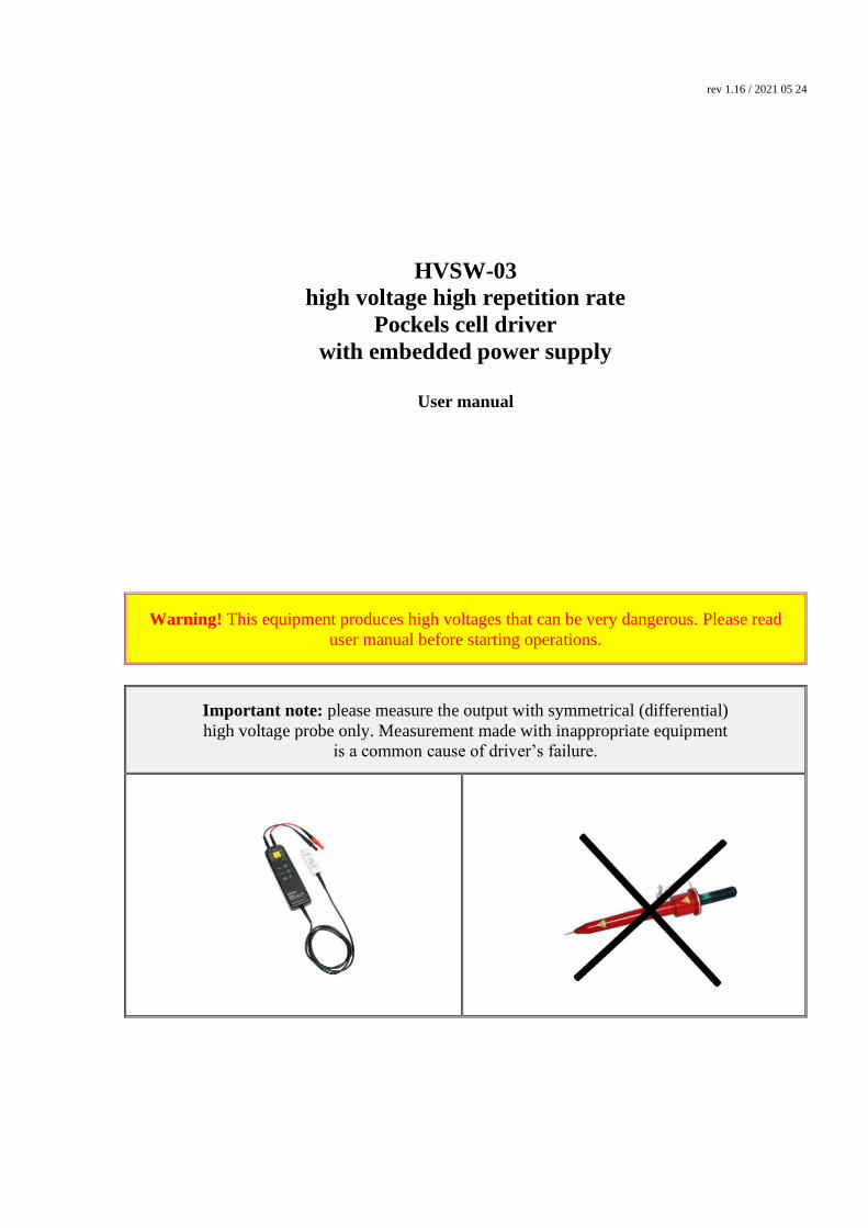
Important note: please measure the output with symmetrical (differential)
high voltage probe only. Measurement made with inappropriate equipment
is a common cause of driver’s failure.

Table of content
Table of content ............................................................................................................................... 2
Description ........................................................................................................................................ 3
Connectors, pins, interface signals ..................................................................................................... 4
Safety ................................................................................................................................................ 6
Operations (analogue interface) ........................................................................................................ 7
RS-485 interface description .............................................................................................................. 7
Software description ......................................................................................................................... 8
Technical notes ............................................................................................................................... 10
Specifications ................................................................................................................................. 11
Dimensions ..................................................................................................................................... 12
Performance, output oscillograms ................................................................................................... 13
Appendix A. RS-485 communicative protocol ................................................................................... 14

Description
HVSW-03 is a specialized Pockels cell driver that performance is optimized for pico- and
femtosecond lasers. Main applications are pulse picking and regenerative amplifier control.
Maximal output voltage is 2kV; maximal repetition rate achieves 1MHz at 1.5kV output voltage.
Modification with performance of 2MHz at <1.0kV output voltage is available on request.
Transition times are as fast as 5-7ns in dependence on load capacitance and driver’s
configuration (see also Software description section). Pulse width is <15ns (fixed), then 100-
2000ns (adjustable by the customer), see also Software description section.
Interfaces are analogue and RS-485. Configuration software for Windows® 7 is available.
Compact design (about 0.3dm3), conductive cooling through the bottom surface and embedded
high voltage power supply (i.e. driver’s input is +24V DC) are additional benefits.

Connectors, pins, interface signals
INTERFACE (D-SUB mixed contact connector FM11W1):
PIN (color) DESIGNATION DESCRIPTION
1 (yellow) HV Program
Analogue voltage applied to this pin defines
the amplitude of high voltage pulses at
driver's output.
0V on this pin corresponds to 0V at the
output. 2V on this pin corresponds to 2kV
at the output (calibration 1:1000).
2, 10 (black) GND (analogue
interface, RS-485)
Return of Interface signals (HV Program,
HV Enable, Pulse, Gate Limit Fault,
Overtemp Fault).
Grounding of RS-485 interface to be used in
the case of high level of EMI affecting
quality of RS-485 connection and the need to
equalize the potentials of receiver and
transmitter.
3 (black, thick
wire) +24V DC Return +24V DC power supply negative
4 (red) Overtemp Fault
In the case of overheating driver sets up the
fault on this pin (TTL high – fault, low – no
fault) and stops the operations till fault reason is eliminated and driver is rebooted
(disabled and enabled again).
5 (blue) HV Enable
+5V applied to this pin turns on embedded
high voltage power supply and enables the
output.
This pin is also used to reboot the driver in
the case of overheating and other faults. To
remove overtemp fault state driver should
be disabled and enabled again.
6 (orange) Gate limit Fault
Gate limit is a hardware protection of laser
optics from too long pulses applied to the
Pockels cell controlling the regenerative
amplifier.
If pulse width applied to Pulse pin (A1)
exceeds Gate limit value driver forcibly
cuts off the pulse and sets up the Gate limit
Fault (TTL high – fault, low – no fault).
Despite the Fault state driver continues the
operations. To remove state driver should
be disabled and enabled again.
7 (violet) RS-485 “+” RS-485 «+» to be applied here
8 (green) RS-485 “–” RS-485 «–» to be applied here
9 (red, thick wire) +24V DC +24V DC power supply positive.
Rated current – 5.5A max.
A1 (black) Pulse
In Fixed pulse width mode (see also
Software description section):
TTL signal applied to this pin initiates HV
pulse at driver’s output. Rising edge
triggered. Trigger level is 3V. HV pulse
width is fixed and <15ns.
In Variable pulse width mode (see also
Software description section):
Driver’s output repeats TTL signal
applied to this pin. Minimal pulse width is
100ns, maximal pulse width is 2000ns or
Gate limit (what’s less). Minimal inter-
pulse interval is 100ns.
Input impedance is 50Ohm.
Signal amplitude delivered to the switch
should be +5V DC assuming divider of
switch’s input impedance and pulse
generator output impedance.
HV OUTPUT (flying leads):
Two wires, each of 70mm length
Other wire’s length and termination are available on request. Shielded output wires
reducing EMI, but slightly decreasing the performance are available on request.
LEDs:
POWER (green) – LED lits steadily while device is powered.
RS485 (red) – LED is lit steady when device is in stand-alone mode (analog interface is
enabled), and blinks when device is being controlled via RS-485. In bootloader (update) mode
this LED makes double blinks.
STATE (blue) – LED blinks slowly when device is in stand-by mode; it blinks fast when error
(overheat) is detected; and it is lit steady when HV output is enabled.
MOUNTING AND GROUNDING:
Driver to be mounted with 3pcs M4 screws (recommended screws are DIN 912, M4x10
or longer).
Grounding policy
Interface signals and interface return are insulated from +24VDC, HV output and coverage
case. +24VDC positive and negative are insulated from Interface, HV output and coverage
case. HV output electrical potentials are switched relatively potential of the coverage case.
Neither HV output positive nor HV output negative can be grounded in any way. Grounding
of HV output e.g. while measuring the output with oscilloscope is a common reason of
driver’s failure.
Other grounding policies are available on request.
COOLING:
Driver is conductively cooled through the bottom surface, which in dependence on actual
heat dissipation should be attached either to massive chassis, or to heat sink or to cold
plate of the appropriate performance.
For better heat removal thermal grease or equivalent may be used.
Safety
Warning! This equipment produces high voltages that can be very dangerous. Don’t be
careless around the equipment.
Assemble the entire setup before powering the device.
• Avoid casual contacts of personnel with output cables and with the load
• Do not connect / disconnect output cables while driver is turned on
• Do not operate with disconnected load
• Do not turn the driver on if it was already damaged with water, chemicals, mechanical or
electrical shock
• Do not self-repair the driver, there are no user-serviceable parts inside
• Driver’s input-to-output insulation isn’t a safety feature, but just functional one, so we
highly recommend to use low voltage power supply with input-to-output insulation
providing appropriate level of protection (4000VAC or 2500VAC in dependence on your
application)

Operations (analogue interface)
[Pre-configuration, optional]
1. Connect +24V DC power supply to the driver, connect driver to PC (or to
another controlling device)
2. Run provided Windows® software (or terminal software)
3. Configure the driver using provided Windows® software (or using RS-
485 commands)
4. Disconnect the driver from PC (from another controlling device)
[Operations]
1. Attach driver to the cool plate (another cooling device)
2. Connect +24V DC power supply, Pockels cell and pulse generator to the
driver. Do not apply +24V DC power before the entire setup is
completely assembled
3. Turn on +24V DC power supply to power up the driver
4. Apply HV Program (pin 1) analogue voltage corresponding to the desired
output voltage
5. Enable the driver using HV Enable signal (pin 5)
6. Apply Pulse signal (pin A1) with the desired pulse width and repetition
rate
Important note: that’s impossible to command the driver via RS-485 interface and via
analogue interface at the same time. Once RS-485 connection is established, driver ignores
signals applied to the analogue interface.
To switch driver from RS-485 interface to the analogue interface (or vice versa),
power should be removed from the driver and then applied again.
RS-485 interface description
RS-485 connection parameters: 57600 bps, 8 data bits, 1 stop bit, no parity.
Default protocol is described in Appendix A.
Simplified protocols are available on request.
Software description
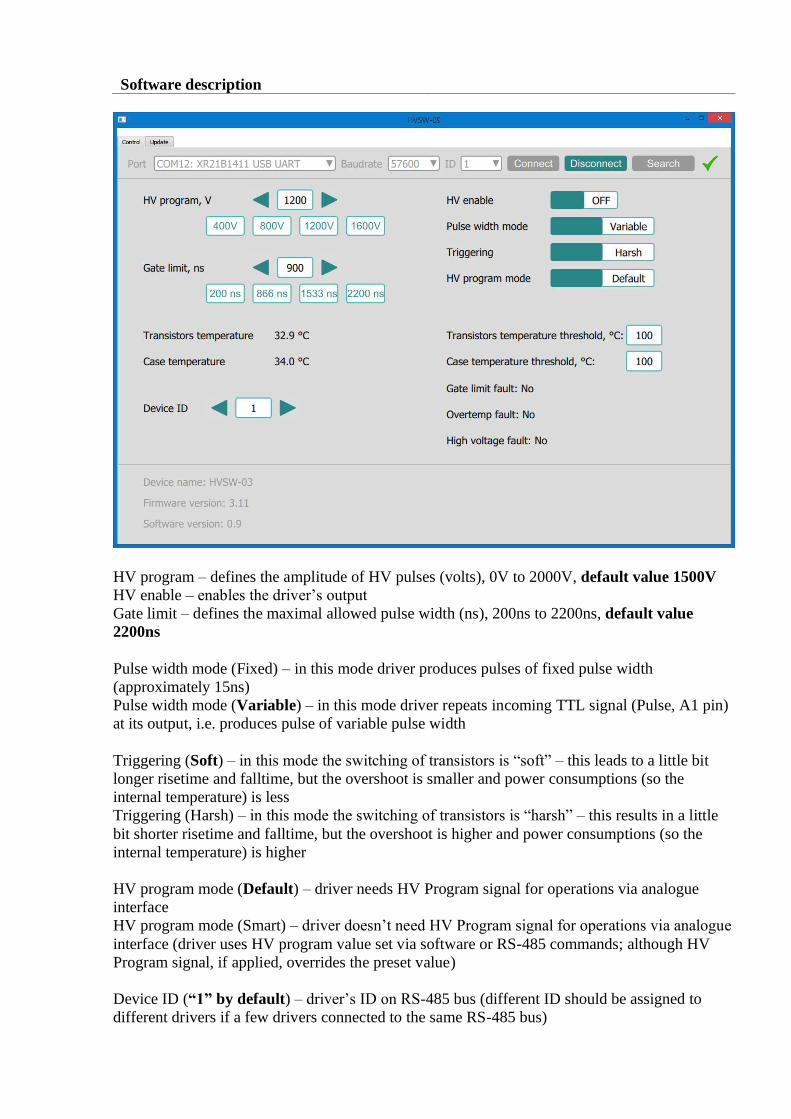
HV program – defines the amplitude of HV pulses (volts), 0V to 2000V, default value 1500V
HV enable – enables the driver’s output
Gate limit – defines the maximal allowed pulse width (ns), 200ns to 2200ns, default value
2200ns
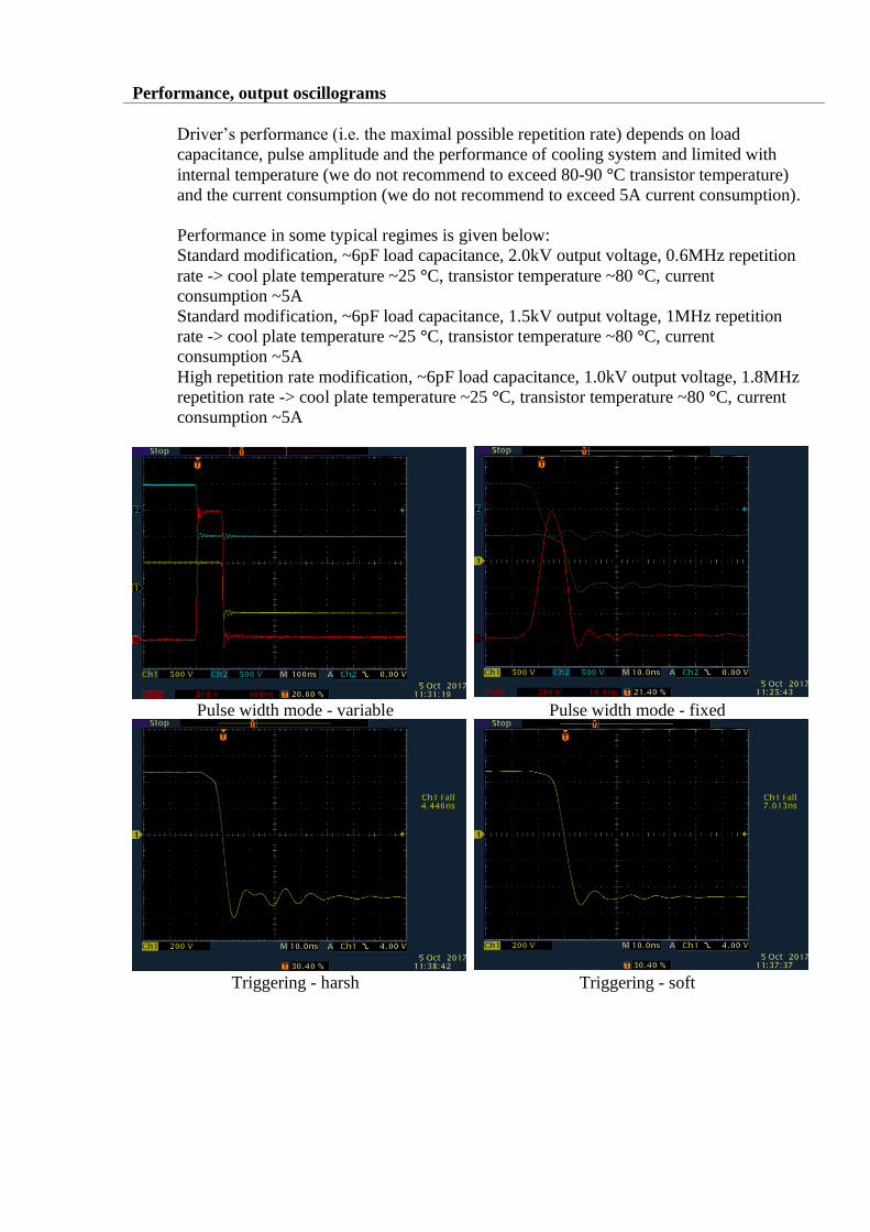
Pulse width mode (Fixed) – in this mode driver produces pulses of fixed pulse width
(approximately 15ns)
Pulse width mode (Variable) – in this mode driver repeats incoming TTL signal (Pulse, A1 pin)
at its output, i.e. produces pulse of variable pulse width
Triggering (Soft) – in this mode the switching of transistors is “soft” – this leads to a little bit
longer risetime and falltime, but the overshoot is smaller and power consumptions (so the
internal temperature) is less
Triggering (Harsh) – in this mode the switching of transistors is “harsh” – this results in a little
bit shorter risetime and falltime, but the overshoot is higher and power consumptions (so the
internal temperature) is higher
HV program mode (Default) – driver needs HV Program signal for operations via analogue
interface
HV program mode (Smart) – driver doesn’t need HV Program signal for operations via analogue
interface (driver uses HV program value set via software or RS-485 commands; although HV
Program signal, if applied, overrides the preset value)
Device ID (“1” by default) – driver’s ID on RS-485 bus (different ID should be assigned to
different drivers if a few drivers connected to the same RS-485 bus)

Transistor temperature threshold – maximal value 100 °C, default value 100 °C
Case temperature threshold – maximal value 100 °C, default value 70 °C

Technical notes
• Performance of the module greatly depends on load capacitance. Full
performance is achievable at load capacitance typical to Pockels cells used in
laser industry (5-7pF).
Higher load capacitance decreases maximal allowed repetition rate
• Module’s output is bipolar. This means that e.g. 2kV pulse is physically formed
by applying +1kV to one output wire
and -1kV to another (see figure)
Nevertheless, all descriptions of HV output are given in terms of voltage
differences. Please keep this in mind!
• Sequential pulses have reversed polarity. Since driver is built on full bridge
schema, each of two output wires varies its potential between +V and –V values
(blue and yellow curves below). As a result, the voltage difference between two
wires can be both positive and negative (red curve on the picture below).
• Arbitrary (random) signal applied to Pulse pin may damage the driver.
Please ensure Pulse signal follows the next rules:
- Minimal allowed pulse width is 100ns
- Maximal allowed pulse width is 2000ns
- Minimal allowed distance between pulses is 100ns
- Maximal allowed distance between pulses - no limitation
- Maximal allowed repetition rate is 1MHz for standard drivers and 2MHz for
high repetition rate modification.
Not every point above has the corresponding hardware protection. Please ensure
the applied signals are within the allowed ranges.

Specifications
ELECTRICAL SPECIFICATION
Input +24V DC; 5.5A max
Output
Pulses of high voltage and high repetition rate
delivered to the capacitive load (e.g. to the Pockels
cell)
Output type Bipolar (see also Technical notes section)
Pulse basement 1 0V, fixed
Pulse amplitude 1, 2 adjustable in 0-2kV range
Maximal repetition rate 2 Up to 1-2MHz (see also How to order section)
Minimal repetition rate
Single shot (there is an internal restriking circuit
which makes the operations at such a low repetition
rate possible)
Pulse width
Fixed, about 15ns in Fixed pulse width mode (see
also Software description section)
100ns-2000ns adjustable (other on request) in
Variable pulse width mode (see also Software
description section)
Interpulse interval >100ns
Risetime/falltime 3 5-7ns
Delay time <50ns
Jitter <0.5ns (±250ps)
Load capacitance 5-7pF typically
Protections - From too long pulses (Gate limit), adjusted by the
customer in 200ns to 2200ns range 3
- From overheating
Environment
Operation temperature +10...+40 °C
Storage temperature -20...+60 °C
Humidity 90%, non-condensing 1 In terms of bipolar output (see also Technical notes section)
2 Maximal pulse repetition rate depends on pulse amplitude, pulse amplitude and pulse
repetition rate cannot achieve their maximums at the same time 3 10-90% level, warranted at load capacitance 11pF and below 4 These and other parameters might be changed upon request
MECHANICAL SPECIFICATION
Size (LxWxH) 169x60x32mm
Weight <0,5kg

Dimensions
How to order?
At the moment there are two modifications different with maximal repetition rate and
risetime/falltime:
Modification Maximal repetition rate Risetime/falltime
HVSW-03 (standard
modification)
1MHz (can be damaged if
operated at higher repetition rate)
5-7ns
HVSW-03-HF (high
repetition rate modification)
2MHz (can be damaged if
operated at higher repetition rate)
6-8ns (approx. 1ns slower than
in standard modification)
Performance, output oscillograms
Driver’s performance (i.e. the maximal possible repetition rate) depends on load
capacitance, pulse amplitude and the performance of cooling system and limited with
internal temperature (we do not recommend to exceed 80-90 °C transistor temperature)
and the current consumption (we do not recommend to exceed 5A current consumption).
Performance in some typical regimes is given below:
Standard modification, ~6pF load capacitance, 2.0kV output voltage, 0.6MHz repetition
rate -> cool plate temperature ~25 °C, transistor temperature ~80 °C, current
consumption ~5A
Standard modification, ~6pF load capacitance, 1.5kV output voltage, 1MHz repetition
rate -> cool plate temperature ~25 °C, transistor temperature ~80 °C, current
consumption ~5A
High repetition rate modification, ~6pF load capacitance, 1.0kV output voltage, 1.8MHz
repetition rate -> cool plate temperature ~25 °C, transistor temperature ~80 °C, current
consumption ~5A
Pulse width mode - variable Pulse width mode - fixed
Triggering - harsh Triggering - soft

Appendix A. RS-485 communicative protocol
The present section describes RS-485, binary, master-slave protocol. Only one active master (at
the same time) can be connected to the bus, and one or several (up to 254) slave nodes can be
connected to the same bus. HVSW-03 is a slave device and responds to the transactions initiated
by the master. Each slave device has an unique address between 1 and 254 decimal and also
recognizes the broadcast address 0. Available bus baudrates for device are: 4800, 9600, 19200,
38400, 57600 (default), 115200. Available baudrate for bootloader: 57600.
Data packet format from the master:
Byte Description
0 Synchronization/flags. 1 byte in format:
1 0 1 0 S W R M
M: Master bit (1 – packet is sent by the master, 0 – by slave)
R: Retransmit bit (1 – Retransmitted packet, 0 – Normal packet)
W: Write bit (1 – request sends data, 0 – request asks data)
S: Sequel bit (0 – last/only packet, 1 – indicates that a further packet(s)
are to be expected
1 Length of the data field. 1 byte (0 - no data; 1… 255 – data length)
2 Device ID. 1 byte (1..254, 0 indicates broadcast transmission)
3 Parameter (or Function)
0x00 … 0x3F: common parameters
0x40 … 0xFF: device specific parameters
4 Data field (optional). 0..255 bytes, least significant byte first.
Transmitting more than 255 bytes is possible by splitting up the data
field in a sequence of packet transmissions by the use of the S Bit of the
synchronization and flags byte.
4+Length CRC8 ITU-T (polynomial x8+x2+x+1 / 0x07) over all bytes
A slave uses the frame format described below with the same synchronization and flag byte as
the master.
Byte Description
0 Synchronization/flags:
1 0 1 0 S W R M (see flags description in master section)
1 Length of the data field. 1 byte (0 - no data; 1… 255 – data length)
2 Result, 1 byte:
0x00 ≡ no error
0x01 … 0x7F ≡ common errors
0x80 … 0xFF ≡ device specific errors
Common errors:
0x01 Parameter/Function not available
0x02 Parameter is read only
0x03 Request packet has an invalid amount of data
0x04 Value transmitted in the request packet is out of range
0x05 Current request cannot be processed at the moment
3 Data field (optional). 0..255 bytes, least significant byte first
3+Length CRC8 ITU-T (polynomial x8+x2+x+1 / 0x07) over all bytes
A slave responds message in less than 50ms after receiving a fully initiating a transaction from a
master. Master must generate a time out at least 100ms after finishing a transaction.
Common parameters / functions

0x00: Ping (read only), data length: 0 byte. A slave answers by sending a packet with no data.
0x01: Device ID (write only), data length: 1 byte, range: 1..254, default value: 1. Function sets
the new device ID, which is used immediately after this write request.
0x02: Protocol version (read only), data length: 1 byte, range: 1..254. A slave returns value 1.
0x03: Device part number (read/write), data length: 2 bytes, range: 0..65535. Function
sets/returns device part number.
0x04: Device serial number (read/write), data length: 2 bytes, range: 0..65535. Function
sets/returns device serial number.
0x05: Hardware version (read/write), data length: 2 bytes, range: 0..65535. Function
sets/returns device hardware version.
0x06: Software version (read only), data length: 2 bytes, range: 0..65535. Function returns
device software version.
0x07: Device string (read only), data length: arbitrary, ASCII string. Function returns device
name or description.
0x08: Bootloader control and status (read or write), data length: 1 byte, data format: bit field.
Function controls the bootloader using the following format:
Write request:
Bit 0: Activate bootloader
Bit 1: Clear memory
Bit 2: Boot application
Read request:
Bit 0: Bootloader running (1 – yes, 0 – no)
Bit 1: Memory cleared (1 – yes, 0 – no)
Bit 2: Valid application in memory (1 – yes, 0 – no)
0x09: Bootloader Stream (write only), data length: N packets of 1..255 bytes.
0x0A: Device status (read only), data length: 2 bytes, data format: bit field. Function returns
device status in the following format:
Bit 0: At least one warning is present
Bit 1: At least one error is present
Bit 3: Bootloader is active
Bit 4: Device is ready
Bit 7: Device is “On”
0x0B: Available bus speed (read only), data length: 2 bytes, data format: bit field. Indicates
availability of device specific bus speed implementations (in Bit/s)
Bit 0: 4.800
Bit 1: 9.600
Bit 2: 19.200
Bit 3: 38.400
Bit 4: 57.600
Bit 5: 115.200
Bits 6..15: reserved
0x0C: Set bus speed (write only), data length: 2 bytes, data format: bit field. Function sets bus
speed.
Bit 0: 4.800
Bit 1: 9.600
Bit 2: 19.200
Bit 3: 38.400
Bit 4: 57.600 (Default Setting)
Bit 5: 115.200
Bits 6..15: reserved
0x0D: Bus mute (read/write), data length: 1 byte, data range: 0-1 (0 = communication is on, 1 =
communication is off). Switches off the serial communication of a device until it is switched on

again using this parameter. After power on (supply voltage) device has its serial communication
switched ON.
Device specific parameters / functions
0x40: High voltage (read/write), data length: 2 bytes, range: 0..2000. Sets or gets high voltage in
volts.
0x41: Gate Limit (read/write), data length: 2 bytes, range: 200..2200. Sets or gets gate limit in
nanoseconds.
0x42: Transistors temperature threshold (read/write), data length: 2 bytes, range: 0..1600.
Sets or gets transistors temperature threshold in 0.1 °C (e.g. 800 corresponds to 80.0 °C)
0x43: Case temperature threshold (read/write), data length: 2 bytes, range: 0..1600. Sets or
gets case temperature threshold in 0.1 °C (e.g. 800 corresponds to 80.0 °C)
0x44: HV enable (read/write), data length: 1 byte, range: 0 .. 1. Enables (1) or disables (0) high
voltage.
0x45: Pulse width mode (read/write), data length: 1 byte, range: 0..1. Sets or gets pulse width
mode (1 – fixed, 0 – variable).
0x46: Triggering mode (read/write), data length: 1 byte, range: 0..1. Sets or gets triggering
mode (1 – soft, 0 – harsh).
0x47: HV Program mode (read/write), data length: 1 byte, range: 0..1. Sets or gets HV program
mode (1 – smart, 0 – default).
0x60: Get sensors (read only), data length: 1 byte, range: 0..255. Returns device sensors in the
following format:
Bit 0: Overtemperature error
Bit 1: Gate limit error
Bits 2-5,7: reserved
Bit 6: HV fault error
0x61: Get transistors temperature (read only), data length: 2 bytes, range: 0..1600. Returns
current transistors temperature in 0.1 °C (e.g. 800 corresponds to 80.0 °C).
0x62: Get case temperature (read only), data length: 2 bytes, range: 0..1600. Returns current
case temperature in 0.1 °C (e.g. 800 corresponds to 80.0 °C).
0xF2: Get all monitors (read only), data length: 5 bytes. Returns all monitors in the following
format: sensors (1 byte), transistors temperature (2 bytes), case temperature (2 bytes).
0xF1: Get all parameters (read only), data length: 13 bytes. Returns all parameters in the
following format: high voltage (2 bytes), gate limit (2 bytes), transistors temperature threshold
(2 bytes), case temperature threshold (2 bytes), sensors and states (1 byte in the following
format: Bit 0: overtemperature error, Bit 1: gate limit error, Bit 2: high voltage enable state, Bit
4: pulse width mode state, Bit 5: triggering mode state, Bit 6: HV fault error), transistors
temperature (2 bytes), case temperature (2 bytes).
Examples:
A1 00 01 00 FC – ping device with ID = 1 (answer: A0 00 00 48)
A1 00 01 61 DC – get transistors temperature for device with ID = 1 (answer: A0 02 00 EF 00
5F – temperature is 23.9 °C)
A5 02 01 40 E8 03 EC - set high voltage to be 1000V for device with ID = 1 (no answer)