hx8227-a01 - i-lcd.com doc no. hx8227-a-ds ) hx8227-a01 720ch tft lcd source driver with built-in...
TRANSCRIPT

( DOC No. HX8227-A-DS )
HX8227-A01 720CH TFT LCD Source Driver with Built-in TCON Preliminary version 04, March 2006

-P.1- Himax Confidential
March 2006 This information contained herein is the exclusive property of Himax and shell not be distributed, reproduced, or disclosed in whole or in part without prior written permission of Himax. Subject to change without notice.
1. General Description
HX8227-A is a 720-channel output source driver with built-in TCON (Timing Controller). The source driver receives 24-bit digital display data with single clock edge and generates corresponding 256 level gray scale voltage outputs to realize 16M colors display. Positive and negative polarity voltages can be alternately output from each channel in line (row) inversion or frame inversion driving methods.
2. Features
Source Driver 720 channels output source driver for TFT LCD panel Support 8-bit data input for 256 level gray scales Dynamic range: AVSS+0.2V ~ AVDD-0.2V Output voltage deviation: +20mV. Driver power supply voltage (AVDD): 4.8 ~ 5.2V Bare chip with gold bumper for COG solution.
Embedded Timing Controller Support 480 RGBx272, 480RGBx240, 240RGBx320, and 240RGBx240 resolutions Supporting 24-bit (8 bits x 3) parallel RGB and 8-bit serial RGB input interfaces Operation frequency: 15 MHz max in parallel RGB interface. 33MHz max in serial RGB interface. Support PAL decimation in 480RGBx240 or 240RGBx240 resolutions. Selectable line (row) inversion and frame inversion driving schemes. Provide the control timing of the source driver and the gate driver. Logic power supply voltage (DVDD): 2.25V ~ 3.6V
HX8227-A01 720CH TFT LCD Source Driver with Built-in TCON Preliminary Version 04 March 2006

-P.2- Himax Confidential
March 2006 This information contained herein is the exclusive property of Himax and shall not be distributed, reproduced, or disclosed in whole or in part without prior written permission of Himax. Subject to change without notice.
HX8227-A01 720CH TFT LCD Source Driver with Built-in TCON
DATA SHEET Preliminary V04
3. Block Diagram
Output BufferAVDDAVSS
DVSSDVDD
Gammaresistorstrings
V0 ~ V13
Timing Controller
LRDISPCLK
240-bit Bidirectional Shift Register
PO
L
OEH
D27
~D20
D17
~D10
D07
~D00
RES
ETB
LFNB
W
HS
VS
CKV
STV
OEV
CO
MS
IGD
ISPG
D/AConverter
S1
S2
S3
S71
8
S71
9
S72
0
720 Channel Sample and Hold Circuit
24-b
it D
ata
LR PS
RE
S2,1
MS
DE
Figure 3. 1 Block diagram

-P.3- Himax Confidential
March 2006 This information contained herein is the exclusive property of Himax and shall not be distributed, reproduced, or disclosed in whole or in part without prior written permission of Himax. Subject to change without notice.
HX8227-A01 720CH TFT LCD Source Driver with Built-in TCON
DATA SHEET Preliminary V04
4. PAD Location (IC Face View)
No.989
No.981
TEST_IO4
TEST_IO3
No.1
DUMMY(* )DUMMY(* )DUMMY(* )
DUMMY(*)
BUMP SIZE
TEST_IO2
TEST_IO1
Y-AMP through pln
No. 245
No.254
0
+x
+y
20 µm 10 µm
20µ
m10
µm
100 µm
30µ
m30
µm3
0µm
20µm
10µm
20µ m10µm
100
µm
30 µm30 µm30µ m
Remark:DUMMY(*) are used to measure to contact resistance
50 µm( x)X100µ m(y)36 µm( x)X120µ m(y)24 µm( x)X100µ m(y)100 µm (x)X50 µm( y)
DUMMYDUMMYDUMMYDUMMYS720S719
OE
(2)C
KV
_R(2)
STV
_R(2)
CO
MSIG
_R(2)
DISPG
AVSS( 6)
AVDD( 6)
DVDD( 1)
MS( 3)DVSS( 1)
RESETB( 3)
DE( 3)
VS( 3)
HS( 3)
DISP( 3)
CLK( 3)
DVSS(1)R/L( 3)
DVDD( 1)
DVSS( 1)TEST I/O( 3)
TEST I/O( 3)
D26( 3)
D27( 3)
D25( 3)
D24( 3)
D23( 3)
D22( 3)
D21( 3)
D20 (3)DVSS( 1)
TEST I/O( 3)
TEST I/O( 3)
AVDD( 6)
DUMMY( 3)
V13( 3)
V12( 3)
V11( 3)
V10( 3)
V9( 3)
V8( 3)
V7( 3)
DUMMY( 3)
DUMMY( 3)
V6( 3)
V5( 3)
V4( 3)
V3(3)
V2( 3)
V1( 3)
V0( 3)
DUMMY( 3)
AVSS( 6)
D17( 3)
D16( 3)
D15( 3)
D14( 3)
D13( 3)
D12( 3)
D11( 3)
D10( 3)
D7( 3)
D6( 3)
D5( 3)
D4( 3)
D3( 3)
D2( 3)
D1( 3)
D0( 3)
DVDD(10 )
DVSS(10 )
TEST 3(3)
TEST2( 3)
TEST1( 3)
AVSS( 6)
AVDD( 6)
LFNBWRES2
OE
(2)
CKV
_R(2)
STV
_R(2)
CO
MS
IG_R
(2)
DUMMYDUMMY DUMMYDUMMY S1S2
S3
Y-AMP through pln
Y-AMP through pln
Y-AMP through pln
CLK_TRG( 1)PS( 1)
RES1(1 )
POINT 1
120um
52um22um
22um
100um
24um
36um
52um
A-PAD (Output)
140um
28um52um
100um
24um
(Spacing Is Min. Value)
100um
50um
20um70um
C-PAD (Dummy)
140um
20um
120um
36um
26um
52um
70um
100um
50um20um
Min. Min.
Min.
Min.
B-PAD (Input)
D-PAD
(Spacing Is Min. Value)
Figure 4. 1 Pad location

-P.4- Himax Confidential
March 2006 This information contained herein is the exclusive property of Himax and shall not be distributed, reproduced, or disclosed in whole or in part without prior written permission of Himax. Subject to change without notice.
HX8227-A01 720CH TFT LCD Source Driver with Built-in TCON
DATA SHEET Preliminary V04Chip Information
Size Items Pad name X Y
Unit
Chip size - 19100 1300 Wafer thickness - 400
Output pad (Type A) 24 100 Input pad (Type B) 50 100 Bump size Dummy pad (Type C) 36 120
um
Table 4. 1
Alignment Mark Configuration and Coordinate
(1-a) (x, y) = (-9201.80, -344.00) (1-b) (x, y) = (9201.80, -344.00)
20um 10um
20um
10um
30um
30um
30um
100um
Figure 4. 2 Alignment mark configuration

-P.5- Himax Confidential
March 2006 This information contained herein is the exclusive property of Himax and shall not be distributed, reproduced, or disclosed in whole or in part without prior written permission of Himax. Subject to change without notice.
HX8227-A01 720CH TFT LCD Source Driver with Built-in TCON
DATA SHEET Preliminary V04Pad layout coordinate (Unit: µm)
No. Name X Y BUMP size X Pitch Y Pitch No. Name X Y BUMP size X Pitch Y Pitch1 DUMMY(*) -9422 -427 B -25 -95 51 TEST I/O -5125 -522 B 70 0 2 DUMMY(*) -9447 -522 B 70 0 52 TEST I/O -5055 -522 B 70 0 3 DUMMY(*) -9377 -522 B 70 0 53 TEST I/O -4985 -522 B 80 0 4 DUMMY(*) -9307 -522 B 160 0 54 TEST I/O -4905 -522 B 70 0 5 DISPG -9147 -522 B 70 0 55 TEST I/O -4835 -522 B 70 0 6 DISPG -9077 -522 B 677 0 56 TEST I/O -4765 -522 B 75 0 7 AVSS -8400 -522 B 70 0 57 D27 -4690 -522 B 70 0 8 AVSS -8330 -522 B 70 0 58 D27 -4620 -522 B 70 0 9 AVSS -8260 -522 B 70 0 59 D27 -4550 -522 B 80 0
10 AVSS -8190 -522 B 70 0 60 D26 -4470 -522 B 70 0 11 AVSS -8120 -522 B 70 0 61 D26 -4400 -522 B 70 0 12 AVSS -8050 -522 B 100 0 62 D26 -4330 -522 B 80 0 13 AVDD -7950 -522 B 70 0 63 D25 -4250 -522 B 70 0 14 AVDD -7880 -522 B 70 0 64 D25 -4180 -522 B 70 0 15 AVDD -7810 -522 B 70 0 65 D25 -4110 -522 B 80 0 16 AVDD -7740 -522 B 70 0 66 D24 -4030 -522 B 70 0 17 AVDD -7670 -522 B 70 0 67 D24 -3960 -522 B 70 0 18 AVDD -7600 -522 B 100 0 68 D24 -3890 -522 B 80 0 19 DVDD* -7500 -522 B 80 0 69 D23 -3810 -522 B 70 0 20 MS -7420 -522 B 70 0 70 D23 -3740 -522 B 70 0 21 MS -7350 -522 B 70 0 71 D23 -3670 -522 B 80 0 22 MS -7280 -522 B 70 0 72 D22 -3590 -522 B 70 0 23 DVSS* -7210 -522 B 80 0 73 D22 -3520 -522 B 70 0 24 RESETB -7130 -522 B 70 0 74 D22 -3450 -522 B 80 0 25 RESETB -7060 -522 B 70 0 75 D21 -3370 -522 B 70 0 26 RESETB -6990 -522 B 80 0 76 D21 -3300 -522 B 70 0 27 DE -6910 -522 B 70 0 77 D21 -3230 -522 B 80 0 28 DE -6840 -522 B 70 0 78 D20 -3150 -522 B 70 0 29 DE -6770 -522 B 80 0 79 D20 -3080 -522 B 70 0 30 VSC -6690 -522 B 70 0 80 D20 -3010 -522 B 80 0 31 VSC -6620 -522 B 70 0 81 DVSS -2930 -522 B 85 0 32 VSC -6550 -522 B 80 0 82 TEST I/O -2845 -522 B 70 0 33 HSC -6470 -522 B 70 0 83 TEST I/O -2775 -522 B 70 0 34 HSC -6400 -522 B 70 0 84 TEST I/O -2705 -522 B 80 0 35 HSC -6330 -522 B 80 0 85 TEST I/O -2625 -522 B 70 0 36 DISP -6250 -522 B 70 0 86 TEST I/O -2555 -522 B 70 0 37 DISP -6180 -522 B 70 0 87 TEST I/O -2485 -522 B 95 0 38 DISP -6110 -522 B 80 0 88 AVDD -2390 -522 B 70 0 39 CLK -6030 -522 B 70 0 89 AVDD -2320 -522 B 70 0 40 CLK -5960 -522 B 70 0 90 AVDD -2250 -522 B 70 0 41 CLK -5890 -522 B 80 0 91 AVDD -2180 -522 B 70 0 42 DVSS* -5810 -522 B 80 0 92 AVDD -2110 -522 B 70 0 43 R/L -5730 -522 B 70 0 93 AVDD -2040 -522 B 100 0 44 R/L -5660 -522 B 70 0 94 DUMMY -1940 -522 B 70 0 45 R/L -5590 -522 B 80 0 95 DUMMY -1870 -522 B 70 0 46 DVDD -5510 -522 B 80 0 96 DUMMY -1800 -522 B 80 0 47 CLK_TRG -5430 -522 B 70 0 97 V13 -1720 -522 B 70 0 48 PS -5360 -522 B 70 0 98 V13 -1650 -522 B 70 0 49 RES1 -5290 -522 B 80 0 99 V13 -1580 -522 B 80 0 50 DVSS* -5210 -522 B 85 0 100 V12 -1500 -522 B 70 0

-P.6- Himax Confidential
March 2006 This information contained herein is the exclusive property of Himax and shall not be distributed, reproduced, or disclosed in whole or in part without prior written permission of Himax. Subject to change without notice.
HX8227-A01 720CH TFT LCD Source Driver with Built-in TCON
DATA SHEET Preliminary V04
No. Name X Y BUMP size X Pitch Y Pitch No. Name X Y BUMP size X Pitch Y Pitch101 V12 -1430 -522 B 70 0 151 AVSS 2250 -522 B 70 0 102 V12 -1360 -522 B 80 0 152 AVSS 2320 -522 B 70 0 103 V11 -1280 -522 B 70 0 153 AVSS 2390 -522 B 100 0 104 V11 -1210 -522 B 70 0 154 D17 2490 -522 B 70 0 105 V11 -1140 -522 B 80 0 155 D17 2560 -522 B 70 0 106 V10 -1060 -522 B 70 0 156 D17 2630 -522 B 80 0 107 V10 -990 -522 B 70 0 157 D16 2710 -522 B 70 0 108 V10 -920 -522 B 80 0 158 D16 2780 -522 B 70 0 109 V9 -840 -522 B 70 0 159 D16 2850 -522 B 80 0 110 V9 -770 -522 B 70 0 160 D15 2930 -522 B 70 0 111 V9 -700 -522 B 80 0 161 D15 3000 -522 B 70 0 112 V8 -620 -522 B 70 0 162 D15 3070 -522 B 80 0 113 V8 -550 -522 B 70 0 163 D14 3150 -522 B 70 0 114 V8 -480 -522 B 80 0 164 D14 3220 -522 B 70 0 115 V7 -400 -522 B 70 0 165 D14 3290 -522 B 80 0 116 V7 -330 -522 B 70 0 166 D13 3370 -522 B 70 0 117 V7 -260 -522 B 80 0 167 D13 3440 -522 B 70 0 118 DUMMY -180 -522 B 70 0 168 D13 3510 -522 B 80 0 119 DUMMY -110 -522 B 70 0 169 D12 3590 -522 B 70 0 120 DUMMY -40 -522 B 80 0 170 D12 3660 -522 B 70 0 121 DUMMY 40 -522 B 70 0 171 D12 3730 -522 B 80 0 122 DUMMY 110 -522 B 70 0 172 D11 3810 -522 B 70 0 123 DUMMY 180 -522 B 80 0 173 D11 3880 -522 B 70 0 124 V6 260 -522 B 70 0 174 D11 3950 -522 B 80 0 125 V6 330 -522 B 70 0 175 D10 4030 -522 B 70 0 126 V6 400 -522 B 80 0 176 D10 4100 -522 B 70 0 127 V5 480 -522 B 70 0 177 D10 4170 -522 B 80 0 128 V5 550 -522 B 70 0 178 D7 4250 -522 B 70 0 129 V5 620 -522 B 80 0 179 D7 4320 -522 B 70 0 130 V4 700 -522 B 70 0 180 D7 4390 -522 B 80 0 131 V4 770 -522 B 70 0 181 D6 4470 -522 B 70 0 132 V4 840 -522 B 80 0 182 D6 4540 -522 B 70 0 133 V3 920 -522 B 70 0 183 D6 4610 -522 B 80 0 134 V3 990 -522 B 70 0 184 D5 4690 -522 B 70 0 135 V3 1060 -522 B 80 0 185 D5 4760 -522 B 70 0 136 V2 1140 -522 B 70 0 186 D5 4830 -522 B 80 0 137 V2 1210 -522 B 70 0 187 D4 4910 -522 B 70 0 138 V2 1280 -522 B 80 0 188 D4 4980 -522 B 70 0 139 V1 1360 -522 B 70 0 189 D4 5050 -522 B 80 0 140 V1 1430 -522 B 70 0 190 D3 5130 -522 B 70 0 141 V1 1500 -522 B 80 0 191 D3 5200 -522 B 70 0 142 V0 1580 -522 B 70 0 192 D3 5270 -522 B 80 0 143 V0 1650 -522 B 70 0 193 D2 5350 -522 B 70 0 144 V0 1720 -522 B 80 0 194 D2 5420 -522 B 70 0 145 DUMMY 1800 -522 B 70 0 195 D2 5490 -522 B 80 0 146 DUMMY 1870 -522 B 70 0 196 D1 5570 -522 B 70 0 147 DUMMY 1940 -522 B 100 0 197 D1 5640 -522 B 70 0 148 AVSS 2040 -522 B 70 0 198 D1 5710 -522 B 80 0 149 AVSS 2110 -522 B 70 0 199 D0 5790 -522 B 70 0 150 AVSS 2180 -522 B 70 0 200 D0 5860 -522 B 70 0

-P.7- Himax Confidential
March 2006 This information contained herein is the exclusive property of Himax and shall not be distributed, reproduced, or disclosed in whole or in part without prior written permission of Himax. Subject to change without notice.
HX8227-A01 720CH TFT LCD Source Driver with Built-in TCON
DATA SHEET Preliminary V04
No. Name X Y BUMP size X Pitch Y Pitch No. Name X Y BUMP size X Pitch Y Pitch201 D0 5930 -522 B 100 0 251 CKV_R 9422 110 B 0 80 202 DVDD 6030 -522 B 70 0 252 OE 9422 190 B 0 70 203 DVDD 6100 -522 B 70 0 253 OE 9422 260 B 204 DVDD 6170 -522 B 70 0 254 DUMMY 9451 512 C -26 -140205 DVDD 6240 -522 B 70 0 255 DUMMY 9425 372 C -26 140 206 DVDD 6310 -522 B 70 0 256 DUMMY 9399 512 C -26 -130207 DVDD 6380 -522 B 70 0 257 DUMMY 9373 382 A -26 140 208 DVDD 6450 -522 B 70 0 258 S1 9347 522 A -26 -140209 DVDD 6520 -522 B 70 0 259 S2 9321 382 A -26 140 210 DVDD 6590 -522 B 70 0 260 S3 9295 522 A -26 -140211 DVDD 6660 -522 B 200 0 261 S4 9269 382 A -26 140 212 DVSS 6860 -522 B 70 0 262 S5 9243 522 A -26 -140213 DVSS 6930 -522 B 70 0 263 S6 9217 382 A -26 140 214 DVSS 7000 -522 B 70 0 264 S7 9191 522 A -26 -140215 DVSS 7070 -522 B 70 0 265 S8 9165 382 A -26 140 216 DVSS 7140 -522 B 70 0 266 S9 9139 522 A -26 -140217 DVSS 7210 -522 B 70 0 267 S10 9113 382 A -26 140 218 DVSS 7280 -522 B 70 0 268 S11 9087 522 A -26 -140219 DVSS 7350 -522 B 70 0 269 S12 9061 382 A -26 140 220 DVSS 7420 -522 B 70 0 270 S13 9035 522 A -26 -140221 DVSS 7490 -522 B 200 0 271 S14 9009 382 A -26 140 222 TEST3 7690 -522 B 70 0 272 S15 8983 522 A -26 -140223 TEST3 7760 -522 B 70 0 273 S16 8957 382 A -26 140 224 TEST3 7830 -522 B 80 0 274 S17 8931 522 A -26 -140225 TEST2 7910 -522 B 70 0 275 S18 8905 382 A -26 140 226 TEST2 7980 -522 B 70 0 276 S19 8879 522 A -26 -140227 TEST2 8050 -522 B 80 0 277 S20 8853 382 A -26 140 228 TEST1 8130 -522 B 70 0 278 S21 8827 522 A -26 -140229 TEST1 8200 -522 B 70 0 279 S22 8801 382 A -26 140 230 TEST1 8270 -522 B 100 0 280 S23 8775 522 A -26 -140231 AVSS 8370 -522 B 70 0 281 S24 8749 382 A -26 140 232 AVSS 8440 -522 B 70 0 282 S25 8723 522 A -26 -140233 AVSS 8510 -522 B 70 0 283 S26 8697 382 A -26 140 234 AVSS 8580 -522 B 70 0 284 S27 8671 522 A -26 -140235 AVSS 8650 -522 B 70 0 285 S28 8645 382 A -26 140 236 AVSS 8720 -522 B 100 0 286 S29 8619 522 A -26 -140237 AVDD 8820 -522 B 70 0 287 S30 8593 382 A -26 140 238 AVDD 8890 -522 B 70 0 288 S31 8567 522 A -26 -140239 AVDD 8960 -522 B 70 0 289 S32 8541 382 A -26 140 240 AVDD 9030 -522 B 70 0 290 S33 8515 522 A -26 -140241 AVDD 9100 -522 B 70 0 291 S34 8489 382 A -26 140 242 AVDD 9170 -522 B 137 0 292 S35 8463 522 A -26 -140243 LF 9307 -522 B 70 0 293 S36 8437 382 A -26 140 244 NBW 9377 -522 B 70 0 294 S37 8411 522 A -26 -140245 RES2 9447 -522 B 295 S38 8385 382 A -26 140 246 COMSIG_R 9422 -260 B 0 70 296 S39 8359 522 A -26 -140247 COMSIG_R 9422 -190 B 0 80 297 S40 8333 382 A -26 140 248 STV_R 9422 -110 B 0 70 298 S41 8307 522 A -26 -140249 STV_R 9422 -40 B 0 80 299 S42 8281 382 A -26 140 250 CKV_R 9422 40 B 0 70 300 S43 8255 522 A -26 -140

-P.8- Himax Confidential
March 2006 This information contained herein is the exclusive property of Himax and shall not be distributed, reproduced, or disclosed in whole or in part without prior written permission of Himax. Subject to change without notice.
HX8227-A01 720CH TFT LCD Source Driver with Built-in TCON
DATA SHEET Preliminary V04
No. Name X Y BUMP size X Pitch Y Pitch No. Name X Y BUMP size X Pitch Y Pitch301 S44 8229 382 A -26 140 351 S94 6929 382 A -26 140 302 S45 8203 522 A -26 -140 352 S95 6903 522 A -26 -140303 S46 8177 382 A -26 140 353 S96 6877 382 A -26 140 304 S47 8151 522 A -26 -140 354 S97 6851 522 A -26 -140305 S48 8125 382 A -26 140 355 S98 6825 382 A -26 140 306 S49 8099 522 A -26 -140 356 S99 6799 522 A -26 -140307 S50 8073 382 A -26 140 357 S100 6773 382 A -26 140 308 S51 8047 522 A -26 -140 358 S101 6747 522 A -26 -140309 S52 8021 382 A -26 140 359 S102 6721 382 A -26 140 310 S53 7995 522 A -26 -140 360 S103 6695 522 A -26 -140311 S54 7969 382 A -26 140 361 S104 6669 382 A -26 140 312 S55 7943 522 A -26 -140 362 S105 6643 522 A -26 -140313 S56 7917 382 A -26 140 363 S106 6617 382 A -26 140 314 S57 7891 522 A -26 -140 364 S107 6591 522 A -26 -140315 S58 7865 382 A -26 140 365 S108 6565 382 A -26 140 316 S59 7839 522 A -26 -140 366 S109 6539 522 A -26 -140317 S60 7813 382 A -26 140 367 S110 6513 382 A -26 140 318 S61 7787 522 A -26 -140 368 S111 6487 522 A -26 -140319 S62 7761 382 A -26 140 369 S112 6461 382 A -26 140 320 S63 7735 522 A -26 -140 370 S113 6435 522 A -26 -140321 S64 7709 382 A -26 140 371 S114 6409 382 A -26 140 322 S65 7683 522 A -26 -140 372 S115 6383 522 A -26 -140323 S66 7657 382 A -26 140 373 S116 6357 382 A -26 140 324 S67 7631 522 A -26 -140 374 S117 6331 522 A -26 -140325 S68 7605 382 A -26 140 375 S118 6305 382 A -26 140 326 S69 7579 522 A -26 -140 376 S119 6279 522 A -26 -140327 S70 7553 382 A -26 140 377 S120 6253 382 A -26 140 328 S71 7527 522 A -26 -140 378 S121 6227 522 A -26 -140329 S72 7501 382 A -26 140 379 S122 6201 382 A -26 140 330 S73 7475 522 A -26 -140 380 S123 6175 522 A -26 -140331 S74 7449 382 A -26 140 381 S124 6149 382 A -26 140 332 S75 7423 522 A -26 -140 382 S125 6123 522 A -26 -140333 S76 7397 382 A -26 140 383 S126 6097 382 A -26 140 334 S77 7371 522 A -26 -140 384 S127 6071 522 A -26 -140335 S78 7345 382 A -26 140 385 S128 6045 382 A -26 140 336 S79 7319 522 A -26 -140 386 S129 6019 522 A -26 -140337 S80 7293 382 A -26 140 387 S130 5993 382 A -26 140 338 S81 7267 522 A -26 -140 388 S131 5967 522 A -26 -140339 S82 7241 382 A -26 140 389 S132 5941 382 A -26 140 340 S83 7215 522 A -26 -140 390 S133 5915 522 A -26 -140341 S84 7189 382 A -26 140 391 S134 5889 382 A -26 140 342 S85 7163 522 A -26 -140 392 S135 5863 522 A -26 -140343 S86 7137 382 A -26 140 393 S136 5837 382 A -26 140 344 S87 7111 522 A -26 -140 394 S137 5811 522 A -26 -140345 S88 7085 382 A -26 140 395 S138 5785 382 A -26 140 346 S89 7059 522 A -26 -140 396 S139 5759 522 A -26 -140347 S90 7033 382 A -26 140 397 S140 5733 382 A -26 140 348 S91 7007 522 A -26 -140 398 S141 5707 522 A -26 -140349 S92 6981 382 A -26 140 399 S142 5681 382 A -26 140 350 S93 6955 522 A -26 -140 400 S143 5655 522 A -26 -140

-P.9- Himax Confidential
March 2006 This information contained herein is the exclusive property of Himax and shall not be distributed, reproduced, or disclosed in whole or in part without prior written permission of Himax. Subject to change without notice.
HX8227-A01 720CH TFT LCD Source Driver with Built-in TCON
DATA SHEET Preliminary V04
No. Name X Y BUMP size X Pitch Y Pitch No. Name X Y BUMP size X Pitch Y Pitch401 S144 5629 382 A -26 140 451 S194 4329 382 A -26 140 402 S145 5603 522 A -26 -140 452 S195 4303 522 A -26 -140403 S146 5577 382 A -26 140 453 S196 4277 382 A -26 140 404 S147 5551 522 A -26 -140 454 S197 4251 522 A -26 -140405 S148 5525 382 A -26 140 455 S198 4225 382 A -26 140 406 S149 5499 522 A -26 -140 456 S199 4199 522 A -26 -140407 S150 5473 382 A -26 140 457 S200 4173 382 A -26 140 408 S151 5447 522 A -26 -140 458 S201 4147 522 A -26 -140409 S152 5421 382 A -26 140 459 S202 4121 382 A -26 140 410 S153 5395 522 A -26 -140 460 S203 4095 522 A -26 -140411 S154 5369 382 A -26 140 461 S204 4069 382 A -26 140 412 S155 5343 522 A -26 -140 462 S205 4043 522 A -26 -140413 S156 5317 382 A -26 140 463 S206 4017 382 A -26 140 414 S157 5291 522 A -26 -140 464 S207 3991 522 A -26 -140415 S158 5265 382 A -26 140 465 S208 3965 382 A -26 140 416 S159 5239 522 A -26 -140 466 S209 3939 522 A -26 -140417 S160 5213 382 A -26 140 467 S210 3913 382 A -26 140 418 S161 5187 522 A -26 -140 468 S211 3887 522 A -26 -140419 S162 5161 382 A -26 140 469 S212 3861 382 A -26 140 420 S163 5135 522 A -26 -140 470 S213 3835 522 A -26 -140421 S164 5109 382 A -26 140 471 S214 3809 382 A -26 140 422 S165 5083 522 A -26 -140 472 S215 3783 522 A -26 -140423 S166 5057 382 A -26 140 473 S216 3757 382 A -26 140 424 S167 5031 522 A -26 -140 474 S217 3731 522 A -26 -140425 S168 5005 382 A -26 140 475 S218 3705 382 A -26 140 426 S169 4979 522 A -26 -140 476 S219 3679 522 A -26 -140427 S170 4953 382 A -26 140 477 S220 3653 382 A -26 140 428 S171 4927 522 A -26 -140 478 S221 3627 522 A -26 -140429 S172 4901 382 A -26 140 479 S222 3601 382 A -26 140 430 S173 4875 522 A -26 -140 480 S223 3575 522 A -26 -140431 S174 4849 382 A -26 140 481 S224 3549 382 A -26 140 432 S175 4823 522 A -26 -140 482 S225 3523 522 A -26 -140433 S176 4797 382 A -26 140 483 S226 3497 382 A -26 140 434 S177 4771 522 A -26 -140 484 S227 3471 522 A -26 -140435 S178 4745 382 A -26 140 485 S228 3445 382 A -26 140 436 S179 4719 522 A -26 -140 486 S229 3419 522 A -26 -140437 S180 4693 382 A -26 140 487 S230 3393 382 A -26 140 438 S181 4667 522 A -26 -140 488 S231 3367 522 A -26 -140439 S182 4641 382 A -26 140 489 S232 3341 382 A -26 140 440 S183 4615 522 A -26 -140 490 S233 3315 522 A -26 -140441 S184 4589 382 A -26 140 491 S234 3289 382 A -26 140 442 S185 4563 522 A -26 -140 492 S235 3263 522 A -26 -140443 S186 4537 382 A -26 140 493 S236 3237 382 A -26 140 444 S187 4511 522 A -26 -140 494 S237 3211 522 A -26 -140445 S188 4485 382 A -26 140 495 S238 3185 382 A -26 140 446 S189 4459 522 A -26 -140 496 S239 3159 522 A -26 -140447 S190 4433 382 A -26 140 497 S240 3133 382 A -26 140 448 S191 4407 522 A -26 -140 498 S241 3107 522 A -26 -140449 S192 4381 382 A -26 140 499 S242 3081 382 A -26 140 450 S193 4355 522 A -26 -140 500 S243 3055 522 A -26 -140

-P.10- Himax Confidential
March 2006 This information contained herein is the exclusive property of Himax and shall not be distributed, reproduced, or disclosed in whole or in part without prior written permission of Himax. Subject to change without notice.
HX8227-A01 720CH TFT LCD Source Driver with Built-in TCON
DATA SHEET Preliminary V04
No. Name X Y BUMP size X Pitch Y Pitch No. Name X Y BUMP size X Pitch Y Pitch501 S244 3029 382 A -26 140 551 S294 1729 382 A -26 140 502 S245 3003 522 A -26 -140 552 S295 1703 522 A -26 -140503 S246 2977 382 A -26 140 553 S296 1677 382 A -26 140 504 S247 2951 522 A -26 -140 554 S297 1651 522 A -26 -140505 S248 2925 382 A -26 140 555 S298 1625 382 A -26 140 506 S249 2899 522 A -26 -140 556 S299 1599 522 A -26 -140507 S250 2873 382 A -26 140 557 S300 1573 382 A -26 140 508 S251 2847 522 A -26 -140 558 S301 1547 522 A -26 -140509 S252 2821 382 A -26 140 559 S302 1521 382 A -26 140 510 S253 2795 522 A -26 -140 560 S303 1495 522 A -26 -140511 S254 2769 382 A -26 140 561 S304 1469 382 A -26 140 512 S255 2743 522 A -26 -140 562 S305 1443 522 A -26 -140513 S256 2717 382 A -26 140 563 S306 1417 382 A -26 140 514 S257 2691 522 A -26 -140 564 S307 1391 522 A -26 -140515 S258 2665 382 A -26 140 565 S308 1365 382 A -26 140 516 S259 2639 522 A -26 -140 566 S309 1339 522 A -26 -140517 S260 2613 382 A -26 140 567 S310 1313 382 A -26 140 518 S261 2587 522 A -26 -140 568 S311 1287 522 A -26 -140519 S262 2561 382 A -26 140 569 S312 1261 382 A -26 140 520 S263 2535 522 A -26 -140 570 S313 1235 522 A -26 -140521 S264 2509 382 A -26 140 571 S314 1209 382 A -26 140 522 S265 2483 522 A -26 -140 572 S315 1183 522 A -26 -140523 S266 2457 382 A -26 140 573 S316 1157 382 A -26 140 524 S267 2431 522 A -26 -140 574 S317 1131 522 A -26 -140525 S268 2405 382 A -26 140 575 S318 1105 382 A -26 140 526 S269 2379 522 A -26 -140 576 S319 1079 522 A -26 -140527 S270 2353 382 A -26 140 577 S320 1053 382 A -26 140 528 S271 2327 522 A -26 -140 578 S321 1027 522 A -26 -140529 S272 2301 382 A -26 140 579 S322 1001 382 A -26 140 530 S273 2275 522 A -26 -140 580 S323 975 522 A -26 -140531 S274 2249 382 A -26 140 581 S324 949 382 A -26 140 532 S275 2223 522 A -26 -140 582 S325 923 522 A -26 -140533 S276 2197 382 A -26 140 583 S326 897 382 A -26 140 534 S277 2171 522 A -26 -140 584 S327 871 522 A -26 -140535 S278 2145 382 A -26 140 585 S328 845 382 A -26 140 536 S279 2119 522 A -26 -140 586 S329 819 522 A -26 -140537 S280 2093 382 A -26 140 587 S330 793 382 A -26 140 538 S281 2067 522 A -26 -140 588 S331 767 522 A -26 -140539 S282 2041 382 A -26 140 589 S332 741 382 A -26 140 540 S283 2015 522 A -26 -140 590 S333 715 522 A -26 -140541 S284 1989 382 A -26 140 591 S334 689 382 A -26 140 542 S285 1963 522 A -26 -140 592 S335 663 522 A -26 -140543 S286 1937 382 A -26 140 593 S336 637 382 A -26 140 544 S287 1911 522 A -26 -140 594 S337 611 522 A -26 -140545 S288 1885 382 A -26 140 595 S338 585 382 A -26 140 546 S289 1859 522 A -26 -140 596 S339 559 522 A -26 -140547 S290 1833 382 A -26 140 597 S340 533 382 A -26 140 548 S291 1807 522 A -26 -140 598 S341 507 522 A -26 -140549 S292 1781 382 A -26 140 599 S342 481 382 A -26 140 550 S293 1755 522 A -26 -140 600 S343 455 522 A -26 -140

-P.11- Himax Confidential
March 2006 This information contained herein is the exclusive property of Himax and shall not be distributed, reproduced, or disclosed in whole or in part without prior written permission of Himax. Subject to change without notice.
HX8227-A01 720CH TFT LCD Source Driver with Built-in TCON
DATA SHEET Preliminary V04
No. Name X Y BUMP size X Pitch Y Pitch No. Name X Y BUMP size X Pitch Y Pitch601 S344 429 382 A -26 140 651 S394 -871 382 A -26 140 602 S345 403 522 A -26 -140 652 S395 -897 522 A -26 -140603 S346 377 382 A -26 140 653 S396 -923 382 A -26 140 604 S347 351 522 A -26 -140 654 S397 -949 522 A -26 -140605 S348 325 382 A -26 140 655 S398 -975 382 A -26 140 606 S349 299 522 A -26 -140 656 S399 -1001 522 A -26 -140607 S350 273 382 A -26 140 657 S400 -1027 382 A -26 140 608 S351 247 522 A -26 -140 658 S401 -1053 522 A -26 -140609 S352 221 382 A -26 140 659 S402 -1079 382 A -26 140 610 S353 195 522 A -26 -140 660 S403 -1105 522 A -26 -140611 S354 169 382 A -26 140 661 S404 -1131 382 A -26 140 612 S355 143 522 A -26 -140 662 S405 -1157 522 A -26 -140613 S356 117 382 A -26 140 663 S406 -1183 382 A -26 140 614 S357 91 522 A -26 -140 664 S407 -1209 522 A -26 -140615 S358 65 382 A -26 140 665 S408 -1235 382 A -26 140 616 S359 39 522 A -26 -140 666 S409 -1261 522 A -26 -140617 S360 13 382 A -26 140 667 S410 -1287 382 A -26 140 618 S361 -13 522 A -26 -140 668 S411 -1313 522 A -26 -140619 S362 -39 382 A -26 140 669 S412 -1339 382 A -26 140 620 S363 -65 522 A -26 -140 670 S413 -1365 522 A -26 -140621 S364 -91 382 A -26 140 671 S414 -1391 382 A -26 140 622 S365 -117 522 A -26 -140 672 S415 -1417 522 A -26 -140623 S366 -143 382 A -26 140 673 S416 -1443 382 A -26 140 624 S367 -169 522 A -26 -140 674 S417 -1469 522 A -26 -140625 S368 -195 382 A -26 140 675 S418 -1495 382 A -26 140 626 S369 -221 522 A -26 -140 676 S419 -1521 522 A -26 -140627 S370 -247 382 A -26 140 677 S420 -1547 382 A -26 140 628 S371 -273 522 A -26 -140 678 S421 -1573 522 A -26 -140629 S372 -299 382 A -26 140 679 S422 -1599 382 A -26 140 630 S373 -325 522 A -26 -140 680 S423 -1625 522 A -26 -140631 S374 -351 382 A -26 140 681 S424 -1651 382 A -26 140 632 S375 -377 522 A -26 -140 682 S425 -1677 522 A -26 -140633 S376 -403 382 A -26 140 683 S426 -1703 382 A -26 140 634 S377 -429 522 A -26 -140 684 S427 -1729 522 A -26 -140635 S378 -455 382 A -26 140 685 S428 -1755 382 A -26 140 636 S379 -481 522 A -26 -140 686 S429 -1781 522 A -26 -140637 S380 -507 382 A -26 140 687 S430 -1807 382 A -26 140 638 S381 -533 522 A -26 -140 688 S431 -1833 522 A -26 -140639 S382 -559 382 A -26 140 689 S432 -1859 382 A -26 140 640 S383 -585 522 A -26 -140 690 S433 -1885 522 A -26 -140641 S384 -611 382 A -26 140 691 S434 -1911 382 A -26 140 642 S385 -637 522 A -26 -140 692 S435 -1937 522 A -26 -140643 S386 -663 382 A -26 140 693 S436 -1963 382 A -26 140 644 S387 -689 522 A -26 -140 694 S437 -1989 522 A -26 -140645 S388 -715 382 A -26 140 695 S438 -2015 382 A -26 140 646 S389 -741 522 A -26 -140 696 S439 -2041 522 A -26 -140647 S390 -767 382 A -26 140 697 S440 -2067 382 A -26 140 648 S391 -793 522 A -26 -140 698 S441 -2093 522 A -26 -140649 S392 -819 382 A -26 140 699 S442 -2119 382 A -26 140 650 S393 -845 522 A -26 -140 700 S443 -2145 522 A -26 -140

-P.12- Himax Confidential
March 2006 This information contained herein is the exclusive property of Himax and shall not be distributed, reproduced, or disclosed in whole or in part without prior written permission of Himax. Subject to change without notice.
HX8227-A01 720CH TFT LCD Source Driver with Built-in TCON
DATA SHEET Preliminary V04
No. Name X Y BUMP size X Pitch Y Pitch No. Name X Y BUMP size X Pitch Y Pitch701 S444 -2171 382 A -26 140 751 S494 -3471 382 A -26 140 702 S445 -2197 522 A -26 -140 752 S495 -3497 522 A -26 -140703 S446 -2223 382 A -26 140 753 S496 -3523 382 A -26 140 704 S447 -2249 522 A -26 -140 754 S497 -3549 522 A -26 -140705 S448 -2275 382 A -26 140 755 S498 -3575 382 A -26 140 706 S449 -2301 522 A -26 -140 756 S499 -3601 522 A -26 -140707 S450 -2327 382 A -26 140 757 S500 -3627 382 A -26 140 708 S451 -2353 522 A -26 -140 758 S501 -3653 522 A -26 -140709 S452 -2379 382 A -26 140 759 S502 -3679 382 A -26 140 710 S453 -2405 522 A -26 -140 760 S503 -3705 522 A -26 -140711 S454 -2431 382 A -26 140 761 S504 -3731 382 A -26 140 712 S455 -2457 522 A -26 -140 762 S505 -3757 522 A -26 -140713 S456 -2483 382 A -26 140 763 S506 -3783 382 A -26 140 714 S457 -2509 522 A -26 -140 764 S507 -3809 522 A -26 -140715 S458 -2535 382 A -26 140 765 S508 -3835 382 A -26 140 716 S459 -2561 522 A -26 -140 766 S509 -3861 522 A -26 -140717 S460 -2587 382 A -26 140 767 S510 -3887 382 A -26 140 718 S461 -2613 522 A -26 -140 768 S511 -3913 522 A -26 -140719 S462 -2639 382 A -26 140 769 S512 -3939 382 A -26 140 720 S463 -2665 522 A -26 -140 770 S513 -3965 522 A -26 -140721 S464 -2691 382 A -26 140 771 S514 -3991 382 A -26 140 722 S465 -2717 522 A -26 -140 772 S515 -4017 522 A -26 -140723 S466 -2743 382 A -26 140 773 S516 -4043 382 A -26 140 724 S467 -2769 522 A -26 -140 774 S517 -4069 522 A -26 -140725 S468 -2795 382 A -26 140 775 S518 -4095 382 A -26 140 726 S469 -2821 522 A -26 -140 776 S519 -4121 522 A -26 -140727 S470 -2847 382 A -26 140 777 S520 -4147 382 A -26 140 728 S471 -2873 522 A -26 -140 778 S521 -4173 522 A -26 -140729 S472 -2899 382 A -26 140 779 S522 -4199 382 A -26 140 730 S473 -2925 522 A -26 -140 780 S523 -4225 522 A -26 -140731 S474 -2951 382 A -26 140 781 S524 -4251 382 A -26 140 732 S475 -2977 522 A -26 -140 782 S525 -4277 522 A -26 -140733 S476 -3003 382 A -26 140 783 S526 -4303 382 A -26 140 734 S477 -3029 522 A -26 -140 784 S527 -4329 522 A -26 -140735 S478 -3055 382 A -26 140 785 S528 -4355 382 A -26 140 736 S479 -3081 522 A -26 -140 786 S529 -4381 522 A -26 -140737 S480 -3107 382 A -26 140 787 S530 -4407 382 A -26 140 738 S481 -3133 522 A -26 -140 788 S531 -4433 522 A -26 -140739 S482 -3159 382 A -26 140 789 S532 -4459 382 A -26 140 740 S483 -3185 522 A -26 -140 790 S533 -4485 522 A -26 -140741 S484 -3211 382 A -26 140 791 S534 -4511 382 A -26 140 742 S485 -3237 522 A -26 -140 792 S535 -4537 522 A -26 -140743 S486 -3263 382 A -26 140 793 S536 -4563 382 A -26 140 744 S487 -3289 522 A -26 -140 794 S537 -4589 522 A -26 -140745 S488 -3315 382 A -26 140 795 S538 -4615 382 A -26 140 746 S489 -3341 522 A -26 -140 796 S539 -4641 522 A -26 -140747 S490 -3367 382 A -26 140 797 S540 -4667 382 A -26 140 748 S491 -3393 522 A -26 -140 798 S541 -4693 522 A -26 -140749 S492 -3419 382 A -26 140 799 S542 -4719 382 A -26 140 750 S493 -3445 522 A -26 -140 800 S543 -4745 522 A -26 -140

-P.13- Himax Confidential
March 2006 This information contained herein is the exclusive property of Himax and shall not be distributed, reproduced, or disclosed in whole or in part without prior written permission of Himax. Subject to change without notice.
HX8227-A01 720CH TFT LCD Source Driver with Built-in TCON
DATA SHEET Preliminary V04
No. Name X Y BUMP size X Pitch Y Pitch No. Name X Y BUMP size X Pitch Y Pitch801 S544 -4771 382 A -26 140 851 S594 -6071 382 A -26 140 802 S545 -4797 522 A -26 -140 852 S595 -6097 522 A -26 -140803 S546 -4823 382 A -26 140 853 S596 -6123 382 A -26 140 804 S547 -4849 522 A -26 -140 854 S597 -6149 522 A -26 -140805 S548 -4875 382 A -26 140 855 S598 -6175 382 A -26 140 806 S549 -4901 522 A -26 -140 856 S599 -6201 522 A -26 -140807 S550 -4927 382 A -26 140 857 S600 -6227 382 A -26 140 808 S551 -4953 522 A -26 -140 858 S601 -6253 522 A -26 -140809 S552 -4979 382 A -26 140 859 S602 -6279 382 A -26 140 810 S553 -5005 522 A -26 -140 860 S603 -6305 522 A -26 -140811 S554 -5031 382 A -26 140 861 S604 -6331 382 A -26 140 812 S555 -5057 522 A -26 -140 862 S605 -6357 522 A -26 -140813 S556 -5083 382 A -26 140 863 S606 -6383 382 A -26 140 814 S557 -5109 522 A -26 -140 864 S607 -6409 522 A -26 -140815 S558 -5135 382 A -26 140 865 S608 -6435 382 A -26 140 816 S559 -5161 522 A -26 -140 866 S609 -6461 522 A -26 -140817 S560 -5187 382 A -26 140 867 S610 -6487 382 A -26 140 818 S561 -5213 522 A -26 -140 868 S611 -6513 522 A -26 -140819 S562 -5239 382 A -26 140 869 S612 -6539 382 A -26 140 820 S563 -5265 522 A -26 -140 870 S613 -6565 522 A -26 -140821 S564 -5291 382 A -26 140 871 S614 -6591 382 A -26 140 822 S565 -5317 522 A -26 -140 872 S615 -6617 522 A -26 -140823 S566 -5343 382 A -26 140 873 S616 -6643 382 A -26 140 824 S567 -5369 522 A -26 -140 874 S617 -6669 522 A -26 -140825 S568 -5395 382 A -26 140 875 S618 -6695 382 A -26 140 826 S569 -5421 522 A -26 -140 876 S619 -6721 522 A -26 -140827 S570 -5447 382 A -26 140 877 S620 -6747 382 A -26 140 828 S571 -5473 522 A -26 -140 878 S621 -6773 522 A -26 -140829 S572 -5499 382 A -26 140 879 S622 -6799 382 A -26 140 830 S573 -5525 522 A -26 -140 880 S623 -6825 522 A -26 -140831 S574 -5551 382 A -26 140 881 S624 -6851 382 A -26 140 832 S575 -5577 522 A -26 -140 882 S625 -6877 522 A -26 -140833 S576 -5603 382 A -26 140 883 S626 -6903 382 A -26 140 834 S577 -5629 522 A -26 -140 884 S627 -6929 522 A -26 -140835 S578 -5655 382 A -26 140 885 S628 -6955 382 A -26 140 836 S579 -5681 522 A -26 -140 886 S629 -6981 522 A -26 -140837 S580 -5707 382 A -26 140 887 S630 -7007 382 A -26 140 838 S581 -5733 522 A -26 -140 888 S631 -7033 522 A -26 -140839 S582 -5759 382 A -26 140 889 S632 -7059 382 A -26 140 840 S583 -5785 522 A -26 -140 890 S633 -7085 522 A -26 -140841 S584 -5811 382 A -26 140 891 S634 -7111 382 A -26 140 842 S585 -5837 522 A -26 -140 892 S635 -7137 522 A -26 -140843 S586 -5863 382 A -26 140 893 S636 -7163 382 A -26 140 844 S587 -5889 522 A -26 -140 894 S637 -7189 522 A -26 -140845 S588 -5915 382 A -26 140 895 S638 -7215 382 A -26 140 846 S589 -5941 522 A -26 -140 896 S639 -7241 522 A -26 -140847 S590 -5967 382 A -26 140 897 S640 -7267 382 A -26 140 848 S591 -5993 522 A -26 -140 898 S641 -7293 522 A -26 -140849 S592 -6019 382 A -26 140 899 S642 -7319 382 A -26 140 850 S593 -6045 522 A -26 -140 900 S643 -7345 522 A -26 -140

-P.14- Himax Confidential
March 2006 This information contained herein is the exclusive property of Himax and shall not be distributed, reproduced, or disclosed in whole or in part without prior written permission of Himax. Subject to change without notice.
HX8227-A01 720CH TFT LCD Source Driver with Built-in TCON
DATA SHEET Preliminary V04
No. Name X Y BUMP size X Pitch Y Pitch No. Name X Y BUMP size X Pitch Y Pitch901 S644 -7371 382 A -26 140 951 S694 -8671 382 A -26 140 902 S645 -7397 522 A -26 -140 952 S695 -8697 522 A -26 -140 903 S646 -7423 382 A -26 140 953 S696 -8723 382 A -26 140 904 S647 -7449 522 A -26 -140 954 S697 -8749 522 A -26 -140 905 S648 -7475 382 A -26 140 955 S698 -8775 382 A -26 140 906 S649 -7501 522 A -26 -140 956 S699 -8801 522 A -26 -140 907 S650 -7527 382 A -26 140 957 S700 -8827 382 A -26 140 908 S651 -7553 522 A -26 -140 958 S701 -8853 522 A -26 -140 909 S652 -7579 382 A -26 140 959 S702 -8879 382 A -26 140 910 S653 -7605 522 A -26 -140 960 S703 -8905 522 A -26 -140 911 S654 -7631 382 A -26 140 961 S704 -8931 382 A -26 140 912 S655 -7657 522 A -26 -140 962 S705 -8957 522 A -26 -140 913 S656 -7683 382 A -26 140 963 S706 -8983 382 A -26 140 914 S657 -7709 522 A -26 -140 964 S707 -9009 522 A -26 -140 915 S658 -7735 382 A -26 140 965 S708 -9035 382 A -26 140 916 S659 -7761 522 A -26 -140 966 S709 -9061 522 A -26 -140 917 S660 -7787 382 A -26 140 967 S710 -9087 382 A -26 140 918 S661 -7813 522 A -26 -140 968 S711 -9113 522 A -26 -140 919 S662 -7839 382 A -26 140 969 S712 -9139 382 A -26 140 920 S663 -7865 522 A -26 -140 970 S713 -9165 522 A -26 -140 921 S664 -7891 382 A -26 140 971 S714 -9191 382 A -26 140 922 S665 -7917 522 A -26 -140 972 S715 -9217 522 A -26 -140 923 S666 -7943 382 A -26 140 973 S716 -9243 382 A -26 140 924 S667 -7969 522 A -26 -140 974 S717 -9269 522 A -26 -140 925 S668 -7995 382 A -26 140 975 S718 -9295 382 A -26 140 926 S669 -8021 522 A -26 -140 976 S719 -9321 522 A -26 -140 927 S670 -8047 382 A -26 140 977 S720 -9347 382 A -26 140 928 S671 -8073 522 A -26 -140 978 DUMMY -9373 522 A -26 -150 929 S672 -8099 382 A -26 140 979 DUMMY -9399 372 C -26 140 930 S673 -8125 522 A -26 -140 980 DUMMY -9425 512 C -26 -140 931 S674 -8151 382 A -26 140 981 DUMMY -9451 372 C 932 S675 -8177 522 A -26 -140 982 OE_L -9422 260 B 0 -70 933 S676 -8203 382 A -26 140 983 OE_L -9422 190 B 0 -80 934 S677 -8229 522 A -26 -140 984 CKV_L -9422 110 B 0 -70 935 S678 -8255 382 A -26 140 985 CKV_L -9422 40 B 0 -80 936 S679 -8281 522 A -26 -140 986 STV_L -9422 -40 B 0 -70 937 S680 -8307 382 A -26 140 987 STV_L -9422 -110 B 0 -80 938 S681 -8333 522 A -26 -140 988 COMSIG_L -9422 -190 B 0 -70 939 S682 -8359 382 A -26 140 989 COMSIG_L -9422 -260 B 940 S683 -8385 522 A -26 -140 941 S684 -8411 382 A -26 140 942 S685 -8437 522 A -26 -140 Name X Y 943 S686 -8463 382 A -26 140 Alignment -9201.8 -344 944 S687 -8489 522 A -26 -140 Mark 9201.8 -344 945 S688 -8515 382 A -26 140 946 S689 -8541 522 A -26 -140 947 S690 -8567 382 A -26 140 948 S691 -8593 522 A -26 -140 949 S692 -8619 382 A -26 140 950 S693 -8645 522 A -26 -140

-P.15- Himax Confidential
March 2006 This information contained herein is the exclusive property of Himax and shall not be distributed, reproduced, or disclosed in whole or in part without prior written permission of Himax. Subject to change without notice.
HX8227-A01 720CH TFT LCD Source Driver with Built-in TCON
DATA SHEET Preliminary V04
5. Pin Description
Pin name I/O Description S[1:720] O Source driver output. D27~D20 D17~D10 D07~D00
I Digital data input. Internally pulled low. (1) PS=H (parallel RGB interface): Dx7~Dx0 are used. (2) PS=L (serial RGB interface): only D07~D00 are used.
MS I Master or Slave mode selection. (1) MS=H: master mode (2) MS=L: slave mode
LR I Shift direction selection signal. Internally pulled high. Shift direction of the internal shift register is controlled by this pin as shown below: (1) LR=H: S1 S2 • • • S720 (2) LR=L: S720 S719 • • • S1
CLK I Clock signal for data latching and internal counter of the timing controller.
CLK_TRG I Clock edge selection signal for the data sampling. Internally pulled high. (1) CLK_TRG=H: Data sampling at the CLK falling edge. (2) CLK_TRG=L: Data sampling at the CLK rising edge.
HS I Horizontal sync input with negative polarity. VS I Vertical sync input with negative polarity. DE I Input data enable control. Internally pulled low.
CKV O Gate driver clock. STV O Gate driver start pulse. OEV O Gate driver output control.
COMSIG O Common control signal, output to gate driver to generate common signal.
RESETB I Active low global reset signal input. Internally pulled high.
DISP I Display on/off mode control. Internally pulled high. When DISP=L, input data are invalid and blank data are written to data register automatically.
DISPG O Display on/off mode control output pin to gate driver.
V0 ~ V13 I/O
Gamma reference voltage input pins. Supply these voltages from outside with operational amplifiers. Make sure to maintain the following relationships: AVDD-0.2V > V0 > V1 > … > V5 > V6 > AVSS+0.2V AVDD-0.2V > V7 > V8 > … > V12 > V13 > AVSS+0.2V
PS I Input data format select signal. Internally pulled high. (1) PS=H: Parallel RGB (2) PS=L: Serial RGB
LF I Line / Frame inversion select signal. Internally pulled high. (1) LF=H: Line inversion (2) LF=L: Frame inversion
RES1, RES2 I
Resolution select signal. Internally pulled high. (1) RES2=H, RES1=H: 480RGB x 272 (2) RES2=H, RES1=L: 480RGB x 240 (3) RES2=L, RES1=H: 240RGB x 320 (4) RES2=L, RES1=L: 240RGB x 240
NBW I LC type selection. Internally pulled high. (1) NBW=H: Normally black LC. (2) NBW=L: Normally white LC.

-P.16- Himax Confidential
March 2006 This information contained herein is the exclusive property of Himax and shall not be distributed, reproduced, or disclosed in whole or in part without prior written permission of Himax. Subject to change without notice.
HX8227-A01 720CH TFT LCD Source Driver with Built-in TCON
DATA SHEET Preliminary V04Pin name I/O Description
TEST1 I Test mode pin. Set “H” or OPEN for normal operation. Internally pulled high.
TEST2 I Test mode pin. Set “H” or OPEN for normal operation. Internally pulled high.
TEST3 I Test mode pin. Set “H” or OPEN for normal operation. Internally pulled high.
TEST_IO1 I/O
Monitor pin for TEST mode. In normal mode, this pin has two function. One is strapping pin to enable/disable charge pump clock output at TEST_IO4. Internally pulled low. (1) TEST_IO1=H : Enable charge pump clock output (2) TEST_IO1=L : Disable charge pump clock output Another function is input pin of Slave IC. Please reference the description of TEST_IO3
TEST_IO2 I/O
Monitor pin for TEST mode. In normal mode, this is strapping pin to select MS and LR function (please see 6.1). Internally pulled low. (1) TEST_IO2=H : Internal MS signal is decided by RES2, MS and
LR pins (2) TEST_IO2=L : Internal MS signal is decided by RES2 and MS
pins
TEST_IO3 I/O Monitor pin for TEST mode. In normal mode, this pin is POL (gamma polarity) signal output of Master IC, and used to connect TEST_IO1 of Slave IC that sync 2 IC’s gamma polarity
TEST_IO4 I/O Monitor pin for TEST mode. In normal mode, this pin is charge pump clock signal. Internally pulled low
DVDD VI Digital power supply. 2.25V ~ 3.6V DVSS VI Digital GND. AVDD VI Analog power supply. 4.8V ~ 5.2V AVSS VI Analog GND.
Cautions 1. Please power on following the sequence DVDD logic input AVDD and V0 ~ V13.
Reverse the sequence to shut down. 2. To stabilize the supply voltages, please be sure to insert a 0.1uF bypass capacitor between
DVDD-DVSS and AVDD-AVSS. Furthermore, for increased precision of the D/A converter, insertion of a bypass capacitor of about 0.01uF is also advised between the gamma-corrected power supply terminals (V0, V1, …, V13) and AVSS.

-P.17- Himax Confidential
March 2006 This information contained herein is the exclusive property of Himax and shall not be distributed, reproduced, or disclosed in whole or in part without prior written permission of Himax. Subject to change without notice.
HX8227-A01 720CH TFT LCD Source Driver with Built-in TCON
DATA SHEET Preliminary V04
6. Function Description 6.1 Resolutions and Master / Slave Modes
HX8227-A has 4 different resolutions, set by RES1, RES2 pins as table 6.1. Since HX8227-A has 720 channels, two HX8227-A source drivers can be cascaded for extended 1440 channels of the 480RGB resolutions (RES2 = H).
RES2 RES1 Display Resolution H H 480RGB x 272 H L 480RGB x 240 L H 240RGB x 320 L L 240RGB x 240
Table 6. 1 Resolution setting
For 480RGB resolutions, HX8227-A has 2 modes of timing control circuit, the Master mode or the Slave mode. And these modes are decided by Internal MS signal (IMS), IMS value is decided by RES2, MS, LR and TEST_IO2 pins as table 6.2. When HX8227-A is set as Master mode, it latches the display data from the 1st clock at DE active regions. Otherwise, HX8227-A starts latching data from either the 241st clock in parallel interface (PS=”H”), or from the 721st clock in serial interface (PS=“L”). On the contrary, when HX8227-A is set in 240RGB resolutions (RES2=”L”), it is always considered as the master, and starts latching data from the 1st clock at DE active region.
RES2 MS LR TEST_IO2 IMS(Internal MS signal) L X X X Master mode H L X L Slave mode H H X L Master mode H L H H Slave mode H H H H Master mode H L L H Master mode H H L H Slave mode
Table 6. 2 IMS value

-P.18- Himax Confidential
March 2006 This information contained herein is the exclusive property of Himax and shall not be distributed, reproduced, or disclosed in whole or in part without prior written permission of Himax. Subject to change without notice.
HX8227-A01 720CH TFT LCD Source Driver with Built-in TCON
DATA SHEET Preliminary V041
CLK
DE
D07~D00 ...
...
...
D17~D10
D27~D20
2 3 238 239 240 241 242 243
... ...
478 479 480
Master:
D07~D00
D17~D10
D27~D20
Slave:
invalid
invalid
invalid
invalid
invalid
invalid
invalid
invalid
invalid
S1
S2
S3
S4
S5
S6 S9
S8
S7 S712 S715 S718
S719S716S713
S714 S717 S720
...
...
...
S1
S2
S3
S4
S5
S6 S9
S8
S7 S712 S715 S718
S719S716S713
S714 S717 S720
invalid
invalid
invalid Figure 6. 1 Example of 480RGBx272, parallel RGB
1
CLK
DE
D07~D00 ...
D07~D00
2 3 718 719 720 721 722 723
... ...
1438 14391440
Master:
Slave:
invalid
invalid
invalidS1 S2 S3 S718 S719 S720
...S1 S2 S3 S718 S719 S720 invalid Figure 6. 2 Example of 480RGBx272, serial RGB

-P.19- Himax Confidential
March 2006 This information contained herein is the exclusive property of Himax and shall not be distributed, reproduced, or disclosed in whole or in part without prior written permission of Himax. Subject to change without notice.
HX8227-A01 720CH TFT LCD Source Driver with Built-in TCON
DATA SHEET Preliminary V046.2 Parallel / Serial Mode and LR function
HX8227-A has 2 modes for input interface, parallel and serial interface. In parallel interface (PS=”H”), 24-bit data are transferred into HX8227-A each cycle when DE is activated. Meanwhile, if LR=”H” (right shift), D07 to D00 is displayed for output channel S3n-2, D17 to D10 are displayed for channel S3n-1, and D27 to D20 are displayed for channel S3n, where n=1, 2, … to 240 sequentially. The relationship between display data and source output is shown in the following figure. If LR=”L” (left shift), D07 to D00, D17 to D10, and D27 to D20 are still displayed for channel S3n-2, S3n-1, and S3n, respectively, but n=240, 239, … to 1 sequentially.
Input data format: 24-bit RGB, 3 dots (sub-pixels) per clock Input data width: 24 bits with Dx7 is MSB and Dx0 is LSB, x = 1 ~ 3
First → Last
LR D00~ D07
D10~ D17
D20~ D27 ‧‧‧ D00~
D07 D10~ D17
D20~ D27
H S1 S2 S3 ‧‧‧ S718 S719 S720
Last ← First
LR D00~ D07
D10~ D17
D20~ D27 ‧‧‧ D00~
D07 D10~ D17
D20~ D27
L S1 S2 S3 ‧‧‧ S718 S719 S720
In serial interface (PS=”L”), 8-bit data are transferred into HX8227-A through D07~D00 pins. The data are latched sequentially for channel S3n-2, S3n-1, S3n, n=1, 2, …, 240 when LR=”H”, and for S3n, S3n-1, S3n-2, n=240, 239, 238, … to 1 when LR=L.
Input data format: 8-bit RGB, 1 dot (sub-pixel) per clock Input data width: 8 bits with D07 is MSB and D00 is LSB
First → Last
LR D00~ D07
D00~ D07
D00~ D07 ‧‧‧ D00~
D07 D00~ D07
D00~ D07
H S1 S2 S3 ‧‧‧ S718 S719 S720
Last ← First
LR D00~ D07
D00~ D07
D00~ D07 ‧‧‧ D00~
D07 D00~ D07
D00~ D07
L S1 S2 S3 ‧‧‧ S718 S719 S720
-P.20- Himax Confidential
March 2006 This information contained herein is the exclusive property of Himax and shall not be distributed, reproduced, or disclosed in whole or in part without prior written permission of Himax. Subject to change without notice.
HX8227-A01 720CH TFT LCD Source Driver with Built-in TCON
DATA SHEET Preliminary V046.3 Source Driver Function
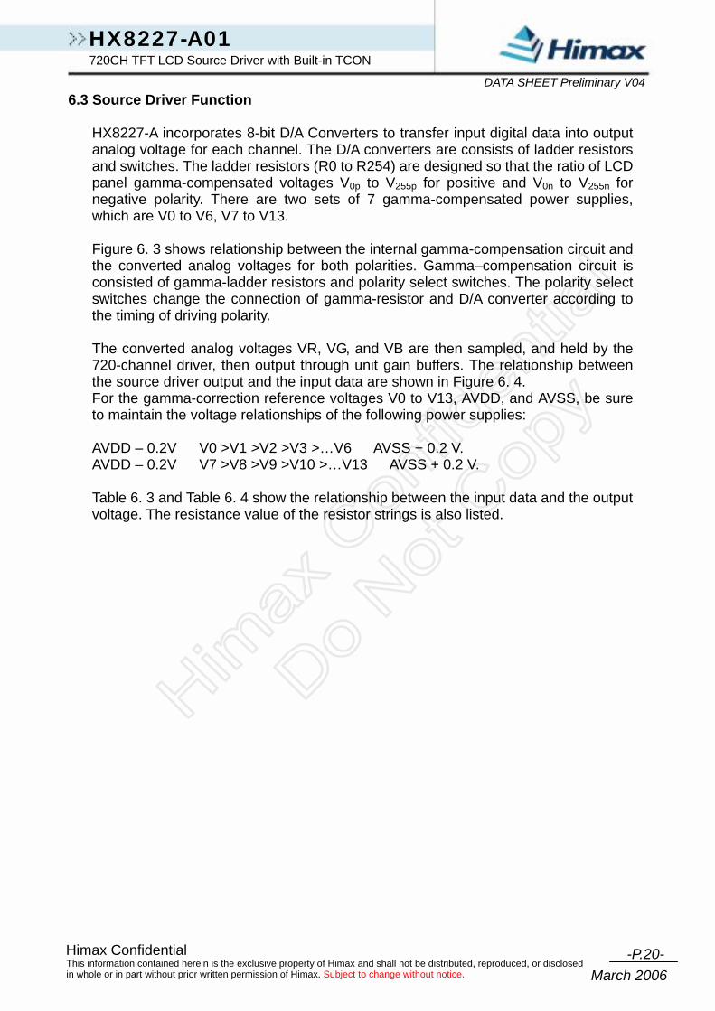
HX8227-A incorporates 8-bit D/A Converters to transfer input digital data into output analog voltage for each channel. The D/A converters are consists of ladder resistors and switches. The ladder resistors (R0 to R254) are designed so that the ratio of LCD panel gamma-compensated voltages V0p to V255p for positive and V0n to V255n for negative polarity. There are two sets of 7 gamma-compensated power supplies, which are V0 to V6, V7 to V13. Figure 6. 3 shows relationship between the internal gamma-compensation circuit and the converted analog voltages for both polarities. Gamma–compensation circuit is consisted of gamma-ladder resistors and polarity select switches. The polarity select switches change the connection of gamma-resistor and D/A converter according to the timing of driving polarity. The converted analog voltages VR, VG, and VB are then sampled, and held by the 720-channel driver, then output through unit gain buffers. The relationship between the source driver output and the input data are shown in Figure 6. 4. For the gamma-correction reference voltages V0 to V13, AVDD, and AVSS, be sure to maintain the voltage relationships of the following power supplies: AVDD – 0.2V V0 >V1 >V2 >V3 >…V6 AVSS + 0.2 V.≧ ≧ AVDD – 0.2V V7 >V8 >V9 >V10 >…V13 AVSS + ≧ ≧ 0.2 V. Table 6. 3 and Table 6. 4 show the relationship between the input data and the output voltage. The resistance value of the resistor strings is also listed.

-P.21- Himax Confidential
March 2006 This information contained herein is the exclusive property of Himax and shall not be distributed, reproduced, or disclosed in whole or in part without prior written permission of Himax. Subject to change without notice.
HX8227-A01 720CH TFT LCD Source Driver with Built-in TCON
DATA SHEET Preliminary V04
V0
V1
V2
V3
V4
V5
V6
r0
r1
r29
r30
r31
r32
r61
r62
r63
r64
r125
r126
r127
r128
r189
r190
r191
r192
r221
r222
r223
r224
r253
r254V0p
V32p
V64p
V128p
V192p
V224p
V255pV7
V8
V9
V10
V11
V12
V13 r0
r1
r29
r30
r31
r32
r61
r62
r63
r64
r125
r126
r127
r128
r189
r190
r191
r192
r221
r222
r223
r224
r253
r254
V255n
V224n
V192n
V128n
V64n
V32n
V0n
VR
VG
VB
3 D/A ConvertersPolarity Select Switches
Positive
Negative
Gamma Resistor Strings
Positive Negative
Figure 6. 3 Relationship between the internal gamma-compensation circuits
Positive Polarity
Negative Polarity
0 255Gray Level
Out
put V
olta
ge
Source driverOutput Voltage
NB: PositiveNW: Negative
COMSIG
COMOUT(Gate Driver)
COMH
COML
DVDD
DVSS
NB: NegativeNW: Positive
Figure 6. 4 Relationship between NB and NW output polarity
-P.22- Himax Confidential
March 2006 This information contained herein is the exclusive property of Himax and shall not be distributed, reproduced, or disclosed in whole or in part without prior written permission of Himax. Subject to change without notice.
HX8227-A01 720CH TFT LCD Source Driver with Built-in TCON
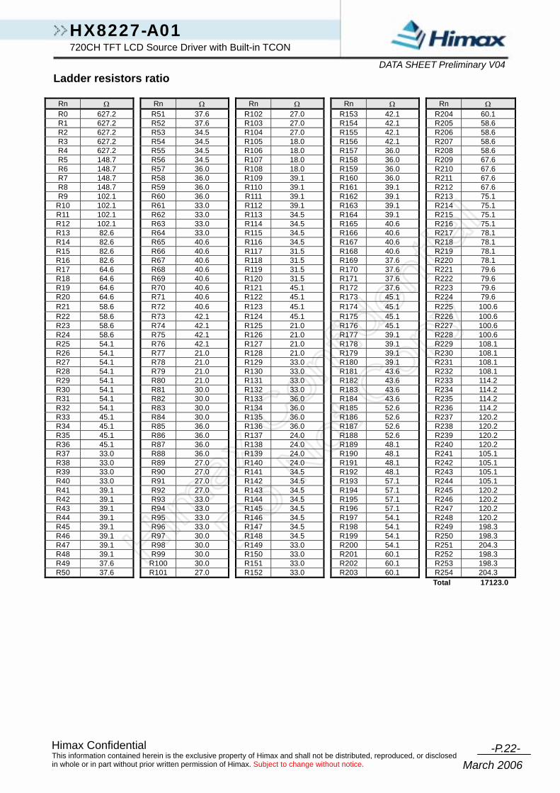
DATA SHEET Preliminary V04Ladder resistors ratio
Rn Ω Rn Ω Rn Ω Rn Ω Rn Ω R0 627.2 R51 37.6 R102 27.0 R153 42.1 R204 60.1 R1 627.2 R52 37.6 R103 27.0 R154 42.1 R205 58.6 R2 627.2 R53 34.5 R104 27.0 R155 42.1 R206 58.6 R3 627.2 R54 34.5 R105 18.0 R156 42.1 R207 58.6 R4 627.2 R55 34.5 R106 18.0 R157 36.0 R208 58.6 R5 148.7 R56 34.5 R107 18.0 R158 36.0 R209 67.6 R6 148.7 R57 36.0 R108 18.0 R159 36.0 R210 67.6 R7 148.7 R58 36.0 R109 39.1 R160 36.0 R211 67.6 R8 148.7 R59 36.0 R110 39.1 R161 39.1 R212 67.6 R9 102.1 R60 36.0 R111 39.1 R162 39.1 R213 75.1
R10 102.1 R61 33.0 R112 39.1 R163 39.1 R214 75.1 R11 102.1 R62 33.0 R113 34.5 R164 39.1 R215 75.1 R12 102.1 R63 33.0 R114 34.5 R165 40.6 R216 75.1 R13 82.6 R64 33.0 R115 34.5 R166 40.6 R217 78.1 R14 82.6 R65 40.6 R116 34.5 R167 40.6 R218 78.1 R15 82.6 R66 40.6 R117 31.5 R168 40.6 R219 78.1 R16 82.6 R67 40.6 R118 31.5 R169 37.6 R220 78.1 R17 64.6 R68 40.6 R119 31.5 R170 37.6 R221 79.6 R18 64.6 R69 40.6 R120 31.5 R171 37.6 R222 79.6 R19 64.6 R70 40.6 R121 45.1 R172 37.6 R223 79.6 R20 64.6 R71 40.6 R122 45.1 R173 45.1 R224 79.6 R21 58.6 R72 40.6 R123 45.1 R174 45.1 R225 100.6 R22 58.6 R73 42.1 R124 45.1 R175 45.1 R226 100.6 R23 58.6 R74 42.1 R125 21.0 R176 45.1 R227 100.6 R24 58.6 R75 42.1 R126 21.0 R177 39.1 R228 100.6 R25 54.1 R76 42.1 R127 21.0 R178 39.1 R229 108.1 R26 54.1 R77 21.0 R128 21.0 R179 39.1 R230 108.1 R27 54.1 R78 21.0 R129 33.0 R180 39.1 R231 108.1 R28 54.1 R79 21.0 R130 33.0 R181 43.6 R232 108.1 R29 54.1 R80 21.0 R131 33.0 R182 43.6 R233 114.2 R30 54.1 R81 30.0 R132 33.0 R183 43.6 R234 114.2 R31 54.1 R82 30.0 R133 36.0 R184 43.6 R235 114.2 R32 54.1 R83 30.0 R134 36.0 R185 52.6 R236 114.2 R33 45.1 R84 30.0 R135 36.0 R186 52.6 R237 120.2 R34 45.1 R85 36.0 R136 36.0 R187 52.6 R238 120.2 R35 45.1 R86 36.0 R137 24.0 R188 52.6 R239 120.2 R36 45.1 R87 36.0 R138 24.0 R189 48.1 R240 120.2 R37 33.0 R88 36.0 R139 24.0 R190 48.1 R241 105.1 R38 33.0 R89 27.0 R140 24.0 R191 48.1 R242 105.1 R39 33.0 R90 27.0 R141 34.5 R192 48.1 R243 105.1 R40 33.0 R91 27.0 R142 34.5 R193 57.1 R244 105.1 R41 39.1 R92 27.0 R143 34.5 R194 57.1 R245 120.2 R42 39.1 R93 33.0 R144 34.5 R195 57.1 R246 120.2 R43 39.1 R94 33.0 R145 34.5 R196 57.1 R247 120.2 R44 39.1 R95 33.0 R146 34.5 R197 54.1 R248 120.2 R45 39.1 R96 33.0 R147 34.5 R198 54.1 R249 198.3 R46 39.1 R97 30.0 R148 34.5 R199 54.1 R250 198.3 R47 39.1 R98 30.0 R149 33.0 R200 54.1 R251 204.3 R48 39.1 R99 30.0 R150 33.0 R201 60.1 R252 198.3 R49 37.6 R100 30.0 R151 33.0 R202 60.1 R253 198.3 R50 37.6 R101 27.0 R152 33.0 R203 60.1 R254 204.3
Total 17123.0

-P.23- Himax Confidential
March 2006 This information contained herein is the exclusive property of Himax and shall not be distributed, reproduced, or disclosed in whole or in part without prior written permission of Himax. Subject to change without notice.
HX8227-A01 720CH TFT LCD Source Driver with Built-in TCON
DATA SHEET Preliminary V04Input data and output voltage
INPUT DATA OUTPUT VOLTAGE Hex Dx7 Dx6 Dx5 Dx4 Dx3 Dx2 Dx1 Dx0 Positive Negative
0 0 0 0 0 0 0 0 0 V6 V7 1 0 0 0 0 0 0 0 1 V6+(V5-V6)*(204.3 /4034.4 ) V8+(V7-V8)*(3830.1/4034.4 ) 2 0 0 0 0 0 0 1 0 V6+(V5-V6)*(402.5/4034.4 ) V8+(V7-V8)*(3631.9/4034.4 ) 3 0 0 0 0 0 0 1 1 V6+(V5-V6)*(600.8.0/4034.4 ) V8+(V7-V8)*(3433.6/4034.4 ) 4 0 0 0 0 0 1 0 0 V6+(V5-V6)*(805.1/4034.4 ) V8+(V7-V8)*(3229.3/4034.4 ) 5 0 0 0 0 0 1 0 1 V6+(V5-V6)*(1003.3/4034.4 ) V8+(V7-V8)*(3031.1/4034.4 ) 6 0 0 0 0 0 1 1 0 V6+(V5-V6)*(1201.6/4034.4 ) V8+(V7-V8)*(2832.8/4034.4 ) 7 0 0 0 0 0 1 1 1 V6+(V5-V6)*(1321.8/4034.4 ) V8+(V7-V8)*(2712.6/4034.4 ) 8 0 0 0 0 1 0 0 0 V6+(V5-V6)*(1441.9 /4034.4 ) V8+(V7-V8)*(2592.5/4034.4 ) 9 0 0 0 0 1 0 0 1 V6+(V5-V6)*(1562.1/4034.4 ) V8+(V7-V8)*(2472.3/4034.4 )
0A 0 0 0 0 1 0 1 0 V6+(V5-V6)*(1682.3/4034.4 ) V8+(V7-V8)*(2352.3/4034.4 ) 0B 0 0 0 0 1 0 1 1 V6+(V5-V6)*(1787.4/4034.4 ) V8+(V7-V8)*(2247.0/4034.4 ) 0C 0 0 0 0 1 1 0 0 V6+(V5-V6)*(1892.5/4034.4 ) V8+(V7-V8)*(2141.9/4034.4 ) 0D 0 0 0 0 1 1 0 1 V6+(V5-V6)*(1997.7/4034.4 ) V8+(V7-V8)*(2036.7/4034.4 ) 0E 0 0 0 0 1 1 1 0 V6+(V5-V6)*(2102.8/4034.4 ) V8+(V7-V8)*(1931.6/4034.4 ) 0F 0 0 0 0 1 1 1 1 V6+(V5-V6)*(2223.0 /4034.4 ) V8+(V7-V8)*(1811.4/4034.4 ) 10 0 0 0 1 0 0 0 0 V6+(V5-V6)*(2343.1/4034.4 ) V8+(V7-V8)*(1691.3/4034.4 ) 11 0 0 0 1 0 0 0 1 V6+(V5-V6)*(2463.3/4034.4 ) V8+(V7-V8)*(1571.1/4034.4 ) 12 0 0 0 1 0 0 1 0 V6+(V5-V6)*(2583.5/4034.4 ) V8+(V7-V8)*(1450.9/4034.4 ) 13 0 0 0 1 0 0 1 1 V6+(V5-V6)*(2697.6/4034.4 ) V8+(V7-V8)*(1336.8/4034.4 ) 14 0 0 0 1 0 1 0 0 V6+(V5-V6)*(2811.8/4034.4 ) V8+(V7-V8)*(1222.6/4034.4 ) 15 0 0 0 1 0 1 0 1 V6+(V5-V6)*(2925.9/4034.4 ) V8+(V7-V8)*(1108.5/4034.4 ) 16 0 0 0 1 0 1 1 0 V6+(V5-V6)*(3040.1/4034.4 ) V8+(V7-V8)*(994.3/4034.4 ) 17 0 0 0 1 0 1 1 1 V6+(V5-V6)*(3148.2 /4034.4 ) V8+(V7-V8)*(886.2/4034.4 ) 18 0 0 0 1 1 0 0 0 V6+(V5-V6)*(3256.4/4034.4 ) V8+(V7-V8)*(778.0/4034.4 ) 19 0 0 0 1 1 0 0 1 V6+(V5-V6)*(3364.5/4034.4 ) V8+(V7-V8)*(669.6/4034.4 ) 1A 0 0 0 1 1 0 1 0 V6+(V5-V6)*(3472.7/4034.4 ) V8+(V7-V8)*(561.8/4034.4 ) 1 B 0 0 0 1 1 0 1 1 V6+(V5-V6)*(3573.3/4034.4 ) V8+(V7-V8)*(461.1/4034.4 ) 1C 0 0 0 1 1 1 0 0 V6+(V5-V6)*(3673.9 1/4034.4 ) V8+(V7-V8)*(360.5/4034.4 ) 1 D 0 0 0 1 1 1 0 1 V6+(V5-V6)*(3774.6/4034.4 ) V8+(V7-V8)*(259.8/4034.4 ) 1 E 0 0 0 1 1 1 1 0 V6+(V5-V6)*(3875.2/4034.4 ) V8+(V7-V8)*(159.2/4034.4 ) 1 F 0 0 0 1 1 1 1 1 V6+(V5-V6)*(3954.8/4034.4 ) V8+(V7-V8)*(79.6/4034.4 ) 20 0 0 1 0 0 0 0 0 V5 V8 21 0 0 1 0 0 0 0 1 V5+(V4-V5)*(79.6/2057.8 ) V9+(V8-V9)*(1978.2/2057.8 ) 22 0 0 1 0 0 0 1 0 V5+(V4-V5)*(159.2/2057.8 ) V9+(V8-V9)*(1898.6/2057.8 ) 23 0 0 1 0 0 0 1 1 V5+(V4-V5)*(237.3/2057.8 ) V9+(V8-V9)*(1820.4/2057.8 ) 24 0 0 1 0 0 1 0 0 V5+(V4-V5)*(315.41/2057.8 ) V9+(V8-V9)*(1742.3/2057.8 ) 25 0 0 1 0 0 1 0 1 V5+(V4-V5)*(393.5/2057.8 ) V9+(V8-V9)*(1664.2/2057.8 ) 26 0 0 1 0 0 1 1 0 V5+(V4-V5)*(471.6/2057.8 ) V9+(V8-V9)*(1586.1/2057.8 ) 27 0 0 1 0 0 1 1 1 V5+(V4-V5)*(546.7/2057.8 ) V9+(V8-V9)*(1511.0/2057.8 ) 28 0 0 1 0 1 0 0 0 V5+(V4-V5)*(621.8/2057.8 ) V9+(V8-V9)*(1435.9/2057.8 ) 29 0 0 1 0 1 0 0 1 V5+(V4-V5)*(696.9/2057.8 ) V9+(V8-V9)*(1360.8/2057.8 ) 2A 0 0 1 0 1 0 1 0 V5+(V4-V5)*(772.0/2057.8 ) V9+(V8-V9)*(1285.7/2057.8 ) 2B 0 0 1 0 1 0 1 1 V5+(V4-V5)*(839.6/2057.8 ) V9+(V8-V9)*(1218.1/2057.8 ) 2C 0 0 1 0 1 1 0 0 V5+(V4-V5)*(907.2/2057.8 ) V9+(V8-V9)*(1150.5/2057.8 ) 2D 0 0 1 0 1 1 0 1 V5+(V4-V5)*(974.8/2057.8 ) V9+(V8-V9)*(1083.0/2057.8 ) 2E 0 0 1 0 1 1 1 0 V5+(V4-V5)*(1042.4/2057.8 ) V9+(V8-V9)*(1015.4/2057.8 ) 2F 0 0 1 0 1 1 1 1 V5+(V4-V5)*(1101.0 /2057.8 ) V9+(V8-V9)*(956.8/2057.8 ) 30 0 0 1 1 0 0 0 0 V5+(V4-V5)*(1159.6 /2057.8 ) V9+(V8-V9)*(898.2/2057.8 ) 31 0 0 1 1 0 0 0 1 V5+(V4-V5)*(1218.1/2057.8 ) V9+(V8-V9)*(839.6/2057.8 ) 32 0 0 1 1 0 0 1 0 V5+(V4-V5)*(1276.7/2057.8 ) V9+(V8-V9)*(781.0/2057.8 ) 33 0 0 1 1 0 0 1 1 V5+(V4-V5)*(1336.8/2057.8 ) V9+(V8-V9)*(721.0/2057.8 ) 34 0 0 1 1 0 1 0 0 V5+(V4-V5)*(1396.9/2057.8 ) V9+(V8-V9)*(660.9/2057.8 ) 35 0 0 1 1 0 1 0 1 V5+(V4-V5)*(1457.0/2057.8 ) V9+(V8-V9)*(600.8/2057.8 ) 36 0 0 1 1 0 1 1 0 V5+(V4-V5)*(1517.0 /2057.8 ) V9+(V8-V9)*(540.7/2057.8 ) 37 0 0 1 1 0 1 1 1 V5+(V4-V5)*(1571.1/2057.8 ) V9+(V8-V9)*(486.7/2057.8 ) 38 0 0 1 1 1 0 0 0 V5+(V4-V5)*(1625.2/2057.8 ) V9+(V8-V9)*(432.6/2057.8 ) 39 0 0 1 1 1 0 0 1 V5+(V4-V5)*(1679.3/2057.8 ) V9+(V8-V9)*(378.5/2057.8 ) 3A 0 0 1 1 1 0 1 0 V5+(V4-V5)*(1733.3/2057.8 ) V9+(V8-V9)*(324.4/2057.8 ) 3B 0 0 1 1 1 0 1 1 V5+(V4-V5)*(1790.4 /2057.8 ) V9+(V8-V9)*(267.4/2057.8 ) 3C 0 0 1 1 1 1 0 0 V5+(V4-V5)*(1847.5/2057.8 ) V9+(V8-V9)*(210.3/2057.8 ) 3D 0 0 1 1 1 1 0 1 V5+(V4-V5)*(1904.6/2057.8 ) V9+(V8-V9)*(153.2/2057.8 ) 3E 0 0 1 1 1 1 1 0 V5+(V4-V5)*(1961.6/2057.8 ) V9+(V8-V9)*(96.1/2057.8 ) 3F 0 0 1 1 1 1 1 1 V5+(V4-V5)*(2009.7/2057.8 ) V9+(V8-V9)*(48.1/2057.8 )

-P.24- Himax Confidential
March 2006 This information contained herein is the exclusive property of Himax and shall not be distributed, reproduced, or disclosed in whole or in part without prior written permission of Himax. Subject to change without notice.
HX8227-A01 720CH TFT LCD Source Driver with Built-in TCON
DATA SHEET Preliminary V04
INPUT DATA OUTPUT VOLTAGE Hex Dx7 Dx6 Dx5 Dx4 Dx3 Dx2 Dx1 Dx0 Positive Negative 40 0 1 0 0 0 0 0 0 V4 V9 41 0 1 0 0 0 0 0 1 V4+(V3-V4)*(48.1/2421.3 ) V10+(V9-V10)*(2373.2/2421.3 )42 0 1 0 0 0 0 1 0 V4+(V3-V4)*(96.1/2421.3 ) V10+(V9-V10)*(2352.1/2421.3 )43 0 1 0 0 0 0 1 1 V4+(V3-V4)*(148.7/2421.3 ) V10+(V9-V10)*(2272.6/2421.3 )44 0 1 0 0 0 1 0 0 V4+(V3-V4)*(201.3/2421.3 ) V10+(V9-V10)*(2220.0/2421.3 )45 0 1 0 0 0 1 0 1 V4+(V3-V4)*(253.8/2421.3 ) V10+(V9-V10)*(2167.4/2421.3 )46 0 1 0 0 0 1 1 0 V4+(V3-V4)*(306.4/2421.3 ) V10+(V9-V10)*(2114.8/2421.3 )47 0 1 0 0 0 1 1 1 V4+(V3-V4)*(350.0/2421.3 ) V10+(V9-V10)*(2071.3/2421.3 )48 0 1 0 0 1 0 0 0 V4+(V3-V4)*(393.5/2421.3 ) V10+(V9-V10)*(2027.7/2421.3 )49 0 1 0 0 1 0 0 1 V4+(V3-V4)*(437.1/2421.3 ) V10+(V9-V10)*(1984.2/2421.3 )4A 0 1 0 0 1 0 1 0 V4+(V3-V4)*(480.6/2421.3 ) V10+(V9-V10)*(1940.6/2421.3 )4B 0 1 0 0 1 0 1 1 V4+(V3-V4)*(519.7/2421.3 ) V10+(V9-V10)*(1901.6/2421.3 )4C 0 1 0 0 1 1 0 0 V4+(V3-V4)*(558.8/2421.3 ) V10+(V9-V10)*(1862.5/2421.3 )4D 0 1 0 0 1 1 0 1 V4+(V3-V4)*(597.8/2421.3 ) V10+(V9-V10)*(1823.4/2421.3 )4E 0 1 0 0 1 1 1 0 V4+(V3-V4)*(636.9/2421.3 ) V10+(V9-V10)*(1784.4/2421.3 )4F 0 1 0 0 1 1 1 1 V4+(V3-V4)*(681.9/2421.3 ) V10+(V9-V10)*(1739.3/2421.3 )50 0 1 0 1 0 0 0 0 V4+(V3-V4)*(727.0/2421.3 ) V10+(V9-V10)*(1694.3/2421.3 )51 0 1 0 1 0 0 0 1 V4+(V3-V4)*(772.0/2421.3 ) V10+(V9-V10)*(1649.2/2421.3 )52 0 1 0 1 0 0 1 0 V4+(V3-V4)*(817.1/2421.3 ) V10+(V9-V10)*(1604.2/2421.3 )53 0 1 0 1 0 0 1 1 V4+(V3-V4)*(854.6/2421.3 ) V10+(V9-V10)*(1566.6/2421.3 )54 0 1 0 1 0 1 0 0 V4+(V3-V4)*(892.2/2421.3 ) V10+(V9-V10)*(1529.1/2421.3 )55 0 1 0 1 0 1 0 1 V4+(V3-V4)*(929.7/2421.3 ) V10+(V9-V10)*(1491.5/2421.3 )56 0 1 0 1 0 1 1 0 V4+(V3-V4)*(967.3/2421.3 ) V10+(V9-V10)*(1454.0/2421.3 )57 0 1 0 1 0 1 1 1 V4+(V3-V4)*(1007.9/2421.3 ) V10+(V9-V10)*(1413.4/2421.3 )58 0 1 0 1 1 0 0 0 V4+(V3-V4)*(1048.4/2421.3 ) V10+(V9-V10)*(1372.8/2421.3 )59 0 1 0 1 1 0 0 1 V4+(V3-V4)*(1089.0/2421.3 ) V10+(V9-V10)*(1332.3/2421.3 )5A 0 1 0 1 1 0 1 0 V4+(V3-V4)*(1129.5/2421.3 ) V10+(V9-V10)*(1291.7/2421.3 )5B 0 1 0 1 1 0 1 1 V4+(V3-V4)*(1168.6/2421.3 ) V10+(V9-V10)*(1252.7/2421.3 )5C 0 1 0 1 1 1 0 0 V4+(V3-V4)*(1207.6/2421.3 ) V10+(V9-V10)*(1213.6/2421.3 )5D 0 1 0 1 1 1 0 1 V4+(V3-V4)*(1246.7/2421.3 ) V10+(V9-V10)*(1174.6/2421.3 )5E 0 1 0 1 1 1 1 0 V4+(V3-V4)*(1285.7/2421.3 ) V10+(V9-V10)*(1135.5/2421.3 )5F 0 1 0 1 1 1 1 1 V4+(V3-V4)*(1321.8/2421.3 ) V10+(V9-V10)*(1099.5/2421.3 )60 0 1 1 0 0 0 0 0 V4+(V3-V4)*(1357.8/2421.3 ) V10+(V9-V10)*(1063.4/2421.3 )61 0 1 1 0 0 0 0 1 V4+(V3-V4)*(1393.9/2421.3 ) V10+(V9-V10)*(1027.4/2421.3 )62 0 1 1 0 0 0 1 0 V4+(V3-V4)*(1429.9/2421.3 ) V10+(V9-V10)*(991.3/2421.3 )63 0 1 1 0 0 0 1 1 V4+(V3-V4)*(1472.0/2421.3 ) V10+(V9-V10)*(949.3/2421.3 )64 0 1 1 0 0 1 0 0 V4+(V3-V4)*(1514.0/2421.3 ) V10+(V9-V10)*(907.2/2421.3 )65 0 1 1 0 0 1 0 1 V4+(V3-V4)*(1556.1/2421.3 ) V10+(V9-V10)*(865.2/2421.3 )66 0 1 1 0 0 1 1 0 V4+(V3-V4)*(1598.1/2421.3 ) V10+(V9-V10)*(823.1/2421.3 )67 0 1 1 0 0 1 1 1 V4+(V3-V4)*(1631.2/2421.3 ) V10+(V9-V10)*(790.1/2421.3 )68 0 1 1 0 1 0 0 0 V4+(V3-V4)*(1664.2/2421.3 ) V10+(V9-V10)*(757.0/2421.3 )69 0 1 1 0 1 0 0 1 V4+(V3-V4)*(1697.3/2421.3 ) V10+(V9-V10)*(724.0/2421.3 )6A 0 1 1 0 1 0 1 0 V4+(V3-V4)*(1730.3/2421.3 ) V10+(V9-V10)*(690.9/2421.3 )6B 0 1 1 0 1 0 1 1 V4+(V3-V4)*(1764.9/2421.3 ) V10+(V9-V10)*(656.4/2421.3 )6C 0 1 1 0 1 1 0 0 V4+(V3-V4)*(1799.4/2421.3 ) V10+(V9-V10)*(621.8/2421.3 )6D 0 1 1 0 1 1 0 1 V4+(V3-V4)*(1834.0/2421.3 ) V10+(V9-V10)*(587.3/2421.3 )6E 0 1 1 0 1 1 1 0 V4+(V3-V4)*(1868.5/2421.3 ) V10+(V9-V10)*(552.7/2421.3 )6F 0 1 1 0 1 1 1 1 V4+(V3-V4)*(1903.1/2421.3 ) V10+(V9-V10)*(518.2/2421.3 )70 0 1 1 1 0 0 0 0 V4+(V3-V4)*(1937.6/2421.3 ) V10+(V9-V10)*(483.6/2421.3 )71 0 1 1 1 0 0 0 1 V4+(V3-V4)*(1972.1/2421.3 ) V10+(V9-V10)*(449.1/2421.3 )72 0 1 1 1 0 0 1 0 V4+(V3-V4)*(2006.7/2421.3 ) V10+(V9-V10)*(414.6/2421.3 )73 0 1 1 1 0 0 1 1 V4+(V3-V4)*(2030.7/2421.3 ) V10+(V9-V10)*(390.5/2421.3 )74 0 1 1 1 0 1 0 0 V4+(V3-V4)*(2054.8/2421.3 ) V10+(V9-V10)*(366.5/2421.3 )75 0 1 1 1 0 1 0 1 V4+(V3-V4)*(2078.8/2421.3 ) V10+(V9-V10)*(342.5/2421.3 )76 0 1 1 1 0 1 1 0 V4+(V3-V4)*(2102.8/2421.3 ) V10+(V9-V10)*(318.4/2421.3 )77 0 1 1 1 0 1 1 1 V4+(V3-V4)*(2138.9/2421.3 ) V10+(V9-V10)*(282.4/2421.3 )78 0 1 1 1 1 0 0 0 V4+(V3-V4)*(2174.9/2421.3 ) V10+(V9-V10)*(246.3/2421.3 )79 0 1 1 1 1 0 0 1 V4+(V3-V4)*(2211.0/2421.3 ) V10+(V9-V10)*(210.3/2421.3 )7A 0 1 1 1 1 0 1 0 V4+(V3-V4)*(2247.0/2421.3 ) V10+(V9-V10)*(174.2/2421.3 )7B 0 1 1 1 1 0 1 1 V4+(V3-V4)*(2280.1/2421.3 ) V10+(V9-V10)*(141.2/2421.3 )7C 0 1 1 1 1 1 0 0 V4+(V3-V4)*(2313.1/2421.3 ) V10+(V9-V10)*(108.1/2421.3 )7D 0 1 1 1 1 1 0 1 V4+(V3-V4)*(2346.2/2421.3 ) V10+(V9-V10)*(75.1/2421.3 ) 7E 0 1 1 1 1 1 1 0 V4+(V3-V4)*(2379.2/2421.3 ) V10+(V9-V10)*(42.1/2421.3 ) 7F 0 1 1 1 1 1 1 1 V4+(V3-V4)*(2400.2/2421.3 ) V10+(V9-V10)*(21.0/2421.3 )

-P.25- Himax Confidential
March 2006 This information contained herein is the exclusive property of Himax and shall not be distributed, reproduced, or disclosed in whole or in part without prior written permission of Himax. Subject to change without notice.
HX8227-A01 720CH TFT LCD Source Driver with Built-in TCON
DATA SHEET Preliminary V04
INPUT DATA OUTPUT VOLTAGE
Hex Dx7 Dx6 Dx5 Dx4 Dx3 Dx2 Dx1 Dx0 Positive Negative 80 1 0 0 0 0 0 0 0 V3 V10 81 1 0 0 0 0 0 0 1 V3+(V2-V3)*(21.0/2090.8 ) V11+(V10-V11)*(2069.8/2090.8 )82 1 0 0 0 0 0 1 0 V3+(V2-V3)*(42.1/2090.8 ) V11+(V10-V11)*(2048.8/2090.8 ) 83 1 0 0 0 0 0 1 1 V3+(V2-V3)*(87.1/2090.8 ) V11+(V10-V11)*(2003.7/2090.8 )84 1 0 0 0 0 1 0 0 V3+(V2-V3)*(132.2/2090.8 ) V11+(V10-V11)*(1958.6/2090.8 ) 85 1 0 0 0 0 1 0 1 V3+(V2-V3)*(177.2/2090.8 ) V11+(V10-V11)*(1913.6/2090.8 )86 1 0 0 0 0 1 1 0 V3+(V2-V3)*(222.3/2090.8 ) V11+(V10-V11)*(1868.5/2090.8 ) 87 1 0 0 0 0 1 1 1 V3+(V2-V3)*(253.8/2090.8 ) V11+(V10-V11)*(1837.0/2090.8 )88 1 0 0 0 1 0 0 0 V3+(V2-V3)*(285.4/2090.8 ) V11+(V10-V11)*(1805.4/2090.8 ) 89 1 0 0 0 1 0 0 1 V3+(V2-V3)*(316.9/2090.8 ) V11+(V10-V11)*(1773.9/2090.8 )8A 1 0 0 0 1 0 1 0 V3+(V2-V3)*(348.5/2090.8 ) V11+(V10-V11)*(1742.3/2090.8 ) 8B 1 0 0 0 1 0 1 1 V3+(V2-V3)*(383.0/2090.8 ) V11+(V10-V11)*(1707.8/2090.8 )8C 1 0 0 0 1 1 0 0 V3+(V2-V3)*(417.6/2090.8 ) V11+(V10-V11)*(1673.2/2090.8 ) 8D 1 0 0 0 1 1 0 1 V3+(V2-V3)*(452.1/2090.8 ) V11+(V10-V11)*(1638.7/2090.8 )8E 1 0 0 0 1 1 1 0 V3+(V2-V3)*(486.7/2090.8 ) V11+(V10-V11)*(1604.2/2090.8 ) 8F 1 0 0 0 1 1 1 1 V3+(V2-V3)*(525.7/2090.8 ) V11+(V10-V11)*(1565.1/2090.8 )90 1 0 0 1 0 0 0 0 V3+(V2-V3)*(564.8/2090.8 ) V11+(V10-V11)*(1526.0/2090.8 )91 1 0 0 1 0 0 0 1 V3+(V2-V3)*(603.8/2090.8 ) V11+(V10-V11)*(1487.0/2090.8 ) 92 1 0 0 1 0 0 1 0 V3+(V2-V3)*(642.9/2090.8 ) V11+(V10-V11)*(1447.9/2090.8 )93 1 0 0 1 0 0 1 1 V3+(V2-V3)*(660.9/2090.8 ) V11+(V10-V11)*(1429.9/2090.8 ) 94 1 0 0 1 0 1 0 0 V3+(V2-V3)*(678.9/2090.8 ) V11+(V10-V11)*(1411.9/2090.8 )95 1 0 0 1 0 1 0 1 V3+(V2-V3)*(696.9/2090.8 ) V11+(V10-V11)*(1393.9/2090.8 ) 96 1 0 0 1 0 1 1 0 V3+(V2-V3)*(715.0/2090.8 ) V11+(V10-V11)*(1375.8/2090.8 )97 1 0 0 1 0 1 1 1 V3+(V2-V3)*(742.0/2090.8 ) V11+(V10-V11)*(1348.8/2090.8 ) 98 1 0 0 1 1 0 0 0 V3+(V2-V3)*(769.0/2090.8 ) V11+(V10-V11)*(1321.8/2090.8 )99 1 0 0 1 1 0 0 1 V3+(V2-V3)*(796.1/2090.8 ) V11+(V10-V11)*(1294.7/2090.8 ) 9A 1 0 0 1 1 0 1 0 V3+(V2-V3)*(823.1/2090.8 ) V11+(V10-V11)*(1267.7/2090.8 )9B 1 0 0 1 1 0 1 1 V3+(V2-V3)*(853.1/2090.8 ) V11+(V10-V11)*(1237.7/2090.8 ) 9C 1 0 0 1 1 1 0 0 V3+(V2-V3)*(883.2/2090.8 ) V11+(V10-V11)*(1207.6/2090.8 )9D 1 0 0 1 1 1 0 1 V3+(V2-V3)*(913.2/2090.8 ) V11+(V10-V11)*(1177.6/2090.8 ) 9E 1 0 0 1 1 1 1 0 V3+(V2-V3)*(943.3/2090.8 ) V11+(V10-V11)*(1147.5/2090.8 )9F 1 0 0 1 1 1 1 1 V3+(V2-V3)*(976.3/2090.8 ) V11+(V10-V11)*(1114.5/2090.8 ) A0 1 0 1 0 0 0 0 0 V3+(V2-V3)*(1009.4/2090.8 ) V11+(V10-V11)*(1081.5/2090.8 )A1 1 0 1 0 0 0 0 1 V3+(V2-V3)*(1042.4/2090.8 ) V11+(V10-V11)*(1048.4/2090.8 ) A2 1 0 1 0 0 0 1 0 V3+(V2-V3)*(1075.4/2090.8 ) V11+(V10-V11)*(1015.4/2090.8 )A3 1 0 1 0 0 0 1 1 V3+(V2-V3)*(1102.5/2090.8 ) V11+(V10-V11)*(988.3/2090.8 ) A4 1 0 1 0 0 1 0 0 V3+(V2-V3)*(1129.5/2090.8 ) V11+(V10-V11)*(961.3/2090.8 )A5 1 0 1 0 0 1 0 1 V3+(V2-V3)*(1156.6/2090.8 ) V11+(V10-V11)*(934.3/2090.8 ) A6 1 0 1 0 0 1 1 0 V3+(V2-V3)*(1183.6/2090.8 ) V11+(V10-V11)*(907.2/2090.8 )A7 1 0 1 0 0 1 1 1 V3+(V2-V3)*(1219.6/2090.8 ) V11+(V10-V11)*(871.2/2090.8 ) A8 1 0 1 0 1 0 0 0 V3+(V2-V3)*(1255.7/2090.8 ) V11+(V10-V11)*(835.1/2090.8 )A9 1 0 1 0 1 0 0 1 V3+(V2-V3)*(1291.7/2090.8 ) V11+(V10-V11)*(799.1/2090.8 )AA 1 0 1 0 1 0 1 0 V3+(V2-V3)*(1327.8/2090.8 ) V11+(V10-V11)*(763.0/2090.8 ) AB 1 0 1 0 1 0 1 1 V3+(V2-V3)*(1357.8/2090.8 ) V11+(V10-V11)*(733.0/2090.8 )AC 1 0 1 0 1 1 0 0 V3+(V2-V3)*(1387.9/2090.8 ) V11+(V10-V11)*(702.9/2090.8 ) AD 1 0 1 0 1 1 0 1 V3+(V2-V3)*(1417.9/2090.8 ) V11+(V10-V11)*(672.9/2090.8 )AE 1 0 1 0 1 1 1 0 V3+(V2-V3)*(1447.9/2090.8 ) V11+(V10-V11)*(642.9/2090.8 ) AF 1 0 1 0 1 1 1 1 V3+(V2-V3)*(1469.0/2090.8 ) V11+(V10-V11)*(621.8/2090.8 )B0 1 0 1 1 0 0 0 0 V3+(V2-V3)*(1490.0/2090.8 ) V11+(V10-V11)*(600.8/2090.8 ) B1 1 0 1 1 0 0 0 1 V3+(V2-V3)*(1511.0/2090.8 ) V11+(V10-V11)*(579.8/2090.8 )B2 1 0 1 1 0 0 1 0 V3+(V2-V3)*(1532.1/2090.8 ) V11+(V10-V11)*(558.8/2090.8 ) B3 1 0 1 1 0 0 1 1 V3+(V2-V3)*(1574.1/2090.8 ) V11+(V10-V11)*(516.7/2090.8 )B4 1 0 1 1 0 1 0 0 V3+(V2-V3)*(1616.2/2090.8 ) V11+(V10-V11)*(474.6/2090.8 ) B5 1 0 1 1 0 1 0 1 V3+(V2-V3)*(1658.2/2090.8 ) V11+(V10-V11)*(432.6/2090.8 )B6 1 0 1 1 0 1 1 0 V3+(V2-V3)*(1700.3/2090.8 ) V11+(V10-V11)*(390.5/2090.8 ) B7 1 0 1 1 0 1 1 1 V3+(V2-V3)*(1740.8/2090.8 ) V11+(V10-V11)*(350.0/2090.8 )B8 1 0 1 1 1 0 0 0 V3+(V2-V3)*(1781.4/2090.8 ) V11+(V10-V11)*(309.4/2090.8 ) B9 1 0 1 1 1 0 0 1 V3+(V2-V3)*(1821.9/2090.8 ) V11+(V10-V11)*(268.9/2090.8 )BA 1 0 1 1 1 0 1 0 V3+(V2-V3)*(1862.5/2090.8 ) V11+(V10-V11)*(228.3/2090.8 ) BB 1 0 1 1 1 0 1 1 V3+(V2-V3)*(1903.1/2090.8 ) V11+(V10-V11)*(187.8/2090.8 )BC 1 0 1 1 1 1 0 0 V3+(V2-V3)*(1943.6/2090.8 ) V11+(V10-V11)*(147.2/2090.8 ) BD 1 0 1 1 1 1 0 1 V3+(V2-V3)*(1984.2/2090.8 ) V11+(V10-V11)*(106.6/2090.8 )BE 1 0 1 1 1 1 1 0 V3+(V2-V3)*(2024.7/2090.8 ) V11+(V10-V11)*(66.1/2090.8 ) BF 1 0 1 1 1 1 1 1 V3+(V2-V3)*(2057.8/2090.8 ) V11+(V10-V11)*(33.0/2090.8 )

-P.26- Himax Confidential
March 2006 This information contained herein is the exclusive property of Himax and shall not be distributed, reproduced, or disclosed in whole or in part without prior written permission of Himax. Subject to change without notice.
HX8227-A01 720CH TFT LCD Source Driver with Built-in TCON
DATA SHEET Preliminary V04
INPUT DATA OUTPUT DATA
Hex Dx7 Dx6 Dx5 Dx4 Dx3 Dx2 Dx1 Dx0 Positive Negative C0 1 1 0 0 0 0 0 0 V2 V11 C1 1 1 0 0 0 0 0 1 V2+(V1-V2)*(33.0/1231.7 ) V12+(V11-V12)*(1198.6/1231.7 )C2 1 1 0 0 0 0 1 0 V2+(V1-V2)*(66.1/1231.7 ) V12+(V11-V12)*(1165.6/1231.7 ) C3 1 1 0 0 0 0 1 1 V2+(V1-V2)*(102.1/1231.7 ) V12+(V11-V12)*(1129.5/1231.7 )C4 1 1 0 0 0 1 0 0 V2+(V1-V2)*(138.2/1231.7 ) V12+(V11-V12)*(1093.5/1231.7 ) C5 1 1 0 0 0 1 0 1 V2+(V1-V2)*(174.2/1231.7 ) V12+(V11-V12)*(1057.4/1231.7 )C6 1 1 0 0 0 1 1 0 V2+(V1-V2)*(210.3/1231.7 ) V12+(V11-V12)*(1021.4/1231.7 ) C7 1 1 0 0 0 1 1 1 V2+(V1-V2)*(244.8/1231.7 ) V12+(V11-V12)*(986.8/1231.7 )C8 1 1 0 0 1 0 0 0 V2+(V1-V2)*(279.4/1231.7 ) V12+(V11-V12)*(952.3/1231.7 ) C9 1 1 0 0 1 0 0 1 V2+(V1-V2)*(313.9/1231.7 ) V12+(V11-V12)*(917.7/1231.7 )CA 1 1 0 0 1 0 1 0 V2+(V1-V2)*(348.5/1231.7 ) V12+(V11-V12)*(883.2/1231.7 ) CB 1 1 0 0 1 0 1 1 V2+(V1-V2)*(386.0/1231.7 ) V12+(V11-V12)*(845.6/1231.7 )CC 1 1 0 0 1 1 0 0 V2+(V1-V2)*(423.6/1231.7 ) V12+(V11-V12)*(808.1/1231.7 ) CD 1 1 0 0 1 1 0 1 V2+(V1-V2)*(461.1/1231.7 ) V12+(V11-V12)*(770.5/1231.7 )CE 1 1 0 0 1 1 1 0 V2+(V1-V2)*(498.7/1231.7 ) V12+(V11-V12)*(733.0/1231.7 ) CF 1 1 0 0 1 1 1 1 V2+(V1-V2)*(537.7/1231.7 ) V12+(V11-V12)*(693.9/1231.7 )D0 1 1 0 1 0 0 0 0 V2+(V1-V2)*(576.8/1231.7 ) V12+(V11-V12)*(654.9/1231.7 )D1 1 1 0 1 0 0 0 1 V2+(V1-V2)*(615.8/1231.7 ) V12+(V11-V12)*(615.8/1231.7 ) D2 1 1 0 1 0 0 1 0 V2+(V1-V2)*(654.9/1231.7 ) V12+(V11-V12)*(576.8/1231.7 )D3 1 1 0 1 0 0 1 1 V2+(V1-V2)*(693.9/1231.7 ) V12+(V11-V12)*(537.7/1231.7 ) D4 1 1 0 1 0 1 0 0 V2+(V1-V2)*(733.0/1231.7 ) V12+(V11-V12)*(498.7/1231.7 )D5 1 1 0 1 0 1 0 1 V2+(V1-V2)*(772.0/1231.7 ) V12+(V11-V12)*(459.6/1231.7 ) D6 1 1 0 1 0 1 1 0 V2+(V1-V2)*(811.1/1231.7 ) V12+(V11-V12)*(420.6/1231.7 )D7 1 1 0 1 0 1 1 1 V2+(V1-V2)*(844.1/1231.7 ) V12+(V11-V12)*(387.5/1231.7 ) D8 1 1 0 1 1 0 0 0 V2+(V1-V2)*(877.2/1231.7 ) V12+(V11-V12)*(354.5/1231.7 )D9 1 1 0 1 1 0 0 1 V2+(V1-V2)*(910.2/1231.7 ) V12+(V11-V12)*(321.4/1231.7 ) DA 1 1 0 1 1 0 1 0 V2+(V1-V2)*(943.3/1231.7 ) V12+(V11-V12)*(288.4/1231.7 )DB 1 1 0 1 1 0 1 1 V2+(V1-V2)*(988.3/1231.7 ) V12+(V11-V12)*(243.3/1231.7 ) DC 1 1 0 1 1 1 0 0 V2+(V1-V2)*(1033.4/1231.7 ) V12+(V11-V12)*(198.3/1231.7 )DD 1 1 0 1 1 1 0 1 V2+(V1-V2)*(1078.4/1231.7 ) V12+(V11-V12)*(153.2/1231.7 ) DE 1 1 0 1 1 1 1 0 V2+(V1-V2)*(1123.5/1231.7 ) V12+(V11-V12)*(108.1/1231.7 )DF 1 1 0 1 1 1 1 1 V2+(V1-V2)*(1177.6/1231.7 ) V12+(V11-V12)*(54.1/1231.7 ) E0 1 1 1 0 0 0 0 0 V1 V12 E1 1 1 1 0 0 0 0 1 V1+(V0-V1)*(54.1/5287.1 ) 13+(V12-V13)*(5233.0/5287.1 ) E2 1 1 1 0 0 0 1 0 V1+(V0-V1)*(108.1/5287.1 ) 13+(V12-V13)*(5179.0/5287.1 )E3 1 1 1 0 0 0 1 1 V1+(V0-V1)*(162.2/5287.1 ) 13+(V12-V13)*(5124.9/5287.1 ) E4 1 1 1 0 0 1 0 0 V1+(V0-V1)*(216.3/5287.1 ) 13+(V12-V13)*(5070.8/5287.1 )E5 1 1 1 0 0 1 0 1 V1+(V0-V1)*(270.4/5287.1 ) 13+(V12-V13)*(5016.7/5287.1 ) E6 1 1 1 0 0 1 1 0 V1+(V0-V1)*(324.4/5287.1 ) 13+(V12-V13)*(4962.7/5287.1 )E7 1 1 1 0 0 1 1 1 V1+(V0-V1)*(383.0/5287.1 ) 13+(V12-V13)*(4904.1/5287.1 ) E8 1 1 1 0 1 0 0 0 V1+(V0-V1)*(441.6/5287.1 ) 13+(V12-V13)*(4845.5/5287.1 )E9 1 1 1 0 1 0 0 1 V1+(V0-V1)*(500.2/5287.1 ) 13+(V12-V13)*(4786.9/5287.1 )EA 1 1 1 0 1 0 1 0 V1+(V0-V1)*(558.8/5287.1 ) 13+(V12-V13)*(4728.4/5287.1 ) EB 1 1 1 0 1 0 1 1 V1+(V0-V1)*(623.3/5287.1 ) 13+(V12-V13)*(4663.8/5287.1 )EC 1 1 1 0 1 1 0 0 V1+(V0-V1)*(687.9/5287.1 ) 13+(V12-V13)*(4599.2/5287.1 ) ED 1 1 1 0 1 1 0 1 V1+(V0-V1)*(752.5/5287.1 ) 13+(V12-V13)*(4534.6/5287.1 )EE 1 1 1 0 1 1 1 0 V1+(V0-V1)*(817.1/5287.1 ) 13+(V12-V13)*(4470.0/5287.1 ) EF 1 1 1 0 1 1 1 1 V1+(V0-V1)*(899.7/5287.1 ) 13+(V12-V13)*(4387.4/5287.1 )F0 1 1 1 1 0 0 0 0 V1+(V0-V1)*(982.3/5287.1 ) 13+(V12-V13)*(4304.8/5287.1 ) F1 1 1 1 1 0 0 0 1 V1+(V0-V1)*(1064.9/5287.1 ) 13+(V12-V13)*(4222.2/5287.1 )F2 1 1 1 1 0 0 1 0 V1+(V0-V1)*(1147.5/5287.1 ) 13+(V12-V13)*(4139.6/5287.1 ) F3 1 1 1 1 0 0 1 1 V1+(V0-V1)*(1249.7/5287.1 ) 13+(V12-V13)*(4037.4/5287.1 )F4 1 1 1 1 0 1 0 0 V1+(V0-V1)*(1351.8/5287.1 ) 13+(V12-V13)*(3935.3/5287.1 ) F5 1 1 1 1 0 1 0 1 V1+(V0-V1)*(1454.0/5287.1 ) 13+(V12-V13)*(3833.1/5287.1 )F6 1 1 1 1 0 1 1 0 V1+(V0-V1)*(1556.1/5287.1 ) 13+(V12-V13)*(3731.0/5287.1 ) F7 1 1 1 1 0 1 1 1 V1+(V0-V1)*(1704.8/5287.1 ) 13+(V12-V13)*(3582.3/5287.1 )F8 1 1 1 1 1 0 0 0 V1+(V0-V1)*(1853.5/5287.1 ) 13+(V12-V13)*(3433.6/5287.1 ) F9 1 1 1 1 1 0 0 1 V1+(V0-V1)*(2002.2/5287.1 ) 13+(V12-V13)*(3284.9/5287.1 )FA 1 1 1 1 1 0 1 0 V1+(V0-V1)*(2150.9/5287.1 ) 13+(V12-V13)*(3136.2/5287.1 ) FB 1 1 1 1 1 0 1 1 V1+(V0-V1)*(2778.1/5287.1 ) 13+(V12-V13)*(2509.0/5287.1 )FC 1 1 1 1 1 1 0 0 V1+(V0-V1)*(3405.4/5287.1 ) 13+(V12-V13)*(1881.7/5287.1 ) FD 1 1 1 1 1 1 0 1 V1+(V0-V1)*(4032.6/5287.1 ) 13+(V12-V13)*(1254.5/5287.1 )FE 1 1 1 1 1 1 1 0 V1+(V0-V1)*(4659.9/5287.1 ) 13+(V12-V13)*(627.2/5287.1 ) FF 1 1 1 1 1 1 1 1 V0 V13

-P.27- Himax Confidential
March 2006 This information contained herein is the exclusive property of Himax and shall not be distributed, reproduced, or disclosed in whole or in part without prior written permission of Himax. Subject to change without notice.
HX8227-A01 720CH TFT LCD Source Driver with Built-in TCON
DATA SHEET Preliminary V046.4 Gate Driver Timing Control
HX8227-A incorporates a timing controller to generate signals for the gate driver IC. HX8227-A outputs gate driver timing signals from CKV, STV, and OEV pins.
... ...
1 2 3 1 2 3
VSYNC
DE
STV
Vactive Vblank
...
1st pixelLast pixel
A B
CLK
DE
Dn7~Dn0
OEH(Internal)
POL(Internal)
Hi-Z
FE
D
C
CKV
OEV
S1~S720
COMSIG
G
Figure 6. 5 Gate driver timing control
Timing 480RGBx272 480RGBx240 240RGBx320 240RGBx240
A 8 8 4 4 B 4 4 2 2 C 0 0 0 0 D 10 10 5 5 E 34 34 17 17 F 6 6 3 3 G 2 2 1 1
Table 6. 3 Relationship between resolution and output timing
Note: The above parameters are for 24-bit parallel RGB interface. For 8-bit serial RGB interface, the
parameters are all tripled.
-P.28- Himax Confidential
March 2006 This information contained herein is the exclusive property of Himax and shall not be distributed, reproduced, or disclosed in whole or in part without prior written permission of Himax. Subject to change without notice.
HX8227-A01 720CH TFT LCD Source Driver with Built-in TCON
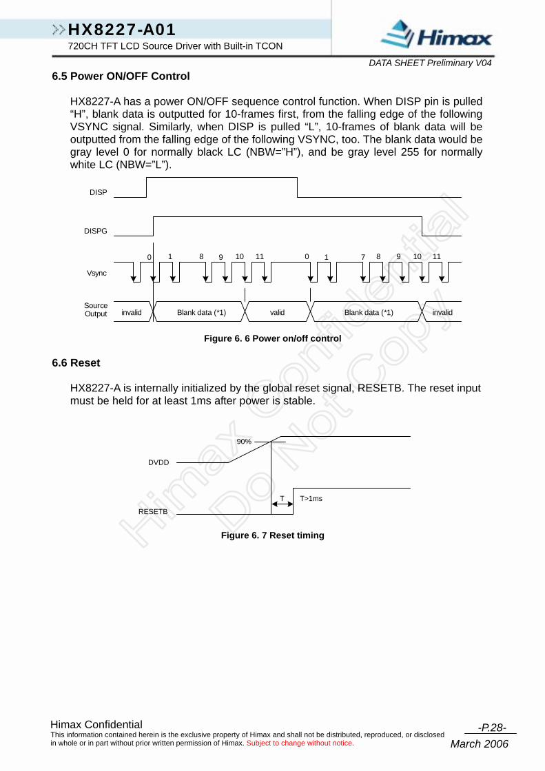
DATA SHEET Preliminary V046.5 Power ON/OFF Control
HX8227-A has a power ON/OFF sequence control function. When DISP pin is pulled “H”, blank data is outputted for 10-frames first, from the falling edge of the following VSYNC signal. Similarly, when DISP is pulled “L”, 10-frames of blank data will be outputted from the falling edge of the following VSYNC, too. The blank data would be gray level 0 for normally black LC (NBW=”H”), and be gray level 255 for normally white LC (NBW=”L”).
DISP
DISPG
Vsync
SourceOutput invalid Blank data (*1) valid Blank data (*1) invalid
10 8 9 10 11 0 1 8 9 10 117
Figure 6. 6 Power on/off control 6.6 Reset
HX8227-A is internally initialized by the global reset signal, RESETB. The reset input must be held for at least 1ms after power is stable.
T T>1ms
90%
DVDD
RESETB
Figure 6. 7 Reset timing

-P.29- Himax Confidential
March 2006 This information contained herein is the exclusive property of Himax and shall not be distributed, reproduced, or disclosed in whole or in part without prior written permission of Himax. Subject to change without notice.
HX8227-A01 720CH TFT LCD Source Driver with Built-in TCON
DATA SHEET Preliminary V04
7. DC Characteristics 7.1 Absolute maximum ratings
Parameter Symbol Rating Unit Logic power supply DVDD -0.3 to 6.0 V Driver power supply AVDD -0.3 to 6.0 V Logic input voltage VI1 -0.3 to DVDD +0.3 V Driver input voltage VI2 -0.3 to AVDD +0.3 V Logic output voltage VO1 -0.3 to DVDD +0.3 V Driver output voltage VO2 -0.3 to AVDD +0.3 V Operation ambient temperature TA -30 to 85 V Storage temperature TSTG -40 to 125 ºC
7.2 Recommended operating conditions (TA =25ºC, DVSS=AVSS=0V)
Parameter Symbol Min. Typ. Max. Unit Logic power supply DVDD 2.25 2.5 3.6 V Driver power supply AVDD 4.8 5.0 5.2 V Input high voltage VIH 0.7*DVDD - DVDD V Input low voltage VIL 0 - 0.3*DVDD V Driver output voltage VO 0.2 - AVDD-0.2 V Gamma voltage VN 0.2 - AVDD-0.2 V Clock frequency fCLK
*1 - 9 15 *1 MHz Note:
1. For parallel RGB interface, maximum clock frequency is 15MHz. For serial RGB interface, the maximum clock frequency is 33MHz.

-P.30- Himax Confidential
March 2006 This information contained herein is the exclusive property of Himax and shall not be distributed, reproduced, or disclosed in whole or in part without prior written permission of Himax. Subject to change without notice.
HX8227-A01 720CH TFT LCD Source Driver with Built-in TCON
DATA SHEET Preliminary V047.3 Electrical Characteristics
(TA =25ºC, DVDD=2.25V to 3.6V, AVDD=4.8V to 5.2V, DVSS=AVSS=0V) Parameter Symbol Condition Min. Typ. Max. Unit
Input low leakage current IIL
No pull-up or pull-down -1 - 1 µA
Input high leakage current IIH No pull-up or
pull-down -1 - 1 µA
Output low voltage VOL *1 IOL=1mA DVSS - DVSS+0.4 V
Output high voltage VOH *1 IOH=-1mA DVDD-0.4 - DVDD V
Gamma resistor RGMA AVDD=5V, TA
=25ºC, V0 to Vn=4V
- 17.1 - kΩ
IVOL AVDD=5V, VO=0.2V, VIN=0.7V
- - (80) µA
Driver output current
IVOH AVDD=5V, VO=4.8V, VIN=4.3V
(80) - - µA
Average output deviation (chip to chip) ΔVd Center gary level - - 10 mV
Output deviation ΔVO1 VO=1.5V to AVDD-1.5V - (±10) (±15) mV
Output deviation ΔVO2 VO < 1.5V or >AVDD-1.5V - (±20) (±40) mV
Logic dynamic current IDD1 DVDD - (1.0)*2 (2.0)*3 mADriver dynamic current IDD2 AVDD - 8.75*4 10*5 mAInput pull up/down resistance RI
VIL= 0V or VIH= DVDD 150 - - kΩ
Note: 1. CKV, STV, OEV pins 2. Parallel interface, fCLK=9MHz, fSTB=17.14KHz, dot inversion pattern, DVDD=2.5V, TA=25ºC 3. Parallel interface, fCLK=9MHz, fSTB=17.14KHz, dot inversion pattern, DVDD=2.75V, TA=-30 to 85ºC 4. Parallel interface, fCLK=9MHz, fSTB=17.14KHz, all white (NBW=”H”) pattern, AVDD=5V, V0=4.5V,
Vn=0.2V, TA=25ºC 5. Parallel interface, fCLK=9MHz, fSTB=17.14KHz, all white (NBW=”H”) pattern, AVDD=5.2V, V0=4.5V,
Vn=0.2V, TA=-30 to 85ºC

-P.31- Himax Confidential
March 2006 This information contained herein is the exclusive property of Himax and shall not be distributed, reproduced, or disclosed in whole or in part without prior written permission of Himax. Subject to change without notice.
HX8227-A01 720CH TFT LCD Source Driver with Built-in TCON
DATA SHEET Preliminary V04
8. AC Characteristics 8.1 Switching characteristics
(TA =25ºC, DVDD=2.25V to 3.6V, AVDD=4.8V to 5.2V, DVSS=AVSS=0V) PARAMETER Symbol Min. Typ. Max. Unit
Logic output delay time TPLH1 *1 - - 50 ns
TPLH2 *2 - - (10) µs
TPLH3 *3 - - (12) µs
TPHL2 *2 - - (10) µs Driver output delay time
TPHL3 *3 - - (12) µs
Input Capacitance CI1 - - 10 pF Note:
1. CLK edge to CKV, STV, OEV and COMSIG pins, CL = 15pF 2. Specified when driver voltage reaches 10% or 90% of the target level. RL=17 kΩ, CL=40pF,
DVDD=2.5V, AVDD=5V. 3. Specified when driver voltage reaches 6-bit accuracy of the target level. RL=17 kΩ, CL=40pF,
DVDD=2.5V, AVDD=5V.

-P.32- Himax Confidential
March 2006 This information contained herein is the exclusive property of Himax and shall not be distributed, reproduced, or disclosed in whole or in part without prior written permission of Himax. Subject to change without notice.
HX8227-A01 720CH TFT LCD Source Driver with Built-in TCON
DATA SHEET Preliminary V048.2 Timing Requirement 1
(480RGBx272, TA =25ºC, DVDD=2.25V to 3.6V, DVSS= 0V) PARAMETER Symbol Min. Typ. Max. Unit
Clock cycle 1/tC *1 - 9 15 MHz
Hsync cycle 1/fH - 17.14 - KHz Vsync cycle 1/fV - 59.94 - Hz Horizontal Signal Horizontal cycle th *2 - 525 - CLK Horizontal display period thd - 480 - CLK Horizontal front porch thf 2 - - CLK Horizontal pulse width thp 2 41 - CLK Horizontal back porch thb 2 2 - CLK Vertical Signal Vertical cycle tv - 286 - H Vertical display period tvd - 272 - H Vertical front porch tvf 1 2 - H Vertical pulse width tvp 1 10 - H Vertical back porch tvb 1 2 - H
Note: 1. Parallel interface. Clock frequency and horizontal signal parameters are tripled in serial interface.
The Maximum clock frequency of serial interface is 33MHz 2. thd=480CLK, thf=2CLK, thp=41CLK, thb=2CLK, thf + fhp + ftb > 44
(480RGBx240, TA =25ºC, DVDD=2.25V to 3.6V, DVSS= 0V) PARAMETER Symbol Min. Typ. Max. Unit
Clock cycle 1/tC *1 - 9.6 15 MHz
Hsync cycle 1/fH - 15.72 - KHz Vsync cycle 1/fV - 60 - Hz Horizontal Signal Horizontal cycle th *2 - 612 - CLK Horizontal display period thd - 480 - CLK Horizontal front porch thf 2 30 - CLK Horizontal pulse width thp 2 46 - CLK Horizontal back porch thb 2 56 - CLK Vertical Signal Vertical cycle tv *3 - 262 - H Vertical display period tvd - 240 - H Vertical front porch tvf 1 4 - H Vertical pulse width tvp 1 3 - H Vertical back porch tvb 1 15 - H
Note: 1. Parallel interface. Clock frequency and horizontal signal parameters are tripled in serial interface.
The Maximum clock frequency of serial interface is 33MHz 2. thd=480CLK, thf=30CLK, thp=46CLK, thb=56CLK, thf + fhp + ftb > 44 3. Values in the table are for NTSC mode. For PAL mode, typical values are tv=312H, tvd=280H,
tvf=6H, tvp=3H, tvb=23H

-P.33- Himax Confidential
March 2006 This information contained herein is the exclusive property of Himax and shall not be distributed, reproduced, or disclosed in whole or in part without prior written permission of Himax. Subject to change without notice.
HX8227-A01 720CH TFT LCD Source Driver with Built-in TCON
DATA SHEET Preliminary V04
(240RGBx320, TA =25ºC, DVDD=2.25V to 3.6V, DVSS= 0V) PARAMETER Symbol Min. Typ. Max. Unit
Clock cycle 1/tC *1 - 5.5 15 MHz Hsync cycle 1/fH - 19.56 - KHz Vsync cycle 1/fV - 60 - Hz Horizontal Signal Horizontal cycle th *2 - 280 - CLK Horizontal display period thd - 240 - CLK Horizontal front porch thf 2 23 - CLK Horizontal pulse width thp 2 10 - CLK Horizontal back porch thb 2 7 - CLK Vertical Signal Vertical cycle tv - 326 - H Vertical display period tvd - 320 - H Vertical front porch tvf 1 2 - H Vertical pulse width tvp 1 2 - H Vertical back porch tvb 1 2 - H
Note: 1. Parallel interface. Clock frequency and horizontal signal parameters are tripled in serial interface.
The Maximum clock frequency of serial interface is 33MHz 2. thd=240CLK, thf=23CLK, thp=10CLK, thb=7CLK, thf + fhp + ftb > 22
(240RGBx240, TA =25ºC, DVDD=2.25V to 3.6V, DVSS= 0V)
PARAMETER Symbol Min. Typ. Max. Unit Clock cycle 1/tC *1 - 4.8 15 MHz Hsync cycle 1/fH - 15.72 - KHz Vsync cycle 1/fV - 60 - Hz Horizontal Signal Horizontal cycle th *2 - 306 - CLK Horizontal display period thd - 240 - CLK Horizontal front porch thf 2 15 - CLK Horizontal pulse width thp 2 23 - CLK Horizontal back porch thb 2 28 - CLK Vertical Signal Vertical cycle tv *3 - 262 - H Vertical display period tvd - 240 - H Vertical front porch tvf 1 4 - H Vertical pulse width tvp 1 3 - H Vertical back porch tvb 1 15 - H
Note: 1. Parallel interface. Clock frequency and horizontal signal parameters are tripled in serial interface.
The Maximum clock frequency of serial interface is 33MHz 2. thd=240CLK, thf=15CLK, thp=23CLK, thb=28CLK, thf + fhp + ftb > 22 3. Values in the table are for NTSC mode. For PAL mode, typical values are tv=312H, tvd=280H,
tvf=6H, tvp=3H, tvb=23H

-P.34- Himax Confidential
March 2006 This information contained herein is the exclusive property of Himax and shall not be distributed, reproduced, or disclosed in whole or in part without prior written permission of Himax. Subject to change without notice.
HX8227-A01 720CH TFT LCD Source Driver with Built-in TCON
DATA SHEET Preliminary V04
tv
tvp tvb tvd tvf
1HVsync
Hsync
DE
Hsync
DE
Dn7-Dn0
Hsync
CLK
DE
Dn7-Dn0
invalid 1st line 2nd line 3rd line last line invalid
th
thp thb
1/tc
thd thf
invalid
1st pixel last pixel2nd pixel
invalid
Figure 8. 1 Input timing

-P.35- Himax Confidential
March 2006 This information contained herein is the exclusive property of Himax and shall not be distributed, reproduced, or disclosed in whole or in part without prior written permission of Himax. Subject to change without notice.
HX8227-A01 720CH TFT LCD Source Driver with Built-in TCON
DATA SHEET Preliminary V048.3 Timing Requirement 2
(TA =25ºC, DVDD=2.25V to 3.6V, DVSS= 0V, tr=tf=2ns) PARAMETER Symbol Min. Typ. Max. Unit
DISP setup time tdiss 10 - - ns
DISP hold time tdish 10 - - ns Clock period PWCLK
*1 66.7 - - ns Clock pulse high period PWH
*1 26.7 - - ns Clock pulse low period PWL
*1 26.7 - - ns Hsync setup time ths 10 - - ns Hsync hold time thh 10 - - ns Data setup time tds 10 - - ns Data hold time tdh 10 - - ns DE setup time tdes 10 - - ns DE hold time tdeh 10 - - ns Vsync setup time tvhs 10 - - ns Vsync hold time tvhh 10 - - ns
Note: 1. For parallel interface, maximum clock frequency is 15MHz. 2. tr, tf is defined 10% to 90% of signal amplitude.
Vsync
0.7DVDD
0.7DVDD
tdiss0.7DVDD
0.7DVDD
tdish
DISP
Vsync 0.3DVDD
tvhs
0.7DVDD 0.7DVDD
0.3DVDDtvhh
CLK
Hsync 0.3DVDD
0.7DVDDCLK
0.3DVDD
0.3DVDD
CLK
Dn7-Dn0
DE0.7DVDD
tf tr
invalid0.7DVDD0.3DVDD
0.7DVDD
tds
0.3DVDD
tdf
invalid
tdes
PWL CLKPWH PWL
tdeh
Hsync
Figure 8. 2 Input setup timing

-P.36- Himax Confidential
March 2006 This information contained herein is the exclusive property of Himax and shall not be distributed, reproduced, or disclosed in whole or in part without prior written permission of Himax. Subject to change without notice.
HX8227-A01 720CH TFT LCD Source Driver with Built-in TCON
DATA SHEET Preliminary V04
9. Ordering Information
Part NO. Package HX8227-A010PDxxx PD : mean COG
xxx : mean chip thickness (µm) , (default 400 µm)
10. Revision History
Version EFF.DATE DESCRIPTION OF CHANGES 2005/03/28 New setup 2005/04/08
1. Add new resolutions: 240RGBx320 and 240RGBx240
2. Add new pin RES2 to select new extra resolution
2005/04/26 1. Update: PAD location table 2. Update: Section 6.3 timing
2005/06/08 1. Update: AC spec about serial RGB interface
2. Update: DC spec max VDD 2.75V 3. Update: Charge pump clock optional
function 4. Update: MS and LR optional function
01
2005/07/12 1. Update : Block Diagram(P.2) 2. Update : PAD location table(P.5) 3. Update : Driver dynamic current
value(P.30) 2005/07/29 1. Update : PAD location table(P.5) 2005/10/26 1. Modify figure 8.1 input timing
2. Modify figure 8.2 input setup timing 02
2005/11/07 1. Modify figure 6. 8 power on/off control 2005/12/09 1. Modify Pad layout coordinate NO. 6, 7,
50, 56, 81, and 87 x pitch 2005/12/16 1. Page 15 pin CLK_TRIG description
modifies (CLKIN to CLK.) 2. Modify figure 8. 3 Thd
2006/02/08 1. Update: DC spec max VDD 3.6V
03
2006/02/20 1. Adding driver dynamic current in page 302. Modify Fig. 4.1 pad location
04
2006/03/15 1. Modify for new part HX8227-A01 2. Modify pin description TEST_IO1 and
TEST_IO3(P.16) 3. Modify Ladder resistors ratio and Input
data and output voltage(P.22~P.26)