hx8347-d ds t v02 090324 - rockbox · data sheet ( doc no. hx8347 -d(t) -ds ) hx8347-d(t) 240rgb x...
TRANSCRIPT

DATA SHEET
( DOC No. HX8347-D(T)-DS )
HX8347-D(T) 240RGB x 320 dot, 262K color, with internal GRAM, TFT Mobile Single Chip Driver Version 02 March, 2009
-P.1- Himax Confidential This information contained herein is the exclusive property of Himax and shall not be distributed, reproduced, or disclosed in whole or in part without prior written permission of Himax. March, 2009
1. General Description ................................ ................................................................................................. 9 2. Features........................................... ........................................................................................................ 10 3. Block Diagram ...................................... .................................................................................................. 12 4. Pin Description .................................... ................................................................................................... 13
4.1 Pin description ............................................................................................................................... 13 4.2 Pin assignment .............................................................................................................................. 16 4.3 PAD coordinates ............................................................................................................................ 17 4.4 Alignment mark.............................................................................................................................. 23 4.5 Bump size ...................................................................................................................................... 24
5. Interface.......................................... ......................................................................................................... 25 5.1 System interface circuit ................................................................................................................. 26
5.1.1 Parallel bus system interface................................................................................................ 27 5.1.2 MCU data color coding ......................................................................................................... 29 5.1.3 Serial bus system interface .................................................................................................. 42
5.2 RGB Interface................................................................................................................................ 45 5.2.1 Color order on RGB interface............................................................................................... 49 5.2.2 RGB data color coding ......................................................................................................... 50
6. Display Data GRAM .................................. .............................................................................................. 53 6.1 Display data GRAM mapping ........................................................................................................ 53 6.2 Address Counter (AC) of GRAM ................................................................................................... 54
6.2.1 System interface to GRAM write direction............................................................................ 55 6.3 GRAM to display address mapping............................................................................................... 60
6.3.1 Normal display on or partial mode on, vertical scroll off....................................................... 62 6.3.2 Vertical scroll display mode .................................................................................................. 64 6.3.3 Updating order on display active area in RGB interface mode ............................................ 67
7. Functional Description ............................. ............................................................................................. 70 7.1 Internal oscillator ........................................................................................................................... 70 7.2 Gamma characteristic correction function ..................................................................................... 71 7.3 Tearing effect output line ............................................................................................................... 91
7.3.1 Tearing effect line modes...................................................................................................... 91 7.3.2 Tearing effect line timing....................................................................................................... 92 7.3.3 Example 1: MPU write is faster than panel read .................................................................. 93 7.3.4 Example 2: MPU write is slower than panel read................................................................. 94
7.4 Content Adaptive Brightness Control (CABC) function ................................................................. 95 7.4.1 Module architectures ............................................................................................................ 96 7.4.2 Brightness control block ....................................................................................................... 97 7.4.3 Minimum brightness setting of CABC function ..................................................................... 98 7.4.4 Display dimming ................................................................................................................... 98
7.5 LCD power generation circuit ........................................................................................................ 99 7.5.1 Power supply circuit.............................................................................................................. 99 7.5.2 LCD power generation scheme.......................................................................................... 101
7.6 Scan Mode Setting ...................................................................................................................... 102 7.7 Power on/off sequence................................................................................................................ 103 7.8 Input/output pin state ................................................................................................................... 107
7.8.1 Output pins ......................................................................................................................... 107 7.8.2 Input pins ............................................................................................................................ 107
8. Command ............................................ .................................................................................................. 108 8.1 Command set .............................................................................................................................. 109 8.2 Index register ................................................................................................................................113 8.3 Himax ID register (PAGE0 - R00h)...............................................................................................113 8.4 Display mode control register (PAGE0 -01h) ...............................................................................113 8.5 Column address start register (PAGE0 -02~03h).........................................................................114 8.6 Column address end register (PAGE0 -04~05h)..........................................................................115 8.7 Row address start register (PAGE0 -06~07h) ..............................................................................115
HX8347-D(T) 240RGB x 320 dot, 262K color, with internal GRAM, TFT Mobile Single Chip Driver List of Contents
March, 2009

-P.2- Himax Confidential
March, 2009
This information contained herein is the exclusive property of Himax and shall not be distributed, reproduced, or disclosed in whole or in part without prior written permission of Himax.
8.8 Row address end register (PAGE0 -08~09h) ...............................................................................115 8.9 Partial area start row register (PAGE0 -0A~0Bh) .........................................................................116 8.10 Partial area end row register (PAGE0 -0C~0Dh)..........................................................................116 8.11 Vertical scroll top fixed area register (PAGE0 -0E~0Fh) ..............................................................118 8.12 Vertical scroll height area register (PAGE0 -10~11h) ...................................................................118 8.13 Vertical scroll button fixed area register (PAGE0 -12~13h)..........................................................118 8.14 Vertical scroll start address register (PAGE0 -14~15h) ............................................................... 120 8.15 Memory access control register (PAGE0 -16h) ........................................................................... 121 8.16 COLMOD control register (PAGE0 -17h)..................................................................................... 122 8.17 OSC control register (PAGE0 -18h & R19h) ............................................................................... 123 8.18 Power control 1 register (PAGE0 -1Ah)....................................................................................... 124 8.19 Power control 2 register (PAGE0 -1Bh)....................................................................................... 125 8.20 Power control 3 register (PAGE0 -1Ch)....................................................................................... 126 8.21 Power control 4 register (PAGE0 -1Dh)....................................................................................... 126 8.22 Power control 5 register (PAGE0 -1Eh)....................................................................................... 127 8.23 Power control 6 register (PAGE0 -1Fh) ....................................................................................... 127 8.24 Read data register (PAGE0 -22h)................................................................................................ 129 8.25 VCOM control 1~3 register (PAGE0 -23~25h) ............................................................................ 130 8.26 Display control 1 register (PAGE0 -26h~R28h)........................................................................... 133 8.27 Frame control register (PAGE0 -29h~R2Ch)............................................................................... 136 8.28 Cycle control register (PAGE0 -2Dh~R2Eh)................................................................................ 138 8.29 Display inversion register (PAGE0 -2Fh)..................................................................................... 139 8.30 RGB interface control register (PAGE0 -31h~R34h) ................................................................... 140 8.31 Panel characteristic control register (PAGE0 -36h)..................................................................... 142 8.32 OTP register (PAGE0 -38h ~ R3Ah)............................................................................................ 143 8.33 CABC control 1~4 register (PAGE0 -3Ch~3Fh) .......................................................................... 144 8.34 Gamma control 1~35 register (PAGE0 -40h~5Dh)...................................................................... 146 8.35 Mode control register (PAGE0 -60h) ........................................................................................... 151 8.36 ID Register (PAGE0 -R61h~R63h).............................................................................................. 151 8.37 Power saving internal control register (PAGE0 -RE4h~RE7h).................................................... 152 8.38 Source OP control (PAGE0 -RE8h~E9h) .................................................................................... 153 8.39 Power control internal used (PAGE0 -REAh~ECh) ..................................................................... 154 8.40 Command page select register (RFFh) ....................................................................................... 154 8.41 CABC control 5~7 register (PAGE1 – RC3h, RC5h, RC7h)........................................................ 155 8.42 Gain select register 0~8 (PAGE1 – RCBh~D3h)......................................................................... 156
9. Layout Recommendation .............................. ...................................................................................... 158 10. OTP Programming.................................... ............................................................................................ 160
10.1 OTP programming flow................................................................................................................ 160 11. Electrical Characteristic .......................... ............................................................................................ 163
11.1 Absolute maximum ratings .......................................................................................................... 163 11.2 ESD protection level .................................................................................................................... 163 11.3 Maximum layout resistance ......................................................................................................... 164 11.4 DC characteristics ....................................................................................................................... 165
11.4.1 Current consumption .......................................................................................................... 167 11.5 AC Characteristics....................................................................................................................... 168
11.5.1 Parallel interface characteristics (8080-series MPU) ......................................................... 168 11.5.2 Serial Interface Characteristics .......................................................................................... 170 11.5.3 RGB interface characteristics............................................................................................. 171 11.5.4 Reset input timing............................................................................................................... 173
12. Ordering Information............................... ............................................................................................. 174 13. Revision History ................................... ................................................................................................ 174
HX8347-D(T) 240RGB x 320 dot, 262K color, with internal GRAM, TFT Mobile Single Chip Driver List of Contents
March, 2009

-P.3- Himax Confidential
March, 2009
This information contained herein is the exclusive property of Himax and shall not be distributed, reproduced, or disclosed in whole or in part without prior written permission of Himax.
Figure 5.1 Register read/write timing in parallel bus system interface (for I80 series MPU) ............ 27 Figure 5.2 GRAM read/write timing in parallel bus system interface (for I80 series MPU)............... 28 Figure 5.3 Example of I80- system 18-bit parallel bus interface....................................................... 31 Figure 5.4 Input data bus and GRAM data mapping in 18-bit bus system interface with 18-bit-data
Input (“IM3, IM2, IM1, IM”=”1010” or “1000”) ............................................................................. 31 Figure 5.5 Example of I80 system 16-bit parallel bus interface type I .............................................. 32 Figure 5.6 Example of I80 system 16-bit parallel bus interface type II ............................................. 32 Figure 5.7 Input data bus and GRAM data mapping in 16-bit bus system interface with 12-bit-data
input (R17H=03h and “IM3, IM2, IM1, IM0”=”0000”) ................................................................. 33 Figure 5.8 Input data bus and GRAM data mapping in 16-bit bus system interface with 16-bit-data
input (R17H=05h and “IM3, IM2, IM1, IM0”=”0000”) ................................................................. 33 Figure 5.9 Input data bus and GRAM data mapping in 16-bit bus system interface with 18 bit-data
input (R17H=06h and “IM3, IM2, IM1, IM0”=”0000”) ................................................................. 33 Figure 5.10 Input data bus and GRAM data mapping in 16-bit bus system interface with 18(16+2)
bit-data input (R17H=07h and “IM3, IM2, IM1, IM0”=”0000”) .................................................... 33 Figure 5.11 Input data bus and GRAM data mapping in 16-bit bus system interface with 12-bit-data
input (R17H=03h and “IM3, IM2, IM1, IM0”=”0010”) ................................................................. 34 Figure 5.12 Input data bus and GRAM data mapping in 16-bit bus system interface with 16-bit-data
input (R17H=05h and “IM3, IM2, IM1, IM0”=”0010”) ................................................................. 34 Figure 5.13 Input data bus and GRAM data mapping in 16-bit bus system interface with 18(12+6)
bit-data input (R17H=06h and “IM3, IM2, IM1, IM0”=”0010”) .................................................... 34 Figure 5.14 Input data bus and GRAM data mapping in 16-bit bus system interface with 18(16+2)
bit-data input (R17H=07h and “IM3, IM2, IM1, IM0”=”0010”) .................................................... 34 Figure 5.15 Example of I80 system 9-bit parallel bus interface type I .............................................. 35 Figure 5.16 Example of I80 system 9-bit parallel bus interface type II ............................................. 35 Figure 5.17 Input data bus and GRAM data mapping in 9-bit bus system interface with 18-bit-data
input (R17H=06h and “IM3, IM2, IM1, IM0”=”1001”) ................................................................. 36 Figure 5.18 Input data bus and GRAM data mapping in 9-bit bus system interface with 18-bit-data
input (R17H=06h and “IM3, IM2, IM1, IM0”=”1011”).................................................................. 36 Figure 5.19 Example of I80 system 8-bit parallel bus interface type I .............................................. 37 Figure 5.20 Example of I80 system 8-bit parallel bus interface type II ............................................. 37 Figure 5.21 Input data bus and GRAM data mapping in 8-bit bus system interface with 12-bit-data
input (R17H=03h and“IM3, IM2, IM1, IM0”=”0001”) .................................................................. 38 Figure 5.22 Input data bus and GRAM data mapping in 8-bit bus system interface with 16-bit-data
input (R17H=05h and “IM3, IM2, IM1, IM0”=”0001”) ................................................................. 38 Figure 5.23 Input data bus and GRAM data mapping in 8-bit bus system interface with 18-bit-data
input (R17H=06h and “IM3, IM2, IM1, IM0”=”0001”) ................................................................. 38 Figure 5.24 Input data bus and GRAM data mapping in 8-bit bus system interface with 12-bit-data
input (R17H=03h and“IM3, IM2, IM1, IM0”=”0011”)................................................................... 39 Figure 5.25 Input data bus and GRAM data mapping in 8-bit bus system interface with 16-bit-data
input (R17H=05h and “IM3, IM2, IM1, IM0”=”0011”).................................................................. 39 Figure 5.26 Input data bus and GRAM data mapping in 8-bit bus system interface with 18-bit-data
input (R17H=06h and “IM3, IM2, IM1, IM0”=”0011”).................................................................. 39 Figure 5.27 Index register read/write timing in 3-wire serial bus system interface ........................... 42 Figure 5.28 Data write timing in 3-wire serial bus system interface.................................................. 43 Figure 5.29 Index register write timing in 4-wire serial bus system interface ................................... 44 Figure 5.30 Data write timing in 4-wire serial bus system interface.................................................. 44 Figure 5.31 DOTCLK cycle ............................................................................................................... 45 Figure 5.32 RGB interface circuit input timing diagram .................................................................... 46 Figure 5.33 RGB mode timing diagram ............................................................................................ 47 Figure 5.34 RGB 18-bit/pixel on 6-bit data width .............................................................................. 50 Figure 5.35 RGB 16-bit/pixel on 16-bit data width ............................................................................ 51 Figure 5.36 RGB 18-bit/pixel on 18-bit data width ............................................................................ 52 Figure 6.1 Image data sending order from host................................................................................ 55 Figure 6.2 Image data writing control................................................................................................ 55
HX8347-D(T) 240RGB x 320 dot, 262K color, with internal GRAM, TFT Mobile Single Chip Driver List of Figures
March, 2009

-P.4- Himax Confidential
March, 2009
This information contained herein is the exclusive property of Himax and shall not be distributed, reproduced, or disclosed in whole or in part without prior written permission of Himax.
Figure 6.3 Example for rotation with MY, MX and MV - 1................................................................. 58 Figure 6.4 Example for rotation with MY, MX and MV - 2................................................................. 59 Figure 6. 5 Partial Display Area Setting (ML=’0’) .............................................................................. 63 Figure 6. 6 Partial Display Area Setting (ML=’1’) .............................................................................. 63 Figure 6.7 Vertical scrolling ............................................................................................................... 64 Figure 6.8 Memory map of vertical scrolling 1 .................................................................................. 64 Figure 6.9 Memory map of vertical scrolling 2 .................................................................................. 65 Figure 6.10 Memory map of vertical scrolling 3 ................................................................................ 65 Figure 6.11 Vertical scrolling example............................................................................................... 66 Figure 6.12 Data streaming order in RGB I/F ................................................................................... 67 Figure 6.13 Updating order when MY = ‘0’ and MX = ‘0’ .................................................................. 68 Figure 6.14 Updating order when MY = ‘0’ and MX = ‘1’ .................................................................. 68 Figure 6.15 Updating order when MY = ‘1’ and MX = ‘0’ .................................................................. 69 Figure 6.16 Updating order when MY = ‘1’ and MX = ‘1’ .................................................................. 69 Figure 7.1 HX8347-D internal clock circuit........................................................................................ 70 Figure 7.2 Grayscale control ............................................................................................................. 71 Figure 7.3 Gamma resister stream and gamma reference voltage .................................................. 73 Figure 7.4 Relationship between source output and Vcom .............................................................. 90 Figure 7.5 Relationship between GRAM data and output level (normal white panel REV_Panel=“0”)
................................................................................................................................................... 90 Figure 7.6 TE mode 1 output ............................................................................................................ 91 Figure 7.7 TE mode 2 output ............................................................................................................ 91 Figure 7.8 TE output waveform......................................................................................................... 91 Figure 7.9 Waveform of tearing effect signal .................................................................................... 92 Figure 7.10 Timing of tearing effect signal ........................................................................................ 92 Figure 7.11 Timing of MPU write is faster than panel read ............................................................... 93 Figure 7.12 Display of MPU write is faster than panel read.............................................................. 93 Figure 7.13 Timing of MPU write is slower than panel read.............................................................. 94 Figure 7.14 Display of MPU write is slower than panel read ............................................................ 94 Figure 7.15 Example of CABC function ............................................................................................ 95 Figure 7.16 CABC block diagram...................................................................................................... 95 Figure 7.17 CABC_PWM_OUT output duty...................................................................................... 97 Figure 7.18 Dimming function ........................................................................................................... 98 Figure 7.19 Block diagram of HX8347-D power circuit ..................................................................... 99 Figure 7.20 LCD power generation scheme ................................................................................... 101 Figure 7.21 Gate Scan Mode .......................................................................................................... 102 Figure 7.22 Display on/off set flow .................................................................................................. 103 Figure 7.23 Standby mode setting flow........................................................................................... 104 Figure 7.24 Deep standby mode setting flow.................................................................................. 105 Figure 7.25 Power supply setting flow ............................................................................................ 106 Figure 8.1 Index register ..................................................................................................................113 Figure 8.2 Himax ID register (PAGE0 -00h).....................................................................................113 Figure 8.3 Display mode control register (PAGE0 -01h)..................................................................113 Figure 8.4 Column address start register upper byte (PAGE0 -02h)...............................................114 Figure 8.5 Column address start register low byte (PAGE0 -03h)...................................................114 Figure 8.6 Column address end register upper byte (PAGE0 -04h)................................................115 Figure 8.7 Column address end register low byte (PAGE0 -05h)....................................................115 Figure 8.8 Row address start register upper byte (PAGE0 -06h) ....................................................115 Figure 8.9 Row address start register low byte (PAGE0 -07h)........................................................115 Figure 8.10 Row address end register upper byte (PAGE0 -08h) ...................................................115 Figure 8.11 Row address end register low byte (PAGE0 -09h) .......................................................115 Figure 8.12 Partial area start row register upper byte (PAGE0 -0Ah) .............................................116 Figure 8.13 Partial area start row register low byte (PAGE0 -0Bh) .................................................116 Figure 8.14 Partial area end row register upper byte (PAGE0 -0Ch) ..............................................116 Figure 8.15 Partial area end row register low byte (PAGE0 -0Dh) ..................................................116
HX8347-D(T) 240RGB x 320 dot, 262K color, with internal GRAM, TFT Mobile Single Chip Driver List of Figures
March, 2009

-P.5- Himax Confidential
March, 2009
This information contained herein is the exclusive property of Himax and shall not be distributed, reproduced, or disclosed in whole or in part without prior written permission of Himax.
Figure 8.16 Vertical scroll top fixed area register upper byte (PAGE0 -0Eh) ..................................118 Figure 8.17 Vertical scroll top fixed area register low byte (PAGE0 -0Fh) ......................................118 Figure 8.18 Vertical scroll height area register upper byte (PAGE0 -10h).......................................118 Figure 8.19 Vertical scroll height area register low byte (PAGE0 -11h) ..........................................118 Figure 8.20 Vertical scroll button fixed area register upper byte (PAGE0 -12h)..............................118 Figure 8.21 Vertical scroll button fixed area register low byte (PAGE0 -13h) .................................118 Figure 8.22 Vertical scroll start address register upper byte (PAGE0 -14h)................................... 120 Figure 8.23 Vertical scroll start address register low byte (PAGE0 -15h)....................................... 120 Figure 8.24 Memory access control register (PAGE0 -16h) ........................................................... 121 Figure 8.25 COLMOD control register (PAGE0 -17h)..................................................................... 122 Figure 8.26 OSC control 1 register (PAGE0 -18h).......................................................................... 123 Figure 8.27 OSC control 2 register (PAGE0 -19h).......................................................................... 123 Figure 8.28 Power control 1 register (PAGE0 -1Ah)....................................................................... 124 Figure 8.29 Power control 2 register (PAGE0 -1Bh)....................................................................... 125 Figure 8.30 Power control 3 register (PAGE0 -1Ch)....................................................................... 126 Figure 8.31 Power control 4 register (PAGE0 -1Dh)....................................................................... 126 Figure 8.32 Power control 5 register (PAGE0 -1Eh)....................................................................... 127 Figure 8.33 Power control 6 register (PAGE0 -1Fh) ....................................................................... 127 Figure 8.34 Read data register (PAGE0 -22h) ................................................................................ 129 Figure 8.35 Vcom control 1 register (PAGE0 -23h) ........................................................................ 130 Figure 8.36 Vcom control 2 register (PAGE0 -24h) ........................................................................ 130 Figure 8.37 Vcom control 3 register (PAGE0 -25h) ........................................................................ 130 Figure 8.38 Display control 1 register (PAGE0 -26h)...................................................................... 133 Figure 8.39 Display control 2 register (PAGE0 -27h)...................................................................... 133 Figure 8.40 Display control 3 register (PAGE0 -28h)...................................................................... 133 Figure 8.41 Frame control 1 register (PAGE0 -29h) ....................................................................... 136 Figure 8.42 Frame control 2 register (PAGE0 -2Ah)....................................................................... 136 Figure 8.43 Frame control 3 register (PAGE0 -2Bh)....................................................................... 136 Figure 8.44 Frame control 4 register (PAGE0 -2Ch) ...................................................................... 136 Figure 8.45 Cycle control register 1 (PAGE0 -2Dh)........................................................................ 138 Figure 8.46 Cycle control register 2 (PAGE0 -2Eh) ........................................................................ 138 Figure 8.47 Cycle control register (PAGE0 -2Fh) ........................................................................... 139 Figure 8.48 RGB interface control register (PAGE0 -31h).............................................................. 140 Figure 8.49 RGB interface control register (PAGE0 -32h).............................................................. 140 Figure 8.50 RGB interface control register (PAGE0 -33h).............................................................. 140 Figure 8.51 RGB interface control register (PAGE0 -34h).............................................................. 140 Figure 8.52 Panel characteristic control register (PAGE0 -36h)..................................................... 142 Figure 8.53 OTP command 1 (PAGE0 -38h) .................................................................................. 143 Figure 8.54 OTP command 2 (PAGE0 -39h) .................................................................................. 143 Figure 8.55 OTP command 3 (PAGE0 -3Ah).................................................................................. 143 Figure 8.56 CABC control 1 register (PAGE0 -3Ch) ....................................................................... 144 Figure 8.57 CABC control 2 register (PAGE0 -3Dh) ....................................................................... 144 Figure 8.58 CABC control 3 register (PAGE0 -3Eh) ....................................................................... 144 Figure 8.59 CABC control 4 register (PAGE0 -3Fh) ....................................................................... 144 Figure 8.60 Gamma control 1 register (PAGE0 -40h)..................................................................... 146 Figure 8.61 Gamma control 2 register (PAGE0 -41h)..................................................................... 146 Figure 8.62 Gamma control 3 register (PAGE0 -42h)..................................................................... 146 Figure 8.63 Gamma control 4 register (PAGE0 -43h)..................................................................... 146 Figure 8.64 Gamma control 5 register (PAGE0 -44h)..................................................................... 146 Figure 8.65 Gamma control 6 register (PAGE0 -45h)..................................................................... 146 Figure 8.66 Gamma control 7 register (PAGE0 -46h)..................................................................... 147 Figure 8.67 Gamma control 8 register (PAGE0 -47h)..................................................................... 147 Figure 8.68 Gamma control 9 register (PAGE0 -48h)..................................................................... 147 Figure 8.69 Gamma control 10 register (PAGE0 -49h)................................................................... 147 Figure 8.70 Gamma control 11 register (PAGE0 -4Ah)................................................................... 147
HX8347-D(T) 240RGB x 320 dot, 262K color, with internal GRAM, TFT Mobile Single Chip Driver List of Figures
March, 2009
-P.6- Himax Confidential
March, 2009
This information contained herein is the exclusive property of Himax and shall not be distributed, reproduced, or disclosed in whole or in part without prior written permission of Himax.
Figure 8.71 Gamma control 12 register (PAGE0 -4Bh) .................................................................. 147 Figure 8.72 Gamma control 13 register (PAGE0 -4Ch) .................................................................. 148 Figure 8.73 Gamma control 14 register (PAGE0 -50h)................................................................... 148 Figure 8.74 Gamma control 15 register (PAGE0 -51h)................................................................... 148 Figure 8.75 Gamma control 16 register (PAGE0 -52h)................................................................... 148 Figure 8.76 Gamma control 17 register (PAGE0 -53h)................................................................... 148 Figure 8.77 Gamma control 18 register (PAGE0 -54h)................................................................... 148 Figure 8.78 Gamma control 19 register (PAGE0 -55h)................................................................... 149 Figure 8.79 Gamma control 20 register (PAGE0 -56h)................................................................... 149 Figure 8.80 Gamma control 21 register (PAGE0 -57h)................................................................... 149 Figure 8.81 Gamma control 22 register (PAGE0 -58h)................................................................... 149 Figure 8.82 Gamma control 23 register (PAGE0 -59h)................................................................... 149 Figure 8.83 Gamma control 24 register (PAGE0 -5Ah) .................................................................. 150 Figure 8.84 Gamma control 25 register (PAGE0 -5Bh) .................................................................. 150 Figure 8.85 Gamma control 26 register (PAGE0 -5Ch) .................................................................. 150 Figure 8.86 Gamma control 27 register (PAGE0 -5Dh) .................................................................. 150 Figure 8.87 Mode control register (PAGE0 -60h)............................................................................ 151 Figure 8.88 ID1 Register (PAGE0 -61h).......................................................................................... 151 Figure 8.89 ID2 Register (PAGE0 -62h).......................................................................................... 151 Figure 8.90 ID3 Register (PAGE0 -63h).......................................................................................... 151 Figure 8.91 Power saving internal control register (R68h) ............................................................. 152 Figure 8.92 Power saving Internal control register (R69h) ............................................................. 152 Figure 8.93 Power saving Internal control register (R70h) ............................................................. 152 Figure 8.94 Power saving Internal control register (R71h) ............................................................. 152 Figure 8.95 Source OP control register (PAGE0 -RE8h)................................................................ 153 Figure 8.96 Source OP control register (PAGE0 -RE9h)................................................................ 153 Figure 8.97 Power control internal used (1) register (PAGE0 -REAh)............................................ 154 Figure 8.98 Power control internal used (2) register (PAGE0 -REBh)............................................ 154 Figure 8.99 Source control internal used (1) register (PAGE0 -RECh) .......................................... 154 Figure 8.100 Source control internal used (2) register (PAGE0 -REDh) ........................................ 154 Figure 8.101 Command page select register (RFFh) ..................................................................... 154 Figure 8.102 CABC control 5 (PAGE1 – RC3h).............................................................................. 155 Figure 8.103 CABC control 6 (PAGE1 – RC5h).............................................................................. 155 Figure 8.104 CABC control 7 (PAGE1 – RC7h).............................................................................. 155 Figure 8.105 Gain select register 0 (PAGE1 – RCBh) .................................................................... 156 Figure 8.106 Gain select register 1 (PAGE1 – RCCh).................................................................... 156 Figure 8.107 Gain select register 2 (PAGE1 – RCDh).................................................................... 156 Figure 8.108 Gain select register 3 (PAGE1 – RCEh) .................................................................... 156 Figure 8.109 Gain select register 4 (PAGE1 – RCFh) .................................................................... 156 Figure 8.110 Gain select register 5 (PAGE1 – RD0h) .................................................................... 156 Figure 8.111 Gain select register 6 (PAGE1 – RD1h) .................................................................... 156 Figure 8.112 Gain select register 7 (PAGE1 – RD2h) .................................................................... 157 Figure 8.113 Gain select register 8 (PAGE1 – RD3h) .................................................................... 157 Figure 9.1 Layout recommendation of HX8347-D MPU mode ....................................................... 158 Figure 9.2 Layout recommendation of HX8347-D (SPI+RGB) ....................................................... 159 Figure 11.1 Parallel interface characteristics (8080-series MPU) ................................................... 168 Figure 11.2 Chip select timing......................................................................................................... 169 Figure 11.3 Write to read and read to write timing .......................................................................... 169 Figure 11.4 Serial interface characteristics ..................................................................................... 170 Figure 11.5 Reset input timing ........................................................................................................ 173
HX8347-D(T) 240RGB x 320 dot, 262K color, with internal GRAM, TFT Mobile Single Chip Driver List of Figures
March, 2009

-P.7- Himax Confidential
March, 2009
This information contained herein is the exclusive property of Himax and shall not be distributed, reproduced, or disclosed in whole or in part without prior written permission of Himax.
Table 5.1 Input bus format selection of system interface circuit ....................................................... 26 Table 5.2 Data pin function for I80 series CPU ................................................................................. 27 Table 5.3 8-bit parallel interface type I GRAM write table ................................................................. 29 Table 5.4 16-bit parallel interface type I GRAM write table ............................................................... 29 Table 5.5 9-bit parallel interface type I GRAM write table ................................................................. 29 Table 5.6 18-bit parallel interface type I GRAM write table ............................................................... 29 Table 5.7 8-bit parallel interface type II GRAM write table ................................................................ 30 Table 5.8 16-bit parallel interface type II GRAM write set table ........................................................ 30 Table 5.9 9-bit parallel interface set type II GRAM write table .......................................................... 30 Table 5.10 18-bit parallel interface type II GRAM write set table ...................................................... 30 Table 5.11 8-bit parallel interface type I GRAM read table................................................................ 40 Table 5.12 16-bit parallel interface type I GRAM read table ............................................................. 40 Table 5.13 9-bit parallel interface type I GRAM read table ............................................................... 40 Table 5.14 18-bit parallel interface type I GRAM read table ............................................................. 40 Table 5.15 8-bit parallel interface type II GRAM read table .............................................................. 41 Table 5.16 16-bit parallel interface type II GRAM read table ............................................................ 41 Table 5.17 9-bit parallel interface type II GRAM read table .............................................................. 41 Table 5.18 18-bit parallel interface type II GRAM read table ............................................................ 41 Table 5.19 Function of RS and R/W bit bus ...................................................................................... 42 Table 5.20 RGB interface bus width set table ................................................................................... 48 Table 5.21 Meaning of pixel information for main colors on RGB interface...................................... 49 Table 6.1 GRAM address for display panel position ......................................................................... 53 Table 6.2 CASET and PASET control for physical column/page pointers........................................ 55 Table 6.3 Rules for updating GRAM rrder ........................................................................................ 56 Table 6.4 Address direction settings................................................................................................. 57 Table 6.5 GRAM X address and display panel position.................................................................... 60 Table 6.6 GRAM address and display panel position (SMY=L)........................................................ 61 Table 6.7 GRAM address and display panel position (SMY=’H’) ..................................................... 61 Table 6.8 Rules for updating order on display active area in RGB interface display mode ............. 69 Table 7.1 Gamma-adjustment registers............................................................................................ 72 Table 7.2 Offset adjustment 0 ~ 5..................................................................................................... 74 Table 7.3 Center adjustment............................................................................................................. 74 Table 7.4 VinP/N 0 ............................................................................................................................ 75 Table 7.5 VinP/N 1 ............................................................................................................................ 76 Table 7.6 VinP/N 2 ............................................................................................................................ 77 Table 7.7 VinP/N 10 .......................................................................................................................... 78 Table 7.8 VinP/N 11 .......................................................................................................................... 79 Table 7.9 VinP/N 12 .......................................................................................................................... 80 Table 7.10 VinP/N4 ........................................................................................................................... 82 Table 7.11 VinP/N 8 .......................................................................................................................... 84 Table 7.12 VinP/N 3 .......................................................................................................................... 85 Table 7.13 VinP/N 5 .......................................................................................................................... 85 Table 7.14 VinP/N 6 .......................................................................................................................... 86 Table 7.15 VinP/N 7 .......................................................................................................................... 86 Table 7.16 VinP/N 9 .......................................................................................................................... 87 Table 7.17 Voltage calculation formula of 64-grayscale voltage (positive polarity) .......................... 88 Table 7.18 Voltage calculation formula of grayscale voltage V4~V7 and V56~V59......................... 88 Table 7.19 Voltage calculation formula of 64-grayscale voltage (negative polarity) ......................... 89 Table 7.20 Voltage calculation formula of grayscale voltage V59~V56 and V7~V4......................... 89 Table 7.21 AC characteristics of tearing effect signal ....................................................................... 92 Table 7.22 Adoptability of capacitor................................................................................................. 100 Table 7.23 Characteristics of output pins ........................................................................................ 107 Table 7.24 Characteristics of input pins .......................................................................................... 107 Table 8.1 List table of command set page 0..................................................................................... 111 Table 8.2 List table of command set page 1.....................................................................................112
HX8347-D(T) 240RGB x 320 dot, 262K color, with internal GRAM, TFT Mobile Single Chip Driver List of Tables
March, 2009
-P.8- Himax Confidential
March, 2009
This information contained herein is the exclusive property of Himax and shall not be distributed, reproduced, or disclosed in whole or in part without prior written permission of Himax.
Table 11.1 Absolute maximum ratings............................................................................................. 163 Table 11.2 ESD protection level ...................................................................................................... 163 Table 11.3 Current consumption ..................................................................................................... 167
HX8347-D(T) 240RGB x 320 dot, 262K color, with internal GRAM, TFT Mobile Single Chip Driver List of Tables
March, 2009
-P.9- Himax Confidential This information contained herein is the exclusive property of Himax and shall not be distributed, reproduced, or disclosed in whole or in part without prior written permission of Himax. March, 2009
1. General Description This document describes HX8347-D 240RGBx320 dots resolution driving controller. The HX8347-D is designed to provide a single-chip solution that combines a gate driver, a source driver, power supply circuit for 262,144 colors to drive a TFT panel with 240RGBx320 dots at maximum. The HX8347-D can be operated in low-voltage (1.4V) condition for the interface and integrated internal boosters that produce the liquid crystal voltage, breeder resistance and the voltage follower circuit for liquid crystal driver. In addition, The HX8347-D also supports various functions to reduce the power consumption of a LCD system via software control. The HX8347-D supports two interface groups: Command-Parameter interface group, Register-Content interface group. The interface groups are selected by the external pin IFSEL setting. This manual description focuses on Register-Content interface group. About the Command-Parameter interface group, please refer to the HX8347-D (N) datasheet for detail. The HX8347-D is suitable for any small portable battery-driven and long-term driving products, such as small PDAs, digital cellular phones and bi-directional pagers.
HX8347-D(T) 240RGB x 320 dot, 262K color, with internal GRAM, TFT Mobile Single Chip Driver Preliminary Version 01
December, 2008

-P.10- Himax Confidential
March, 2009
This information contained herein is the exclusive property of Himax and shall not be distributed, reproduced, or disclosed in whole or in part without prior written permission of Himax.
HX8347-D(T) 240RGB x 320 dot, 262K color, TFT Mobile Single Chip Driver DATA SHEET Preliminary V01
2. Features
Single chip solution to drive a a-TFT LCD panel Display Resolution: 240(H) x RGB(H) x 320(V) Display Color modes
Normal Display Mode On 1. System Interface Circuit
a. 4096(R (4), G (4), B (4)) colors b. 65, 536(R (5), G (6), B (5)) colors c. 262, 144(R (6), G (6), B (6)) colors
2. RGB Interface Circuit a. 65,536(R(5),G(6),B(5)) colors b. 262,144(R(6),G(6),B(6)) colors
Idle Mode On 1. 8 (R (1), G (1), B (1)) colors.
Outputs Source outputs: 720 source lines Selectable gate line control signal for glass 320 gate lines Adjusted source voltages (V0p ~V63p, V0n ~V63n)
Display interface:
System interface: a. 8-/9-/16-/18-bit parallel bus system interface b. 3-/4-wire serial bus system interface
RGB interface: a. 6-/16-/18-bit RGB interface
Internal graphics RAM capacity: 240 x18x320 bit = 1382400bits
Display features
The vertical scroll display function in line units Partial area display mode. Software programmable color depth mode
On chip
OTP memory to store initialization register settings Automatic malfunction recovery for default values Internal oscillator and hardware reset function DC/DC converter and charge bump circuit for source, glass gate driving
voltage Adjust AC VCOM generation

-P.11- Himax Confidential
March, 2009
This information contained herein is the exclusive property of Himax and shall not be distributed, reproduced, or disclosed in whole or in part without prior written permission of Himax.
HX8347-D(T) 240RGB x 320 dot, 262K color, TFT Mobile Single Chip Driver DATA SHEET Preliminary V01
LCD Driving Inversion Algorithm Frame inversion AC liquid-crystal drive 1~7 line inversion AC liquid-crystal drive
Input power supply
IOVCC = 1.65 to 3.3V (Logic IO power supply voltage range) VCI = 2.3 to 3.3V (Driver power supply voltage range)
Output voltage levels
DDVDH = 5.0 V for two time pump (Power supply for driver circuit range) DDVDH = 6.1 V for three time pump (Power supply for driver circuit range) VREG1 = 3.3V to 5.8V (Source output voltage range) VGH = +9.0 to +16.5V (Positive Gate output voltage range) VGL = -6.0 to -13.5V (Negative Gate output voltage range) VCOMH = 2.5V to 5.8V, 15mv/step (Common electrode output high voltage) VCOML = -2.5V to 0.0V, 15mv/step (Common electrode output low voltage)
Supply CABC function Low power consumption, suitable for battery operated systems CMOS compatible inputs Chip on Glass Operating temperature range : -40 ~ 85

-P.12- Himax Confidential
March, 2009
This information contained herein is the exclusive property of Himax and shall not be distributed, reproduced, or disclosed in whole or in part without prior written permission of Himax.
HX8347-D(T) 240RGB x 320 dot, 262K color, TFT Mobile Single Chip Driver DATA SHEET Preliminary V01
3. Block Diagram
NCS MPU IF
Serial IF
Gate
Driver
Grayscale voltage
generatorVTEST
VMONI
Gamma adjusting circuit
Source
driver
D/A Converter
circuit
Data Latch
C11P/C
11N
S1 ~ S720
Internal
registerOTP
GRAM control
GRAM
TimingControl
Step Up1
CABC
Step Up2 Step Up3
C12P/C12N
DDVDH
C21P/C
21N
C22P/C
22N
VGH
VGL
C31P/C
31N
VCL
VCOM Cricuit
VCOM
NRD
NWR_SCL
DNC_SCL
V0~63
G1~G320
VGH/VGL
RCM1~0,
IM3~IM0
IFSEL
NRESET
DE
VSYNC
HSYNC
2TEST 2~1
TEST10 ~38
7
VSSD
VSSA
Generator Timing
RC
OSC
OSC
Power
RegulatorVDDD
18DB17~0
DOTCLK
18-bit
16-bit
8-bit
9-bit
SDA
MPU IF Serial IF
RGB IF 18-bit
16-bit
6-bit
CABC_PWM_OUT

-P.13- Himax Confidential
March, 2009
This information contained herein is the exclusive property of Himax and shall not be distributed, reproduced, or disclosed in whole or in part without prior written permission of Himax.
HX8347-D(T) 240RGB x 320 dot, 262K color, TFT Mobile Single Chip Driver DATA SHEET Preliminary V01
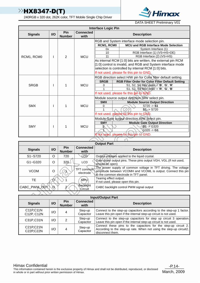
4. Pin Description 4.1 Pin description
Interface Logic Pin
Signals I/O Pin Number
Connected with Description
IFSEL I 1 MPU
Interface format select pin IFSEL Interface Format Selection
0 Register-content interface mode 1 Command-Parameter interface mode
In this document, the IFSEL has to be connected to GND and Register-Content interface mode is select.
IM3, IM2,IM1,IM0 I 4 VSSD/ IOVCC
System interface select. IM3 IM2 IM1 IM0 Interface
0 0 0 0 8080 MCU 16-bit Parallel type I 0 0 0 1 8080 MCU 8-bit Parallel type I 0 0 1 0 8080 MCU 16-bit Parallel type II 0 0 1 1 8080 MCU 8-bit Parallel type II 0 1 0 ID 3-wire serial interface 0 1 1 - 4-wire serial interface 1 0 0 0 8080 MCU 18-bit parallel type I 1 0 0 1 8080 MCU 9-bit parallel type I 1 0 1 0 8080 MCU 18-bit parallel type II 1 0 1 1 8080 MCU 9-bit parallel type II
If not used, please fix this pin to IOVCC or VSSD level.
NCS I 1 MPU
Chip select signal. Low: chip can be accessed; High: chip cannot be accessed. Must be connected to VSSD if not in use.
NWR_SCL I 1 MPU
(NWR) Write enable pin I80 parallel bus system interface. (SCL) server as serial data clock in serial bus system interface when IFSEL=0. Fix it to IOVCC or VSSD level when not used.
NRD I 1 MPU (NRD) Read enable pin I80 parallel bus system interface. If not used, please fix this pin at IOVCC or GND level
SDA I/O 1 MCU Serial data input pin and output pin in serial bus system interface. The data is inputted on the rising edge of the SCL signal. If not used, please let it open
DNC_SCL I 1 MPU
(DNC) Command / parameter or display data selection pin. (SCL) server as serial data clock in serial bus system interface when IFSEL=1. If not used, please fix this pin at IOVCC or GND level.
VSYNC I 1 MPU Vertical synchronizing signal in RGB interface. Has to be fixed to VSSD level if it is not used.
HSYNC I 1 MPU Horizontal synchronizing signal in RGB interface. Has to be fixed to VSSD level if it is not used.
DE I 1 MPU A data ENABLE signal in RGB I/F mode. Has to be fixed to VSSD level if it is not used.
DOTCLK I 1 MPU Data enable signal in RGB interface. Has to be fixed to VSSD level if it is not used.
NRESET I 1 MPU or
reset circuit Reset pin. Setting either pin low initializes the LSI. Must be reset after power is supplied.
DB17~0 I/O 18 MPU 18-bit bi-directional data bus. The unused pins let to open.
-P.14- Himax Confidential
March, 2009
This information contained herein is the exclusive property of Himax and shall not be distributed, reproduced, or disclosed in whole or in part without prior written permission of Himax.
HX8347-D(T) 240RGB x 320 dot, 262K color, TFT Mobile Single Chip Driver DATA SHEET Preliminary V01
Interface Logic Pin
Signals I/O Pin Number
Connected with Description
RCM1, RCM0 I 2 MCU
RGB and System interface mode selection pin. RCM1, RCM0 MCU and RGB Interface Mode Selection
0x System Interface (1) 10 RGB Interface (1) (VS+HS+DE) 11 RGB Interface (2) (VS+HS)
As internal RCM [1:0] bits are written, the external pin RCM [1:0] control is invalid, and RGB and System interface mode selection is controlled by internal RCM [1:0] bits. If not used, please fix this pin to GND.
SRGB I 1 MCU
RGB direction select H/W pin for Color filter default setting. SRGB RGB Filter Order for Color Filter Default Setting
0 S1, S2, S3 filter order = ’B’, ‘G’, ‘R’ 1 S1, S2, S3 filter order = ’R’, ‘G’, ‘B’
If not used, please fix this pin to GND.
SMX I 1 MCU
Module source output direction H/W select pin. SMX Module Source Output Direction
0 S720 -> S1 1 S1 -> S720
If not used, please fix this pin to GND.
SMY I 1 MCU
Module Gate output direction H/W select pin. SMY Module Gate Output Direction
0 G1 -> G320 1 G320 -> G1
If not used, please fix this pin to GND.
Output Part
Signals I/O Pin Number
Connected with Description
S1~S720 O 720 LCD Output voltages applied to the liquid crystal.
G1~G320 O 320 LCD Gate driver output pins. These pins output VGH, VGL.(If not used, should be open)
VCOM O 1 TFT common electrode
The power supply of common voltage in TFT driving. The voltage amplitude between VCOMH and VCOML is output. Connect this pin to the common electrode in TFT panel.
TE O 1 MPU Tearing effect output. If not used, please open this pin.
CABC_PWM_OUT O 2 Backlight Circuit CABC backlight control PWM signal output
Input/Output Part
Signals I/O Pin Number
Connected with Description
C11P,C11N C12P, C12N
I/O 4 Step-up Capacitor
Connect to the step-up capacitors according to the step-up 1 factor. Leave this pin open if the internal step-up circuit is not used.
C31P,C31N I/O 2 Step-up Capacitor
Connect to the step-up capacitors for step up circuit 3 operation. Leave this pin open if the internal step-up circuit is not used.
C21P,C21N C22P,C22N I/O 4 Step-up
Capacitor
Connect these pins to the capacitors for the step-up circuit 2. According to the step-up rate. When not using the step-up circuit2, disconnect them.

-P.15- Himax Confidential
March, 2009
This information contained herein is the exclusive property of Himax and shall not be distributed, reproduced, or disclosed in whole or in part without prior written permission of Himax.
HX8347-D(T) 240RGB x 320 dot, 262K color, TFT Mobile Single Chip Driver DATA SHEET Preliminary V01
Power Part
Signals I/O Pin Number
Connected with Description
IOVCC P 7 Power Supply Digital IO Pad power supply VCI P 8 Power Supply Analog power supply
VSSD P 13 Ground Digital ground VSSA P 11 Ground Analog ground
VDDD O 14 Stabilizing capacitor
Output from internal logic voltage (1.4V). Connect to a stabilizing capacitor
VREG1 P 4 Internal generated stable power for source driver unit.
VCL P 7 Stabilizing capacitor
An output from the step-up circuit3. A negative voltage for VCOML circuit, VCL=-VCI
DDVDH P 7 Stabilizing capacitor
An output from the step-up circuit1. Connect to a stabilizing capacitor between VSSA and DDVDH.
VGH P 6 Stabilizing capacitor
A positive power output from the step-up circuit 2 for the gate line drive circuit. The step-up rate is determined by BT3-0 bits. Connect to a stabilizing capacitor between GND and VGH.
VGL P 9 Stabilizing capacitor
A negative power output from the step-up circuit 2 for the gate line drive circuit. The step-up rate is determined by BT (3-0) bits. Connect to a stabilizing capacitor between GND and VGL.
VPP_OTP - 7 Power supply
Power supply pin used in OTP program mode and operates at 6.5V ± 0.2. If not in OTP program mode, please let it open or fix to GND.
Test pin and others
Signals I/O Pin Number
Connected with Description
TEST2-1 I 3 GND Test pin input (Internal pull low). Disconnect it. TEST10-3 O 8 Open A test pin. Disconnect it.
VMONI O 1 Open A test pin. Disconnect it. OSC I 1 Open A test pin. Disconnect it.
VTEST O 1 Open Gamma voltage of Panel test pin output. Must be left open.
CONN - 2 Open Dummy pads. Available for measuring the COG contact resistance. They are short-circuited within the chip.
IOVCCDUM - 2 Neighbor-set
ting pins This pin is connected to IOVCC internally. Use for input setting pins.
VSSDDUM - 2 Neighbor-set
ting pins This pin is connected to VSSDDUM internally. Use for input setting pins.
VCOMH_DUMMY - 2 Open Dummy pads VCOML_DUMMY - 2 Open Dummy pads VCOM_DUMMY - 8 Open Dummy pads
DUMMY - 25 Open Dummy pads
IOVCCDUM - 2 Neighbor-set
ting pins This pin is connected to IOVCC internally. Use for input setting pins.
VSSDDUM - 2 Neighbor-set
ting pins This pin is connected to VSSDDUM internally. Use for input setting pins.

-P.16- Himax Confidential
March, 2009
This information contained herein is the exclusive property of Himax and shall not be distributed, reproduced, or disclosed in whole or in part without prior written permission of Himax.
HX8347-D(T) 240RGB x 320 dot, 262K color, TFT Mobile Single Chip Driver DATA SHEET Preliminary V01
4.2 Pin assignment

-P.17- Himax Confidential
March, 2009
This information contained herein is the exclusive property of Himax and shall not be distributed, reproduced, or disclosed in whole or in part without prior written permission of Himax.
HX8347-D(T) 240RGB x 320 dot, 262K color, TFT Mobile Single Chip Driver DATA SHEET Preliminary V01
4.3 PAD coordinates
No. Name X Y No. Name X Y No. Name X Y No. Name X Y 1 VMONI -7307.5 -265 61 C31N -3707.5 -265 121 IM0 -107.5 -265 181 C12P 4067.5 -265 2 DUMMY -7247.5 -265 62 C31N -3647.5 -265 122 SDA -47.5 -265 182 C12P 4127.5 -265 3 VCOM -7187.5 -265 63 C31N -3587.5 -265 123 DB17 37.5 -265 183 C12N 4187.5 -265 4 VCOM -7127.5 -265 64 C31N -3527.5 -265 124 TEST10 122.5 -265 184 C12N 4247.5 -265 5 VCOM -7067.5 -265 65 C31N -3467.5 -265 125 DB16 182.5 -265 185 C12N 4307.5 -265 6 VCOM -7007.5 -265 66 VPP_OTP -3407.5 -265 126 DB15 267.5 -265 186 C12N 4367.5 -265 7 VCOM -6947.5 -265 67 VPP_OTP -3347.5 -265 127 TEST9 352.5 -265 187 C12N 4427.5 -265 8 VCOM -6887.5 -265 68 VPP_OTP -3287.5 -265 128 DB14 412.5 -265 188 C12N 4487.5 -265 9 VCOM -6827.5 -265 69 VPP_OTP -3227.5 -265 129 DB13 497.5 -265 189 C12N 4547.5 -265 10 VCOM -6767.5 -265 70 VPP_OTP -3167.5 -265 130 TEST8 582.5 -265 190 C12N 4607.5 -265 11 CONN -6707.5 -265 71 VPP_OTP -3107.5 -265 131 DB12 642.5 -265 191 C11P 4667.5 -265 12 CONN -6647.5 -265 72 VPP_OTP -3047.5 -265 132 DB11 727.5 -265 192 C11P 4727.5 -265 13 C21P -6587.5 -265 73 VSSD -2987.5 -265 133 TEST7 812.5 -265 193 C11P 4787.5 -265 14 C21P -6527.5 -265 74 VSSD -2927.5 -265 134 DB10 872.5 -265 194 C11P 4847.5 -265 15 C21P -6467.5 -265 75 VSSD -2867.5 -265 135 DB9 957.5 -265 195 C11P 4907.5 -265 16 C21N -6407.5 -265 76 VSSD -2807.5 -265 136 TEST6 1042.5 -265 196 C11P 4967.5 -265 17 C21N -6347.5 -265 77 VSSD -2747.5 -265 137 DB8 1102.5 -265 197 C11P 5027.5 -265 18 C21N -6287.5 -265 78 VSSD -2687.5 -265 138 DB7 1187.5 -265 198 C11N 5087.5 -265 19 C22P -6227.5 -265 79 VSSD -2627.5 -265 139 TEST5 1272.5 -265 199 C11N 5147.5 -265 20 C22P -6167.5 -265 80 VSSD -2567.5 -265 140 DB6 1332.5 -265 200 C11N 5207.5 -265 21 C22P -6107.5 -265 81 VSSD -2507.5 -265 141 DB5 1417.5 -265 201 C11N 5267.5 -265 22 C22N -6047.5 -265 82 VSSD -2447.5 -265 142 TEST4 1502.5 -265 202 C11N 5327.5 -265 23 C22N -5987.5 -265 83 VSSD -2387.5 -265 143 DB4 1562.5 -265 203 C11N 5387.5 -265 24 C22N -5927.5 -265 84 VSSD -2327.5 -265 144 DB3 1647.5 -265 204 C11N 5447.5 -265 25 VGH -5867.5 -265 85 VSSD -2267.5 -265 145 TEST3 1732.5 -265 205 DDVDH 5507.5 -265 26 VGH -5807.5 -265 86 VSSA -2207.5 -265 146 DB2 1792.5 -265 206 DDVDH 5567.5 -265 27 VGH -5747.5 -265 87 VSSA -2147.5 -265 147 DB1 1877.5 -265 207 DDVDH 5627.5 -265 28 VGH -5687.5 -265 88 VSSA -2087.5 -265 148 DB0 1962.5 -265 208 DDVDH 5687.5 -265 29 VGH -5627.5 -265 89 VSSA -2027.5 -265 149 TEST2 2047.5 -265 209 DDVDH 5747.5 -265 30 VGH -5567.5 -265 90 VSSA -1967.5 -265 150 TE 2132.5 -265 210 DDVDH 5807.5 -265 31 VGL -5507.5 -265 91 VSSA -1907.5 -265 151 CABC_PWM_OUT 2217.5 -265 211 DDVDH 5867.5 -265 32 VGL -5447.5 -265 92 VSSA -1847.5 -265 152 OSC 2302.5 -265 212 VREG1 5927.5 -265 33 VGL -5387.5 -265 93 VSSA -1787.5 -265 153 IOVCC 2387.5 -265 213 VREG1 5987.5 -265 34 VGL -5327.5 -265 94 VSSA -1727.5 -265 154 IOVCC 2447.5 -265 214 VREG1 6047.5 -265 35 VGL -5267.5 -265 95 VSSA -1667.5 -265 155 IOVCC 2507.5 -265 215 VREG1 6107.5 -265 36 VGL -5207.5 -265 96 VSSA -1607.5 -265 156 IOVCC 2567.5 -265 216 IFSEL 6167.5 -265 37 VGL -5147.5 -265 97 VCI -1547.5 -265 157 IOVCC 2627.5 -265 217 VCOML_DUMMY 6227.5 -265 38 VGL -5087.5 -265 98 VCI -1487.5 -265 158 IOVCC 2687.5 -265 218 VCOML_DUMMY 6287.5 -265 39 VGL -5027.5 -265 99 VCI -1427.5 -265 159 IOVCC 2747.5 -265 219 VCOMH_DUMMY 6347.5 -265 40 VTEST -4967.5 -265 100 VCI -1367.5 -265 160 VDDD 2807.5 -265 220 VCOMH_DUMMY 6407.5 -265 41 CABC_PWM_OUT -4907.5 -265 101 VCI -1307.5 -265 161 VDDD 2867.5 -265 221 RCM0 6467.5 -265 42 VCL -4847.5 -265 102 VCI -1247.5 -265 162 VDDD 2927.5 -265 222 RCM1 6527.5 -265 43 VCL -4787.5 -265 103 VCI -1187.5 -265 163 VDDD 2987.5 -265 223 SRGB 6587.5 -265 44 VCL -4727.5 -265 104 VCI -1127.5 -265 164 VDDD 3047.5 -265 224 SMX 6647.5 -265 45 VCL -4667.5 -265 105 DNC_SCL -1067.5 -265 165 VDDD 3107.5 -265 225 SMY 6707.5 -265 46 VCL -4607.5 -265 106 NCS -1007.5 -265 166 VDDD 3167.5 -265 226 VCOM_DUMMY 6767.5 -265 47 VCL -4547.5 -265 107 VSYNC -947.5 -265 167 VDDD 3227.5 -265 227 VCOM_DUMMY 6827.5 -265 48 VCL -4487.5 -265 108 HSYNC -887.5 -265 168 VDDD 3287.5 -265 228 VCOM_DUMMY 6887.5 -265 49 VCL -4427.5 -265 109 DOTCLK -827.5 -265 169 VDDD 3347.5 -265 229 VCOM_DUMMY 6947.5 -265 50 VCL -4367.5 -265 110 DE -767.5 -265 170 VDDD 3407.5 -265 230 VCOM_DUMMY 7007.5 -265 51 VCL -4307.5 -265 111 NRESET -707.5 -265 171 VDDD 3467.5 -265 231 VCOM_DUMMY 7067.5 -265 52 C31P -4247.5 -265 112 NRD -647.5 -265 172 VDDD 3527.5 -265 232 VCOM_DUMMY 7127.5 -265 53 C31P -4187.5 -265 113 NWR_SCL -587.5 -265 173 VDDD 3587.5 -265 233 VCOM_DUMMY 7187.5 -265 54 C31P -4127.5 -265 114 VSSDDUM -527.5 -265 174 TEST1 3647.5 -265 234 DUMMY 7247.5 -265 55 C31P -4067.5 -265 115 IM3 -467.5 -265 175 C12P 3707.5 -265 235 DUMMY 7307.5 -265 56 C31P -4007.5 -265 116 IOVCCDUM -407.5 -265 176 C12P 3767.5 -265 236 DUMMY 7399 253 57 C31P -3947.5 -265 117 IM2 -347.5 -265 177 C12P 3827.5 -265 237 DUMMY 7385 61 58 C31P -3887.5 -265 118 VSSDDUM -287.5 -265 178 C12P 3887.5 -265 238 DUMMY 7371 157 59 C31N -3827.5 -265 119 IM1 -227.5 -265 179 C12P 3947.5 -265
239 G2 7357 253
60 C31N -3767.5 -265 120 IOVCCDUM -167.5 -265 180 C12P 4007.5 -265 240 G4 7343 61

-P.18- Himax Confidential
March, 2009
This information contained herein is the exclusive property of Himax and shall not be distributed, reproduced, or disclosed in whole or in part without prior written permission of Himax.
HX8347-D(T) 240RGB x 320 dot, 262K color, TFT Mobile Single Chip Driver DATA SHEET Preliminary V01
No. Name X Y No. Name X Y No. Name X Y No. Name X Y 241 G6 7329 157 301 G126 6489 157 361 G246 5649 157 421 S698 4767 157 242 G8 7315 253 302 G128 6475 253 362 G248 5635 253 422 S697 4753 253 243 G10 7301 61 303 G130 6461 61 363 G250 5621 61 423 S696 4739 61 244 G12 7287 157 304 G132 6447 157 364 G252 5607 157 424 S695 4725 157 245 G14 7273 253 305 G134 6433 253 365 G254 5593 253 425 S694 4711 253 246 G16 7259 61 306 G136 6419 61 366 G256 5579 61 426 S693 4697 61 247 G18 7245 157 307 G138 6405 157 367 G258 5565 157 427 S692 4683 157 248 G20 7231 253 308 G140 6391 253 368 G260 5551 253 428 S691 4669 253 249 G22 7217 61 309 G142 6377 61 369 G262 5537 61 429 S690 4655 61 250 G24 7203 157 310 G144 6363 157 370 G264 5523 157 430 S689 4641 157 251 G26 7189 253 311 G146 6349 253 371 G266 5509 253 431 S688 4627 253 252 G28 7175 61 312 G148 6335 61 372 G268 5495 61 432 S687 4613 61 253 G30 7161 157 313 G150 6321 157 373 G270 5481 157 433 S686 4599 157 254 G32 7147 253 314 G152 6307 253 374 G272 5467 253 434 S685 4585 253 255 G34 7133 61 315 G154 6293 61 375 G274 5453 61 435 S684 4571 61 256 G36 7119 157 316 G156 6279 157 376 G276 5439 157 436 S683 4557 157 257 G38 7105 253 317 G158 6265 253 377 G278 5425 253 437 S682 4543 253 258 G40 7091 61 318 G160 6251 61 378 G280 5411 61 438 S681 4529 61 259 G42 7077 157 319 G162 6237 157 379 G282 5397 157 439 S680 4515 157 260 G44 7063 253 320 G164 6223 253 380 G284 5383 253 440 S679 4501 253 261 G46 7049 61 321 G166 6209 61 381 G286 5369 61 441 S678 4487 61 262 G48 7035 157 322 G168 6195 157 382 G288 5355 157 442 S677 4473 157 263 G50 7021 253 323 G170 6181 253 383 G290 5341 253 443 S676 4459 253 264 G52 7007 61 324 G172 6167 61 384 G292 5327 61 444 S675 4445 61 265 G54 6993 157 325 G174 6153 157 385 G294 5313 157 445 S674 4431 157 266 G56 6979 253 326 G176 6139 253 386 G296 5299 253 446 S673 4417 253 267 G58 6965 61 327 G178 6125 61 387 G298 5285 61 447 S672 4403 61 268 G60 6951 157 328 G180 6111 157 388 G300 5271 157 448 S671 4389 157 269 G62 6937 253 329 G182 6097 253 389 G302 5257 253 449 S670 4375 253 270 G64 6923 61 330 G184 6083 61 390 G304 5243 61 450 S669 4361 61 271 G66 6909 157 331 G186 6069 157 391 G306 5229 157 451 S668 4347 157 272 G68 6895 253 332 G188 6055 253 392 G308 5215 253 452 S667 4333 253 273 G70 6881 61 333 G190 6041 61 393 G310 5201 61 453 S666 4319 61 274 G72 6867 157 334 G192 6027 157 394 G312 5187 157 454 S665 4305 157 275 G74 6853 253 335 G194 6013 253 395 G314 5173 253 455 S664 4291 253 276 G76 6839 61 336 G196 5999 61 396 G316 5159 61 456 S663 4277 61 277 G78 6825 157 337 G198 5985 157 397 G318 5145 157 457 S662 4263 157 278 G80 6811 253 338 G200 5971 253 398 G320 5131 253 458 S661 4249 253 279 G82 6797 61 339 G202 5957 61 399 S720 5075 61 459 S660 4235 61 280 G84 6783 157 340 G204 5943 157 400 S719 5061 157 460 S659 4221 157 281 G86 6769 253 341 G206 5929 253 401 S718 5047 253 461 S658 4207 253 282 G88 6755 61 342 G208 5915 61 402 S717 5033 61 462 S657 4193 61 283 G90 6741 157 343 G210 5901 157 403 S716 5019 157 463 S656 4179 157 284 G92 6727 253 344 G212 5887 253 404 S715 5005 253 464 S655 4165 253 285 G94 6713 61 345 G214 5873 61 405 S714 4991 61 465 S654 4151 61 286 G96 6699 157 346 G216 5859 157 406 S713 4977 157 466 S653 4137 157 287 G98 6685 253 347 G218 5845 253 407 S712 4963 253 467 S652 4123 253 288 G100 6671 61 348 G220 5831 61 408 S711 4949 61 468 S651 4109 61 289 G102 6657 157 349 G222 5817 157 409 S710 4935 157 469 S650 4095 157 290 G104 6643 253 350 G224 5803 253 410 S709 4921 253 470 S649 4081 253 291 G106 6629 61 351 G226 5789 61 411 S708 4907 61 471 S648 4067 61 292 G108 6615 157 352 G228 5775 157 412 S707 4893 157 472 S647 4053 157 293 G110 6601 253 353 G230 5761 253 413 S706 4879 253 473 S646 4039 253 294 G112 6587 61 354 G232 5747 61 414 S705 4865 61 474 S645 4025 61 295 G114 6573 157 355 G234 5733 157 415 S704 4851 157 475 S644 4011 157 296 G116 6559 253 356 G236 5719 253 416 S703 4837 253 476 S643 3997 253 297 G118 6545 61 357 G238 5705 61 417 S702 4823 61 477 S642 3983 61 298 G120 6531 157 358 G240 5691 157 418 S701 4809 157 478 S641 3969 157 299 G122 6517 253 359 G242 5677 253 419 S700 4795 253
479 S640 3955 253
300 G124 6503 61 360 G244 5663 61 420 S699 4781 61 480 S639 3941 61

-P.19- Himax Confidential
March, 2009
This information contained herein is the exclusive property of Himax and shall not be distributed, reproduced, or disclosed in whole or in part without prior written permission of Himax.
HX8347-D(T) 240RGB x 320 dot, 262K color, TFT Mobile Single Chip Driver DATA SHEET Preliminary V01
No. Name X Y No. Name X Y No. Name X Y No. Name X Y 481 S638 3927 157 541 S578 3087 157 601 S518 2247 157 661 S458 1407 157 482 S637 3913 253 542 S577 3073 253 602 S517 2233 253 662 S457 1393 253 483 S636 3899 61 543 S576 3059 61 603 S516 2219 61 663 S456 1379 61 484 S635 3885 157 544 S575 3045 157 604 S515 2205 157 664 S455 1365 157 485 S634 3871 253 545 S574 3031 253 605 S514 2191 253 665 S454 1351 253 486 S633 3857 61 546 S573 3017 61 606 S513 2177 61 666 S453 1337 61 487 S632 3843 157 547 S572 3003 157 607 S512 2163 157 667 S452 1323 157 488 S631 3829 253 548 S571 2989 253 608 S511 2149 253 668 S451 1309 253 489 S630 3815 61 549 S570 2975 61 609 S510 2135 61 669 S450 1295 61 490 S629 3801 157 550 S569 2961 157 610 S509 2121 157 670 S449 1281 157 491 S628 3787 253 551 S568 2947 253 611 S508 2107 253 671 S448 1267 253 492 S627 3773 61 552 S567 2933 61 612 S507 2093 61 672 S447 1253 61 493 S626 3759 157 553 S566 2919 157 613 S506 2079 157 673 S446 1239 157 494 S625 3745 253 554 S565 2905 253 614 S505 2065 253 674 S445 1225 253 495 S624 3731 61 555 S564 2891 61 615 S504 2051 61 675 S444 1211 61 496 S623 3717 157 556 S563 2877 157 616 S503 2037 157 676 S443 1197 157 497 S622 3703 253 557 S562 2863 253 617 S502 2023 253 677 S442 1183 253 498 S621 3689 61 558 S561 2849 61 618 S501 2009 61 678 S441 1169 61 499 S620 3675 157 559 S560 2835 157 619 S500 1995 157 679 S440 1155 157 500 S619 3661 253 560 S559 2821 253 620 S499 1981 253 680 S439 1141 253 501 S618 3647 61 561 S558 2807 61 621 S498 1967 61 681 S438 1127 61 502 S617 3633 157 562 S557 2793 157 622 S497 1953 157 682 S437 1113 157 503 S616 3619 253 563 S556 2779 253 623 S496 1939 253 683 S436 1099 253 504 S615 3605 61 564 S555 2765 61 624 S495 1925 61 684 S435 1085 61 505 S614 3591 157 565 S554 2751 157 625 S494 1911 157 685 S434 1071 157 506 S613 3577 253 566 S553 2737 253 626 S493 1897 253 686 S433 1057 253 507 S612 3563 61 567 S552 2723 61 627 S492 1883 61 687 S432 1043 61 508 S611 3549 157 568 S551 2709 157 628 S491 1869 157 688 S431 1029 157 509 S610 3535 253 569 S550 2695 253 629 S490 1855 253 689 S430 1015 253 510 S609 3521 61 570 S549 2681 61 630 S489 1841 61 690 S429 1001 61 511 S608 3507 157 571 S548 2667 157 631 S488 1827 157 691 S428 987 157 512 S607 3493 253 572 S547 2653 253 632 S487 1813 253 692 S427 973 253 513 S606 3479 61 573 S546 2639 61 633 S486 1799 61 693 S426 959 61 514 S605 3465 157 574 S545 2625 157 634 S485 1785 157 694 S425 945 157 515 S604 3451 253 575 S544 2611 253 635 S484 1771 253 695 S424 931 253 516 S603 3437 61 576 S543 2597 61 636 S483 1757 61 696 S423 917 61 517 S602 3423 157 577 S542 2583 157 637 S482 1743 157 697 S422 903 157 518 S601 3409 253 578 S541 2569 253 638 S481 1729 253 698 S421 889 253 519 S600 3395 61 579 S540 2555 61 639 S480 1715 61 699 S420 875 61 520 S599 3381 157 580 S539 2541 157 640 S479 1701 157 700 S419 861 157 521 S598 3367 253 581 S538 2527 253 641 S478 1687 253 701 S418 847 253 522 S597 3353 61 582 S537 2513 61 642 S477 1673 61 702 S417 833 61 523 S596 3339 157 583 S536 2499 157 643 S476 1659 157 703 S416 819 157 524 S595 3325 253 584 S535 2485 253 644 S475 1645 253 704 S415 805 253 525 S594 3311 61 585 S534 2471 61 645 S474 1631 61 705 S414 791 61 526 S593 3297 157 586 S533 2457 157 646 S473 1617 157 706 S413 777 157 527 S592 3283 253 587 S532 2443 253 647 S472 1603 253 707 S412 763 253 528 S591 3269 61 588 S531 2429 61 648 S471 1589 61 708 S411 749 61 529 S590 3255 157 589 S530 2415 157 649 S470 1575 157 709 S410 735 157 530 S589 3241 253 590 S529 2401 253 650 S469 1561 253 710 S409 721 253 531 S588 3227 61 591 S528 2387 61 651 S468 1547 61 711 S408 707 61 532 S587 3213 157 592 S527 2373 157 652 S467 1533 157 712 S407 693 157 533 S586 3199 253 593 S526 2359 253 653 S466 1519 253 713 S406 679 253 534 S585 3185 61 594 S525 2345 61 654 S465 1505 61 714 S405 665 61 535 S584 3171 157 595 S524 2331 157 655 S464 1491 157 715 S404 651 157 536 S583 3157 253 596 S523 2317 253 656 S463 1477 253 716 S403 637 253 537 S582 3143 61 597 S522 2303 61 657 S462 1463 61 717 S402 623 61 538 S581 3129 157 598 S521 2289 157 658 S461 1449 157 718 S401 609 157 539 S580 3115 253 599 S520 2275 253 659 S460 1435 253
719 S400 595 253
540 S579 3101 61 600 S519 2261 61 660 S459 1421 61 720 S399 581 61

-P.20- Himax Confidential
March, 2009
This information contained herein is the exclusive property of Himax and shall not be distributed, reproduced, or disclosed in whole or in part without prior written permission of Himax.
HX8347-D(T) 240RGB x 320 dot, 262K color, TFT Mobile Single Chip Driver DATA SHEET Preliminary V01
No. Name X Y No. Name X Y No. Name X Y No. Name X Y 721 S398 567 157 781 S338 -357 157 841 S278 -1197 157 901 S218 -2037 157 722 S397 553 253 782 S337 -371 253 842 S277 -1211 253 902 S217 -2051 253 723 S396 539 61 783 S336 -385 61 843 S276 -1225 61 903 S216 -2065 61 724 S395 525 157 784 S335 -399 157 844 S275 -1239 157 904 S215 -2079 157 725 S394 511 253 785 S334 -413 253 845 S274 -1253 253 905 S214 -2093 253 726 S393 497 61 786 S333 -427 61 846 S273 -1267 61 906 S213 -2107 61 727 S392 483 157 787 S332 -441 157 847 S272 -1281 157 907 S212 -2121 157 728 S391 469 253 788 S331 -455 253 848 S271 -1295 253 908 S211 -2135 253 729 S390 455 61 789 S330 -469 61 849 S270 -1309 61 909 S210 -2149 61 730 S389 441 157 790 S329 -483 157 850 S269 -1323 157 910 S209 -2163 157 731 S388 427 253 791 S328 -497 253 851 S268 -1337 253 911 S208 -2177 253 732 S387 413 61 792 S327 -511 61 852 S267 -1351 61 912 S207 -2191 61 733 S386 399 157 793 S326 -525 157 853 S266 -1365 157 913 S206 -2205 157 734 S385 385 253 794 S325 -539 253 854 S265 -1379 253 914 S205 -2219 253 735 S384 371 61 795 S324 -553 61 855 S264 -1393 61 915 S204 -2233 61 736 S383 357 157 796 S323 -567 157 856 S263 -1407 157 916 S203 -2247 157 737 S382 343 253 797 S322 -581 253 857 S262 -1421 253 917 S202 -2261 253 738 S381 329 61 798 S321 -595 61 858 S261 -1435 61 918 S201 -2275 61 739 S380 315 157 799 S320 -609 157 859 S260 -1449 157 919 S200 -2289 157 740 S379 301 253 800 S319 -623 253 860 S259 -1463 253 920 S199 -2303 253 741 S378 287 61 801 S318 -637 61 861 S258 -1477 61 921 S198 -2317 61 742 S377 273 157 802 S317 -651 157 862 S257 -1491 157 922 S197 -2331 157 743 S376 259 253 803 S316 -665 253 863 S256 -1505 253 923 S196 -2345 253 744 S375 245 61 804 S315 -679 61 864 S255 -1519 61 924 S195 -2359 61 745 S374 231 157 805 S314 -693 157 865 S254 -1533 157 925 S194 -2373 157 746 S373 217 253 806 S313 -707 253 866 S253 -1547 253 926 S193 -2387 253 747 S372 203 61 807 S312 -721 61 867 S252 -1561 61 927 S192 -2401 61 748 S371 189 157 808 S311 -735 157 868 S251 -1575 157 928 S191 -2415 157 749 S370 175 253 809 S310 -749 253 869 S250 -1589 253 929 S190 -2429 253 750 S369 161 61 810 S309 -763 61 870 S249 -1603 61 930 S189 -2443 61 751 S368 147 157 811 S308 -777 157 871 S248 -1617 157 931 S188 -2457 157 752 S367 133 253 812 S307 -791 253 872 S247 -1631 253 932 S187 -2471 253 753 S366 119 61 813 S306 -805 61 873 S246 -1645 61 933 S186 -2485 61 754 S365 105 157 814 S305 -819 157 874 S245 -1659 157 934 S185 -2499 157 755 S364 91 253 815 S304 -833 253 875 S244 -1673 253 935 S184 -2513 253 756 S363 77 61 816 S303 -847 61 876 S243 -1687 61 936 S183 -2527 61 757 S362 63 157 817 S302 -861 157 877 S242 -1701 157 937 S182 -2541 157 758 S361 49 253 818 S301 -875 253 878 S241 -1715 253 938 S181 -2555 253 759 S360 -49 61 819 S300 -889 61 879 S240 -1729 61 939 S180 -2569 61 760 S359 -63 157 820 S299 -903 157 880 S239 -1743 157 940 S179 -2583 157 761 S358 -77 253 821 S298 -917 253 881 S238 -1757 253 941 S178 -2597 253 762 S357 -91 61 822 S297 -931 61 882 S237 -1771 61 942 S177 -2611 61 763 S356 -105 157 823 S296 -945 157 883 S236 -1785 157 943 S176 -2625 157 764 S355 -119 253 824 S295 -959 253 884 S235 -1799 253 944 S175 -2639 253 765 S354 -133 61 825 S294 -973 61 885 S234 -1813 61 945 S174 -2653 61 766 S353 -147 157 826 S293 -987 157 886 S233 -1827 157 946 S173 -2667 157 767 S352 -161 253 827 S292 -1001 253 887 S232 -1841 253 947 S172 -2681 253 768 S351 -175 61 828 S291 -1015 61 888 S231 -1855 61 948 S171 -2695 61 769 S350 -189 157 829 S290 -1029 157 889 S230 -1869 157 949 S170 -2709 157 770 S349 -203 253 830 S289 -1043 253 890 S229 -1883 253 950 S169 -2723 253 771 S348 -217 61 831 S288 -1057 61 891 S228 -1897 61 951 S168 -2737 61 772 S347 -231 157 832 S287 -1071 157 892 S227 -1911 157 952 S167 -2751 157 773 S346 -245 253 833 S286 -1085 253 893 S226 -1925 253 953 S166 -2765 253 774 S345 -259 61 834 S285 -1099 61 894 S225 -1939 61 954 S165 -2779 61 775 S344 -273 157 835 S284 -1113 157 895 S224 -1953 157 955 S164 -2793 157 776 S343 -287 253 836 S283 -1127 253 896 S223 -1967 253 956 S163 -2807 253 777 S342 -301 61 837 S282 -1141 61 897 S222 -1981 61 957 S162 -2821 61 778 S341 -315 157 838 S281 -1155 157 898 S221 -1995 157 958 S161 -2835 157 779 S340 -329 253 839 S280 -1169 253 899 S220 -2009 253
959 S160 -2849 253
780 S339 -343 61 840 S279 -1183 61 900 S219 -2023 61 960 S159 -2863 61

-P.21- Himax Confidential
March, 2009
This information contained herein is the exclusive property of Himax and shall not be distributed, reproduced, or disclosed in whole or in part without prior written permission of Himax.
HX8347-D(T) 240RGB x 320 dot, 262K color, TFT Mobile Single Chip Driver DATA SHEET Preliminary V01
No. Name X Y No. Name X Y No. Name X Y No. Name X Y 961 S158 -2877 157 1021 S98 -3717 157 1081 S38 -4557 157 1141 G275 -5439 157 962 S157 -2891 253 1022 S97 -3731 253 1082 S37 -4571 253 1142 G273 -5453 253 963 S156 -2905 61 1023 S96 -3745 61 1083 S36 -4585 61 1143 G271 -5467 61 964 S155 -2919 157 1024 S95 -3759 157 1084 S35 -4599 157 1144 G269 -5481 157 965 S154 -2933 253 1025 S94 -3773 253 1085 S34 -4613 253 1145 G267 -5495 253 966 S153 -2947 61 1026 S93 -3787 61 1086 S33 -4627 61 1146 G265 -5509 61 967 S152 -2961 157 1027 S92 -3801 157 1087 S32 -4641 157 1147 G263 -5523 157 968 S151 -2975 253 1028 S91 -3815 253 1088 S31 -4655 253 1148 G261 -5537 253 969 S150 -2989 61 1029 S90 -3829 61 1089 S30 -4669 61 1149 G259 -5551 61 970 S149 -3003 157 1030 S89 -3843 157 1090 S29 -4683 157 1150 G257 -5565 157 971 S148 -3017 253 1031 S88 -3857 253 1091 S28 -4697 253 1151 G255 -5579 253 972 S147 -3031 61 1032 S87 -3871 61 1092 S27 -4711 61 1152 G253 -5593 61 973 S146 -3045 157 1033 S86 -3885 157 1093 S26 -4725 157 1153 G251 -5607 157 974 S145 -3059 253 1034 S85 -3899 253 1094 S25 -4739 253 1154 G249 -5621 253 975 S144 -3073 61 1035 S84 -3913 61 1095 S24 -4753 61 1155 G247 -5635 61 976 S143 -3087 157 1036 S83 -3927 157 1096 S23 -4767 157 1156 G245 -5649 157 977 S142 -3101 253 1037 S82 -3941 253 1097 S22 -4781 253 1157 G243 -5663 253 978 S141 -3115 61 1038 S81 -3955 61 1098 S21 -4795 61 1158 G241 -5677 61 979 S140 -3129 157 1039 S80 -3969 157 1099 S20 -4809 157 1159 G239 -5691 157 980 S139 -3143 253 1040 S79 -3983 253 1100 S19 -4823 253 1160 G237 -5705 253 981 S138 -3157 61 1041 S78 -3997 61 1101 S18 -4837 61 1161 G235 -5719 61 982 S137 -3171 157 1042 S77 -4011 157 1102 S17 -4851 157 1162 G233 -5733 157 983 S136 -3185 253 1043 S76 -4025 253 1103 S16 -4865 253 1163 G231 -5747 253 984 S135 -3199 61 1044 S75 -4039 61 1104 S15 -4879 61 1164 G229 -5761 61 985 S134 -3213 157 1045 S74 -4053 157 1105 S14 -4893 157 1165 G227 -5775 157 986 S133 -3227 253 1046 S73 -4067 253 1106 S13 -4907 253 1166 G225 -5789 253 987 S132 -3241 61 1047 S72 -4081 61 1107 S12 -4921 61 1167 G223 -5803 61 988 S131 -3255 157 1048 S71 -4095 157 1108 S11 -4935 157 1168 G221 -5817 157 989 S130 -3269 253 1049 S70 -4109 253 1109 S10 -4949 253 1169 G219 -5831 253 990 S129 -3283 61 1050 S69 -4123 61 1110 S9 -4963 61 1170 G217 -5845 61 991 S128 -3297 157 1051 S68 -4137 157 1111 S8 -4977 157 1171 G215 -5859 157 992 S127 -3311 253 1052 S67 -4151 253 1112 S7 -4991 253 1172 G213 -5873 253 993 S126 -3325 61 1053 S66 -4165 61 1113 S6 -5005 61 1173 G211 -5887 61 994 S125 -3339 157 1054 S65 -4179 157 1114 S5 -5019 157 1174 G209 -5901 157 995 S124 -3353 253 1055 S64 -4193 253 1115 S4 -5033 253 1175 G207 -5915 253 996 S123 -3367 61 1056 S63 -4207 61 1116 S3 -5047 61 1176 G205 -5929 61 997 S122 -3381 157 1057 S62 -4221 157 1117 S2 -5061 157 1177 G203 -5943 157 998 S121 -3395 253 1058 S61 -4235 253 1118 S1 -5075 253 1178 G201 -5957 253 999 S120 -3409 61 1059 S60 -4249 61 1119 G319 -5131 61 1179 G199 -5971 61 1000 S119 -3423 157 1060 S59 -4263 157 1120 G317 -5145 157 1180 G197 -5985 157 1001 S118 -3437 253 1061 S58 -4277 253 1121 G315 -5159 253 1181 G195 -5999 253 1002 S117 -3451 61 1062 S57 -4291 61 1122 G313 -5173 61 1182 G193 -6013 61 1003 S116 -3465 157 1063 S56 -4305 157 1123 G311 -5187 157 1183 G191 -6027 157 1004 S115 -3479 253 1064 S55 -4319 253 1124 G309 -5201 253 1184 G189 -6041 253 1005 S114 -3493 61 1065 S54 -4333 61 1125 G307 -5215 61 1185 G187 -6055 61 1006 S113 -3507 157 1066 S53 -4347 157 1126 G305 -5229 157 1186 G185 -6069 157 1007 S112 -3521 253 1067 S52 -4361 253 1127 G303 -5243 253 1187 G183 -6083 253 1008 S111 -3535 61 1068 S51 -4375 61 1128 G301 -5257 61 1188 G181 -6097 61 1009 S110 -3549 157 1069 S50 -4389 157 1129 G299 -5271 157 1189 G179 -6111 157 1010 S109 -3563 253 1070 S49 -4403 253 1130 G297 -5285 253 1190 G177 -6125 253 1011 S108 -3577 61 1071 S48 -4417 61 1131 G295 -5299 61 1191 G175 -6139 61 1012 S107 -3591 157 1072 S47 -4431 157 1132 G293 -5313 157 1192 G173 -6153 157 1013 S106 -3605 253 1073 S46 -4445 253 1133 G291 -5327 253 1193 G171 -6167 253 1014 S105 -3619 61 1074 S45 -4459 61 1134 G289 -5341 61 1194 G169 -6181 61 1015 S104 -3633 157 1075 S44 -4473 157 1135 G287 -5355 157 1195 G167 -6195 157 1016 S103 -3647 253 1076 S43 -4487 253 1136 G285 -5369 253 1196 G165 -6209 253 1017 S102 -3661 61 1077 S42 -4501 61 1137 G283 -5383 61 1197 G163 -6223 61 1018 S101 -3675 157 1078 S41 -4515 157 1138 G281 -5397 157 1198 G161 -6237 157 1019 S100 -3689 253 1079 S40 -4529 253 1139 G279 -5411 253
1199 G159 -6251 253
1020 S99 -3703 61 1080 S39 -4543 61 1140 G277 -5425 61 1200 G157 -6265 61
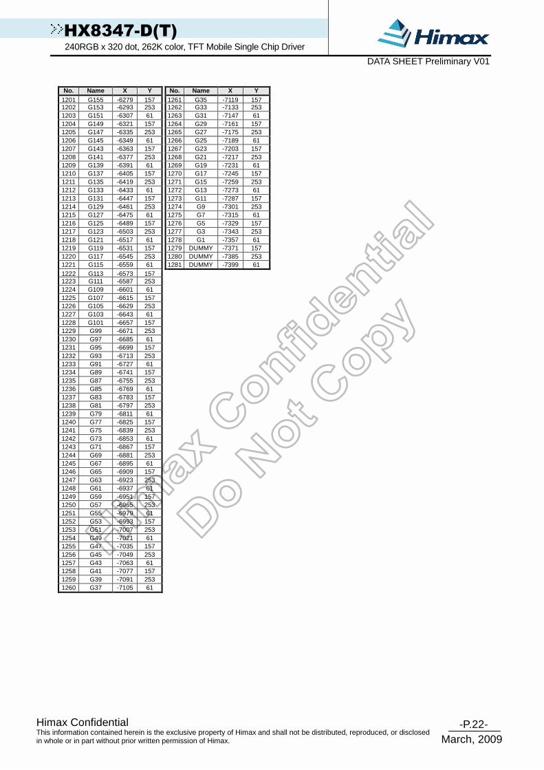
-P.22- Himax Confidential
March, 2009
This information contained herein is the exclusive property of Himax and shall not be distributed, reproduced, or disclosed in whole or in part without prior written permission of Himax.
HX8347-D(T) 240RGB x 320 dot, 262K color, TFT Mobile Single Chip Driver DATA SHEET Preliminary V01
No. Name X Y No. Name X Y
1201 G155 -6279 157 1261 G35 -7119 157 1202 G153 -6293 253 1262 G33 -7133 253 1203 G151 -6307 61 1263 G31 -7147 61 1204 G149 -6321 157 1264 G29 -7161 157 1205 G147 -6335 253 1265 G27 -7175 253 1206 G145 -6349 61 1266 G25 -7189 61 1207 G143 -6363 157 1267 G23 -7203 157 1208 G141 -6377 253 1268 G21 -7217 253 1209 G139 -6391 61 1269 G19 -7231 61 1210 G137 -6405 157 1270 G17 -7245 157 1211 G135 -6419 253 1271 G15 -7259 253 1212 G133 -6433 61 1272 G13 -7273 61 1213 G131 -6447 157 1273 G11 -7287 157 1214 G129 -6461 253 1274 G9 -7301 253 1215 G127 -6475 61 1275 G7 -7315 61 1216 G125 -6489 157 1276 G5 -7329 157 1217 G123 -6503 253 1277 G3 -7343 253 1218 G121 -6517 61 1278 G1 -7357 61 1219 G119 -6531 157 1279 DUMMY -7371 157 1220 G117 -6545 253 1280 DUMMY -7385 253 1221 G115 -6559 61 1281 DUMMY -7399 61 1222 G113 -6573 157 1223 G111 -6587 253 1224 G109 -6601 61 1225 G107 -6615 157 1226 G105 -6629 253 1227 G103 -6643 61 1228 G101 -6657 157 1229 G99 -6671 253 1230 G97 -6685 61 1231 G95 -6699 157 1232 G93 -6713 253 1233 G91 -6727 61 1234 G89 -6741 157 1235 G87 -6755 253 1236 G85 -6769 61 1237 G83 -6783 157 1238 G81 -6797 253 1239 G79 -6811 61 1240 G77 -6825 157 1241 G75 -6839 253 1242 G73 -6853 61 1243 G71 -6867 157 1244 G69 -6881 253 1245 G67 -6895 61 1246 G65 -6909 157 1247 G63 -6923 253 1248 G61 -6937 61 1249 G59 -6951 157 1250 G57 -6965 253 1251 G55 -6979 61 1252 G53 -6993 157 1253 G51 -7007 253 1254 G49 -7021 61 1255 G47 -7035 157 1256 G45 -7049 253 1257 G43 -7063 61 1258 G41 -7077 157 1259 G39 -7091 253
1260 G37 -7105 61

-P.23- Himax Confidential
March, 2009
This information contained herein is the exclusive property of Himax and shall not be distributed, reproduced, or disclosed in whole or in part without prior written permission of Himax.
HX8347-D(T) 240RGB x 320 dot, 262K color, TFT Mobile Single Chip Driver DATA SHEET Preliminary V01
4.4 Alignment mark
A_MARK (A1) A_MARK (A2)
B_MARK (B1) B_MARK (B2)

-P.24- Himax Confidential
March, 2009
This information contained herein is the exclusive property of Himax and shall not be distributed, reproduced, or disclosed in whole or in part without prior written permission of Himax.
HX8347-D(T) 240RGB x 320 dot, 262K color, TFT Mobile Single Chip Driver DATA SHEET Preliminary V01
4.5 Bump size
Input PAD
Output PAD
18X80 32um
18um 16um14um
80um
-P.25- Himax Confidential
March, 2009
This information contained herein is the exclusive property of Himax and shall not be distributed, reproduced, or disclosed in whole or in part without prior written permission of Himax.
HX8347-D(T) 240RGB x 320 dot, 262K color, TFT Mobile Single Chip Driver DATA SHEET Preliminary V01
5. Interface
The HX8347-D supports two-type interface group: Command-Parameter interface group, Register-Content interface group. This manual description focuses on Register-Content interface group. About the Command-Parameter interface mode, please refer to the HX8347-D (N) datasheet for detail. In Register-Content interface group (IFSEL = ‘L’), the HX8347-D has a system interface circuit for register command/GRAM data transferring, and a RGB interface circuit for display data transferring during animated display. The system interface circuit uses data bus pins (DB17-0). Since the data bus pins (DB17-0) can be used as input in RGB interface circuit, the HX8347-D shows animated display with less wiring. System interface can be used to access internal command and internal 18-bit/pixel GRAM. The RGB interface is only used to access display data. Please make sure that in RGB interface mode, the input display data is not written to GRAM and is displayed directly.
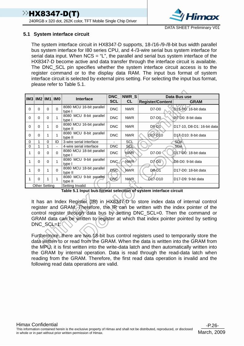
-P.26- Himax Confidential
March, 2009
This information contained herein is the exclusive property of Himax and shall not be distributed, reproduced, or disclosed in whole or in part without prior written permission of Himax.
HX8347-D(T) 240RGB x 320 dot, 262K color, TFT Mobile Single Chip Driver DATA SHEET Preliminary V01
5.1 System interface circuit The system interface circuit in HX8347-D supports, 18-/16-/9-/8-bit bus width parallel bus system interface for I80 series CPU, and 4-/3-wire serial bus system interface for serial data input. When NCS = “L”, the parallel and serial bus system interface of the HX8347-D become active and data transfer through the interface circuit is available. The DNC_SCL pin specifies whether the system interface circuit access is to the register command or to the display data RAM. The input bus format of system interface circuit is selected by external pins setting. For selecting the input bus format, please refer to Table 5.1.
Data Bus use IM3 IM2 IM1 IM0 Interface DNC_SCL
NWR_SCL Register/Content GRAM
0 0 0 0 8080 MCU 16-bit parallel type I
DNC NWR D7-D0 D15-D0: 16-bit data
0 0 0 1 8080 MCU 8-bit parallel type I
DNC NWR D7-D0 D7-D0: 8-bit data
0 0 1 0 8080 MCU 16-bit parallel type II DNC NWR D8-D1 D17-10, D8-D1: 16-bit data
0 0 1 1 8080 MCU 8-bit parallel type II DNC NWR D17-D10 D17-D10: 8-bit data
0 1 0 ID 3-wire serial interface - SCL SDA 0 1 1 - 4-wire serial interface DNC SCL SDA
1 0 0 0 8080 MCU 18-bit parallel type I DNC NWR D7-D0 D17-D0: 18-bit data
1 0 0 1 8080 MCU 9-bit parallel type I DNC NWR D7-D0 D8-D0: 9-bit data
1 0 1 0 8080 MCU 18-bit parallel type II
DNC NWR D8-D1 D17-D0: 18-bit data
1 0 1 1 8080 MCU 9-bit parallel type II DNC NWR D17-D10 D17-D9: 9-bit data
Other Setting Setting Invalid Table 5.1 Input bus format selection of system inte rface circuit
It has an Index Register (IR) in HX8347-D to store index data of internal control register and GRAM. Therefore, the IR can be written with the index pointer of the control register through data bus by setting DNC_SCL=0. Then the command or GRAM data can be written to register at which that index pointer pointed by setting DNC_SCL=1. Furthermore, there are two 18-bit bus control registers used to temporarily store the data written to or read from the GRAM. When the data is written into the GRAM from the MPU, it is first written into the write-data latch and then automatically written into the GRAM by internal operation. Data is read through the read-data latch when reading from the GRAM. Therefore, the first read data operation is invalid and the following read data operations are valid.

-P.27- Himax Confidential
March, 2009
This information contained herein is the exclusive property of Himax and shall not be distributed, reproduced, or disclosed in whole or in part without prior written permission of Himax.
HX8347-D(T) 240RGB x 320 dot, 262K color, TFT Mobile Single Chip Driver DATA SHEET Preliminary V01
5.1.1 Parallel bus system interface
The input / output data from data pins (DB17-0) and signal operation of the I80 series parallel bus interface are listed in Table 5.2.
Operations NWR_SCL NRD DNC_SCL
Writes Indexes into IR 0 1 0 Reads internal status 1 0 0 Writes command into register or data into GRAM 0 1 1 Reads command from register or data from GRAM 1 0 1
Table 5.2 Data pin function for I80 series CPU
Write to the register
Read the register
NCS
DNC_SCL
NWR_RNW
DB7-0 Command write to the register"index" write to index register
NCS
DNC_SCL
NRD_E
DB7-0 Command read from the register"index" write to index register
NWR_RNW
NRD_E
Figure 5.1 Register read/write timing in parallel b us system interface (for I80 series MPU)

-P.28- Himax Confidential
March, 2009
This information contained herein is the exclusive property of Himax and shall not be distributed, reproduced, or disclosed in whole or in part without prior written permission of Himax.
HX8347-D(T) 240RGB x 320 dot, 262K color, TFT Mobile Single Chip Driver DATA SHEET Preliminary V01
Write to the graphic RAM Write to the graphic RAM Write to the graphic RAM Write to the graphic RAM
DNC
NCS
"22" h 1st write data 3rd write data 4th write data2nd write data
Read the graphic RAM Read the graphic RAM Read the graphic RAM Read the graphic RAM
NRD_E
NWR_RNW
DNC
NCS
Dummy Read Data
"22" h
1st read data 2nd read read 3rd read data
NRD_E
NWR_RNW
DB[B:0]
DB[B:0]
5th write data
Figure 5.2 GRAM read/write timing in parallel bus s ystem interface (for I80 series MPU)

-P.29- Himax Confidential
March, 2009
This information contained herein is the exclusive property of Himax and shall not be distributed, reproduced, or disclosed in whole or in part without prior written permission of Himax.
HX8347-D(T) 240RGB x 320 dot, 262K color, TFT Mobile Single Chip Driver DATA SHEET Preliminary V01
5.1.2 MCU data color coding
MCU Data Color Coding for RAM data Write
- Parallel 8-Bit Bus Interface typeI (IM3,IM2,IM1,IM0=”0001”) DB17 DB16 DB15 DB14 DB13 DB12 DB11 DB10 DB9 DB8 DB7 DB6 DB5 DB4 DB3 DB2 DB1 DB0 Command Register
Command x x x x x x x x x x 0 0 1 0 0 0 1 0 22H 17H DB17 DB16 DB15 DB14 DB13 DB12 DB11 DB10 DB9 DB8 DB7 DB6 DB5 DB4 DB3 DB2 DB1 DB0 Color
x x x x x x x x x x R3 R2 R1 R0 G3 G2 G1 G0 x x x x x x x x x x B3 B2 B1 B0 R3 R2 R1 R0 03h x x x x x x x x x x G3 G2 G1 G0 B3 B2 B1 B0
4K-Color (2-pixels/ 3-bytes)
x x x x x x x x x x R4 R3 R2 R1 R0 G5 G4 G3 05h
x x x x x x x x x x G2 G1 G0 B4 B3 B2 B1 B0 65K-Color
(1-pixel/ 2-bytes)
x x x x x x x x x x R5 R4 R3 R2 R1 R0 x x x x x x x x x x x x G5 G4 G3 G2 G1 G0 x x 06h
x x x x x x x x x x B5 B4 B3 B2 B1 B0 x x
262K-Color (1-pixel/ 3bytes)
Table 5.3 8-bit parallel interface type I GRAM writ e table
- Parallel 16-Bit Bus Interface typeI (IM3,IM2,IM1,IM0=”0000”)
DB17 DB16 DB15 DB14 DB13 DB12 DB11 DB10 DB9 DB8 DB7 DB6 DB5 DB4 DB3 DB2 DB1 DB0 Command Register Command x x x x x x x x x x 0 0 1 0 0 0 1 0 22H
17H DB17 DB16 DB15 DB14 DB13 DB12 DB11 DB10 DB9 DB8 DB7 DB6 DB5 DB4 DB3 DB2 DB1 DB0 Color 03h R3 R2 R1 R0 G3 G2 G1 G0 B3 B2 B1 B0 4K-Color 05h x x R4 R3 R2 R1 R0 G5 G4 G3 G2 G1 G0 B5 B4 B3 B2 B1 65K-Color
x x R5 R4 R3 R2 R1 R0 x x G5 G4 G3 G2 G1 G0 x x x x B5 B4 B3 B2 B1 B0 x x R5 R4 R3 R2 R1 R0 x x 06h
x x G5 G4 G3 G2 G1 G0 x x B5 B4 B3 B2 B1 B0 x x
262K-Color (2-pixels/ 3bytes)
x x R5 R4 R3 R2 R1 R0 G5 G4 G3 G2 G1 G0 B5 B4 B3 B2 07h x x x x x x x x x x x x x x X x B1 B0
262K-Color (16+2)
Table 5.4 16-bit parallel interface type I GRAM wri te table
- Parallel 9-Bit Bus Interface typeI (IM3,IM2,IM1,IM0=”1001”) DB17 DB16 DB15 DB14 DB13 DB12 DB11 DB10 DB9 DB8 DB7 DB6 DB5 DB4 DB3 DB2 DB1 DB0 Register Register
Command x x x x x x x x x x 0 0 1 0 0 0 1 0 22H 17H DB17 DB16 DB15 DB14 DB13 DB12 DB11 DB10 DB9 DB8 DB7 DB6 DB5 DB4 DB3 DB2 DB1 DB0 Color
x x x x x x x x x R5 R4 R3 R2 R1 R0 G5 G4 G3 06h
x x x x x x x x x G2 G1 G0 B5 B4 B3 B2 B1 B0 262K-Color
(1-pixels/ 2bytes)
Table 5.5 9-bit parallel interface type I GRAM writ e table
- Parallel 18-Bit Bus Interface typeI (IM3,IM2,IM1,IM0=”1000”) DB17 DB16 DB15 DB14 DB13 DB12 DB11 DB10 DB9 DB8 DB7 DB6 DB5 DB4 DB3 DB2 DB1 DB0 Register Register
Command x x x x x x x x x x 0 0 1 0 0 0 1 0 22H 17H DB17 DB16 DB15 DB14 DB13 DB12 DB11 DB10 DB9 DB8 DB7 DB6 DB5 DB4 DB3 DB2 DB1 DB0 Color 06h R5 R4 R3 R2 R1 R0 G5 G4 G3 G2 G1 G0 B5 B4 B3 B2 B1 B0 262K-Color
Table 5.6 18-bit parallel interface type I GRAM wri te table

-P.30- Himax Confidential
March, 2009
This information contained herein is the exclusive property of Himax and shall not be distributed, reproduced, or disclosed in whole or in part without prior written permission of Himax.
HX8347-D(T) 240RGB x 320 dot, 262K color, TFT Mobile Single Chip Driver DATA SHEET Preliminary V01
- Parallel 8-Bit Bus Interface typeII (IM3,IM2,IM1,IM0=”0011”) DB17 DB16 DB15 DB14 DB13 DB12 DB11 DB10 DB9 DB8 DB7 DB6 DB5 DB4 DB3 DB2 DB1 DB0 Command Register
Command 0 0 1 0 0 0 1 0 x x x x x x x x x x 22H 17H DB17 DB16 DB15 DB14 DB13 DB12 DB11 DB10 DB9 DB8 DB7 DB6 DB5 DB4 DB3 DB2 DB1 DB0 Color
R3 R2 R1 R0 G3 G2 G1 G0 x x x x x x x x x x B3 B2 B1 B0 R3 R2 R1 R0 x x x x x x x x x x 03h
G3 G2 G1 G0 B3 B2 B1 B0 x x x x x x x x x x
4K-Color (2-pixels/ 3-bytes)
R4 R3 R2 R1 R0 G5 G4 G3 x x x x x x x x x x 05h
G2 G1 G0 B4 B3 B2 B1 B0 x x x x x x x x x x 65K-Color
(1-pixel/ 2-bytes)
R5 R4 R3 R2 R1 R0 x x x x x x x x x x x x G5 G4 G3 G2 G1 G0 x x x x x x x x x x x x 06h
B5 B4 B3 B2 B1 B0 x x x x x x x x x x x x
262K-Color (1-pixel/ 3bytes)
Table 5.7 8-bit parallel interface type II GRAM wri te table
- Parallel 16-Bit Bus Interface typeII (IM3,IM2,IM1,IM0=”0010”)
DB17 DB16 DB15 DB14 DB13 DB12 DB11 DB10 DB9 DB8 DB7 DB6 DB5 DB4 DB3 DB2 DB1 DB0 Command Register Command x 0 0 1 0 0 0 1 0 x 22H
17H DB17 DB16 DB15 DB14 DB13 DB12 DB11 DB10 DB9 DB8 DB7 DB6 DB5 DB4 DB3 DB2 DB1 DB0 Color 03h X x x x R3 R2 R1 R0 x G3 G2 G1 G0 B3 B2 B1 B0 x 4K-Color 05h R4 R3 R2 R1 R0 G5 G4 G3 x G2 G1 G0 B4 B3 B2 B1 B0 x 65K-Color
R5 R4 R3 R2 R1 R0 x x x G5 G4 G3 G2 G1 G0 x x x B5 B4 B3 B2 B1 B0 x x x R5 R4 R3 R2 R1 R0 x x x 06h
G5 G4 G3 G2 G1 G0 x x x B5 B4 B3 B2 B1 B0 x x x
262K-Color (2-pixels/ 3bytes)
R5 R4 R3 R2 R1 R0 G5 G4 x G3 G2 G1 G0 B5 B4 B3 B2 x 07h
B1 B0 x x x x x x x x x x x x x x 262K-Color (16+2)
Table 5.8 16-bit parallel interface type II GRAM wr ite set table
- Parallel 9-Bit Bus Interface typeII (IM3,IM2,IM1,IM0=”1011”)
D17 D16 D15 D14 D13 D12 D11 D10 D9 D8 D7 D6 D5 D4 D3 D2 D1 D0 Register Register Command 0 0 1 0 0 0 1 0 x x x x x x x x x x 22H
17H D8 D7 D6 D5 D4 D3 D2 D1 D0 D8 D7 D6 D5 D4 D3 D2 D1 D0 Color R5 R4 R3 R2 R1 R0 G5 G4 G3 x x x x x x x x x
06h G2 G1 G0 B5 B4 B3 B2 B1 B0 x x x x x x x x x
262K-Color (1-pixel/ 2bytes)
Table 5.9 9-bit parallel interface set type II GRAM write table
- Parallel 18-Bit Bus Interface typeII (IM3,IM2,IM1,IM0=”1010”) DB17 DB16 DB15 DB14 DB13 DB12 DB11 DB10 DB9 DB8 DB7 DB6 DB5 DB4 DB3 DB2 DB1 DB0 Register Register
Command X x x x x x x x x 0 0 1 0 0 0 1 0 x 22H 17H DB17 DB16 DB15 DB14 DB13 DB12 DB11 DB10 DB9 DB8 DB7 DB6 DB5 DB4 DB3 DB2 DB1 DB0 Color 06h R5 R4 R3 R2 R1 R0 G5 G4 G3 G2 G1 G0 B5 B4 B3 B2 B1 B0 262K-Color
Table 5.10 18-bit parallel interface type II GRAM w rite set table

-P.31- Himax Confidential
March, 2009
This information contained herein is the exclusive property of Himax and shall not be distributed, reproduced, or disclosed in whole or in part without prior written permission of Himax.
HX8347-D(T) 240RGB x 320 dot, 262K color, TFT Mobile Single Chip Driver DATA SHEET Preliminary V01
18-bit parallel bus system interface The I80-system 18-bit parallel bus interface type I in command-parameter interface mode can be used by setting external pins “IM3, IM2, IM1, IM0” pins to “1000”. And the I80-system 18-bit parallel bus interface type II in command-parameter interface mode can be used by setting ““IM3, IM2, IM1, IM0” pins to “1010”. Figure 5.3 is the example of interface with I80 microcomputer system interface.
/HXHXHXHX8347834783478347----DDDD
18
MPUMPUMPUMPU NWR_SCL
NRD
NCS
DB17-0
DNC_SCL
Figure 5.3 Example of I80- system 18-bit parallel b us interface
Figure 5.4 Input data bus and GRAM data mapping in 18-bit bus system interface with 18-bit-data Input
(“IM3, IM2, IM1, IM”=”1010” or “1000”)

-P.32- Himax Confidential
March, 2009
This information contained herein is the exclusive property of Himax and shall not be distributed, reproduced, or disclosed in whole or in part without prior written permission of Himax.
HX8347-D(T) 240RGB x 320 dot, 262K color, TFT Mobile Single Chip Driver DATA SHEET Preliminary V01
16-bit parallel bus system interface The I80-system 16-bit parallel bus interface type I in command-parameter interface mode can be used by setting external pins ““IM3, IM2, IM1, IM0” pins to “0000”. And I80-system 16-bit parallel bus interface type II in command-parameter interface mode can be used by setting ““IM3, IM2, IM1, IM0” pins to “0010”. Figure 5.5 is the example of type I interface with I80 microcomputer system interface. And Figure 5.6 is the example of type II interface with I80 microcomputer system interface.
Figure 5.5 Example of I80 system 16-bit parallel bu s interface type I
Figure 5.6 Example of I80 system 16-bit parallel bu s interface type II

-P.33- Himax Confidential
March, 2009
This information contained herein is the exclusive property of Himax and shall not be distributed, reproduced, or disclosed in whole or in part without prior written permission of Himax.
HX8347-D(T) 240RGB x 320 dot, 262K color, TFT Mobile Single Chip Driver DATA SHEET Preliminary V01
Figure 5.7 Input data bus and GRAM data mapping in 16-bit bus system interface with 12-bit-data input
(R17H=03h and “IM3, IM2, IM1, IM0”=”0000”)
Figure 5.8 Input data bus and GRAM data mapping in 16-bit bus system interface with 16-bit-data input
(R17H=05h and “IM3, IM2, IM1, IM0”=”0000”)
GRAM Data
Input Data
Bus
Transfer
Order16- bit Data
1
B5 B4 B3 B2 B1 B0
262, 144 colors are available
DB
15
DB
14
DB
13
DB
12
DB
11
DB
10
DB
7
DB
6
DB
5
DB
4
DB
3
DB
2
R5 R4 R3 R2 R1 R0 G5 G4 G3 G2 G1 G0
16- bit Data
2
DB
15
DB
14
DB
13
DB
12
DB
11
DB
10
DB
7
DB
6
DB
5
DB
4
DB
3
DB
2
R5 R4 R3 R2 R1 R0
1st pixel
Figure 5.9 Input data bus and GRAM data mapping in 16-bit bus system interface with 18 bit-data input
(R17H=06h and “IM3, IM2, IM1, IM0”=”0000”)
Figure 5.10 Input data bus and GRAM data mapping in 16-bit bus system interface with 18(16+2) bit-data input ( R17H=07h and “IM3, IM2, IM1, IM0”=”0000”)
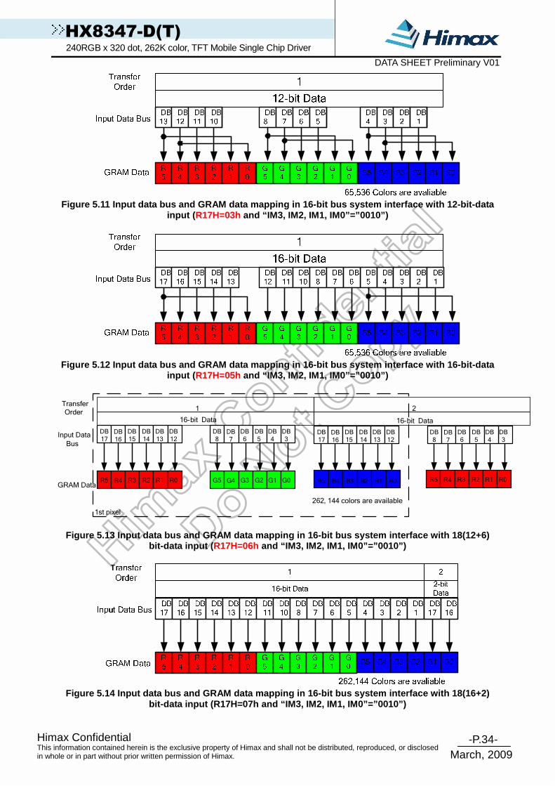
-P.34- Himax Confidential
March, 2009
This information contained herein is the exclusive property of Himax and shall not be distributed, reproduced, or disclosed in whole or in part without prior written permission of Himax.
HX8347-D(T) 240RGB x 320 dot, 262K color, TFT Mobile Single Chip Driver DATA SHEET Preliminary V01
Figure 5.11 Input data bus and GRAM data mapping in 16-bit bus system interface with 12-bit-data
input ( R17H=03h and “IM3, IM2, IM1, IM0”=”0010”)
Figure 5.12 Input data bus and GRAM data mapping in 16-bit bus system interface with 16-bit-data
input ( R17H=05h and “IM3, IM2, IM1, IM0”=”0010”)
GRAM Data
Input Data
Bus
TransferOrder
16-bit Data
1
B5 B4 B3 B2 B1 B0
262, 144 colors are available
DB17
DB16
DB15
DB14
DB13
DB12
DB8
DB7
DB6
DB5
DB4
DB3
R5 R4 R3 R2 R1 R0 G5 G4 G3 G2 G1 G0
16-bit Data
2
R5 R4 R3 R2 R1 R0
1st pixel
DB17
DB16
DB15
DB14
DB13
DB12
DB8
DB7
DB6
DB5
DB4
DB3
Figure 5.13 Input data bus and GRAM data mapping in 16-bit bus system interface with 18(12+6)
bit-data input ( R17H=06h and “IM3, IM2, IM1, IM0”=”0010”)
Figure 5.14 Input data bus and GRAM data mapping in 16-bit bus system interface with 18(16+2)
bit-data input (R17H=07h and “IM3, IM2, IM1, IM0”=” 0010”)
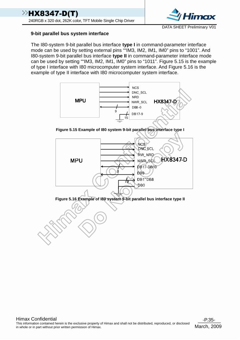
-P.35- Himax Confidential
March, 2009
This information contained herein is the exclusive property of Himax and shall not be distributed, reproduced, or disclosed in whole or in part without prior written permission of Himax.
HX8347-D(T) 240RGB x 320 dot, 262K color, TFT Mobile Single Chip Driver DATA SHEET Preliminary V01
9-bit parallel bus system interface The I80-system 9-bit parallel bus interface type I in command-parameter interface mode can be used by setting external pins ““IM3, IM2, IM1, IM0” pins to “1001”. And I80-system 9-bit parallel bus interface type II in command-parameter interface mode can be used by setting ““IM3, IM2, IM1, IM0” pins to “1011”. Figure 5.15 is the example of type I interface with I80 microcomputer system interface. And Figure 5.16 is the example of type II interface with I80 microcomputer system interface.
/HXHXHXHX8347834783478347----DDDD
9DB17-9/
15
MPUMPUMPUMPU NWR_SCL
NRD
NCS
DB8 -0
DNC_SCL
Figure 5.15 Example of I80 system 9-bit parallel bu s interface type I
Figure 5.16 Example of I80 system 9-bit parallel bu s interface type II

-P.36- Himax Confidential
March, 2009
This information contained herein is the exclusive property of Himax and shall not be distributed, reproduced, or disclosed in whole or in part without prior written permission of Himax.
HX8347-D(T) 240RGB x 320 dot, 262K color, TFT Mobile Single Chip Driver DATA SHEET Preliminary V01
GRAM Data
Input Data Bus
Transfer Order
9-bit Data
262,144 Colors are available
R5 R4 R3 R2 R1 R0 G5 G4 G3 G2 G1 G0 B5 B4 B3 B2 B1 B0
DB8
DB7
DB6
DB5
DB4
DB3
DB2
DB1
DB8
DB7
DB6
DB5
DB4
DB3
DB2
DB1
1 2
9-bit Data
DB0
DB0
Figure 5.17 Input data bus and GRAM data mapping in 9-bit bus system interface with 18-bit-data input (R17H=06h and “IM3, IM2, IM1, IM0”=”1001”)
GRAM Data
Input Data Bus
Transfer Order
9-bit Data
262,144 Colors are available
R5 R4 R3 R2 R1 R0 G5 G4 G3 G2 G1 G0 B5 B4 B3 B2 B1 B0
DB17
DB16
DB15
DB14
DB13
DB12
DB11
DB10
DB17
DB16
DB15
DB14
DB13
DB12
DB11
DB10
1 2
9-bit Data
DB9
DB9
Figure 5.18 Input data bus and GRAM data mapping in 9-bit bus system interface with 18-bit-data input (R17H=06h and “IM3, IM2, IM1, IM0”=”1011”)
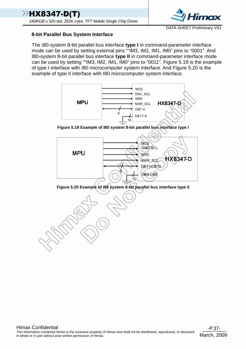
-P.37- Himax Confidential
March, 2009
This information contained herein is the exclusive property of Himax and shall not be distributed, reproduced, or disclosed in whole or in part without prior written permission of Himax.
HX8347-D(T) 240RGB x 320 dot, 262K color, TFT Mobile Single Chip Driver DATA SHEET Preliminary V01
8-bit Parallel Bus System Interface The I80-system 8-bit parallel bus interface type I in command-parameter interface mode can be used by setting external pins ““IM3, IM2, IM1, IM0” pins to “0001”. And I80-system 8-bit parallel bus interface type II in command-parameter interface mode can be used by setting ““IM3, IM2, IM1, IM0” pins to “0011”. Figure 5.19 is the example of type I interface with I80 microcomputer system interface. And Figure 5.20 is the example of type II interface with I80 microcomputer system interface.
/HXHXHXHX8347834783478347----DDDD
8DB17- 8/
16
MPUMPUMPUMPU NWR_SCL
NRD
NCS
DB7 -0
DNC_SCL
Figure 5.19 Example of I80 system 8-bit parallel bu s interface type I
Figure 5.20 Example of I80 system 8-bit parallel bu s interface type II

-P.38- Himax Confidential
March, 2009
This information contained herein is the exclusive property of Himax and shall not be distributed, reproduced, or disclosed in whole or in part without prior written permission of Himax.
HX8347-D(T) 240RGB x 320 dot, 262K color, TFT Mobile Single Chip Driver DATA SHEET Preliminary V01
GRAM Data
Input Bata Bus
Transfer Order
8-bit Data
4,096 Colors are available
R5 R4 R3 R2 R1 R0 G5 G4 G3 G2 G1 G0 B5 B4 B3 B2 B1 B0
DB7
DB6
DB5
DB4
DB3
DB2
DB1
DB0
DB7
DB6
DB5
DB4
1 2
4-bit Data
Figure 5.21 Input data bus and GRAM data mapping in 8-bit bus system interface with 12-bit-data input (R17H=03h and“IM3, IM2, IM1, IM0”=”0001”)
GRAM Data
Input Data Bus
Transfer Order
8-bit Data
65,536 Colors are available
R5 R4 R3 R2 R1 R0 G5 G4 G3 G2 G1 G0 B5 B4 B3 B2 B1 B0
DB7
DB6
DB5
DB4
DB3
DB2
DB1
DB0
DB7
DB6
DB5
DB4
DB3
DB2
DB1
DB0
1 2
8-bit Data
Figure 5.22 Input data bus and GRAM data mapping in 8-bit bus system interface with 16-bit-data input (R17H=05h and “IM3, IM2, IM1, IM0”=”0001”)
GRAM Data
Transfer Order
6-bit Data
262,144 Colors are available
R5 R4 R3 R2 R1 R0 G5 G4 G3 G2 G1 G0 B5 B4 B3 B2 B1 B0
DB7
DB6
DB5
DB4
DB3
DB7
DB6
DB5
DB4
DB3
DB2
DB7
DB6
DB5
DB4
DB3
1
DB2
DB2
3
6-bit Data6-bit Data
2
Figure 5.23 Input data bus and GRAM data mapping in 8-bit bus system interface with 18-bit-data input (R17H=06h and “IM3, IM2, IM1, IM0”=”0001”)

-P.39- Himax Confidential
March, 2009
This information contained herein is the exclusive property of Himax and shall not be distributed, reproduced, or disclosed in whole or in part without prior written permission of Himax.
HX8347-D(T) 240RGB x 320 dot, 262K color, TFT Mobile Single Chip Driver DATA SHEET Preliminary V01
GRAM Data
Input Bata Bus
Transfer Order
8-bit Data
4,096 Colors are available
R5 R4 R3 R2 R1 R0 G5 G4 G3 G2 G1 G0 B5 B4 B3 B2 B1 B0
DB17
DB16
DB15
DB14
DB13
DB12
DB11
DB10
DB17
DB16
DB15
DB14
1 2
4-bit Data
Figure 5.24 Input data bus and GRAM data mapping in 8-bit bus system interface with 12-bit-data input (R17H=03h and“IM3, IM2, IM1, IM0”=”0011”)
GRAM Data
Input Data Bus
Transfer Order
8-bit Data
65,536 Colors are available
R5 R4 R3 R2 R1 R0 G5 G4 G3 G2 G1 G0 B5 B4 B3 B2 B1 B0
DB17
DB16
DB15
DB14
DB13
DB12
DB11
DB10
DB17
DB16
DB15
DB14
DB13
DB12
DB11
DB10
1 2
8-bit Data
Figure 5.25 Input data bus and GRAM data mapping in 8-bit bus system interface with 16-bit-data input
(R17H=05h and “IM3, IM2, IM1, IM0”=”0011”)
GRAM Data
Transfer Order
6-bit Data
262,144 Colors are available
R5 R4 R3 R2 R1 R0 G5 G4 G3 G2 G1 G0 B5 B4 B3 B2 B1 B0
DB17
DB16
DB15
DB14
DB13
DB17
DB16
DB15
DB14
DB13
DB12
DB17
DB16
DB15
DB14
DB13
1
DB12
DB12
3
6-bit Data6-bit Data
2
Figure 5.26 Input data bus and GRAM data mapping in 8-bit bus system interface with 18-bit-data input (R17H=06h and “IM3, IM2, IM1, IM0”=”0011”)

-P.40- Himax Confidential
March, 2009
This information contained herein is the exclusive property of Himax and shall not be distributed, reproduced, or disclosed in whole or in part without prior written permission of Himax.
HX8347-D(T) 240RGB x 320 dot, 262K color, TFT Mobile Single Chip Driver DATA SHEET Preliminary V01
MCU Data Color Coding for RAM data Read
- Parallel 8-Bit Bus Interface type I (IM3,IM2,IM1,IM0=”0001”) D17 D16 D15 D14 D13 D12 D11 D10 D9 D8 D7 D6 D5 D4 D3 D2 D1 D0 Command Register
Command x x x x x x x x x x 0 0 1 0 0 0 1 0 22H D17 D16 D15 D14 D13 D12 D11 D10 D9 D8 D7 D6 D5 D4 D3 D2 D1 D0 Color x x x x x x x x x x x x x x x x x x Dummy Read x x x x x x x x x x R5 R4 R3 R2 R1 R0 x x x x x x x x x x x x G5 G4 G3 G2 G1 G0 x x
Read Data Format
x x x x x x x x x x B5 B4 B3 B2 B1 B0 x x
262K-Color (1-pixel/ 3bytes)
Table 5.11 8-bit parallel interface type I GRAM rea d table
- Parallel 16-Bit Bus Interface type I (IM3,IM2,IM1,IM0=”0000”) D17 D16 D15 D14 D13 D12 D11 D10 D9 D8 D7 D6 D5 D4 D3 D2 D1 D0 Command Register
Command x x x x x x x x x x 0 0 1 0 0 0 1 0 22H D17 D16 D15 D14 D13 D12 D11 D10 D9 D8 D7 D6 D5 D4 D3 D2 D1 D0 Color x x x x x x x x x x x x x x x x x x Dummy Read x x R5 R4 R3 R2 R1 R0 x x G5 G4 G3 G2 G1 G0 x x x x B5 B4 B3 B2 B1 B0 x x R5 R4 R3 R2 R1 R0 x x
Read Data Format
x x G5 G4 G3 G2 G1 G0 x x B5 B4 B3 B2 B1 B0 x x
262K-Color (2-pixels/ 3bytes)
Table 5.12 16-bit parallel interface type I GRAM re ad table
- Parallel 9-Bit Bus Interface type I (IM3,IM2,IM1,IM0=”1001”) D17 D16 D15 D14 D13 D12 D11 D10 D9 D8 D7 D6 D5 D4 D3 D2 D1 D0 Register Register
Command x x x x x x x x x x 0 0 1 0 0 0 1 0 22H D17 D16 D15 D14 D13 D12 D11 D10 D9 D8 D7 D6 D5 D4 D3 D2 D1 D0 Color x x x x x x x x x x x x x x x x x x Dummy Read x x x x x x x x x R5 R4 R3 R2 R1 R0 G5 G4 G3
Read Data Format
x x x x x x x x x G2 G1 G0 B5 B4 B3 B2 B1 B0 262K-Color
(1-pixel/ 2bytes)
Table 5.13 9-bit parallel interface type I GRAM rea d table
- Parallel 18-Bit Bus Interface type I (IM3,IM2,IM1,IM0=”1000”) D17 D16 D15 D14 D13 D12 D11 D10 D9 D8 D7 D6 D5 D4 D3 D2 D1 D0 Register Register
Command x x x x x x x x x x 0 0 1 0 0 0 1 0 22H D17 D16 D15 D14 D13 D12 D11 D10 D9 D8 D7 D6 D5 D4 D3 D2 D1 D0 Color x x x x x x x x x x x x x x x x x x Dummy Read
Read Data Format
R5 R4 R3 R2 R1 R0 G5 G4 G3 G2 G1 G0 B5 B4 B3 B2 B1 B0 262K-Color
Table 5.14 18-bit parallel interface type I GRAM re ad table

-P.41- Himax Confidential
March, 2009
This information contained herein is the exclusive property of Himax and shall not be distributed, reproduced, or disclosed in whole or in part without prior written permission of Himax.
HX8347-D(T) 240RGB x 320 dot, 262K color, TFT Mobile Single Chip Driver DATA SHEET Preliminary V01
- Parallel 8-Bit Bus Interface type II (IM3,IM2,IM1,IM0=”0011”) DB17 DB16 DB15 DB14 DB13 DB12 DB11 DB10 DB9 DB8 DB7 DB6 DB5 DB4 DB3 DB2 DB1 DB0 Command Register
Command 0 0 1 0 0 0 1 0 x x x x x x x x x x 22H DB17 DB16 DB15 DB14 DB13 DB12 DB11 DB10 DB9 DB8 DB7 DB6 DB5 DB4 DB3 DB2 DB1 DB0 Color
x x x x x x x x x x x x x x x x x x Dummy Read R5 R4 R3 R2 R1 R0 x x G5 G4 G3 G2 G1 G0 x x x x x x x x x x x x
Read Data Format
B5 B4 B3 B2 B1 B0 x x x x x x x x x x x x
262K-Color (1-pixel/ 3bytes)
Table 5.15 8-bit parallel interface type II GRAM re ad table
- Parallel 16-Bit Bus Interface type II (IM3,IM2,IM1,IM0=”0010”) DB17 DB16 DB15 DB14 DB13 DB12 DB11 DB10 DB9 DB8 DB7 DB6 DB5 DB4 DB3 DB2 DB1 DB0 Command Register
Command x x x x x x x x x 0 0 1 0 0 0 1 0 x 22H DB17 DB16 DB15 DB14 DB13 DB12 DB11 DB10 DB9 DB8 DB7 DB6 DB5 DB4 DB3 DB2 DB1 DB0 Color
x x x x x x x x x x x x x x x x Dummy Read R5 R4 R3 R2 R1 R0 x x x G5 G4 G3 G2 G1 G0 x x x B5 B4 B3 B2 B1 B0 x x x R5 R4 R3 R2 R1 R0 x x x
Read Data Format
G5 G4 G3 G2 G1 G0 x x x B5 B4 B3 B2 B1 B0 x x x
262K-Color (2-pixels/ 3bytes)
Table 5.16 16-bit parallel interface type II GRAM r ead table
- Parallel 9-Bit Bus Interface type II (IM3,IM2,IM1,IM0=”1011”) D17 D16 D15 D14 D13 D12 D11 D10 D9 D8 D7 D6 D5 D4 D3 D2 D1 D0 Register Register
Command 0 0 1 0 0 0 1 0 x x x x x x x x x X 22H D17 D16 D15 D14 D13 D12 D11 D10 D9 D8 D7 D6 D5 D4 D3 D2 D1 D0 Color x x x x x x x x x x x x x x x x x x Dummy Read
R5 R4 R3 R2 R1 R0 G5 G4 G3 x x x x x x x x x Read
Data Format
G2 G1 G0 B5 B4 B3 B2 B1 B0 x x x x x x x x x 262K-Color
(1-pixel/ 2bytes)
Table 5.17 9-bit parallel interface type II GRAM re ad table
- Parallel 18-Bit Bus Interface type II (IM3,IM2,IM1,IM0=”1010”) D17 D16 D15 D14 D13 D12 D11 D10 D9 D8 D7 D6 D5 D4 D3 D2 D1 D0 Register Register
Command x x x x x x x x x 0 0 1 0 0 0 1 0 x 22H D17 D16 D15 D14 D13 D12 D11 D10 D9 D8 D7 D6 D5 D4 D3 D2 D1 D0 Color x x x x x x x x x x x x x x x x x x Dummy Read
Read Data Format
R5 R4 R3 R2 R1 R0 G5 G4 G3 G2 G1 G0 B5 B4 B3 B2 B1 B0 262K-Color
Table 5.18 18-bit parallel interface type II GRAM r ead table
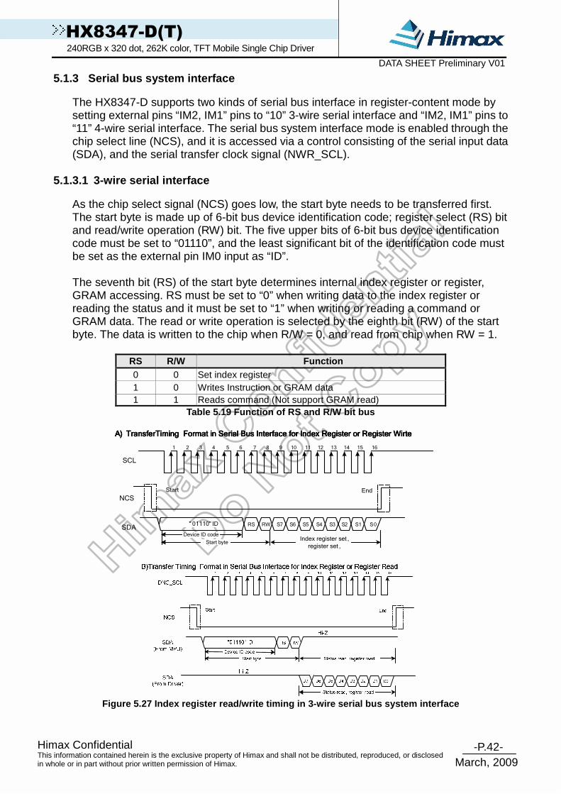
-P.42- Himax Confidential
March, 2009
This information contained herein is the exclusive property of Himax and shall not be distributed, reproduced, or disclosed in whole or in part without prior written permission of Himax.
HX8347-D(T) 240RGB x 320 dot, 262K color, TFT Mobile Single Chip Driver DATA SHEET Preliminary V01
5.1.3 Serial bus system interface The HX8347-D supports two kinds of serial bus interface in register-content mode by setting external pins “IM2, IM1” pins to “10” 3-wire serial interface and “IM2, IM1” pins to “11” 4-wire serial interface. The serial bus system interface mode is enabled through the chip select line (NCS), and it is accessed via a control consisting of the serial input data (SDA), and the serial transfer clock signal (NWR_SCL).
5.1.3.1 3-wire serial interface As the chip select signal (NCS) goes low, the start byte needs to be transferred first. The start byte is made up of 6-bit bus device identification code; register select (RS) bit and read/write operation (RW) bit. The five upper bits of 6-bit bus device identification code must be set to “01110”, and the least significant bit of the identification code must be set as the external pin IM0 input as “ID”. The seventh bit (RS) of the start byte determines internal index register or register, GRAM accessing. RS must be set to “0” when writing data to the index register or reading the status and it must be set to “1” when writing or reading a command or GRAM data. The read or write operation is selected by the eighth bit (RW) of the start byte. The data is written to the chip when R/W = 0, and read from chip when RW = 1.
RS R/W Function 0 0 Set index register 1 0 Writes Instruction or GRAM data 1 1 Reads command (Not support GRAM read)
Table 5.19 Function of RS and R/W bit bus
Device ID code
Start End
AAAA)))) TransferTiming Format in Serial Bus Interface for Index Register or Register Wirte TransferTiming Format in Serial Bus Interface for Index Register or Register Wirte TransferTiming Format in Serial Bus Interface for Index Register or Register Wirte TransferTiming Format in Serial Bus Interface for Index Register or Register Wirte
" 01110" ID
Start byteIndex register set ,
register set ,
1 2 3 4 5 6 7 8 9 10 11 12 13 14 15 16
RS RW S6 S5 S4 S3 S2 S1 S0S7
SCL
NCS
SDA
Figure 5.27 Index register read/write timing in 3-w ire serial bus system interface
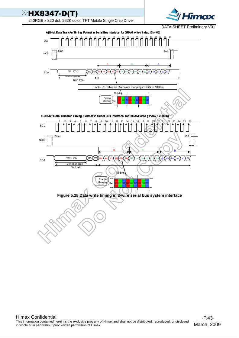
-P.43- Himax Confidential
March, 2009
This information contained herein is the exclusive property of Himax and shall not be distributed, reproduced, or disclosed in whole or in part without prior written permission of Himax.
HX8347-D(T) 240RGB x 320 dot, 262K color, TFT Mobile Single Chip Driver DATA SHEET Preliminary V01
Device ID code
Start End
AAAA) ) ) ) 16161616----bit Data Transfer Timing Format in Serial Bus Interface for GRAM write bit Data Transfer Timing Format in Serial Bus Interface for GRAM write bit Data Transfer Timing Format in Serial Bus Interface for GRAM write bit Data Transfer Timing Format in Serial Bus Interface for GRAM write ( ( ( ( Index Index Index Index 17171717hhhh= = = = 05050505))))
"01110" ID
Start byte
1 2 3 4 5 6 7 8 9 10 11 12 13 14 15 16 17 18 20 21 22 23 2419
RS RW
R G B
SCL
SDA
(1-0)= 00 ( 16 bit , 65k
-
R5 R4 R3 R2 R1 G5 G4 G3 G2 G1 G0 B5 B4 B3 B2 B1
Look - Up Table for 65k colors mapping (16Bits to 18Bits)
R1 G1 B1 R2 G2 B2 R3 G3 B3
Frame Memory
18-bits
NCS
Device ID code
Start End
NCS
BBBB) ) ) )
" 01110" ID
Start byte
1 2 3 4 5 6 7 8 9 10 11 12 13 14 15 16 17 18 20 21 22 23 2419
RS RW
2625
BGR
SCL
SDA
18181818----bit Data Transfer Timing Format in Serial Bus Interface for GRAM write bit Data Transfer Timing Format in Serial Bus Interface for GRAM write bit Data Transfer Timing Format in Serial Bus Interface for GRAM write bit Data Transfer Timing Format in Serial Bus Interface for GRAM write ( ( ( ( Index Index Index Index 17171717HHHH====06060606))))
16 bit , 65k
R3 R2 R1 R0 G5 G4 G3 G2 G1 G0 B5 B4 B3 B2 B1 B0R4R5
R1 G1 B1 R2 G2 B2 R3 G3 B3
18-bits
Frame Memory
Figure 5.28 Data write timing in 3-wire serial bus system interface

-P.44- Himax Confidential
March, 2009
This information contained herein is the exclusive property of Himax and shall not be distributed, reproduced, or disclosed in whole or in part without prior written permission of Himax.
HX8347-D(T) 240RGB x 320 dot, 262K color, TFT Mobile Single Chip Driver DATA SHEET Preliminary V01
5.1.3.2 4-wire serial interface 4-pin serial case, data packet contains just transmission byte and control bit DNC is transferred by DNC pin. If DNC is low, the transmission byte is command byte. If DNC is high, the transmission byte is stored to index register or GRAM. The MSB is transmitted first. The serial interface is initialized when NCS is high. In this state, NWR_SCL clock pulse or SDA data have no effect. A falling edge on NCS enables the serial interface and indicates the start of data transmission.
NCS
NWR_SCL
SDA
4444----Wire Serial Peripheral Interface ProtocolWire Serial Peripheral Interface ProtocolWire Serial Peripheral Interface ProtocolWire Serial Peripheral Interface Protocol
Command
NCS can be "H" betweenCommand and parameter
Parameter
D0D1D2D3D4D5D6D7D1 D0D2D3D4D5D6D7
DNC
Figure 5.29 Index register write timing in 4-wire s erial bus system interface
16-bit
Look-Up Table for 65K data mapping (16-bit to 18 bit)
R1 G1 B1 R2 G2 B2
18-bitGRAM
R12 R10R11 B10B11
SCL
SDA B12B13R13 G12 G10G11G13 B14G15 G14R14
16-bit Data Transfer Timing Format in 4-wire Seria l Bus Interface for GRAM write ( Index 17h= 05)
R1 G1 B1 R2 G2 B2 R3 G3 B3
GRAM
R12 R10R11 B10B11
SCL
SDA B12B13R13 G12 G10G11G13 B14G15 G14R14R15 B15
18-bit
18-bit Data Transfer Timing Format in 4-wire Serial Bus Interface for GRAM write ( Index 17h= 06)
Figure 5.30 Data write timing in 4-wire serial bus system interface

-P.45- Himax Confidential
March, 2009
This information contained herein is the exclusive property of Himax and shall not be distributed, reproduced, or disclosed in whole or in part without prior written permission of Himax.
HX8347-D(T) 240RGB x 320 dot, 262K color, TFT Mobile Single Chip Driver DATA SHEET Preliminary V01
5.2 RGB Interface The HX8347-D uses RCM [1:0] =’10’ or ‘11’ hardware setting to select RGB interface. After Power on Sequence, the RGB interface is activated. When RCM [1:0] =’10’ use VSYNC, HSYNC, DE, DOTCLK, DB17-0 parallel lines for the RGB interface (RGB mode 1). When RCM [1:0] =’11’ use VSYNC, HSYNC, DOTCLK, DB17-0 parallel lines for the RGB interface (RGB mode 2) Pixel clock (DOTCLK) must be running all the time without stopping and it is used to entering VSYNC, HSYNC, DE and DB17-0 lines states when there is a rising edge of the DOTCLK. In RGB interface mode 1, the valid display data is inputted in pixel unit via DB17-0 according to the high-level(‘H’) of DE signal, and display operations are executed in synchronization with the frame synchronizing signal (VSYNC), line synchronizing signal (HSYNC) and pixel clock (DOTCLK). In RGB interface mode 2, the valid display data is inputted in pixel unit via DB17-0 according to the HBP setting of HSYNC signal, and the VBP setting of VSYNC. In these two RGB interface modes, the input display data is not written to GRAM and is displayed directly. Vertical synchronization (VSYNC) signal is used to tell when there a new frame of the display is received , and this is negative (‘-‘, ‘0’, low) active. Horizontal synchronization signal (HSYNC) is used to tell when a new line of the frame is received, and this is negative (‘-‘, ‘0’, low) active. Data enable (DE) is used to tell when RGB information is received that should be transferred on the display, and this is positive (‘+’, ‘1’, high) active. DB17-0 are used to tell what the information of the image is, that is transferred on the display when DE=’H’. The pixel clock cycle is described in the following figure.
DOTCLK
VSYNC
HSYNCDE
DB17-0
Figure 5.31 DOTCLK cycle

-P.46- Himax Confidential
March, 2009
This information contained herein is the exclusive property of Himax and shall not be distributed, reproduced, or disclosed in whole or in part without prior written permission of Himax.
HX8347-D(T) 240RGB x 320 dot, 262K color, TFT Mobile Single Chip Driver DATA SHEET Preliminary V01
General timing diagram in RGB interface is as follow.
Invisible Image= Timing information what is not possible to see on the display
= Blanking Time
DE = ‘0’ (Low)
Visible Image= Image which can see on the display
= Active
DE = ‘1' (high)
10
VDISP
VFP
VBP
VP
1
0
HBP HDISP HFP
HP
Horizontal Sync.
Vertical Sync.
Figure 5.32 RGB interface circuit input timing diag ram The image information is correct on the display when the timings are in range on the interface. However, the image information will be incorrect on the display, when timings are out of the range on the RGB interface and the correct image information will be displayed automatically (by the display module) on the next frame (vertical sync.), when there is returned from out of the range to in range RGB interface timings.

-P.47- Himax Confidential
March, 2009
This information contained herein is the exclusive property of Himax and shall not be distributed, reproduced, or disclosed in whole or in part without prior written permission of Himax.
HX8347-D(T) 240RGB x 320 dot, 262K color, TFT Mobile Single Chip Driver DATA SHEET Preliminary V01
Note: (1) RGB mode 2 doesn’t need DE signal
(2) EPL=’0’, VSPL=’0’, HSPL=’0’ and DPL=’0’ of SETRGBIF (32H) command.
Figure 5.33 RGB mode timing diagram
VS
V Back Porch (TVBP)
V Front Porch (TVFP)
1-Frame (TVP)
1-Line (THP)
H Back Porch (THBP)
H Front Porch (THFP) Valid data area (THDISP)
D1 Dn D5 D3 D4 D2 In-Valid In-Valid
D1 D5 D3 D4 D2 In-Valid Dn
HS
DE
HS
DOTCLK
DE
Data Bus
Latch data

-P.48- Himax Confidential
March, 2009
This information contained herein is the exclusive property of Himax and shall not be distributed, reproduced, or disclosed in whole or in part without prior written permission of Himax.
HX8347-D(T) 240RGB x 320 dot, 262K color, TFT Mobile Single Chip Driver DATA SHEET Preliminary V01
All 3 kinds of bus width can be available during RGB interface mode (selected by COLMOD (17H) command for 6-bit, 16-bit and 18-bit data width)
17H D17 D16 D15 D14 D13 D12 D11 D10 D9 D8 D7 D6 D5 D4 D3 D2 D1 D0 Bus width 50h R4 R3 R2 R1 R0 x G5 G4 G3 G2 G1 G0 B4 B3 B2 B1 B0 x 16-bit data 60h R5 R4 R3 R2 R1 R0 G5 G4 G3 G2 G1 G0 B5 B4 B3 B2 B1 B0 18-bit data 17H D17 D16 D15 D14 D13 D12 D11 D10 D9 D8 D7 D6 D5 D4 D3 D2 D1 D0 Bus width
x x x x x x x x x x R5 R4 R3 R2 R1 R0 x x x x x x x x x x x x G5 G4 G3 G2 G1 G0 x x E0h x x x x x x x x x x B5 B4 B3 B2 B1 B0 x x
6-bit data
Note: (1) When 17H=”E0h”, 6-bit data width of 3-time transfer is used to transmit 1 pixel data with the 18-bit color depth information.
(2) Only 17H= “50h”,”60h”, “E0h” are valid on RGB I/F, others are invalid. (3) ‘X’ don’t care, but need to set IOVCC or VSSD level.
Table 5.20 RGB interface bus width set table RGB interface mode
RGB I/F Mode DOTCLK DE VS HS Video Data bus DB [B:0]
Register for Blanking Porch setting
RGB Mode 1 Used Used Used Used Used Not Used RGB Mode 2 Used Not Used Used Used Used Used
There are 2 kinds of RGB mode which is selected by RCM1 & RCM0 hardware pins. In RGB Mode 1 (RCM1, RCM0 = “10”), writing data to display is done by DOTCLK and Video Data Bus (DB [17:0]), when DE is high state. The external synchronization signals (DOTCLK, VS and HS) are used for internal display signals. So, controller (host) must always transfer DOTCLK, VS, HS and DE signals to driver. In RGB Mode 2 (RCM1, RCM0 = “11”), blanking porch setting of VS and HS signals are defined by R33h and R34h command. DE pin is not used.
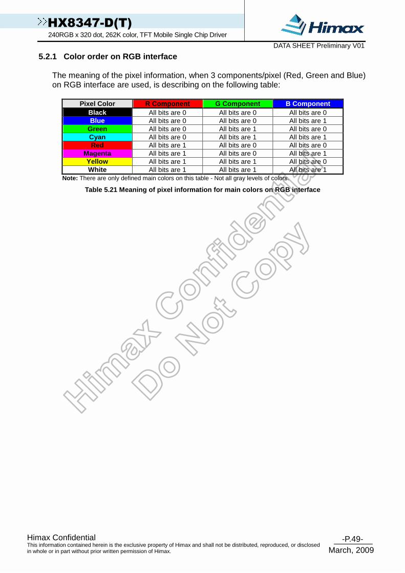
-P.49- Himax Confidential
March, 2009
This information contained herein is the exclusive property of Himax and shall not be distributed, reproduced, or disclosed in whole or in part without prior written permission of Himax.
HX8347-D(T) 240RGB x 320 dot, 262K color, TFT Mobile Single Chip Driver DATA SHEET Preliminary V01
5.2.1 Color order on RGB interface
The meaning of the pixel information, when 3 components/pixel (Red, Green and Blue) on RGB interface are used, is describing on the following table:
Pixel Color R Component G Component B Component
Black All bits are 0 All bits are 0 All bits are 0 Blue All bits are 0 All bits are 0 All bits are 1
Green All bits are 0 All bits are 1 All bits are 0 Cyan All bits are 0 All bits are 1 All bits are 1 Red All bits are 1 All bits are 0 All bits are 0
Magenta All bits are 1 All bits are 0 All bits are 1 Yellow All bits are 1 All bits are 1 All bits are 0 White All bits are 1 All bits are 1 All bits are 1
Note: There are only defined main colors on this table - Not all gray levels of colors.
Table 5.21 Meaning of pixel information for main co lors on RGB interface
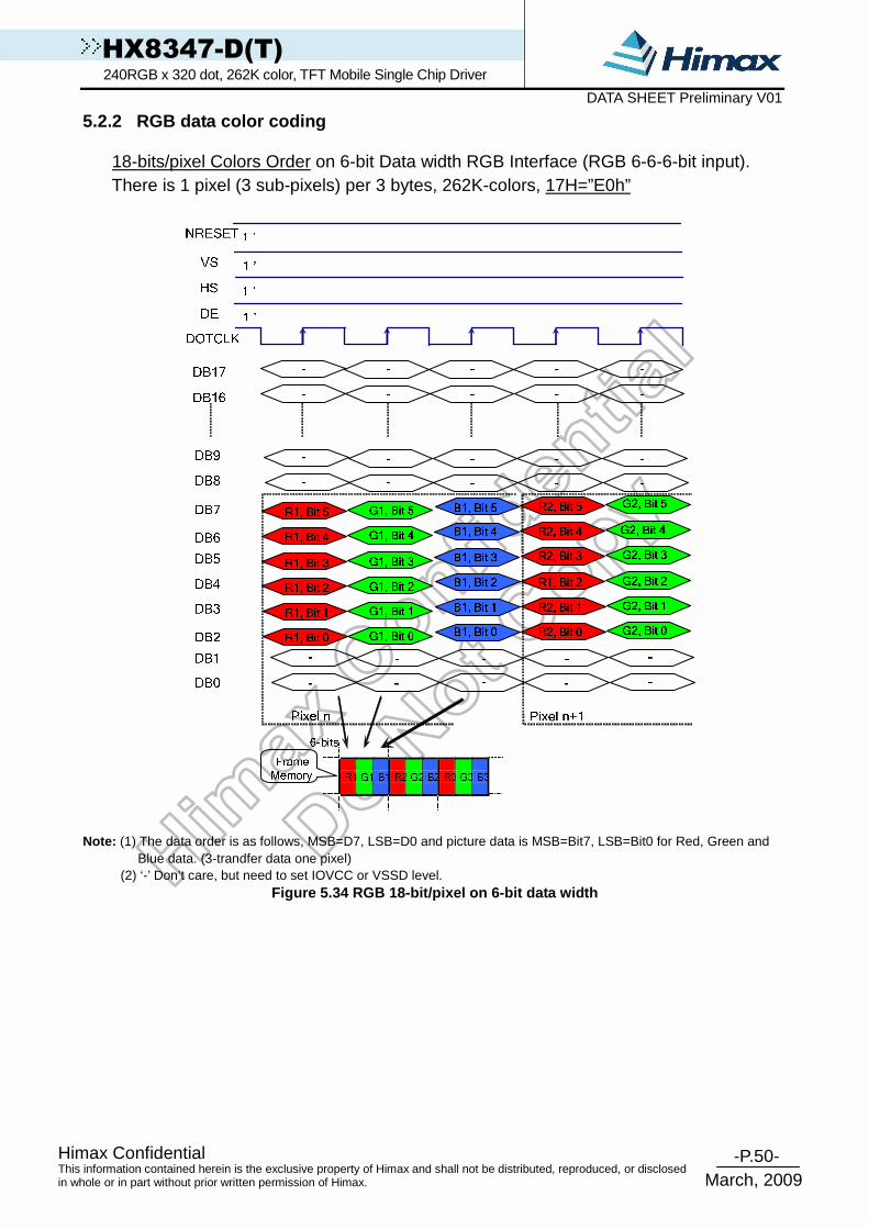
-P.50- Himax Confidential
March, 2009
This information contained herein is the exclusive property of Himax and shall not be distributed, reproduced, or disclosed in whole or in part without prior written permission of Himax.
HX8347-D(T) 240RGB x 320 dot, 262K color, TFT Mobile Single Chip Driver DATA SHEET Preliminary V01
5.2.2 RGB data color coding
18-bits/pixel Colors Order on 6-bit Data width RGB Interface (RGB 6-6-6-bit input). There is 1 pixel (3 sub-pixels) per 3 bytes, 262K-colors, 17H=”E0h”
Note: (1) The data order is as follows, MSB=D7, LSB=D0 and picture data is MSB=Bit7, LSB=Bit0 for Red, Green and
Blue data. (3-trandfer data one pixel) (2) ‘-’ Don’t care, but need to set IOVCC or VSSD level.
Figure 5.34 RGB 18-bit/pixel on 6-bit data width
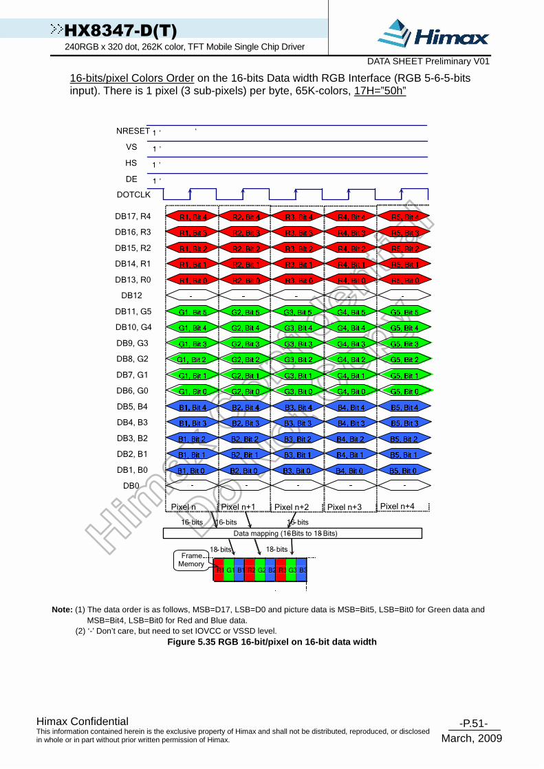
-P.51- Himax Confidential
March, 2009
This information contained herein is the exclusive property of Himax and shall not be distributed, reproduced, or disclosed in whole or in part without prior written permission of Himax.
HX8347-D(T) 240RGB x 320 dot, 262K color, TFT Mobile Single Chip Driver DATA SHEET Preliminary V01
16-bits/pixel Colors Order on the 16-bits Data width RGB Interface (RGB 5-6-5-bits input). There is 1 pixel (3 sub-pixels) per byte, 65K-colors, 17H=”50h”
NRESET ‘1 ’ ‘
VS ‘1 ’
DE ‘1 ’
HS ‘1 ’
DOTCLK
DB17, R4
DB16, R3
DB15, R2
DB14, R1
DB13, R0
DB12
Pixel n
DB11, G5
DB10, G4
DB9, G3
DB8, G2
DB7, G1
DB6, G0
DB5, B4
DB4, B3
DB3, B2
DB2, B1
DB1, B0
DB0
R1 G1 B1 R2 G2 B2 R3 G3 B3
Frame Memory
16-bits 16-bits 16-bits
Data mapping (16- Bits to 18-Bits)
18-bits 18-bits
Pixel n+1 Pixel n+2 Pixel n+3 Pixel n+4
Note: (1) The data order is as follows, MSB=D17, LSB=D0 and picture data is MSB=Bit5, LSB=Bit0 for Green data and
MSB=Bit4, LSB=Bit0 for Red and Blue data. (2) ‘-’ Don’t care, but need to set IOVCC or VSSD level.
Figure 5.35 RGB 16-bit/pixel on 16-bit data width

-P.52- Himax Confidential
March, 2009
This information contained herein is the exclusive property of Himax and shall not be distributed, reproduced, or disclosed in whole or in part without prior written permission of Himax.
HX8347-D(T) 240RGB x 320 dot, 262K color, TFT Mobile Single Chip Driver DATA SHEET Preliminary V01
18-bits/pixel Colors Order on the 18-bit Data width RGB Interface (RGB 6-6-6-bit input). There is 1 pixel (3 sub-pixels) per byte, 262K-colors, 17H=”60h”
Note: (1) The data order is as follows, MSB=D17, LSB=D0 and picture data is MSB=Bit5, LSB=Bit0 for Red, Green and
Blue data. (2) ‘-’ Don’t care, but need to set IOVCC or VSSD level.
Figure 5.36 RGB 18-bit/pixel on 18-bit data width

-P.53- Himax Confidential
March, 2009
This information contained herein is the exclusive property of Himax and shall not be distributed, reproduced, or disclosed in whole or in part without prior written permission of Himax.
HX8347-D(T) 240RGB x 320 dot, 262K color, TFT Mobile Single Chip Driver DATA SHEET Preliminary V01
6. Display Data GRAM
The display data RAM stores display dots and consists of 1,382,400 bits (240x18x320 bits). There is no restriction on access to the RAM even when the display data on the same address is loaded to DAC. There will be no abnormal visible effect on the display when there is a simultaneous Panel Read and Interface Read or Write to the same location of the Frame Memory.
6.1 Display data GRAM mapping
Every pixel (18-bit) data in GRAM is located by a (Page, Column) address (Y, X). By specifying the arbitrary window address SC, EC bits and SP, EP bits, it is possible to access the GRAM by setting RAMWR or RAMRD commands from start positions of the window address.
(00,00)H (00,01)H (00,02)H --------- (00,EC)H (00,ED)H (00,EE)H (00,EF)H (01,00)H (01,01)H (01,02)H --------- (01,EC)H (01,ED)H (01,EE)H (01,EF)H (02,00)H (02,01)H (02,02)H --------- (02,EC)H (02,ED)H (02,EE)H (02,EF)H (03,00)H (03,01)H (03,02)H --------- (03,EC)H (03,ED)H (03,EE)H (03,EF)H (04,00)H (04,01)H (04,02)H --------- (04,EC)H (04,ED)H (04,EE)H (04,EF)H (05,00)H (05,01)H (05,02)H --------- (05,EC)H (05,ED)H (05,EE)H (05,EF)H
--------
--------
--------
---------
--------
--------
--------
--------
(13A,00)H (13A,01)H (13A,02)H --------- (13A,EC)H (13A,ED)H (13A,EE)H (13A,EF)H (13B,00)H (13B,01)H (13B,02)H --------- (13B,EC)H (13B,ED)H (13B,EE)H (13B,EF)H (13C,00)H (13C,01)H (13C,02)H --------- (13C,EC)H (13C,ED)H (13C,EE)H (13C,EF)H (13D,00)H (13D,01)H (13D,02)H --------- (13D,EC)H (13DED)H (13D17E)H (13D,EF)H (13E,00)H (13E,01)H (13E,02)H --------- (13E,EC)H (13E,ED)H (13E,EE)H (13E,EF)H (13F,00)H (13F,01)H (13F,02)H --------- (13F,EC)H (13F,ED)H (13F,EE)H (13F,EF)H
Table 6.1 GRAM address for display panel position
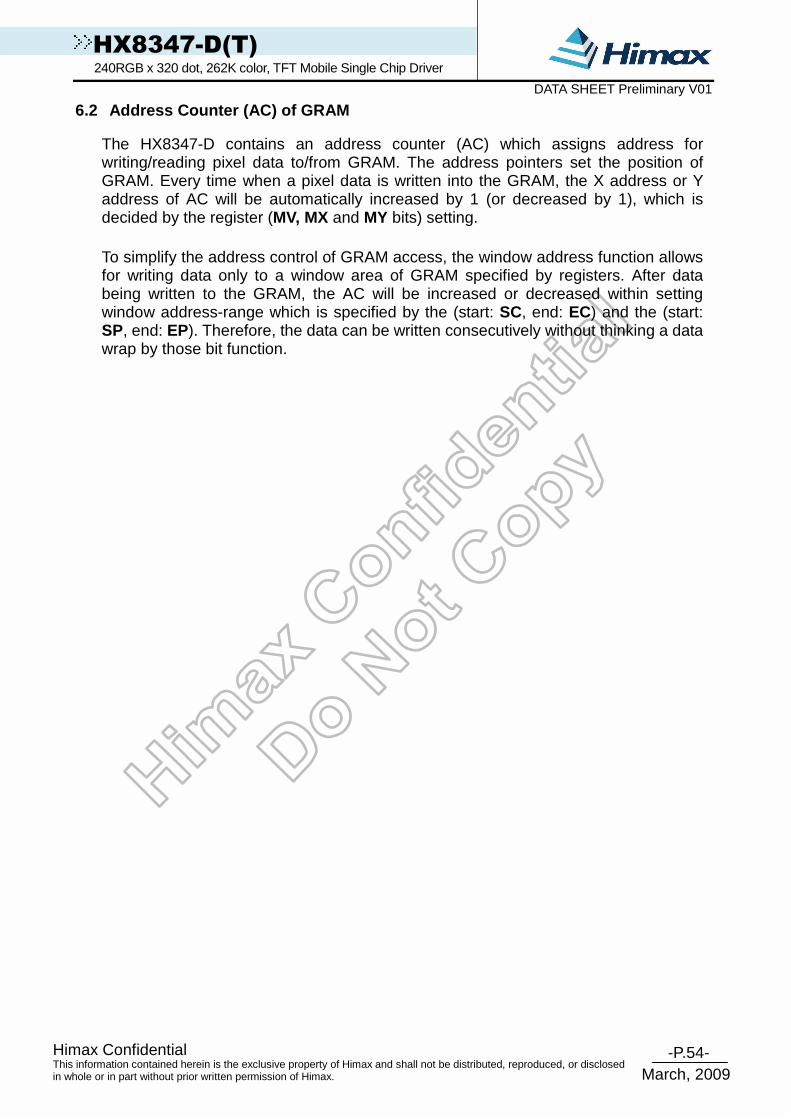
-P.54- Himax Confidential
March, 2009
This information contained herein is the exclusive property of Himax and shall not be distributed, reproduced, or disclosed in whole or in part without prior written permission of Himax.
HX8347-D(T) 240RGB x 320 dot, 262K color, TFT Mobile Single Chip Driver DATA SHEET Preliminary V01
6.2 Address Counter (AC) of GRAM The HX8347-D contains an address counter (AC) which assigns address for writing/reading pixel data to/from GRAM. The address pointers set the position of GRAM. Every time when a pixel data is written into the GRAM, the X address or Y address of AC will be automatically increased by 1 (or decreased by 1), which is decided by the register (MV, MX and MY bits) setting. To simplify the address control of GRAM access, the window address function allows for writing data only to a window area of GRAM specified by registers. After data being written to the GRAM, the AC will be increased or decreased within setting window address-range which is specified by the (start: SC, end: EC) and the (start: SP, end: EP). Therefore, the data can be written consecutively without thinking a data wrap by those bit function.
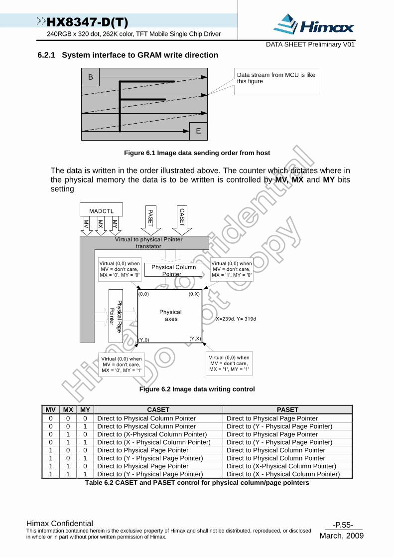
-P.55- Himax Confidential
March, 2009
This information contained herein is the exclusive property of Himax and shall not be distributed, reproduced, or disclosed in whole or in part without prior written permission of Himax.
HX8347-D(T) 240RGB x 320 dot, 262K color, TFT Mobile Single Chip Driver DATA SHEET Preliminary V01
6.2.1 System interface to GRAM write direction
B
E
Data stream from MCU is likethis figure
Figure 6.1 Image data sending order from host
The data is written in the order illustrated above. The counter which dictates where in the physical memory the data is to be written is controlled by MV, MX and MY bits setting
MADCTL
Physical Column
PointerPhysica
l Page
Pointe
r
CASET
PASET
MV
MX
MY
Physical
axes
Virtual to physical Pointer
transtator
Virtual (0,0) when
MV = don't care,
MX = '0', MY = '0'
(0,0) (0,X)
Virtual (0,0) when
MV = don't care,
MX = '1', MY = '0'
Virtual (0,0) when MV = don't care,
MX = '0', MY = '1'
(Y,0) (Y,X)
Virtual (0,0) when
MV = don't care,
MX = '1', MY = '1'
X=239d, Y= 319d
Figure 6.2 Image data writing control
MV MX MY CASET PASET 0 0 0 Direct to Physical Column Pointer Direct to Physical Page Pointer 0 0 1 Direct to Physical Column Pointer Direct to (Y - Physical Page Pointer) 0 1 0 Direct to (X-Physical Column Pointer) Direct to Physical Page Pointer 0 1 1 Direct to (X - Physical Column Pointer) Direct to (Y - Physical Page Pointer) 1 0 0 Direct to Physical Page Pointer Direct to Physical Column Pointer 1 0 1 Direct to (Y - Physical Page Pointer) Direct to Physical Column Pointer 1 1 0 Direct to Physical Page Pointer Direct to (X-Physical Column Pointer) 1 1 1 Direct to (Y - Physical Page Pointer) Direct to (X - Physical Column Pointer)
Table 6.2 CASET and PASET control for physical colu mn/page pointers
-P.56- Himax Confidential
March, 2009
This information contained herein is the exclusive property of Himax and shall not be distributed, reproduced, or disclosed in whole or in part without prior written permission of Himax.
HX8347-D(T) 240RGB x 320 dot, 262K color, TFT Mobile Single Chip Driver DATA SHEET Preliminary V01
For each image orientation, the controls for the column and page counters apply as below:
Condition Column Counter Page Counter
When RAMWR/RAMRD command is accepted. Return to “Start Column”
Return to “Start Page”
Complete Pixel Pair Write/Read action Increment by 1 No change
The Column counter value is larger than “End column.” Return to
“Start Column” Increment by 1
The Page counter value is larger than “End page”. Return to
“Start Column” Return to
“Start Page” Note: Data is always written to the Frame Memory in the same order, regardless of the Memory Write Direction
set by MX, MY, MV. Table 6.3 Rules for updating GRAM rrder
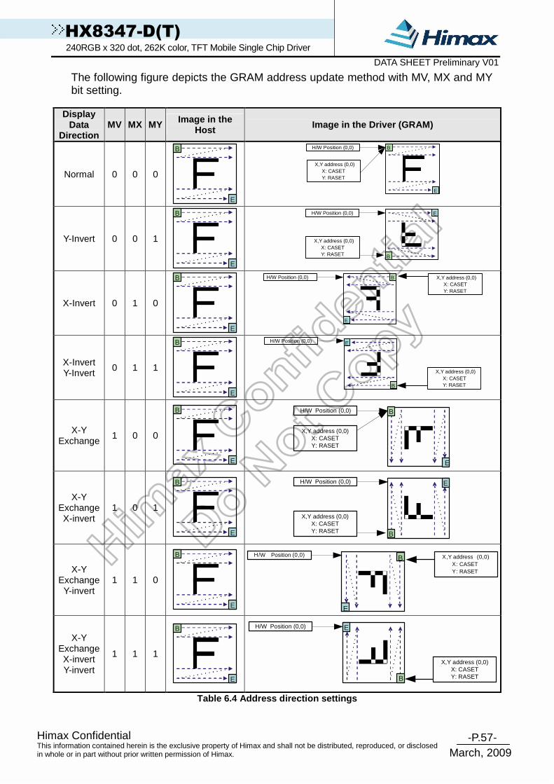
-P.57- Himax Confidential
March, 2009
This information contained herein is the exclusive property of Himax and shall not be distributed, reproduced, or disclosed in whole or in part without prior written permission of Himax.
HX8347-D(T) 240RGB x 320 dot, 262K color, TFT Mobile Single Chip Driver DATA SHEET Preliminary V01
The following figure depicts the GRAM address update method with MV, MX and MY bit setting.
Display Data
Direction MV MX MY Image in the
Host Image in the Driver (GRAM)
Normal 0 0 0
B
E
Y-Invert 0 0 1
B
E
X-Invert 0 1 0
B
E
X-Invert Y-Invert
0 1 1
B
E
X-Y Exchange
1 0 0
B
E
X,Y address (0,0)X: CASETY: RASET
B
E
H/W Position (0,0)
X-Y Exchange X-invert
1 0 1
B
E
X,Y address (0,0)X: CASETY: RASET
H/W Position (0,0)
B
E
X-Y Exchange Y-invert
1 1 0
B
E
X-Y Exchange X-invert Y-invert
1 1 1
B
E
X,Y address (0,0)X: CASETY: RASET
H/W Position (0,0)
B
E
Table 6.4 Address direction settings
H/W Position (0,0)
X,Y address (0,0)X: CASET Y: RASET
B
E
H/W Position (0,0)
X,Y address (0,0) X: CASET Y: RASET B
E
B
E
H/W Position (0,0) X,Y address (0,0) X: CASET Y: RASET
H/W Position (0,0)
B
E
X,Y address (0,0) X: CASET Y: RASET
X ,Y address ( 0, 0)X : CASET Y : RASET
H /W Position (0, 0) B
E

-P.58- Himax Confidential
March, 2009
This information contained herein is the exclusive property of Himax and shall not be distributed, reproduced, or disclosed in whole or in part without prior written permission of Himax.
HX8347-D(T) 240RGB x 320 dot, 262K color, TFT Mobile Single Chip Driver DATA SHEET Preliminary V01
Example for rotation with MY, MX and MV This example is using following values: start page = 0, end page = 40, start column = 0 and end column = 20 => commands: page address set (0, 40) and column address set (0, 20). The sent figure is as follows and its sending order is as follows.
Written image and direction from the host to frame memory
Start
End
Writieg direction Image from the host
Start page=0
End page=40
Start column =0 End column=20
Image position on the frame memory with MY
MemoryLocation
(0,0) FRAME
MEMORY
= 0/1 , MX = 0/1, MV = 0/1
MY =0MX =0MV =0
MemoryLocation
(0,0) FRAME
MEMORY
MY =0MX =1MV =0
MemoryLocation
(0,0) FRAME
MEMORY
MY =1MX =0MV =0
MemoryLocation
(0,0) FRAME
MEMORY
MY =1MX =1MV =0
Figure 6.3 Example for rotation with MY, MX and MV - 1
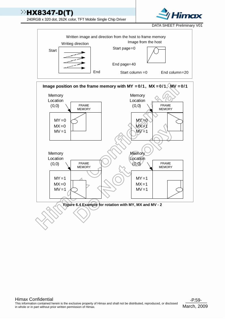
-P.59- Himax Confidential
March, 2009
This information contained herein is the exclusive property of Himax and shall not be distributed, reproduced, or disclosed in whole or in part without prior written permission of Himax.
HX8347-D(T) 240RGB x 320 dot, 262K color, TFT Mobile Single Chip Driver DATA SHEET Preliminary V01
Written image and direction from the host to frame memory
Start
End
Writieg direction Image from the host
Start page=0
End page=40
Start column =0 End column=20
Image position on the frame memory with MY
MemoryLocation
(0,0) FRAME
MEMORY
= 0/1 , MX = 0/1, MV = 0/1
MY =0MX =0MV =1
MemoryLocation
(0,0) FRAME
MEMORY
MY =0MX =1MV =1
MemoryLocation
(0,0) FRAME
MEMORY
MY =1MX =0MV =1
MemoryLocation
(0,0) FRAME
MEMORY
MY =1MX =1MV =1
Figure 6.4 Example for rotation with MY, MX and MV - 2

-P.60- Himax Confidential
March, 2009
This information contained herein is the exclusive property of Himax and shall not be distributed, reproduced, or disclosed in whole or in part without prior written permission of Himax.
HX8347-D(T) 240RGB x 320 dot, 262K color, TFT Mobile Single Chip Driver DATA SHEET Preliminary V01
6.3 GRAM to display address mapping By setting the SS bit, the relation between the source output channel and the GRAM address can be changed as reverse display. By setting the GS bit, the relation between the gate output channel and the GRAM address can be changed as reverse display. By setting the BGR bit, the relation between the source output channel and the <R>, <G>, <B> dot allocation can be reversed for different LCD color filter arrangement. Table 6.5, Table 6.6 and Table 6.7 show relations among the GRAM data allocation, the source output channel, and the R, G, B dot allocation.
SRGB = ‘H’
SMX = ‘1’ S1 S2 S3 S4 S5 S6 ------- S715 S716 S717 S718 S719 S720 Source Output SMX= ‘0’ S718 S719 S720 S715 S716 S717 ------- S4 S5 S6 S1 S2 S3
X Address “00”h “01”h ------- “EE”h “EF”h RGB data R G B R G B ------- R G B R G B
Pixel Pixel 1 Pixel 2 ------- Pixel 239 Pixel 240
SRGB = ‘L’ SMX = ‘1’ S3 S2 S1 S6 S5 S4 ------- S717 S716 S715 S720 S719 S718 Source
Output SMX = ‘0’ S720 S719 S718 S717 S716 S715 ------- S6 S5 S4 S3 S2 S1 X Address “00”h “01”h ------- “EE”h “EF”h
Bit Allocation R G B R G B ------- R G B R G B Pixel Pixel 1 Pixel 2 ------- Pixel 239 Pixel 240
Note: (1) RGB direction default setting is defined by the hardware pin SRGB. (2) Register R16h [3] (BGR) bit will override the hardware SRGB setting once software was sent to R16h [3] (BGR)
bit. Hardware pin SRGB control is invalid, and RGB filter order is controlled by R16h [3] (BGR) bit.
Table 6.5 GRAM X address and display panel position
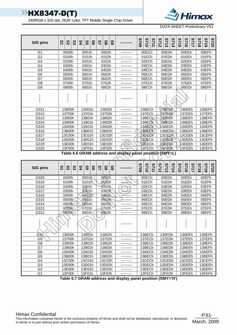
-P.61- Himax Confidential
March, 2009
This information contained herein is the exclusive property of Himax and shall not be distributed, reproduced, or disclosed in whole or in part without prior written permission of Himax.
HX8347-D(T) 240RGB x 320 dot, 262K color, TFT Mobile Single Chip Driver DATA SHEET Preliminary V01
S/G pins
S1
S2
S3
S4
S5
S6
S7
S8
S9 ---------
S709
S710
S711
S712
S713
S714
S715
S716
S717
S718
S719
S720
G1 0000h 0001h 0002h --------- 00ECh 00EDh 00EEh 00EFh G2 0100h 0101h 0102h --------- 01ECh 01EDh 01EEh 01EFh G3 0200h 0201h 0202h --------- 02ECh 02EDh 02EEh 02EFh G4 0300h 0301h 0302h --------- 03ECh 03EDh 03EEh 03EFh G5 0400h 0401h 0402h --------- 04ECh 04EDh 04EEh 04EFh G6 0500h 0501h 0502h --------- 05ECh 05EDh 05EEh 05EFh G7 0600h 0601h 0602h --------- 06ECh 06EDh 06EEh 06EFh G8 0700h 0701h 0702h --------- 07ECh 07EDh 07EEh 07EFh G9 0800h 0801h 0802h --------- 08ECh 08EDh 08EEh 08EFh
-------
-------
-------
-------
---------
-------
-------
-------
-------
G311 13600h 13601h 13602h --------- 136ECh 136EDh 136EEh 136EFh G312 13700h 13701h 13702h --------- 137ECh 137EDh 137EEh 137EFh G313 13800h 13801h 13802h --------- 138ECh 138EDh 138EEh 138EFh G314 13900h 13901h 13902h --------- 139ECh 139EDh 139EEh 139EFh G315 13A00h 13A01h 13A02h --------- 13AECh 13AEDh 13AEEh 13AEFh G316 13B00h 13B01h 13B02h --------- 13BECh 13BEDh 13BEEh 13BEFh G317 13C00h 13C01h 13C02h --------- 13CECh 13CEDh 13CEEh 13CEFh G318 13D00h 13D01h 13D02h --------- 13DECh 13DEDh 13DEEh 13DEFh G319 13E00h 13E01h 13E02h --------- 13EECh 13EEDh 13EEEh 13EEFh G320 13F00h 13F01h 13F02h --------- 13FECh 13FEDh 13FEEh 13FEFh
Table 6.6 GRAM address and display panel position ( SMY=L)
S/G pins
S
1
S2
S3
S4
S5
S6
S7
S8
S9 ---------
S709
S710
S711
S712
S713
S714
S715
S716
S717
S718
S719
S720
G320 0000h 0001h 0002h --------- 00ECh 00EDh 00EEh 00EFh G319 0100h 0101h 0102h --------- 01ECh 01EDh 01EEh 01EFh G318 0200h 0201h 0202h --------- 02ECh 02EDh 02EEh 02EFh G317 0300h 0301h 0302h --------- 03ECh 03EDh 03EEh 03EFh G316 0400h 0401h 0402h --------- 04ECh 04EDh 04EEh 04EFh G315 0500h 0501h 0502h --------- 05ECh 05EDh 05EEh 05EFh G314 0600h 0601h 0602h --------- 06ECh 06EDh 06EEh 06EFh G313 0700h 0701h 0702h --------- 07ECh 07EDh 07EEh 07EFh G312 0800h 0801h 0802h --------- 08ECh 08EDh 08EEh 08EFh
-------
-------
-------
-------
---------
-------
-------
-------
-------
G10 13600h 13601h 13602h --------- 136ECh 136EDh 136EEh 136EFh G9 13700h 13701h 13702h --------- 137ECh 137EDh 137EEh 137EFh G8 13800h 13801h 13802h --------- 138ECh 138EDh 138EEh 138EFh G7 13900h 13901h 13902h --------- 139ECh 139EDh 139EEh 139EFh G6 13A00h 13A01h 13A02h --------- 13AECh 13AEDh 13AEEh 13AEFh G5 13B00h 13B01h 13B02h --------- 13BECh 13BEDh 13BEEh 13BEFh G4 13C00h 13C01h 13C02h --------- 13CECh 13CEDh 13CEEh 13CEFh G3 13D00h 13D01h 13D02h --------- 13DECh 13DEDh 13DEEh 13DEFh G2 13E00h 13E01h 13E02h --------- 13EECh 13EEDh 13EEEh 13EEFh G1 13F00h 13F01h 13F02h --------- 13FECh 13FEDh 13FEEh 13FEFh
Table 6.7 GRAM address and display panel position ( SMY=’H’)

-P.62- Himax Confidential
March, 2009
This information contained herein is the exclusive property of Himax and shall not be distributed, reproduced, or disclosed in whole or in part without prior written permission of Himax.
HX8347-D(T) 240RGB x 320 dot, 262K color, TFT Mobile Single Chip Driver DATA SHEET Preliminary V01
HX8347-D supports three kinds of display mode: one is Normal Display Mode, one is the other is Partial Display Mode, and Scrolling Display Mode. When the PLTON = ‘0’ is set, HX8347-D will be into Normal Display Mode. When the PLTON = ‘1’ is set, HX8347-D will be into Partial Display Mode. When the SCROLL_ON = ‘1’ is set, HX8347-D will be into Scrolling Display Mode.
6.3.1 Normal display on or partial mode on, vertica l scroll off In this mode, content of the frame memory within an area where column pointer is 0000h to 00EFh and page pointer is 0000h to 013Fh is displayed. To display a dot on leftmost top corner, store the dot data at (column pointer, page pointer) = (0,0) (SMX = ‘L’, SMY = ‘L’).
11 13
21 22 23
31 32
14 1X
2X 2Y
3Y
1Y
X1 X2
Y3 Y1 Y2
XX XY
YX YY
01 03 04 0X 0Y05
Z1 Z2 Z3 Z4 ZV ZX ZYZ5
2Z
3Z
1Z
XZ
YZ
0Z
ZZ
10
20
30
X0
Y0
00
Z0
00h
01h
EEh
EFh
V1 VY VZV0
U1 UY UZU0EDh
02
12
W0 W1
YW
ZW
WY WZ
0W
1W
320 Lines
240 x 320 x 18 bit Frame Memory
11 13
21 22 23
31 32
14 1X
2X 2Y
3Y
1Y
X1 X2
Y3 Y1 Y2
XX XY
YX YY
01 03 04 0X 0Y05
Z1 Z2 Z3 Z4 ZV ZX ZYZ5
2Z
3Z
1Z
XZ
YZ
0Z
ZZ
10
20
30
X0
Y0
00
Z0
00h
0 0h
01h
0 1h
EEh
EFh
V1 VY VZV0
U1 UY UZU0
EDh
13Dh
02
12
W0 W1
13Eh
13Fh
YW
ZW
WY WZ
0W
1W320 Lines
240 x 320
LCD Panel
13Dh
13Eh
13Fh
00h
01h
240 Columns

-P.63- Himax Confidential
March, 2009
This information contained herein is the exclusive property of Himax and shall not be distributed, reproduced, or disclosed in whole or in part without prior written permission of Himax.
HX8347-D(T) 240RGB x 320 dot, 262K color, TFT Mobile Single Chip Driver DATA SHEET Preliminary V01
Example:
(1) PLTON = ‘1’,
(2) PSL [15:0] =11DEC, PEL [15:0] =130DEC, MADCTL’s B4(ML)=’0’ (SMY = ‘L’).
0
Display PanelDisplay PanelDisplay PanelDisplay Panel
*-- 123456789--*
Non- display Area
Non- display Area
320
0
11
130
320P
anel Scan
Direction
Physical 0, 0 Point
0
Content of GRAMContent of GRAMContent of GRAMContent of GRAM
*-- 123456789 --*
320
*-- ABCDEFG --*
Figure 6. 5 Partial Display Area Setting (ML=’0’)
Example:
(1) PLTON = ‘1’,
(2) PSL [15:0] =11DEC, PEL [15:0] =130DEC, MADCTL’s B4(ML)=’1’ (SMY = ‘L’).
0
Display PanelDisplay PanelDisplay PanelDisplay Panel
319
Physical 0, 0 Point
Content of GRAMContent of GRAMContent of GRAMContent of GRAM
319
****-------- 123456789123456789123456789123456789 --------****
****-------- ABCDEFGABCDEFGABCDEFGABCDEFG --------****
NonNonNonNon---- display Areadisplay Areadisplay Areadisplay Area
NonNonNonNon---- display Areadisplay Areadisplay Areadisplay Area
****-------- ABCDEFGABCDEFGABCDEFGABCDEFG--------****
0
11
130
319
Figure 6. 6 Partial Display Area Setting (ML=’1’)
The refresh gate scan cycle in the rest display area of the screen (non-display area) can be
specified by ISC[3:0] bits. The scan cycle is set to an odd number from 0~13.The polarity is
inverted every scan cycle.
ISC3 ISC2 ISC1 ISC0 Scan Cycle fFLM = 60Hz
0 0 0 0 1 frame 17ms 0 0 0 1 5 frames 84ms 0 0 1 0 9 frames 150ms : : : : : 1 1 0 1 53 frames 880ms 1 1 1 0 57 frames 946ms 1 1 1 1 Setting Inhibited -
Table 6. 1 ISC [3:0] Bits Definition The rest display area (non-display area) will be the white display if the type of LCD is normally
white (REV_panel = “0”) and will be the black display if the type of LCD is normally black
(REV_panel = “1”) in refresh gate scan cycle.
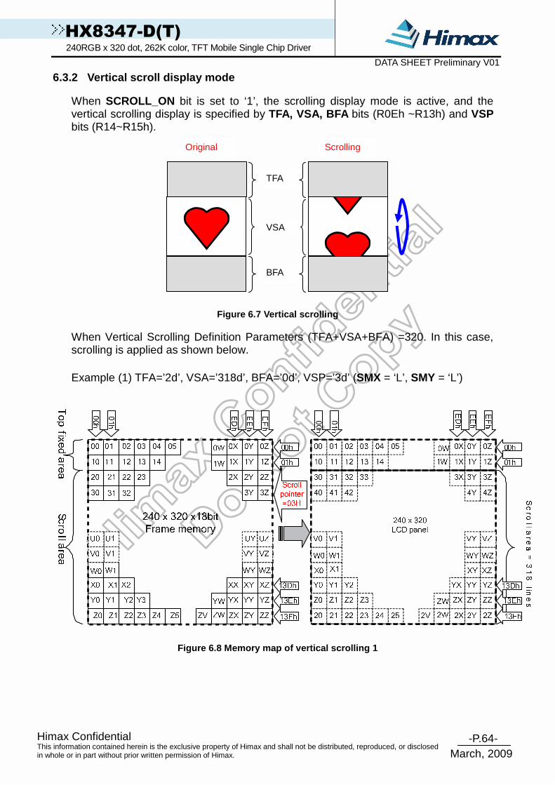
-P.64- Himax Confidential
March, 2009
This information contained herein is the exclusive property of Himax and shall not be distributed, reproduced, or disclosed in whole or in part without prior written permission of Himax.
HX8347-D(T) 240RGB x 320 dot, 262K color, TFT Mobile Single Chip Driver DATA SHEET Preliminary V01
6.3.2 Vertical scroll display mode
When SCROLL_ON bit is set to ‘1’, the scrolling display mode is active, and the vertical scrolling display is specified by TFA, VSA, BFA bits (R0Eh ~R13h) and VSP bits (R14~R15h).
Figure 6.7 Vertical scrolling
When Vertical Scrolling Definition Parameters (TFA+VSA+BFA) =320. In this case, scrolling is applied as shown below. Example (1) TFA=’2d’, VSA=’318d’, BFA=’0d’, VSP=’3d’ (SMX = ‘L’, SMY = ‘L’)
Figure 6.8 Memory map of vertical scrolling 1
Original Scrolling
TFA
VSA
BFA

-P.65- Himax Confidential
March, 2009
This information contained herein is the exclusive property of Himax and shall not be distributed, reproduced, or disclosed in whole or in part without prior written permission of Himax.
HX8347-D(T) 240RGB x 320 dot, 262K color, TFT Mobile Single Chip Driver DATA SHEET Preliminary V01
Example (2) TFA=’2d’, VSA=’316d’, BFA=’2d’, VSP=’3d’ (SMX = ‘L’, SMY = ‘L’)
Figure 6.9 Memory map of vertical scrolling 2
Example (3) TFA=’2d’, VSA=’316d’, BFA=’2d’, VSP=’5d’ (SMX = ‘L’, SMY = ‘L’).
11 12 13
21 22 23
31 32
14 1X
2X 2Y
3Y
1Y
X1 X2
Y3Y1 Y2
XX XY
YX YY
01 02 03 04 0X 0Y05
Z1 Z2 Z3 Z4 ZV ZX ZYZ5
2Z
3Z
1Z
XZ
YZ
0Z
ZZ
10
20
30
X0
Y0
00
Z0
00h
01h
V1 VY VZV0
U1 UY UZU0
13Dh
40 4Z
50
41
5Z
11 12 13
51 52 53
61 62
14 1X
5X 5Y
6Y
1Y
41 42 4X 4Y
01 02 03 04 0X 0Y05
5Z
6Z
1Z
4Z
0Z
10
50
60
40
00 00h
01h
Y3Y1 Y2 YX YY
Z1 Z2 Z3 Z4 ZV ZX ZYZ5
YZ
ZZ
Y0
Z0
3130
X1X0
3Y 3Z
XY XZ
240 x 320 x18bitFrame memory
240 x 320
LCD panel
W1W0
13Eh
13Fh
WY WZ
YW
ZW
0W
1W
13Dh
13Eh
13Fh
YW
ZW
20 21
0W
1W
Scrollpointer=05H
Figure 6.10 Memory map of vertical scrolling 3

-P.66- Himax Confidential
March, 2009
This information contained herein is the exclusive property of Himax and shall not be distributed, reproduced, or disclosed in whole or in part without prior written permission of Himax.
HX8347-D(T) 240RGB x 320 dot, 262K color, TFT Mobile Single Chip Driver DATA SHEET Preliminary V01
Vertical scroll example There are 2 types of vertical scrolling, which are determined by the TFA, VSA, BFA bits (R0Eh ~R13h) and VSP bits (R14~R15h). Case 1: TFA + VSA + BFA ≠ ‘320d’ N/A. Do not set TFA + VSA + BFA ≠ ‘320d’. In that case, unexpected picture will be shown. Case 2: TFA + VSA + BFA = ‘320d’ (Scrolling) Example (1) When TFA=’0d’, VSA=’320d’, BFA=’0d’ and VSP=’40d’ (SMX = ‘L’, SMY = ‘L’)
V S P
P h y s ic a l L in e P o in te r
21
21
D is p la y
In c re m e n t V S P
V S P
P h y s ic a l L in e P o in te r
21 2
1
D is p la y
D is p la y A x is (0 ,0 )
M e m o ry P h y s ic a l A x is (0 ,0 )
D is p la y A x is (0 ,0 )
F ra m e
F ra m e M e m o ry
M e m o ry Figure 6.11 Vertical scrolling example
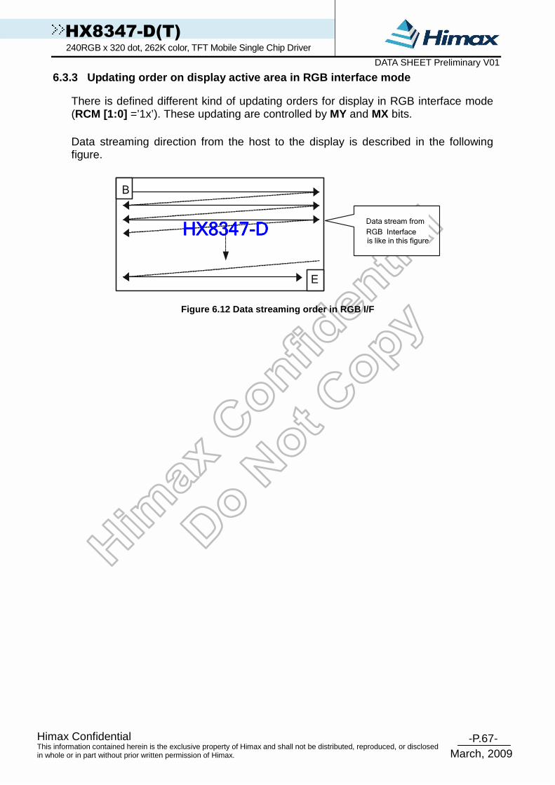
-P.67- Himax Confidential
March, 2009
This information contained herein is the exclusive property of Himax and shall not be distributed, reproduced, or disclosed in whole or in part without prior written permission of Himax.
HX8347-D(T) 240RGB x 320 dot, 262K color, TFT Mobile Single Chip Driver DATA SHEET Preliminary V01
6.3.3 Updating order on display active area in RGB interface mode
There is defined different kind of updating orders for display in RGB interface mode (RCM [1:0] =’1x’). These updating are controlled by MY and MX bits. Data streaming direction from the host to the display is described in the following figure.
B
E
Data stream from
RGB Interfaceis like in this figure
HXHXHXHX8347834783478347----DDDD
Figure 6.12 Data streaming order in RGB I/F
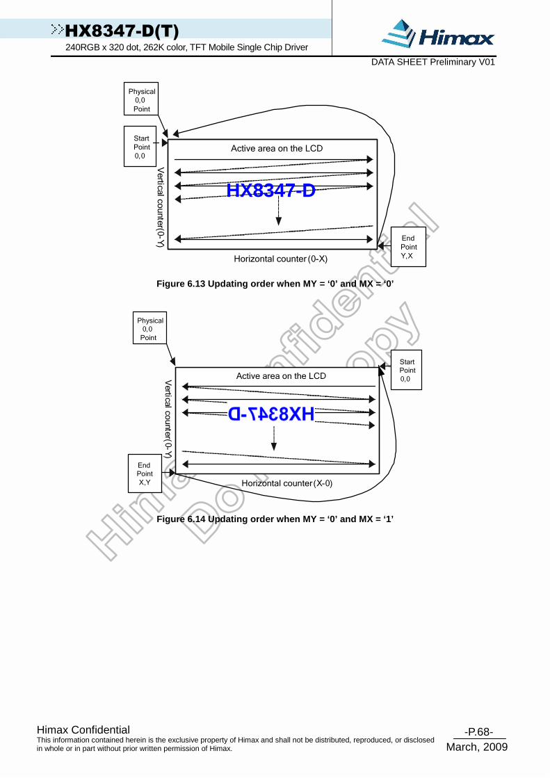
-P.68- Himax Confidential
March, 2009
This information contained herein is the exclusive property of Himax and shall not be distributed, reproduced, or disclosed in whole or in part without prior written permission of Himax.
HX8347-D(T) 240RGB x 320 dot, 262K color, TFT Mobile Single Chip Driver DATA SHEET Preliminary V01
Active area on the LCD
End
Point
Y,X
Start
Point
0,0
Vertic
alcounter(0
-Y)
Horizontal counter (0-X)
Physical0,0
Point
HX8347-D
Figure 6.13 Updating order when MY = ‘0’ and MX = ‘ 0’
Active area on the LCDVertica
lcounter(0
-Y)
Horizontal counter (X-0)
Physical
0,0
Point
Start
Point
0,0
End
Point
Y,X
Figure 6.14 Updating order when MY = ‘0’ and MX = ‘ 1’
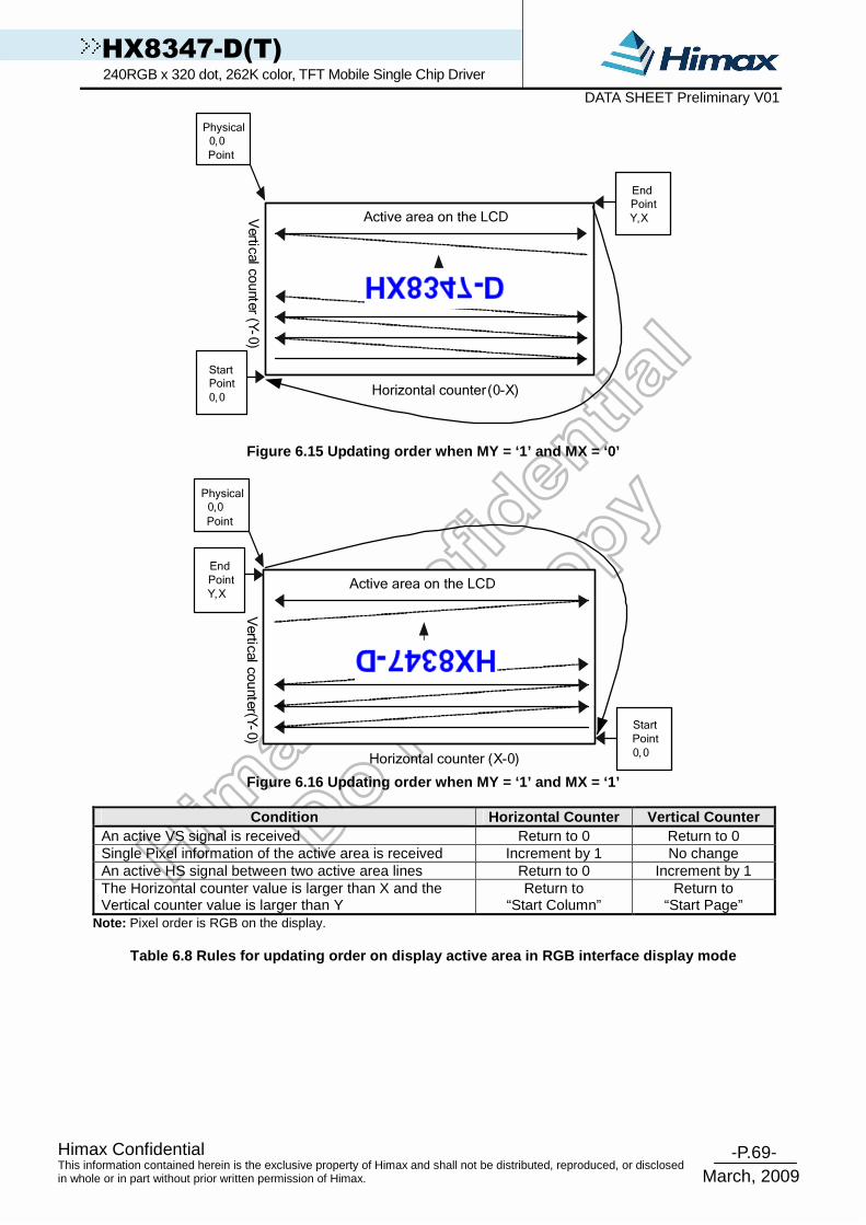
-P.69- Himax Confidential
March, 2009
This information contained herein is the exclusive property of Himax and shall not be distributed, reproduced, or disclosed in whole or in part without prior written permission of Himax.
HX8347-D(T) 240RGB x 320 dot, 262K color, TFT Mobile Single Chip Driver DATA SHEET Preliminary V01
Active area on the LCD
End
Point
Y,XVertic
alcounter(Y-0)
Horizontal counter (0-X)
Physical
0,0
Point
StartPoint
0,0
Figure 6.15 Updating order when MY = ‘1’ and MX = ‘ 0’
Active area on the LCD
Vertic
alcounter(Y
-0)
Horizontal counter (X-0)
Physical0,0
Point
Start
Point
0,0
End
Point
Y,X
Figure 6.16 Updating order when MY = ‘1’ and MX = ‘ 1’
Condition Horizontal Counter Vertical Counter
An active VS signal is received Return to 0 Return to 0 Single Pixel information of the active area is received Increment by 1 No change An active HS signal between two active area lines Return to 0 Increment by 1 The Horizontal counter value is larger than X and the Vertical counter value is larger than Y
Return to “Start Column”
Return to “Start Page”
Note: Pixel order is RGB on the display.
Table 6.8 Rules for updating order on display activ e area in RGB interface display mode
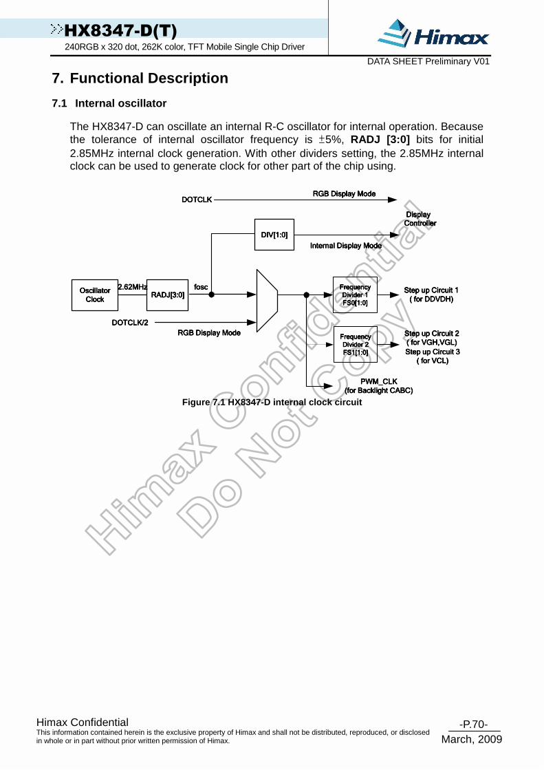
-P.70- Himax Confidential
March, 2009
This information contained herein is the exclusive property of Himax and shall not be distributed, reproduced, or disclosed in whole or in part without prior written permission of Himax.
HX8347-D(T) 240RGB x 320 dot, 262K color, TFT Mobile Single Chip Driver DATA SHEET Preliminary V01
7. Functional Description 7.1 Internal oscillator
The HX8347-D can oscillate an internal R-C oscillator for internal operation. Because the tolerance of internal oscillator frequency is ±5%, RADJ [3:0] bits for initial 2.85MHz internal clock generation. With other dividers setting, the 2.85MHz internal clock can be used to generate clock for other part of the chip using.
Internal Display ModeInternal Display ModeInternal Display ModeInternal Display Mode
foscfoscfoscfosc
RGB Display ModeRGB Display ModeRGB Display ModeRGB Display Mode
OscillatorOscillatorOscillatorOscillator
ClockClockClockClock
DOTCLKDOTCLKDOTCLKDOTCLK
Frequency Frequency Frequency Frequency
Divider Divider Divider Divider 1111
FSFSFSFS0000[[[[1111::::0000]]]]
Step up Circuit Step up Circuit Step up Circuit Step up Circuit 1111
( ( ( ( for DDVDHfor DDVDHfor DDVDHfor DDVDH))))
DIVDIVDIVDIV[[[[1111::::0000]]]]
PWMPWMPWMPWM____CLKCLKCLKCLK
((((for Backlight CABCfor Backlight CABCfor Backlight CABCfor Backlight CABC))))
2222....62626262MHzMHzMHzMHz
Frequency Frequency Frequency Frequency
Divider Divider Divider Divider 2222
FSFSFSFS1111[[[[1111::::0000]]]]
Step up Circuit Step up Circuit Step up Circuit Step up Circuit 2222
( ( ( ( for VGHfor VGHfor VGHfor VGH,,,,VGLVGLVGLVGL))))
DisplayDisplayDisplayDisplayControllerControllerControllerController
RADJRADJRADJRADJ[[[[3333::::0000]]]]
Step up Circuit Step up Circuit Step up Circuit Step up Circuit 3333
( ( ( ( for VCLfor VCLfor VCLfor VCL))))
DOTCLKDOTCLKDOTCLKDOTCLK////2222
RGB Display ModeRGB Display ModeRGB Display ModeRGB Display Mode
Figure 7.1 HX8347-D internal clock circuit
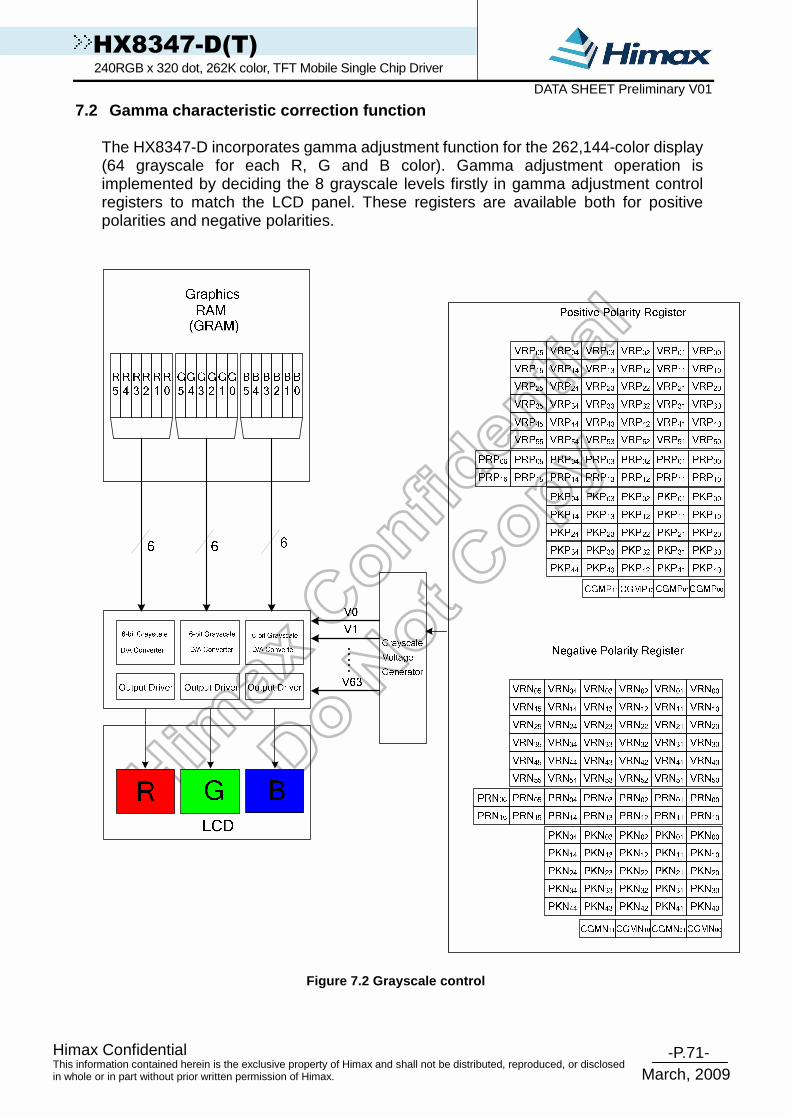
-P.71- Himax Confidential
March, 2009
This information contained herein is the exclusive property of Himax and shall not be distributed, reproduced, or disclosed in whole or in part without prior written permission of Himax.
HX8347-D(T) 240RGB x 320 dot, 262K color, TFT Mobile Single Chip Driver DATA SHEET Preliminary V01
7.2 Gamma characteristic correction function The HX8347-D incorporates gamma adjustment function for the 262,144-color display (64 grayscale for each R, G and B color). Gamma adjustment operation is implemented by deciding the 8 grayscale levels firstly in gamma adjustment control registers to match the LCD panel. These registers are available both for positive polarities and negative polarities.
Figure 7.2 Grayscale control
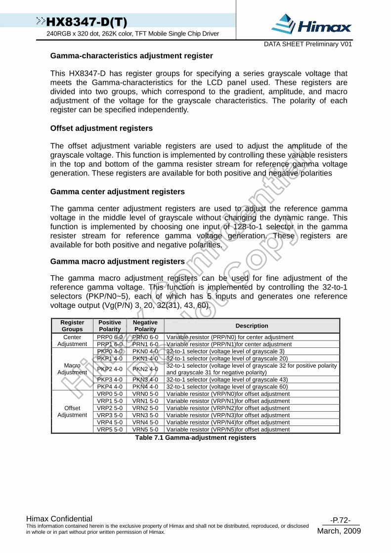
-P.72- Himax Confidential
March, 2009
This information contained herein is the exclusive property of Himax and shall not be distributed, reproduced, or disclosed in whole or in part without prior written permission of Himax.
HX8347-D(T) 240RGB x 320 dot, 262K color, TFT Mobile Single Chip Driver DATA SHEET Preliminary V01
Gamma-characteristics adjustment register This HX8347-D has register groups for specifying a series grayscale voltage that meets the Gamma-characteristics for the LCD panel used. These registers are divided into two groups, which correspond to the gradient, amplitude, and macro adjustment of the voltage for the grayscale characteristics. The polarity of each register can be specified independently. Offset adjustment registers The offset adjustment variable registers are used to adjust the amplitude of the grayscale voltage. This function is implemented by controlling these variable resisters in the top and bottom of the gamma resister stream for reference gamma voltage generation. These registers are available for both positive and negative polarities Gamma center adjustment registers The gamma center adjustment registers are used to adjust the reference gamma voltage in the middle level of grayscale without changing the dynamic range. This function is implemented by choosing one input of 128-to-1 selector in the gamma resister stream for reference gamma voltage generation. These registers are available for both positive and negative polarities. Gamma macro adjustment registers The gamma macro adjustment registers can be used for fine adjustment of the reference gamma voltage. This function is implemented by controlling the 32-to-1 selectors (PKP/N0~5), each of which has 5 inputs and generates one reference voltage output (Vg(P/N) 3, 20, 32(31), 43, 60).
Register Groups
Positive Polarity
Negative Polarity Description
PRP0 6-0 PRN0 6-0 Variable resistor (PRP/N0) for center adjustment Center Adjustment PRP1 6-0 PRN1 6-0 Variable resistor (PRP/N1)for center adjustment
PKP0 4-0 PKN0 4-0 32-to-1 selector (voltage level of grayscale 3) PKP1 4-0 PKN1 4-0 32-to-1 selector (voltage level of grayscale 20)
PKP2 4-0 PKN2 4-0 32-to-1 selector (voltage level of grayscale 32 for positive polarity and grayscale 31 for negative polarity)
PKP3 4-0 PKN3 4-0 32-to-1 selector (voltage level of grayscale 43)
Macro Adjustment
PKP4 4-0 PKN4 4-0 32-to-1 selector (voltage level of grayscale 60) VRP0 5-0 VRN0 5-0 Variable resistor (VRP/N0)for offset adjustment VRP1 5-0 VRN1 5-0 Variable resistor (VRP/N1)for offset adjustment VRP2 5-0 VRN2 5-0 Variable resistor (VRP/N2)for offset adjustment VRP3 5-0 VRN3 5-0 Variable resistor (VRP/N3)for offset adjustment VRP4 5-0 VRN4 5-0 Variable resistor (VRP/N4)for offset adjustment
Offset Adjustment
VRP5 5-0 VRN5 5-0 Variable resistor (VRP/N5)for offset adjustment Table 7.1 Gamma-adjustment registers

-P.73- Himax Confidential
March, 2009
This information contained herein is the exclusive property of Himax and shall not be distributed, reproduced, or disclosed in whole or in part without prior written permission of Himax.
HX8347-D(T) 240RGB x 320 dot, 262K color, TFT Mobile Single Chip Driver DATA SHEET Preliminary V01
Gamma resister stream The block consists of two gamma resister streams one is for positive polarity and the other is for negative polarity, each one including eight gamma reference voltages. VgP/N (0, 1, 2, 3, 8 20, 32(31), 43, 55, 60, 61, 62, 63). Furthermore, the block has a pin (VGS) to connect a variable resistor outside the chip for the variation between panels, if needed.
Figure 7.3 Gamma resister stream and gamma referenc e voltage

-P.74- Himax Confidential
March, 2009
This information contained herein is the exclusive property of Himax and shall not be distributed, reproduced, or disclosed in whole or in part without prior written permission of Himax.
HX8347-D(T) 240RGB x 320 dot, 262K color, TFT Mobile Single Chip Driver DATA SHEET Preliminary V01
Variable resister There are two types of variable resistors, one is for center adjustment and the other is for offset adjustment. The resistances are decided by setting values in the center adjustment, offset adjustment registers. Their relationships are shown below.
Value in Register
VR(P/N)0 5-0 Resistance VR(P/N)0
Value in Register VR(P/N)1 5-0
Resistance VR(P/N)1 Value in Register
VR(P/N)2 5-0 Resistance VR(P/N)2
000000 0R 000000 0R 000000 0R 000001 20R 000001 2R 000001 2R 000010 22R 000010 4R 000010 4R 000011 24R 000011 6R 000011 6R
• •
• •
• •
• •
• •
• •
011101 76R 011101 58R 011101 58R 011110 78R 011110 60R 011110 60R 011111 80R 011111 62R 011111 62R 100000 84R 100000 66R 100000 66R 100001 88R 100001 70R 100001 70R 100010 92R 100010 74R 100010 74R
• •
• •
• •
• •
• •
• •
111101 200R 111101 182R 111101 182R 111110 204R 111110 186R 111110 186R 111111 208R 111111 190R 111111 190R
Value in Register
VR(P/N)3 5-0 Resistance VR(P/N)3
Value in Register VR(P/N)4 5-0
Resistance VR(P/N)4 Value in Register
VR(P/N)5 5-0 Resistance VR(P/N)2
000000 0R 000000 0R 000000 0R 000001 4R 000001 4R 000001 4R 000010 8R 000010 8R 000010 8R
• •
• •
• •
• •
• •
• •
011101 116R 011101 116R 011101 116R 011110 120R 011110 120R 011110 120R 011111 124R 011111 124R 011111 124R 100000 128R 100000 128R 100000 128R 100001 130R 100001 130R 100001 130R 100010 132R 100010 132R 100010 132R
• •
• •
• •
• •
• •
• •
111100 184R 111100 184R 111100 184R 111101 186R 111101 186R 111101 186R 111110 188R 111110 188R 111110 188R 111111 190R 111111 190R 111111 208R
Table 7.2 Offset adjustment 0 ~ 5
Value in Register PR(P/N)0 6-0
Resistance PR(P/N)0
Value in Register PR(P/N)1 6-0
Resistance PR(P/N)1
0000000 0R 0000000 0R 0000001 2R 0000001 2R 0000010 4R 0000010 4R
• •
• •
• •
• •
1111101 250R 1010101 250R 1111110 252R 1111110 252R 1111111 254R 1111111 254R
Table 7.3 Center adjustment

-P.75- Himax Confidential
March, 2009
This information contained herein is the exclusive property of Himax and shall not be distributed, reproduced, or disclosed in whole or in part without prior written permission of Himax.
HX8347-D(T) 240RGB x 320 dot, 262K color, TFT Mobile Single Chip Driver DATA SHEET Preliminary V01
The grayscale levels are determined by the following formulas: Reference
Voltage Macro Adjustment
Value VinP/N0 Formula
VRP/N0 5-0 = 000000 VREG1 VRP/N0 5-0 = 000001 ((450R - 20R) / 450R) * (VREG1 - VGS) + VGS VRP/N0 5-0 = 000010 ((450R - 22R) / 450R) * (VREG1 - VGS) + VGS VRP/N0 5-0 = 000011 ((450R - 24R) / 450R) * (VREG1 - VGS) + VGS VRP/N0 5-0 = 000100 ((450R - 26R) / 450R) * (VREG1 - VGS) + VGS VRP/N0 5-0 = 000101 ((450R - 28R) / 450R) * (VREG1 - VGS) + VGS VRP/N0 5-0 = 000110 ((450R - 30R) / 450R) * (VREG1 - VGS) + VGS VRP/N0 5-0 = 000111 ((450R - 32R) / 450R) * (VREG1 - VGS) + VGS VRP/N0 5-0 = 001000 ((450R - 34R) / 450R) * (VREG1 - VGS) + VGS VRP/N0 5-0 = 001001 ((450R - 36R) / 450R) * (VREG1 - VGS) + VGS VRP/N0 5-0 = 001010 ((450R - 38R) / 450R) * (VREG1 - VGS) + VGS VRP/N0 5-0 = 001011 ((450R - 40R) / 450R) * (VREG1 - VGS) + VGS VRP/N0 5-0 = 001100 ((450R - 42R) / 450R) * (VREG1 - VGS) + VGS VRP/N0 5-0 = 001101 ((450R - 44R) / 450R) * (VREG1 - VGS) + VGS VRP/N0 5-0 = 001110 ((450R - 46R) / 450R) * (VREG1 - VGS) + VGS VRP/N0 5-0 = 001111 ((450R - 48R) / 450R) * (VREG1 - VGS) + VGS VRP/N0 5-0 = 010000 ((450R - 50R) / 450R) * (VREG1 - VGS) + VGS VRP/N0 5-0 = 010001 ((450R - 52R) / 450R) * (VREG1 - VGS) + VGS VRP/N0 5-0 = 010010 ((450R - 54R) / 450R) * (VREG1 - VGS) + VGS VRP/N0 5-0 = 010011 ((450R - 56R) / 450R) * (VREG1 - VGS) + VGS VRP/N0 5-0 = 010100 ((450R - 58R) / 450R) * (VREG1 - VGS) + VGS VRP/N0 5-0 = 010101 ((450R - 60R) / 450R) * (VREG1 - VGS) + VGS VRP/N0 5-0 = 010110 ((450R - 62R) / 450R) * (VREG1 - VGS) + VGS VRP/N0 5-0 = 010111 ((450R - 64R) / 450R) * (VREG1 - VGS) + VGS VRP/N0 5-0 = 011000 ((450R - 66R) / 450R) * (VREG1 - VGS) + VGS VRP/N0 5-0 = 011001 ((450R - 68R) / 450R) * (VREG1 - VGS) + VGS VRP/N0 5-0 = 011010 ((450R - 70R) / 450R) * (VREG1 - VGS) + VGS VRP/N0 5-0 = 011011 ((450R - 72R) / 450R) * (VREG1 - VGS) + VGS VRP/N0 5-0 = 011100 ((450R - 74R) / 450R) * (VREG1 - VGS) + VGS VRP/N0 5-0 = 011101 ((450R - 76R) / 450R) * (VREG1 - VGS) + VGS VRP/N0 5-0 = 011110 ((450R - 78R) / 450R) * (VREG1 - VGS) + VGS VRP/N0 5-0 = 011111 ((450R - 80R) / 450R) * (VREG1 - VGS) + VGS VRP/N0 5-0 = 100000 ((450R - 84R) / 450R) * (VREG1 - VGS) + VGS VRP/N0 5-0 = 100001 ((450R - 88R) / 450R) * (VREG1 - VGS) + VGS VRP/N0 5-0 = 100010 ((450R - 92R) / 450R) * (VREG1 - VGS) + VGS VRP/N0 5-0 = 100011 ((450R - 96R) / 450R) * (VREG1 - VGS) + VGS VRP/N0 5-0 = 100100 ((450R - 100R) / 450R) * (VREG1 - VGS) + VGS VRP/N0 5-0 = 100101 ((450R - 104R) / 450R) * (VREG1 - VGS) + VGS VRP/N0 5-0 = 100110 ((450R - 108R) / 450R) * (VREG1 - VGS) + VGS VRP/N0 5-0 = 100111 ((450R - 112R) / 450R) * (VREG1 - VGS) + VGS VRP/N0 5-0 = 101000 ((450R - 116R) / 450R) * (VREG1 - VGS) + VGS VRP/N0 5-0 = 101001 ((450R - 120R) / 450R) * (VREG1 - VGS) + VGS VRP/N0 5-0 = 101010 ((450R - 124R) / 450R) * (VREG1 - VGS) + VGS VRP/N0 5-0 = 101011 ((450R - 128R) / 450R) * (VREG1 - VGS) + VGS VRP/N0 5-0 = 101100 ((450R - 132R) / 450R) * (VREG1 - VGS) + VGS VRP/N0 5-0 = 101101 ((450R - 136R) / 450R) * (VREG1 - VGS) + VGS VRP/N0 5-0 = 101110 ((450R - 140R) / 450R) * (VREG1 - VGS) + VGS VRP/N0 5-0 = 101111 ((450R - 144R) / 450R) * (VREG1 - VGS) + VGS VRP/N0 5-0 = 110000 ((450R - 148R) / 450R) * (VREG1 - VGS) + VGS VRP/N0 5-0 = 110001 ((450R - 152R) / 450R) * (VREG1 - VGS) + VGS VRP/N0 5-0 = 110010 ((450R - 156R) / 450R) * (VREG1 - VGS) + VGS VRP/N0 5-0 = 110011 ((450R - 160R) / 450R) * (VREG1 - VGS) + VGS VRP/N0 5-0 = 110100 ((450R - 164R) / 450R) * (VREG1 - VGS) + VGS VRP/N0 5-0 = 110101 ((450R - 168R) / 450R) * (VREG1 - VGS) + VGS VRP/N0 5-0 = 110110 ((450R - 172R) / 450R) * (VREG1 - VGS) + VGS VRP/N0 5-0 = 110111 ((450R - 176R) / 450R) * (VREG1 - VGS) + VGS VRP/N0 5-0 = 111000 ((450R - 180R) / 450R) * (VREG1 - VGS) + VGS VRP/N0 5-0 = 111001 ((450R - 184R) / 450R) * (VREG1 - VGS) + VGS VRP/N0 5-0 = 111010 ((450R - 188R) / 450R) * (VREG1 - VGS) + VGS VRP/N0 5-0 = 111011 ((450R - 192R) / 450R) * (VREG1 - VGS) + VGS VRP/N0 5-0 = 111100 ((450R - 196R) / 450R) * (VREG1 - VGS) + VGS VRP/N0 5-0 = 111101 ((450R - 200R) / 450R) * (VREG1 - VGS) + VGS VRP/N0 5-0 = 111110 ((450R - 204R) / 450R) * (VREG1 - VGS) + VGS
VinP/N0
VRP/N0 5-0 = 111111 ((450R - 208R) / 450R) * (VREG1 - VGS) + VGS
Table 7.4 VinP/N 0
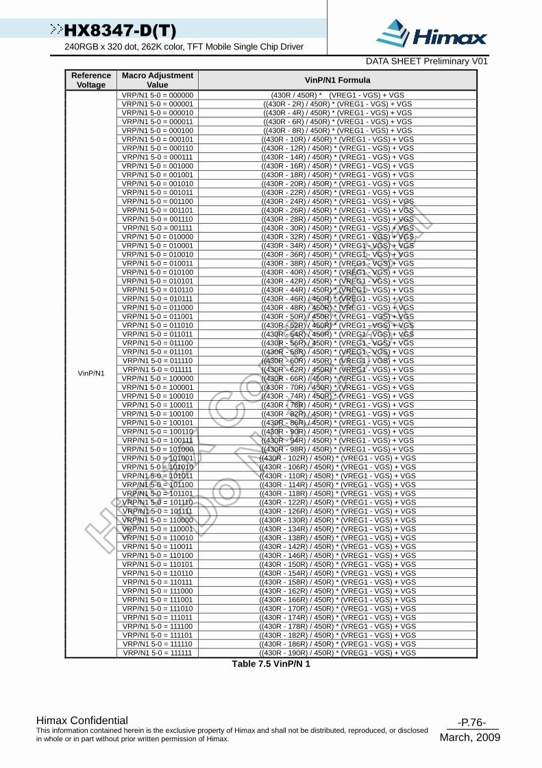
-P.76- Himax Confidential
March, 2009
This information contained herein is the exclusive property of Himax and shall not be distributed, reproduced, or disclosed in whole or in part without prior written permission of Himax.
HX8347-D(T) 240RGB x 320 dot, 262K color, TFT Mobile Single Chip Driver DATA SHEET Preliminary V01
Reference Voltage
Macro Adjustment Value VinP/N1 Formula
VRP/N1 5-0 = 000000 (430R / 450R) * (VREG1 - VGS) + VGS VRP/N1 5-0 = 000001 ((430R - 2R) / 450R) * (VREG1 - VGS) + VGS VRP/N1 5-0 = 000010 ((430R - 4R) / 450R) * (VREG1 - VGS) + VGS VRP/N1 5-0 = 000011 ((430R - 6R) / 450R) * (VREG1 - VGS) + VGS VRP/N1 5-0 = 000100 ((430R - 8R) / 450R) * (VREG1 - VGS) + VGS VRP/N1 5-0 = 000101 ((430R - 10R) / 450R) * (VREG1 - VGS) + VGS VRP/N1 5-0 = 000110 ((430R - 12R) / 450R) * (VREG1 - VGS) + VGS VRP/N1 5-0 = 000111 ((430R - 14R) / 450R) * (VREG1 - VGS) + VGS VRP/N1 5-0 = 001000 ((430R - 16R) / 450R) * (VREG1 - VGS) + VGS VRP/N1 5-0 = 001001 ((430R - 18R) / 450R) * (VREG1 - VGS) + VGS VRP/N1 5-0 = 001010 ((430R - 20R) / 450R) * (VREG1 - VGS) + VGS VRP/N1 5-0 = 001011 ((430R - 22R) / 450R) * (VREG1 - VGS) + VGS VRP/N1 5-0 = 001100 ((430R - 24R) / 450R) * (VREG1 - VGS) + VGS VRP/N1 5-0 = 001101 ((430R - 26R) / 450R) * (VREG1 - VGS) + VGS VRP/N1 5-0 = 001110 ((430R - 28R) / 450R) * (VREG1 - VGS) + VGS VRP/N1 5-0 = 001111 ((430R - 30R) / 450R) * (VREG1 - VGS) + VGS VRP/N1 5-0 = 010000 ((430R - 32R) / 450R) * (VREG1 - VGS) + VGS VRP/N1 5-0 = 010001 ((430R - 34R) / 450R) * (VREG1 - VGS) + VGS VRP/N1 5-0 = 010010 ((430R - 36R) / 450R) * (VREG1 - VGS) + VGS VRP/N1 5-0 = 010011 ((430R - 38R) / 450R) * (VREG1 - VGS) + VGS VRP/N1 5-0 = 010100 ((430R - 40R) / 450R) * (VREG1 - VGS) + VGS VRP/N1 5-0 = 010101 ((430R - 42R) / 450R) * (VREG1 - VGS) + VGS VRP/N1 5-0 = 010110 ((430R - 44R) / 450R) * (VREG1 - VGS) + VGS VRP/N1 5-0 = 010111 ((430R - 46R) / 450R) * (VREG1 - VGS) + VGS VRP/N1 5-0 = 011000 ((430R - 48R) / 450R) * (VREG1 - VGS) + VGS VRP/N1 5-0 = 011001 ((430R - 50R) / 450R) * (VREG1 - VGS) + VGS VRP/N1 5-0 = 011010 ((430R - 52R) / 450R) * (VREG1 - VGS) + VGS VRP/N1 5-0 = 011011 ((430R - 54R) / 450R) * (VREG1 - VGS) + VGS VRP/N1 5-0 = 011100 ((430R - 56R) / 450R) * (VREG1 - VGS) + VGS VRP/N1 5-0 = 011101 ((430R - 58R) / 450R) * (VREG1 - VGS) + VGS VRP/N1 5-0 = 011110 ((430R - 60R) / 450R) * (VREG1 - VGS) + VGS VRP/N1 5-0 = 011111 ((430R - 62R) / 450R) * (VREG1 - VGS) + VGS VRP/N1 5-0 = 100000 ((430R - 66R) / 450R) * (VREG1 - VGS) + VGS VRP/N1 5-0 = 100001 ((430R - 70R) / 450R) * (VREG1 - VGS) + VGS VRP/N1 5-0 = 100010 ((430R - 74R) / 450R) * (VREG1 - VGS) + VGS VRP/N1 5-0 = 100011 ((430R - 78R) / 450R) * (VREG1 - VGS) + VGS VRP/N1 5-0 = 100100 ((430R - 82R) / 450R) * (VREG1 - VGS) + VGS VRP/N1 5-0 = 100101 ((430R - 86R) / 450R) * (VREG1 - VGS) + VGS VRP/N1 5-0 = 100110 ((430R - 90R) / 450R) * (VREG1 - VGS) + VGS VRP/N1 5-0 = 100111 ((430R - 94R) / 450R) * (VREG1 - VGS) + VGS VRP/N1 5-0 = 101000 ((430R - 98R) / 450R) * (VREG1 - VGS) + VGS VRP/N1 5-0 = 101001 ((430R - 102R) / 450R) * (VREG1 - VGS) + VGS VRP/N1 5-0 = 101010 ((430R - 106R) / 450R) * (VREG1 - VGS) + VGS VRP/N1 5-0 = 101011 ((430R - 110R) / 450R) * (VREG1 - VGS) + VGS VRP/N1 5-0 = 101100 ((430R - 114R) / 450R) * (VREG1 - VGS) + VGS VRP/N1 5-0 = 101101 ((430R - 118R) / 450R) * (VREG1 - VGS) + VGS VRP/N1 5-0 = 101110 ((430R - 122R) / 450R) * (VREG1 - VGS) + VGS VRP/N1 5-0 = 101111 ((430R - 126R) / 450R) * (VREG1 - VGS) + VGS VRP/N1 5-0 = 110000 ((430R - 130R) / 450R) * (VREG1 - VGS) + VGS VRP/N1 5-0 = 110001 ((430R - 134R) / 450R) * (VREG1 - VGS) + VGS VRP/N1 5-0 = 110010 ((430R - 138R) / 450R) * (VREG1 - VGS) + VGS VRP/N1 5-0 = 110011 ((430R - 142R) / 450R) * (VREG1 - VGS) + VGS VRP/N1 5-0 = 110100 ((430R - 146R) / 450R) * (VREG1 - VGS) + VGS VRP/N1 5-0 = 110101 ((430R - 150R) / 450R) * (VREG1 - VGS) + VGS VRP/N1 5-0 = 110110 ((430R - 154R) / 450R) * (VREG1 - VGS) + VGS VRP/N1 5-0 = 110111 ((430R - 158R) / 450R) * (VREG1 - VGS) + VGS VRP/N1 5-0 = 111000 ((430R - 162R) / 450R) * (VREG1 - VGS) + VGS VRP/N1 5-0 = 111001 ((430R - 166R) / 450R) * (VREG1 - VGS) + VGS VRP/N1 5-0 = 111010 ((430R - 170R) / 450R) * (VREG1 - VGS) + VGS VRP/N1 5-0 = 111011 ((430R - 174R) / 450R) * (VREG1 - VGS) + VGS VRP/N1 5-0 = 111100 ((430R - 178R) / 450R) * (VREG1 - VGS) + VGS VRP/N1 5-0 = 111101 ((430R - 182R) / 450R) * (VREG1 - VGS) + VGS VRP/N1 5-0 = 111110 ((430R - 186R) / 450R) * (VREG1 - VGS) + VGS
VinP/N1
VRP/N1 5-0 = 111111 ((430R - 190R) / 450R) * (VREG1 - VGS) + VGS
Table 7.5 VinP/N 1

-P.77- Himax Confidential
March, 2009
This information contained herein is the exclusive property of Himax and shall not be distributed, reproduced, or disclosed in whole or in part without prior written permission of Himax.
HX8347-D(T) 240RGB x 320 dot, 262K color, TFT Mobile Single Chip Driver DATA SHEET Preliminary V01
Reference
Voltage Macro Adjustment
Value VinP/N2 Formula
VRP/N2 5-0 = 000000 (410R / 450R) * (VREG1 - VGS) + VGS VRP/N2 5-0 = 000001 ((410R - 2R) / 450R) * (VREG1 - VGS) + VGS VRP/N2 5-0 = 000010 ((410R - 4R) / 450R) * (VREG1 - VGS) + VGS VRP/N2 5-0 = 000011 ((410R - 6R) / 450R) * (VREG1 - VGS) + VGS VRP/N2 5-0 = 000100 ((410R - 8R) / 450R) * (VREG1 - VGS) + VGS VRP/N2 5-0 = 000101 ((410R - 10R) / 450R) * (VREG1 - VGS) + VGS VRP/N2 5-0 = 000110 ((410R - 12R) / 450R) * (VREG1 - VGS) + VGS VRP/N2 5-0 = 000111 ((410R - 14R) / 450R) * (VREG1 - VGS) + VGS VRP/N2 5-0 = 001000 ((410R - 16R) / 450R) * (VREG1 - VGS) + VGS VRP/N2 5-0 = 001001 ((410R - 18R) / 450R) * (VREG1 - VGS) + VGS VRP/N2 5-0 = 001010 ((410R - 20R) / 450R) * (VREG1 - VGS) + VGS VRP/N2 5-0 = 001011 ((410R - 22R) / 450R) * (VREG1 - VGS) + VGS VRP/N2 5-0 = 001100 ((410R - 24R) / 450R) * (VREG1 - VGS) + VGS VRP/N2 5-0 = 001101 ((410R - 26R) / 450R) * (VREG1 - VGS) + VGS VRP/N2 5-0 = 001110 ((410R - 28R) / 450R) * (VREG1 - VGS) + VGS VRP/N2 5-0 = 001111 ((410R - 30R) / 450R) * (VREG1 - VGS) + VGS VRP/N2 5-0 = 010000 ((410R - 32R) / 450R) * (VREG1 - VGS) + VGS VRP/N2 5-0 = 010001 ((410R - 34R) / 450R) * (VREG1 - VGS) + VGS VRP/N2 5-0 = 010010 ((410R - 36R) / 450R) * (VREG1 - VGS) + VGS VRP/N2 5-0 = 010011 ((410R - 38R) / 450R) * (VREG1 - VGS) + VGS VRP/N2 5-0 = 010100 ((410R - 40R) / 450R) * (VREG1 - VGS) + VGS VRP/N2 5-0 = 010101 ((410R - 42R) / 450R) * (VREG1 - VGS) + VGS VRP/N2 5-0 = 010110 ((410R - 44R) / 450R) * (VREG1 - VGS) + VGS VRP/N2 5-0 = 010111 ((410R - 46R) / 450R) * (VREG1 - VGS) + VGS VRP/N2 5-0 = 011000 ((410R - 48R) / 450R) * (VREG1 - VGS) + VGS VRP/N2 5-0 = 011001 ((410R - 50R) / 450R) * (VREG1 - VGS) + VGS VRP/N2 5-0 = 011010 ((410R - 52R) / 450R) * (VREG1 - VGS) + VGS VRP/N2 5-0 = 011011 ((410R - 54R) / 450R) * (VREG1 - VGS) + VGS VRP/N2 5-0 = 011100 ((410R - 56R) / 450R) * (VREG1 - VGS) + VGS VRP/N2 5-0 = 011101 ((410R - 58R) / 450R) * (VREG1 - VGS) + VGS VRP/N2 5-0 = 011110 ((410R - 60R) / 450R) * (VREG1 - VGS) + VGS VRP/N2 5-0 = 011111 ((410R - 62R) / 450R) * (VREG1 - VGS) + VGS VRP/N2 5-0 = 100000 ((410R - 66R) / 450R) * (VREG1 - VGS) + VGS VRP/N2 5-0 = 100001 ((410R - 70R) / 450R) * (VREG1 - VGS) + VGS VRP/N2 5-0 = 100010 ((410R - 74R) / 450R) * (VREG1 - VGS) + VGS VRP/N2 5-0 = 100011 ((410R - 78R) / 450R) * (VREG1 - VGS) + VGS VRP/N2 5-0 = 100100 ((410R - 82R) / 450R) * (VREG1 - VGS) + VGS VRP/N2 5-0 = 100101 ((410R - 86R) / 450R) * (VREG1 - VGS) + VGS VRP/N2 5-0 = 100110 ((410R - 90R) / 450R) * (VREG1 - VGS) + VGS VRP/N2 5-0 = 100111 ((410R - 94R) / 450R) * (VREG1 - VGS) + VGS VRP/N2 5-0 = 101000 ((410R - 98R) / 450R) * (VREG1 - VGS) + VGS VRP/N2 5-0 = 101001 ((410R - 102R) / 450R) * (VREG1 - VGS) + VGS VRP/N2 5-0 = 101010 ((410R - 106R) / 450R) * (VREG1 - VGS) + VGS VRP/N2 5-0 = 101011 ((410R - 110R) / 450R) * (VREG1 - VGS) + VGS VRP/N2 5-0 = 101100 ((410R - 114R) / 450R) * (VREG1 - VGS) + VGS VRP/N2 5-0 = 101101 ((410R - 118R) / 450R) * (VREG1 - VGS) + VGS VRP/N2 5-0 = 101110 ((410R - 122R) / 450R) * (VREG1 - VGS) + VGS VRP/N2 5-0 = 101111 ((410R - 126R) / 450R) * (VREG1 - VGS) + VGS VRP/N2 5-0 = 110000 ((410R - 130R) / 450R) * (VREG1 - VGS) + VGS VRP/N2 5-0 = 110001 ((410R - 134R) / 450R) * (VREG1 - VGS) + VGS VRP/N2 5-0 = 110010 ((410R - 138R) / 450R) * (VREG1 - VGS) + VGS VRP/N2 5-0 = 110011 ((410R - 142R) / 450R) * (VREG1 - VGS) + VGS VRP/N2 5-0 = 110100 ((410R - 146R) / 450R) * (VREG1 - VGS) + VGS VRP/N2 5-0 = 110101 ((410R - 150R) / 450R) * (VREG1 - VGS) + VGS VRP/N2 5-0 = 110110 ((410R - 154R) / 450R) * (VREG1 - VGS) + VGS VRP/N2 5-0 = 110111 ((410R - 158R) / 450R) * (VREG1 - VGS) + VGS VRP/N2 5-0 = 111000 ((410R - 162R) / 450R) * (VREG1 - VGS) + VGS VRP/N2 5-0 = 111001 ((410R - 166R) / 450R) * (VREG1 - VGS) + VGS VRP/N2 5-0 = 111010 ((410R - 170R) / 450R) * (VREG1 - VGS) + VGS VRP/N2 5-0 = 111011 ((410R - 174R) / 450R) * (VREG1 - VGS) + VGS VRP/N2 5-0 = 111100 ((410R - 178R) / 450R) * (VREG1 - VGS) + VGS VRP/N2 5-0 = 111101 ((410R - 182R) / 450R) * (VREG1 - VGS) + VGS VRP/N2 5-0 = 111110 ((410R - 186R) / 450R) * (VREG1 - VGS) + VGS
VinP/N2
VRP/N2 5-0 = 111111 ((410R - 190R) / 450R) * (VREG1 - VGS) + VGS
Table 7.6 VinP/N 2

-P.78- Himax Confidential
March, 2009
This information contained herein is the exclusive property of Himax and shall not be distributed, reproduced, or disclosed in whole or in part without prior written permission of Himax.
HX8347-D(T) 240RGB x 320 dot, 262K color, TFT Mobile Single Chip Driver DATA SHEET Preliminary V01
Reference Voltage
Macro Adjustment Value VinP/N10 Formula
VRP/N3 5-0 = 000000 (230R / 450R) * (VREG1 - VGS) + VGS VRP/N3 5-0 = 000001 ((230R - 4R) / 450R) * (VREG1 - VGS) + VGS VRP/N3 5-0 = 000010 ((230R - 8R) / 450R) * (VREG1 - VGS) + VGS VRP/N3 5-0 = 000011 ((230R - 12R) / 450R) * (VREG1 - VGS) + VGS VRP/N3 5-0 = 000100 ((230R - 16R) / 450R) * (VREG1 - VGS) + VGS VRP/N3 5-0 = 000101 ((230R - 20R) / 450R) * (VREG1 - VGS) + VGS VRP/N3 5-0 = 000110 ((230R - 24R) / 450R) * (VREG1 - VGS) + VGS VRP/N3 5-0 = 000111 ((230R - 28R) / 450R) * (VREG1 - VGS) + VGS VRP/N3 5-0 = 001000 ((230R - 32R) / 450R) * (VREG1 - VGS) + VGS VRP/N3 5-0 = 001001 ((230R - 36R) / 450R) * (VREG1 - VGS) + VGS VRP/N3 5-0 = 001010 ((230R - 40R) / 450R) * (VREG1 - VGS) + VGS VRP/N3 5-0 = 001011 ((230R - 44R) / 450R) * (VREG1 - VGS) + VGS VRP/N3 5-0 = 001100 ((230R - 48R) / 450R) * (VREG1 - VGS) + VGS VRP/N3 5-0 = 001101 ((230R - 52R) / 450R) * (VREG1 - VGS) + VGS VRP/N3 5-0 = 001110 ((230R - 56R) / 450R) * (VREG1 - VGS) + VGS VRP/N3 5-0 = 001111 ((230R - 60R) / 450R) * (VREG1 - VGS) + VGS VRP/N3 5-0 = 010000 ((230R - 64R) / 450R) * (VREG1 - VGS) + VGS VRP/N3 5-0 = 010001 ((230R - 68R) / 450R) * (VREG1 - VGS) + VGS VRP/N3 5-0 = 010010 ((230R - 72R) / 450R) * (VREG1 - VGS) + VGS VRP/N3 5-0 = 010011 ((230R - 76R) / 450R) * (VREG1 - VGS) + VGS VRP/N3 5-0 = 010100 ((230R - 80R) / 450R) * (VREG1 - VGS) + VGS VRP/N3 5-0 = 010101 ((230R - 84R) / 450R) * (VREG1 - VGS) + VGS VRP/N3 5-0 = 010110 ((230R - 88R) / 450R) * (VREG1 - VGS) + VGS VRP/N3 5-0 = 010111 ((230R - 92R) / 450R) * (VREG1 - VGS) + VGS VRP/N3 5-0 = 011000 ((230R - 96R) / 450R) * (VREG1 - VGS) + VGS VRP/N3 5-0 = 011001 ((230R - 100R) / 450R) * (VREG1 - VGS) + VGS VRP/N3 5-0 = 011010 ((230R - 104R) / 450R) * (VREG1 - VGS) + VGS VRP/N3 5-0 = 011011 ((230R - 108R) / 450R) * (VREG1 - VGS) + VGS VRP/N3 5-0 = 011100 ((230R - 112R) / 450R) * (VREG1 - VGS) + VGS VRP/N3 5-0 = 011101 ((230R - 116R) / 450R) * (VREG1 - VGS) + VGS VRP/N3 5-0 = 011110 ((230R - 120R) / 450R) * (VREG1 - VGS) + VGS VRP/N3 5-0 = 011111 ((230R - 124R) / 450R) * (VREG1 - VGS) + VGS VRP/N3 5-0 = 100000 ((230R - 128R) / 450R) * (VREG1 - VGS) + VGS VRP/N3 5-0 = 100001 ((230R - 130R) / 450R) * (VREG1 - VGS) + VGS VRP/N3 5-0 = 100010 ((230R - 132R) / 450R) * (VREG1 - VGS) + VGS VRP/N3 5-0 = 100011 ((230R - 134R) / 450R) * (VREG1 - VGS) + VGS VRP/N3 5-0 = 100100 ((230R - 136R) / 450R) * (VREG1 - VGS) + VGS VRP/N3 5-0 = 100101 ((230R - 138R) / 450R) * (VREG1 - VGS) + VGS VRP/N3 5-0 = 100110 ((230R - 140R) / 450R) * (VREG1 - VGS) + VGS VRP/N3 5-0 = 100111 ((230R - 142R) / 450R) * (VREG1 - VGS) + VGS VRP/N3 5-0 = 101000 ((230R - 144R) / 450R) * (VREG1 - VGS) + VGS VRP/N3 5-0 = 101001 ((230R - 146R) / 450R) * (VREG1 - VGS) + VGS VRP/N3 5-0 = 101010 ((230R - 148R) / 450R) * (VREG1 - VGS) + VGS VRP/N3 5-0 = 101011 ((230R - 150R) / 450R) * (VREG1 - VGS) + VGS VRP/N3 5-0 = 101100 ((230R - 152R) / 450R) * (VREG1 - VGS) + VGS VRP/N3 5-0 = 101101 ((230R - 154R) / 450R) * (VREG1 - VGS) + VGS VRP/N3 5-0 = 101110 ((230R - 156R) / 450R) * (VREG1 - VGS) + VGS VRP/N3 5-0 = 101111 ((230R - 158R) / 450R) * (VREG1 - VGS) + VGS VRP/N3 5-0 = 110000 ((230R - 160R) / 450R) * (VREG1 - VGS) + VGS VRP/N3 5-0 = 110001 ((230R - 162R) / 450R) * (VREG1 - VGS) + VGS VRP/N3 5-0 = 110010 ((230R - 164R) / 450R) * (VREG1 - VGS) + VGS VRP/N3 5-0 = 110011 ((230R - 166R) / 450R) * (VREG1 - VGS) + VGS VRP/N3 5-0 = 110100 ((230R - 168R) / 450R) * (VREG1 - VGS) + VGS VRP/N3 5-0 = 110101 ((230R - 170R) / 450R) * (VREG1 - VGS) + VGS VRP/N3 5-0 = 110110 ((230R - 172R) / 450R) * (VREG1 - VGS) + VGS VRP/N3 5-0 = 110111 ((230R - 174R) / 450R) * (VREG1 - VGS) + VGS VRP/N3 5-0 = 111000 ((230R - 176R) / 450R) * (VREG1 - VGS) + VGS VRP/N3 5-0 = 111001 ((230R - 178R) / 450R) * (VREG1 - VGS) + VGS VRP/N3 5-0 = 111010 ((230R - 180R) / 450R) * (VREG1 - VGS) + VGS VRP/N3 5-0 = 111011 ((230R - 182R) / 450R) * (VREG1 - VGS) + VGS VRP/N3 5-0 = 111100 ((230R - 184R) / 450R) * (VREG1 - VGS) + VGS VRP/N3 5-0 = 111101 ((230R - 186R) / 450R) * (VREG1 - VGS) + VGS VRP/N3 5-0 = 111110 ((230R - 188R) / 450R) * (VREG1 - VGS) + VGS
VinP/N10
VRP/N3 5-0 = 111111 ((230R - 190R) / 450R) * (VREG1 - VGS) + VGS
Table 7.7 VinP/N 10
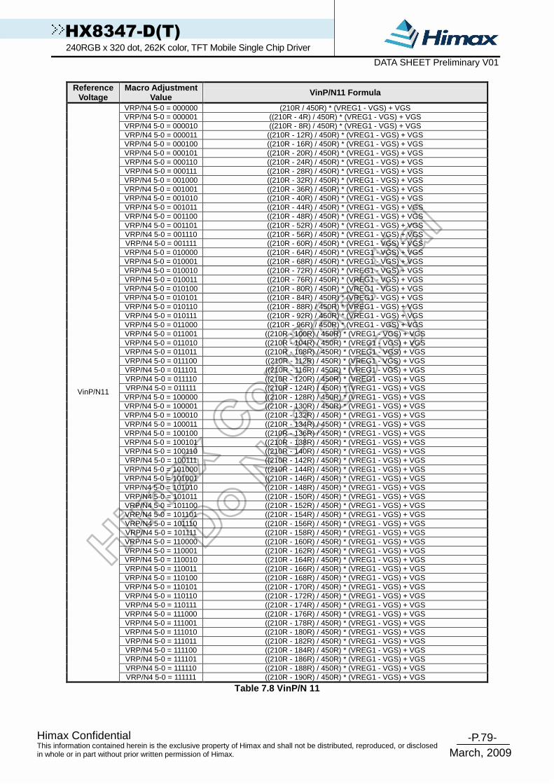
-P.79- Himax Confidential
March, 2009
This information contained herein is the exclusive property of Himax and shall not be distributed, reproduced, or disclosed in whole or in part without prior written permission of Himax.
HX8347-D(T) 240RGB x 320 dot, 262K color, TFT Mobile Single Chip Driver DATA SHEET Preliminary V01
Reference
Voltage Macro Adjustment
Value VinP/N11 Formula
VRP/N4 5-0 = 000000 (210R / 450R) * (VREG1 - VGS) + VGS VRP/N4 5-0 = 000001 ((210R - 4R) / 450R) * (VREG1 - VGS) + VGS VRP/N4 5-0 = 000010 ((210R - 8R) / 450R) * (VREG1 - VGS) + VGS VRP/N4 5-0 = 000011 ((210R - 12R) / 450R) * (VREG1 - VGS) + VGS VRP/N4 5-0 = 000100 ((210R - 16R) / 450R) * (VREG1 - VGS) + VGS VRP/N4 5-0 = 000101 ((210R - 20R) / 450R) * (VREG1 - VGS) + VGS VRP/N4 5-0 = 000110 ((210R - 24R) / 450R) * (VREG1 - VGS) + VGS VRP/N4 5-0 = 000111 ((210R - 28R) / 450R) * (VREG1 - VGS) + VGS VRP/N4 5-0 = 001000 ((210R - 32R) / 450R) * (VREG1 - VGS) + VGS VRP/N4 5-0 = 001001 ((210R - 36R) / 450R) * (VREG1 - VGS) + VGS VRP/N4 5-0 = 001010 ((210R - 40R) / 450R) * (VREG1 - VGS) + VGS VRP/N4 5-0 = 001011 ((210R - 44R) / 450R) * (VREG1 - VGS) + VGS VRP/N4 5-0 = 001100 ((210R - 48R) / 450R) * (VREG1 - VGS) + VGS VRP/N4 5-0 = 001101 ((210R - 52R) / 450R) * (VREG1 - VGS) + VGS VRP/N4 5-0 = 001110 ((210R - 56R) / 450R) * (VREG1 - VGS) + VGS VRP/N4 5-0 = 001111 ((210R - 60R) / 450R) * (VREG1 - VGS) + VGS VRP/N4 5-0 = 010000 ((210R - 64R) / 450R) * (VREG1 - VGS) + VGS VRP/N4 5-0 = 010001 ((210R - 68R) / 450R) * (VREG1 - VGS) + VGS VRP/N4 5-0 = 010010 ((210R - 72R) / 450R) * (VREG1 - VGS) + VGS VRP/N4 5-0 = 010011 ((210R - 76R) / 450R) * (VREG1 - VGS) + VGS VRP/N4 5-0 = 010100 ((210R - 80R) / 450R) * (VREG1 - VGS) + VGS VRP/N4 5-0 = 010101 ((210R - 84R) / 450R) * (VREG1 - VGS) + VGS VRP/N4 5-0 = 010110 ((210R - 88R) / 450R) * (VREG1 - VGS) + VGS VRP/N4 5-0 = 010111 ((210R - 92R) / 450R) * (VREG1 - VGS) + VGS VRP/N4 5-0 = 011000 ((210R - 96R) / 450R) * (VREG1 - VGS) + VGS VRP/N4 5-0 = 011001 ((210R - 100R) / 450R) * (VREG1 - VGS) + VGS VRP/N4 5-0 = 011010 ((210R - 104R) / 450R) * (VREG1 - VGS) + VGS VRP/N4 5-0 = 011011 ((210R - 108R) / 450R) * (VREG1 - VGS) + VGS VRP/N4 5-0 = 011100 ((210R - 112R) / 450R) * (VREG1 - VGS) + VGS VRP/N4 5-0 = 011101 ((210R - 116R) / 450R) * (VREG1 - VGS) + VGS VRP/N4 5-0 = 011110 ((210R - 120R) / 450R) * (VREG1 - VGS) + VGS VRP/N4 5-0 = 011111 ((210R - 124R) / 450R) * (VREG1 - VGS) + VGS VRP/N4 5-0 = 100000 ((210R - 128R) / 450R) * (VREG1 - VGS) + VGS VRP/N4 5-0 = 100001 ((210R - 130R) / 450R) * (VREG1 - VGS) + VGS VRP/N4 5-0 = 100010 ((210R - 132R) / 450R) * (VREG1 - VGS) + VGS VRP/N4 5-0 = 100011 ((210R - 134R) / 450R) * (VREG1 - VGS) + VGS VRP/N4 5-0 = 100100 ((210R - 136R) / 450R) * (VREG1 - VGS) + VGS VRP/N4 5-0 = 100101 ((210R - 138R) / 450R) * (VREG1 - VGS) + VGS VRP/N4 5-0 = 100110 ((210R - 140R) / 450R) * (VREG1 - VGS) + VGS VRP/N4 5-0 = 100111 ((210R - 142R) / 450R) * (VREG1 - VGS) + VGS VRP/N4 5-0 = 101000 ((210R - 144R) / 450R) * (VREG1 - VGS) + VGS VRP/N4 5-0 = 101001 ((210R - 146R) / 450R) * (VREG1 - VGS) + VGS VRP/N4 5-0 = 101010 ((210R - 148R) / 450R) * (VREG1 - VGS) + VGS VRP/N4 5-0 = 101011 ((210R - 150R) / 450R) * (VREG1 - VGS) + VGS VRP/N4 5-0 = 101100 ((210R - 152R) / 450R) * (VREG1 - VGS) + VGS VRP/N4 5-0 = 101101 ((210R - 154R) / 450R) * (VREG1 - VGS) + VGS VRP/N4 5-0 = 101110 ((210R - 156R) / 450R) * (VREG1 - VGS) + VGS VRP/N4 5-0 = 101111 ((210R - 158R) / 450R) * (VREG1 - VGS) + VGS VRP/N4 5-0 = 110000 ((210R - 160R) / 450R) * (VREG1 - VGS) + VGS VRP/N4 5-0 = 110001 ((210R - 162R) / 450R) * (VREG1 - VGS) + VGS VRP/N4 5-0 = 110010 ((210R - 164R) / 450R) * (VREG1 - VGS) + VGS VRP/N4 5-0 = 110011 ((210R - 166R) / 450R) * (VREG1 - VGS) + VGS VRP/N4 5-0 = 110100 ((210R - 168R) / 450R) * (VREG1 - VGS) + VGS VRP/N4 5-0 = 110101 ((210R - 170R) / 450R) * (VREG1 - VGS) + VGS VRP/N4 5-0 = 110110 ((210R - 172R) / 450R) * (VREG1 - VGS) + VGS VRP/N4 5-0 = 110111 ((210R - 174R) / 450R) * (VREG1 - VGS) + VGS VRP/N4 5-0 = 111000 ((210R - 176R) / 450R) * (VREG1 - VGS) + VGS VRP/N4 5-0 = 111001 ((210R - 178R) / 450R) * (VREG1 - VGS) + VGS VRP/N4 5-0 = 111010 ((210R - 180R) / 450R) * (VREG1 - VGS) + VGS VRP/N4 5-0 = 111011 ((210R - 182R) / 450R) * (VREG1 - VGS) + VGS VRP/N4 5-0 = 111100 ((210R - 184R) / 450R) * (VREG1 - VGS) + VGS VRP/N4 5-0 = 111101 ((210R - 186R) / 450R) * (VREG1 - VGS) + VGS VRP/N4 5-0 = 111110 ((210R - 188R) / 450R) * (VREG1 - VGS) + VGS
VinP/N11
VRP/N4 5-0 = 111111 ((210R - 190R) / 450R) * (VREG1 - VGS) + VGS
Table 7.8 VinP/N 11

-P.80- Himax Confidential
March, 2009
This information contained herein is the exclusive property of Himax and shall not be distributed, reproduced, or disclosed in whole or in part without prior written permission of Himax.
HX8347-D(T) 240RGB x 320 dot, 262K color, TFT Mobile Single Chip Driver DATA SHEET Preliminary V01
Reference
Voltage Macro Adjustment
Value VinP/N12 Formula
VRP/N5 5-0 = 000000 (210R / 450R) * (VREG1 - VGS) + VGS VRP/N5 5-0 = 000001 ((208R - 4R) / 450R) * (VREG1 - VGS) + VGS VRP/N5 5-0 = 000010 ((208R - 8R) / 450R) * (VREG1 - VGS) + VGS VRP/N5 5-0 = 000011 ((208R - 12R) / 450R) * (VREG1 - VGS) + VGS VRP/N5 5-0 = 000100 ((208R - 16R) / 450R) * (VREG1 - VGS) + VGS VRP/N5 5-0 = 000101 ((208R - 20R) / 450R) * (VREG1 - VGS) + VGS VRP/N5 5-0 = 000110 ((208R - 24R) / 450R) * (VREG1 - VGS) + VGS VRP/N5 5-0 = 000111 ((208R - 28R) / 450R) * (VREG1 - VGS) + VGS VRP/N5 5-0 = 001000 ((208R - 32R) / 450R) * (VREG1 - VGS) + VGS VRP/N5 5-0 = 001001 ((208R - 36R) / 450R) * (VREG1 - VGS) + VGS VRP/N5 5-0 = 001010 ((208R - 40R) / 450R) * (VREG1 - VGS) + VGS VRP/N5 5-0 = 001011 ((208R - 44R) / 450R) * (VREG1 - VGS) + VGS VRP/N5 5-0 = 001100 ((208R - 48R) / 450R) * (VREG1 - VGS) + VGS VRP/N5 5-0 = 001101 ((208R - 52R) / 450R) * (VREG1 - VGS) + VGS VRP/N5 5-0 = 001110 ((208R - 56R) / 450R) * (VREG1 - VGS) + VGS VRP/N5 5-0 = 001111 ((208R - 60R) / 450R) * (VREG1 - VGS) + VGS VRP/N5 5-0 = 010000 ((208R - 64R) / 450R) * (VREG1 - VGS) + VGS VRP/N5 5-0 = 010001 ((208R - 68R) / 450R) * (VREG1 - VGS) + VGS VRP/N5 5-0 = 010010 ((208R - 72R) / 450R) * (VREG1 - VGS) + VGS VRP/N5 5-0 = 010011 ((208R - 76R) / 450R) * (VREG1 - VGS) + VGS VRP/N5 5-0 = 010100 ((208R - 80R) / 450R) * (VREG1 - VGS) + VGS VRP/N5 5-0 = 010101 ((208R - 84R) / 450R) * (VREG1 - VGS) + VGS VRP/N5 5-0 = 010110 ((208R - 88R) / 450R) * (VREG1 - VGS) + VGS VRP/N5 5-0 = 010111 ((208R - 92R) / 450R) * (VREG1 - VGS) + VGS VRP/N5 5-0 = 011000 ((208R - 96R) / 450R) * (VREG1 - VGS) + VGS VRP/N5 5-0 = 011001 ((208R - 100R) / 450R) * (VREG1 - VGS) + VGS VRP/N5 5-0 = 011010 ((208R - 104R) / 450R) * (VREG1 - VGS) + VGS VRP/N5 5-0 = 011011 ((208R - 108R) / 450R) * (VREG1 - VGS) + VGS VRP/N5 5-0 = 011100 ((208R - 112R) / 450R) * (VREG1 - VGS) + VGS VRP/N5 5-0 = 011101 ((208R - 116R) / 450R) * (VREG1 - VGS) + VGS VRP/N5 5-0 = 011110 ((208R - 120R) / 450R) * (VREG1 - VGS) + VGS VRP/N5 5-0 = 011111 ((208R - 124R) / 450R) * (VREG1 - VGS) + VGS VRP/N5 5-0 = 100000 ((208R - 128R) / 450R) * (VREG1 - VGS) + VGS VRP/N5 5-0 = 100001 ((208R - 130R) / 450R) * (VREG1 - VGS) + VGS VRP/N5 5-0 = 100010 ((208R - 132R) / 450R) * (VREG1 - VGS) + VGS VRP/N5 5-0 = 100011 ((208R - 134R) / 450R) * (VREG1 - VGS) + VGS VRP/N5 5-0 = 100100 ((208R - 136R) / 450R) * (VREG1 - VGS) + VGS VRP/N5 5-0 = 100101 ((208R - 138R) / 450R) * (VREG1 - VGS) + VGS VRP/N5 5-0 = 100110 ((208R - 140R) / 450R) * (VREG1 - VGS) + VGS VRP/N5 5-0 = 100111 ((208R - 142R) / 450R) * (VREG1 - VGS) + VGS VRP/N5 5-0 = 101000 ((208R - 144R) / 450R) * (VREG1 - VGS) + VGS VRP/N5 5-0 = 101001 ((208R - 146R) / 450R) * (VREG1 - VGS) + VGS VRP/N5 5-0 = 101010 ((208R - 148R) / 450R) * (VREG1 - VGS) + VGS VRP/N5 5-0 = 101011 ((208R - 150R) / 450R) * (VREG1 - VGS) + VGS VRP/N5 5-0 = 101100 ((208R - 152R) / 450R) * (VREG1 - VGS) + VGS VRP/N5 5-0 = 101101 ((208R - 154R) / 450R) * (VREG1 - VGS) + VGS VRP/N5 5-0 = 101110 ((208R - 156R) / 450R) * (VREG1 - VGS) + VGS VRP/N5 5-0 = 101111 ((208R - 158R) / 450R) * (VREG1 - VGS) + VGS VRP/N5 5-0 = 110000 ((208R - 160R) / 450R) * (VREG1 - VGS) + VGS VRP/N5 5-0 = 110001 ((208R - 162R) / 450R) * (VREG1 - VGS) + VGS VRP/N5 5-0 = 110010 ((208R - 164R) / 450R) * (VREG1 - VGS) + VGS VRP/N5 5-0 = 110011 ((208R - 166R) / 450R) * (VREG1 - VGS) + VGS VRP/N5 5-0 = 110100 ((208R - 168R) / 450R) * (VREG1 - VGS) + VGS VRP/N5 5-0 = 110101 ((208R - 170R) / 450R) * (VREG1 - VGS) + VGS VRP/N5 5-0 = 110110 ((208R - 172R) / 450R) * (VREG1 - VGS) + VGS VRP/N5 5-0 = 110111 ((208R - 174R) / 450R) * (VREG1 - VGS) + VGS VRP/N5 5-0 = 111000 ((208R - 176R) / 450R) * (VREG1 - VGS) + VGS VRP/N5 5-0 = 111001 ((208R - 178R) / 450R) * (VREG1 - VGS) + VGS VRP/N5 5-0 = 111010 ((208R - 180R) / 450R) * (VREG1 - VGS) + VGS VRP/N5 5-0 = 111011 ((208R - 182R) / 450R) * (VREG1 - VGS) + VGS VRP/N5 5-0 = 111100 ((208R - 184R) / 450R) * (VREG1 - VGS) + VGS VRP/N5 5-0 = 111101 ((208R - 186R) / 450R) * (VREG1 - VGS) + VGS VRP/N5 5-0 = 111110 ((208R - 188R) / 450R) * (VREG1 - VGS) + VGS
VinP/N12
VRP/N5 5-0 = 111111 VGS
Table 7.9 VinP/N 12
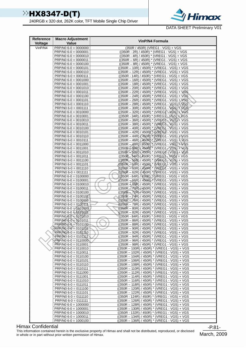
-P.81- Himax Confidential
March, 2009
This information contained herein is the exclusive property of Himax and shall not be distributed, reproduced, or disclosed in whole or in part without prior written permission of Himax.
HX8347-D(T) 240RGB x 320 dot, 262K color, TFT Mobile Single Chip Driver DATA SHEET Preliminary V01
Reference
Voltage Macro Adjustment
Value VinP/N4 Formula
PRP/N0 6-0 = 0000000 (350R / 450R) (VREG1 - VGS) + VGS PRP/N0 6-0 = 0000001 ((350R - 2R) / 450R) * (VREG1 - VGS) + VGS PRP/N0 6-0 = 0000010 ((350R - 4R) / 450R) * (VREG1 - VGS) + VGS PRP/N0 6-0 = 0000011 ((350R – 6R) / 450R) * (VREG1 - VGS) + VGS PRP/N0 6-0 = 0000100 ((350R – 8R) / 450R) * (VREG1 - VGS) + VGS PRP/N0 6-0 = 0000101 ((350R – 10R) / 450R) * (VREG1 - VGS) + VGS PRP/N0 6-0 = 0000110 ((350R – 12R) / 450R) * (VREG1 - VGS) + VGS PRP/N0 6-0 = 0000111 ((350R - 14R) / 450R) * (VREG1 - VGS) + VGS PRP/N0 6-0 = 0001000 ((350R – 16R) / 450R) * (VREG1 - VGS) + VGS PRP/N0 6-0 = 0001001 ((350R – 18R) / 450R) * (VREG1 - VGS) + VGS PRP/N0 6-0 = 0001010 ((350R – 20R) / 450R) * (VREG1 - VGS) + VGS PRP/N0 6-0 = 0001011 ((350R – 22R) / 450R) * (VREG1 - VGS) + VGS PRP/N0 6-0 = 0001100 ((350R – 24R) / 450R) * (VREG1 - VGS) + VGS PRP/N0 6-0 = 0001101 ((350R – 26R) / 450R) * (VREG1 - VGS) + VGS PRP/N0 6-0 = 0001110 ((350R – 28R) / 450R) * (VREG1 - VGS) + VGS PRP/N0 6-0 = 0001111 ((350R – 30R) / 450R) * (VREG1 - VGS) + VGS PRP/N0 6-0 = 0010000 ((350R – 32R) / 450R) * (VREG1 - VGS) + VGS PRP/N0 6-0 = 0010001 ((350R - 34R) / 450R) * (VREG1 - VGS) + VGS PRP/N0 6-0 = 0010010 ((350R – 36R) / 450R) * (VREG1 - VGS) + VGS PRP/N0 6-0 = 0010011 ((350R – 38R) / 450R) * (VREG1 - VGS) + VGS PRP/N0 6-0 = 0010100 ((350R – 40R) / 450R) * (VREG1 - VGS) + VGS PRP/N0 6-0 = 0010101 ((350R – 42R) / 450R) * (VREG1 - VGS) + VGS PRP/N0 6-0 = 0010110 ((350R – 44R) / 450R) * (VREG1 - VGS) + VGS PRP/N0 6-0 = 0010111 ((350R – 46R) / 450R) * (VREG1 - VGS) + VGS PRP/N0 6-0 = 0011000 ((350R – 48R) / 450R) * (VREG1 - VGS) + VGS PRP/N0 6-0 = 0011001 ((350R – 50R) / 450R) * (VREG1 - VGS) + VGS PRP/N0 6-0 = 0011010 ((350R – 52R) / 450R) * (VREG1 - VGS) + VGS PRP/N0 6-0 = 0011011 ((350R - 54R) / 450R) * (VREG1 - VGS) + VGS PRP/N0 6-0 = 0011100 ((350R – 56R) / 450R) * (VREG1 - VGS) + VGS PRP/N0 6-0 = 0011101 ((350R – 58R) / 450R) * (VREG1 - VGS) + VGS PRP/N0 6-0 = 0011110 ((350R – 60R) / 450R) * (VREG1 - VGS) + VGS PRP/N0 6-0 = 0011111 ((350R – 62R) / 450R) * (VREG1 - VGS) + VGS PRP/N0 6-0 = 0100000 ((350R - 64R) / 450R) * (VREG1 - VGS) + VGS PRP/N0 6-0 = 0100001 ((350R – 66R) / 450R) * (VREG1 - VGS) + VGS PRP/N0 6-0 = 0100010 ((350R – 68R) / 450R) * (VREG1 - VGS) + VGS PRP/N0 6-0 = 0100011 ((350R – 70R) / 450R) * (VREG1 - VGS) + VGS PRP/N0 6-0 = 0100100 ((350R – 72R) / 450R) * (VREG1 - VGS) + VGS PRP/N0 6-0 = 0100101 ((350R – 74R) / 450R) * (VREG1 - VGS) + VGS PRP/N0 6-0 = 0100110 ((350R – 76R) / 450R) * (VREG1 - VGS) + VGS PRP/N0 6-0 = 0100111 ((350R – 78R) / 450R) * (VREG1 - VGS) + VGS PRP/N0 6-0 = 0101000 ((350R – 80R) / 450R) * (VREG1 - VGS) + VGS PRP/N0 6-0 = 0101001 ((350R – 82R) / 450R) * (VREG1 - VGS) + VGS PRP/N0 6-0 = 0101010 ((350R - 84R) / 450R) * (VREG1 - VGS) + VGS PRP/N0 6-0 = 0101011 ((350R – 86R) / 450R) * (VREG1 - VGS) + VGS PRP/N0 6-0 = 0101100 ((350R – 88R) / 450R) * (VREG1 - VGS) + VGS PRP/N0 6-0 = 0101101 ((350R – 90R) / 450R) * (VREG1 - VGS) + VGS PRP/N0 6-0 = 0101110 ((350R – 92R) / 450R) * (VREG1 - VGS) + VGS PRP/N0 6-0 = 0101111 ((350R – 94R) / 450R) * (VREG1 - VGS) + VGS PRP/N0 6-0 = 0110000 ((350R – 96R) / 450R) * (VREG1 - VGS) + VGS PRP/N0 6-0 = 0110001 ((350R – 98R) / 450R) * (VREG1 - VGS) + VGS PRP/N0 6-0 = 0110010 ((350R – 100R) / 450R) * (VREG1 - VGS) + VGS PRP/N0 6-0 = 0110011 ((350R – 102R) / 450R) * (VREG1 - VGS) + VGS PRP/N0 6-0 = 0110100 ((350R – 104R) / 450R) * (VREG1 - VGS) + VGS PRP/N0 6-0 = 0110101 ((350R – 106R) / 450R) * (VREG1 - VGS) + VGS PRP/N0 6-0 = 0110110 ((350R – 108R) / 450R) * (VREG1 - VGS) + VGS PRP/N0 6-0 = 0110111 ((350R – 110R) / 450R) * (VREG1 - VGS) + VGS PRP/N0 6-0 = 0111000 ((350R – 112R) / 450R) * (VREG1 - VGS) + VGS PRP/N0 6-0 = 0111001 ((350R – 114R) / 450R) * (VREG1 - VGS) + VGS PRP/N0 6-0 = 0111010 ((350R – 116R) / 450R) * (VREG1 - VGS) + VGS PRP/N0 6-0 = 0111011 ((350R – 118R) / 450R) * (VREG1 - VGS) + VGS PRP/N0 6-0 = 0111100 ((350R – 120R) / 450R) * (VREG1 - VGS) + VGS PRP/N0 6-0 = 0111101 ((350R – 122R) / 450R) * (VREG1 - VGS) + VGS PRP/N0 6-0 = 0111110 ((350R - 124R) / 450R) * (VREG1 - VGS) + VGS PRP/N0 6-0 = 0111111 ((350R – 126R) / 450R) * (VREG1 - VGS) + VGS PRP/N0 6-0 = 1000000 ((350R – 128R) / 450R) * (VREG1 - VGS) + VGS PRP/N0 6-0 = 1000001 ((350R – 130R) / 450R) * (VREG1 - VGS) + VGS PRP/N0 6-0 = 1000010 ((350R - 132R) / 450R) * (VREG1 - VGS) + VGS PRP/N0 6-0 = 1000011 ((350R – 134R) / 450R) * (VREG1 - VGS) + VGS
VinP/N4
PRP/N0 6-0 = 1000100 ((350R – 136R) / 450R) * (VREG1 - VGS) + VGS

-P.82- Himax Confidential
March, 2009
This information contained herein is the exclusive property of Himax and shall not be distributed, reproduced, or disclosed in whole or in part without prior written permission of Himax.
HX8347-D(T) 240RGB x 320 dot, 262K color, TFT Mobile Single Chip Driver DATA SHEET Preliminary V01
Reference Voltage
Macro Adjustment Value VinP/N4 Formula
PRP/N0 6-0 = 1000101 ((350R – 138R) / 450R) * (VREG1 - VGS) + VGS PRP/N0 6-0 = 1000110 ((350R – 140R) / 450R) * (VREG1 - VGS) + VGS PRP/N0 6-0 = 1000111 ((350R – 142R) / 450R) * (VREG1 - VGS) + VGS PRP/N0 6-0 = 1001000 ((350R – 144R) / 450R) * (VREG1 - VGS) + VGS PRP/N0 6-0 = 1001001 ((350R – 146R) / 450R) * (VREG1 - VGS) + VGS PRP/N0 6-0 = 1001010 ((350R – 148R) / 450R) * (VREG1 - VGS) + VGS PRP/N0 6-0 = 1001011 ((350R – 150R) / 450R) * (VREG1 - VGS) + VGS PRP/N0 6-0 = 1001100 ((350R - 152R) / 450R) * (VREG1 - VGS) + VGS PRP/N0 6-0 = 1001101 ((350R – 154R) / 450R) * (VREG1 - VGS) + VGS PRP/N0 6-0 = 1001110 ((350R – 156R) / 450R) * (VREG1 - VGS) + VGS PRP/N0 6-0 = 1001111 ((350R – 158R) / 450R) * (VREG1 - VGS) + VGS PRP/N0 6-0 = 1010000 ((350R – 160R) / 450R) * (VREG1 - VGS) + VGS PRP/N0 6-0 = 1010001 ((350R – 162R) / 450R) * (VREG1 - VGS) + VGS PRP/N0 6-0 = 1010010 ((350R – 164R) / 450R) * (VREG1 - VGS) + VGS PRP/N0 6-0 = 1010011 ((350R – 166R) / 450R) * (VREG1 - VGS) + VGS PRP/N0 6-0 = 1010100 ((350R – 168R) / 450R) * (VREG1 - VGS) + VGS PRP/N0 6-0 = 1010101 ((350R – 170R) / 450R) * (VREG1 - VGS) + VGS PRP/N0 6-0 = 1010110 ((350R – 172R) / 450R) * (VREG1 - VGS) + VGS PRP/N0 6-0 = 1010111 ((350R - 174R) / 450R) * (VREG1 - VGS) + VGS PRP/N0 6-0 = 1011000 ((350R – 176R) / 450R) * (VREG1 - VGS) + VGS PRP/N0 6-0 = 1011001 ((350R – 178R) / 450R) * (VREG1 - VGS) + VGS PRP/N0 6-0 = 1011010 ((350R – 180R) / 450R) * (VREG1 - VGS) + VGS PRP/N0 6-0 = 1011011 ((350R – 182R) / 450R) * (VREG1 - VGS) + VGS PRP/N0 6-0 = 1011100 ((350R – 184R) / 450R) * (VREG1 - VGS) + VGS PRP/N0 6-0 = 1011101 ((350R – 186R) / 450R) * (VREG1 - VGS) + VGS PRP/N0 6-0 = 1011110 ((350R – 188R) / 450R) * (VREG1 - VGS) + VGS PRP/N0 6-0 = 1011111 ((350R – 190R) / 450R) * (VREG1 - VGS) + VGS PRP/N0 6-0 = 1100000 ((350R – 192R) / 450R) * (VREG1 - VGS) + VGS PRP/N0 6-0 = 1100001 ((350R – 194R) / 450R) * (VREG1 - VGS) + VGS PRP/N0 6-0 = 1100010 ((350R – 196R) / 450R) * (VREG1 - VGS) + VGS PRP/N0 6-0 = 1100011 ((350R – 198R) / 450R) * (VREG1 - VGS) + VGS PRP/N0 6-0 = 1100100 ((350R – 200R) / 450R) * (VREG1 - VGS) + VGS PRP/N0 6-0 = 1100101 ((350R – 202R) / 450R) * (VREG1 - VGS) + VGS PRP/N0 6-0 = 1100110 ((350R – 204R) / 450R) * (VREG1 - VGS) + VGS PRP/N0 6-0 = 1100111 ((350R – 206R) / 450R) * (VREG1 - VGS) + VGS PRP/N0 6-0 = 1101000 ((350R – 208R) / 450R) * (VREG1 - VGS) + VGS PRP/N0 6-0 = 1101001 ((350R – 210R) / 450R) * (VREG1 - VGS) + VGS PRP/N0 6-0 = 1101010 ((350R – 212R) / 450R) * (VREG1 - VGS) + VGS PRP/N0 6-0 = 1101011 ((350R – 214R) / 450R) * (VREG1 - VGS) + VGS PRP/N0 6-0 = 1101100 ((350R – 216R) / 450R) * (VREG1 - VGS) + VGS PRP/N0 6-0 = 1101101 ((350R – 218R) / 450R) * (VREG1 - VGS) + VGS PRP/N0 6-0 = 1101110 ((350R – 220R) / 450R) * (VREG1 - VGS) + VGS PRP/N0 6-0 = 1101111 ((350R – 223R) / 450R) * (VREG1 - VGS) + VGS PRP/N0 6-0 = 1110000 ((350R – 224R) / 450R) * (VREG1 - VGS) + VGS PRP/N0 6-0 = 1110001 ((350R – 226R) / 450R) * (VREG1 - VGS) + VGS PRP/N0 6-0 = 1110010 ((350R – 228R) / 450R) * (VREG1 - VGS) + VGS PRP/N0 6-0 = 1110011 ((350R – 230R) / 450R) * (VREG1 - VGS) + VGS PRP/N0 6-0 = 1110100 ((350R – 232R) / 450R) * (VREG1 - VGS) + VGS PRP/N0 6-0 = 1110101 ((350R – 234R) / 450R) * (VREG1 - VGS) + VGS PRP/N0 6-0 = 1110110 ((350R – 236R) / 450R) * (VREG1 - VGS) + VGS PRP/N0 6-0 = 1110111 ((350R – 238R) / 450R) * (VREG1 - VGS) + VGS PRP/N0 6-0 = 1111000 ((350R – 240R) / 450R) * (VREG1 - VGS) + VGS PRP/N0 6-0 = 1111001 ((350R – 243R) / 450R) * (VREG1 - VGS) + VGS PRP/N0 6-0 = 1111010 ((350R – 244R) / 450R) * (VREG1 - VGS) + VGS PRP/N0 6-0 = 1111011 ((350R – 246R) / 450R) * (VREG1 - VGS) + VGS PRP/N0 6-0 = 1111100 ((350R – 248R) / 450R) * (VREG1 - VGS) + VGS PRP/N0 6-0 = 1111101 ((350R – 250R) / 450R) * (VREG1 - VGS) + VGS PRP/N0 6-0 = 1111110 ((350R – 252R) / 450R) * (VREG1 - VGS) + VGS PRP/N0 6-0 = 1111111 ((350R – 254R) / 450R) * (VREG1 - VGS) + VGS
Table 7.10 VinP/N4

-P.83- Himax Confidential
March, 2009
This information contained herein is the exclusive property of Himax and shall not be distributed, reproduced, or disclosed in whole or in part without prior written permission of Himax.
HX8347-D(T) 240RGB x 320 dot, 262K color, TFT Mobile Single Chip Driver DATA SHEET Preliminary V01
Reference
Voltage Macro Adjustment
Value VinP/N8 Formula
PRP/N1 6-0 = 0000000 (354R / 450R) (VREG1 - VGS) + VGS PRP/N1 6-0 = 0000001 ((354R - 2R) / 450R) * (VREG1 - VGS) + VGS PRP/N1 6-0 = 0000010 ((354R - 4R) / 450R) * (VREG1 - VGS) + VGS PRP/N1 6-0 = 0000011 ((354R – 6R) / 450R) * (VREG1 - VGS) + VGS PRP/N1 6-0 = 0000100 ((354R – 8R) / 450R) * (VREG1 - VGS) + VGS PRP/N1 6-0 = 0000101 ((354R – 10R) / 450R) * (VREG1 - VGS) + VGS PRP/N1 6-0 = 0000110 ((354R – 12R) / 450R) * (VREG1 - VGS) + VGS PRP/N1 6-0 = 0000111 ((354R - 14R) / 450R) * (VREG1 - VGS) + VGS PRP/N1 6-0 = 0001000 ((354R – 16R) / 450R) * (VREG1 - VGS) + VGS PRP/N1 6-0 = 0001001 ((354R – 18R) / 450R) * (VREG1 - VGS) + VGS PRP/N1 6-0 = 0001010 ((354R – 20R) / 450R) * (VREG1 - VGS) + VGS PRP/N1 6-0 = 0001011 ((354R – 22R) / 450R) * (VREG1 - VGS) + VGS PRP/N1 6-0 = 0001100 ((354R – 24R) / 450R) * (VREG1 - VGS) + VGS PRP/N1 6-0 = 0001101 ((354R – 26R) / 450R) * (VREG1 - VGS) + VGS PRP/N1 6-0 = 0001110 ((354R – 28R) / 450R) * (VREG1 - VGS) + VGS PRP/N1 6-0 = 0001111 ((354R – 30R) / 450R) * (VREG1 - VGS) + VGS PRP/N1 6-0 = 0010000 ((354R – 32R) / 450R) * (VREG1 - VGS) + VGS PRP/N1 6-0 = 0010001 ((354R - 34R) / 450R) * (VREG1 - VGS) + VGS PRP/N1 6-0 = 0010010 ((354R – 36R) / 450R) * (VREG1 - VGS) + VGS PRP/N1 6-0 = 0010011 ((354R – 38R) / 450R) * (VREG1 - VGS) + VGS PRP/N1 6-0 = 0010100 ((354R – 40R) / 450R) * (VREG1 - VGS) + VGS PRP/N1 6-0 = 0010101 ((354R – 42R) / 450R) * (VREG1 - VGS) + VGS PRP/N1 6-0 = 0010110 ((354R – 44R) / 450R) * (VREG1 - VGS) + VGS PRP/N1 6-0 = 0010111 ((354R – 46R) / 450R) * (VREG1 - VGS) + VGS PRP/N1 6-0 = 0011000 ((354R – 48R) / 450R) * (VREG1 - VGS) + VGS PRP/N1 6-0 = 0011001 ((354R – 50R) / 450R) * (VREG1 - VGS) + VGS PRP/N1 6-0 = 0011010 ((354R – 52R) / 450R) * (VREG1 - VGS) + VGS PRP/N1 6-0 = 0011011 ((354R - 54R) / 450R) * (VREG1 - VGS) + VGS PRP/N1 6-0 = 0011100 ((354R – 56R) / 450R) * (VREG1 - VGS) + VGS PRP/N1 6-0 = 0011101 ((354R – 58R) / 450R) * (VREG1 - VGS) + VGS PRP/N1 6-0 = 0011110 ((354R – 60R) / 450R) * (VREG1 - VGS) + VGS PRP/N1 6-0 = 0011111 ((354R – 62R) / 450R) * (VREG1 - VGS) + VGS PRP/N1 6-0 = 0100000 ((354R - 64R) / 450R) * (VREG1 - VGS) + VGS PRP/N1 6-0 = 0100001 ((354R – 66R) / 450R) * (VREG1 - VGS) + VGS PRP/N1 6-0 = 0100010 ((354R – 68R) / 450R) * (VREG1 - VGS) + VGS PRP/N1 6-0 = 0100011 ((354R – 70R) / 450R) * (VREG1 - VGS) + VGS PRP/N1 6-0 = 0100100 ((354R – 72R) / 450R) * (VREG1 - VGS) + VGS PRP/N1 6-0 = 0100101 ((354R – 74R) / 450R) * (VREG1 - VGS) + VGS PRP/N1 6-0 = 0100110 ((354R – 76R) / 450R) * (VREG1 - VGS) + VGS PRP/N1 6-0 = 0100111 ((354R – 78R) / 450R) * (VREG1 - VGS) + VGS PRP/N1 6-0 = 0101000 ((354R – 80R) / 450R) * (VREG1 - VGS) + VGS PRP/N1 6-0 = 0101001 ((354R – 82R) / 450R) * (VREG1 - VGS) + VGS PRP/N1 6-0 = 0101010 ((354R - 84R) / 450R) * (VREG1 - VGS) + VGS PRP/N1 6-0 = 0101011 ((354R – 86R) / 450R) * (VREG1 - VGS) + VGS PRP/N1 6-0 = 0101100 ((354R – 88R) / 450R) * (VREG1 - VGS) + VGS PRP/N1 6-0 = 0101101 ((354R – 90R) / 450R) * (VREG1 - VGS) + VGS PRP/N1 6-0 = 0101110 ((354R – 92R) / 450R) * (VREG1 - VGS) + VGS PRP/N1 6-0 = 0101111 ((354R – 94R) / 450R) * (VREG1 - VGS) + VGS PRP/N1 6-0 = 0110000 ((354R – 96R) / 450R) * (VREG1 - VGS) + VGS PRP/N1 6-0 = 0110001 ((354R – 98R) / 450R) * (VREG1 - VGS) + VGS PRP/N1 6-0 = 0110010 ((354R – 100R) / 450R) * (VREG1 - VGS) + VGS PRP/N1 6-0 = 0110011 ((354R – 102R) / 450R) * (VREG1 - VGS) + VGS PRP/N1 6-0 = 0110100 ((354R – 104R) / 450R) * (VREG1 - VGS) + VGS PRP/N1 6-0 = 0110101 ((354R – 106R) / 450R) * (VREG1 - VGS) + VGS PRP/N1 6-0 = 0110110 ((354R – 108R) / 450R) * (VREG1 - VGS) + VGS PRP/N1 6-0 = 0110111 ((354R – 110R) / 450R) * (VREG1 - VGS) + VGS PRP/N1 6-0 = 0111000 ((354R – 112R) / 450R) * (VREG1 - VGS) + VGS PRP/N1 6-0 = 0111001 ((354R – 114R) / 450R) * (VREG1 - VGS) + VGS PRP/N1 6-0 = 0111010 ((354R – 116R) / 450R) * (VREG1 - VGS) + VGS PRP/N1 6-0 = 0111011 ((354R – 118R) / 450R) * (VREG1 - VGS) + VGS PRP/N1 6-0 = 0111100 ((354R – 120R) / 450R) * (VREG1 - VGS) + VGS PRP/N1 6-0 = 0111101 ((354R – 122R) / 450R) * (VREG1 - VGS) + VGS PRP/N1 6-0 = 0111110 ((354R - 124R) / 450R) * (VREG1 - VGS) + VGS PRP/N1 6-0 = 0111111 ((354R – 126R) / 450R) * (VREG1 - VGS) + VGS PRP/N1 6-0 = 1000000 ((354R – 128R) / 450R) * (VREG1 - VGS) + VGS PRP/N1 6-0 = 1000001 ((354R – 130R) / 450R) * (VREG1 - VGS) + VGS PRP/N1 6-0 = 1000010 ((354R - 132R) / 450R) * (VREG1 - VGS) + VGS PRP/N1 6-0 = 1000011 ((354R – 134R) / 450R) * (VREG1 - VGS) + VGS
VinP/N8
PRP/N1 6-0 = 1000100 ((354R – 136R) / 450R) * (VREG1 - VGS) + VGS

-P.84- Himax Confidential
March, 2009
This information contained herein is the exclusive property of Himax and shall not be distributed, reproduced, or disclosed in whole or in part without prior written permission of Himax.
HX8347-D(T) 240RGB x 320 dot, 262K color, TFT Mobile Single Chip Driver DATA SHEET Preliminary V01
Reference Voltage
Macro Adjustment Value VinP/N8 Formula
PRP/N1 6-0 = 1000101 ((354R – 138R) / 450R) * (VREG1 - VGS) + VGS PRP/N1 6-0 = 1000110 ((354R – 140R) / 450R) * (VREG1 - VGS) + VGS PRP/N1 6-0 = 1000111 ((354R – 142R) / 450R) * (VREG1 - VGS) + VGS PRP/N1 6-0 = 1001000 ((354R – 144R) / 450R) * (VREG1 - VGS) + VGS PRP/N1 6-0 = 1001001 ((354R – 146R) / 450R) * (VREG1 - VGS) + VGS PRP/N1 6-0 = 1001010 ((354R – 148R) / 450R) * (VREG1 - VGS) + VGS PRP/N1 6-0 = 1001011 ((354R – 150R) / 450R) * (VREG1 - VGS) + VGS PRP/N1 6-0 = 1001100 ((354R - 152R) / 450R) * (VREG1 - VGS) + VGS PRP/N1 6-0 = 1001101 ((354R – 154R) / 450R) * (VREG1 - VGS) + VGS PRP/N1 6-0 = 1001110 ((354R – 156R) / 450R) * (VREG1 - VGS) + VGS PRP/N1 6-0 = 1001111 ((354R – 158R) / 450R) * (VREG1 - VGS) + VGS PRP/N1 6-0 = 1010000 ((354R – 160R) / 450R) * (VREG1 - VGS) + VGS PRP/N1 6-0 = 1010001 ((354R – 162R) / 450R) * (VREG1 - VGS) + VGS PRP/N1 6-0 = 1010010 ((354R – 164R) / 450R) * (VREG1 - VGS) + VGS PRP/N1 6-0 = 1010011 ((354R – 166R) / 450R) * (VREG1 - VGS) + VGS PRP/N1 6-0 = 1010100 ((354R – 168R) / 450R) * (VREG1 - VGS) + VGS PRP/N1 6-0 = 1010101 ((354R – 170R) / 450R) * (VREG1 - VGS) + VGS PRP/N1 6-0 = 1010110 ((354R – 172R) / 450R) * (VREG1 - VGS) + VGS PRP/N1 6-0 = 1010111 ((354R - 174R) / 450R) * (VREG1 - VGS) + VGS PRP/N1 6-0 = 1011000 ((354R – 176R) / 450R) * (VREG1 - VGS) + VGS PRP/N1 6-0 = 1011001 ((354R - 178R) / 450R) * (VREG1 - VGS) + VGS PRP/N1 6-0 = 1011010 ((354R – 180R) / 450R) * (VREG1 - VGS) + VGS PRP/N1 6-0 = 1011011 ((354R – 182R) / 450R) * (VREG1 - VGS) + VGS PRP/N1 6-0 = 1011100 ((354R - 184R) / 450R) * (VREG1 - VGS) + VGS PRP/N1 6-0 = 1011101 ((354R – 186R) / 450R) * (VREG1 - VGS) + VGS PRP/N1 6-0 = 1011110 ((354R - 188R) / 450R) * (VREG1 - VGS) + VGS PRP/N1 6-0 = 1011111 ((354R – 190R) / 450R) * (VREG1 - VGS) + VGS PRP/N1 6-0 = 1100000 ((354R – 192R) / 450R) * (VREG1 - VGS) + VGS PRP/N1 6-0 = 1100001 ((354R - 194R) / 450R) * (VREG1 - VGS) + VGS PRP/N1 6-0 = 1100010 ((354R – 196R) / 450R) * (VREG1 - VGS) + VGS PRP/N1 6-0 = 1100011 ((354R - 198R) / 450R) * (VREG1 - VGS) + VGS PRP/N1 6-0 = 1100100 ((354R – 200R) / 450R) * (VREG1 - VGS) + VGS PRP/N1 6-0 = 1100101 ((354R – 202R) / 450R) * (VREG1 - VGS) + VGS PRP/N1 6-0 = 1100110 ((354R - 204R) / 450R) * (VREG1 - VGS) + VGS PRP/N1 6-0 = 1100111 ((354R – 206R) / 450R) * (VREG1 - VGS) + VGS PRP/N1 6-0 = 1101000 ((354R - 208R) / 450R) * (VREG1 - VGS) + VGS PRP/N1 6-0 = 1101001 ((354R – 210R) / 450R) * (VREG1 - VGS) + VGS PRP/N1 6-0 = 1101010 ((354R – 212R) / 450R) * (VREG1 - VGS) + VGS PRP/N1 6-0 = 1101011 ((354R - 214R) / 450R) * (VREG1 - VGS) + VGS PRP/N1 6-0 = 1101100 ((354R – 216R) / 450R) * (VREG1 - VGS) + VGS PRP/N1 6-0 = 1101101 ((354R - 218R) / 450R) * (VREG1 - VGS) + VGS PRP/N1 6-0 = 1101110 ((354R – 220R) / 450R) * (VREG1 - VGS) + VGS PRP/N1 6-0 = 1101111 ((354R – 222R) / 450R) * (VREG1 - VGS) + VGS PRP/N1 6-0 = 1110000 ((354R - 224R) / 450R) * (VREG1 - VGS) + VGS PRP/N1 6-0 = 1110001 ((354R – 226R) / 450R) * (VREG1 - VGS) + VGS PRP/N1 6-0 = 1110010 ((354R - 228R) / 450R) * (VREG1 - VGS) + VGS PRP/N1 6-0 = 1110011 ((354R – 230R) / 450R) * (VREG1 - VGS) + VGS PRP/N1 6-0 = 1110100 ((354R – 232R) / 450R) * (VREG1 - VGS) + VGS PRP/N1 6-0 = 1110101 ((354R - 234R) / 450R) * (VREG1 - VGS) + VGS PRP/N1 6-0 = 1110110 ((354R – 236R) / 450R) * (VREG1 - VGS) + VGS PRP/N1 6-0 = 1110111 ((354R - 238R) / 450R) * (VREG1 - VGS) + VGS PRP/N1 6-0 = 1111000 ((354R – 240R) / 450R) * (VREG1 - VGS) + VGS PRP/N1 6-0 = 1111001 ((354R – 242R) / 450R) * (VREG1 - VGS) + VGS PRP/N1 6-0 = 1111010 ((354R - 244R) / 450R) * (VREG1 - VGS) + VGS PRP/N1 6-0 = 1111011 ((354R – 246R) / 450R) * (VREG1 - VGS) + VGS PRP/N1 6-0 = 1111100 ((354R - 248R) / 450R) * (VREG1 - VGS) + VGS PRP/N1 6-0 = 1111101 ((354R – 250R) / 450R) * (VREG1 - VGS) + VGS PRP/N1 6-0 = 1111110 ((354R – 252R) / 450R) * (VREG1 - VGS) + VGS PRP/N1 6-0 = 1111111 ((354R - 254R) / 450R) * (VREG1 - VGS) + VGS
Table 7.11 VinP/N 8
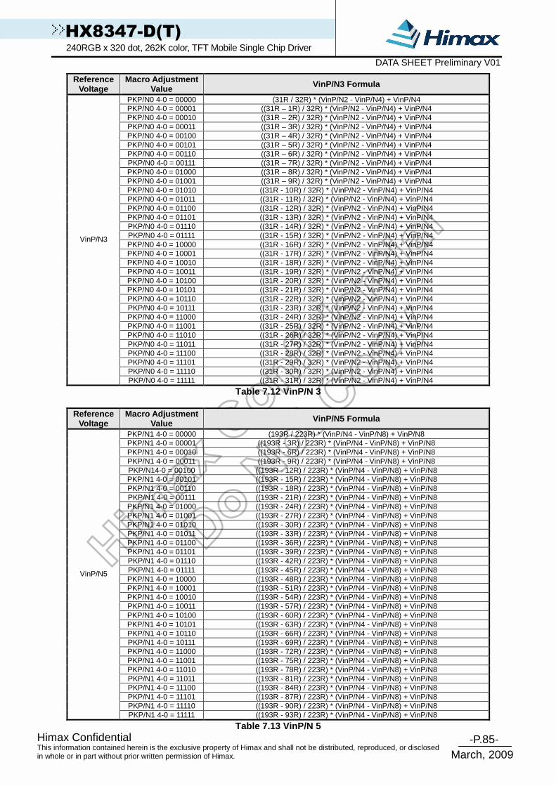
-P.85- Himax Confidential
March, 2009
This information contained herein is the exclusive property of Himax and shall not be distributed, reproduced, or disclosed in whole or in part without prior written permission of Himax.
HX8347-D(T) 240RGB x 320 dot, 262K color, TFT Mobile Single Chip Driver DATA SHEET Preliminary V01
Reference Voltage
Macro Adjustment Value VinP/N3 Formula
PKP/N0 4-0 = 00000 (31R / 32R) * (VinP/N2 - VinP/N4) + VinP/N4 PKP/N0 4-0 = 00001 ((31R – 1R) / 32R) * (VinP/N2 - VinP/N4) + VinP/N4 PKP/N0 4-0 = 00010 ((31R – 2R) / 32R) * (VinP/N2 - VinP/N4) + VinP/N4 PKP/N0 4-0 = 00011 ((31R – 3R) / 32R) * (VinP/N2 - VinP/N4) + VinP/N4 PKP/N0 4-0 = 00100 ((31R – 4R) / 32R) * (VinP/N2 - VinP/N4) + VinP/N4 PKP/N0 4-0 = 00101 ((31R – 5R) / 32R) * (VinP/N2 - VinP/N4) + VinP/N4 PKP/N0 4-0 = 00110 ((31R – 6R) / 32R) * (VinP/N2 - VinP/N4) + VinP/N4 PKP/N0 4-0 = 00111 ((31R – 7R) / 32R) * (VinP/N2 - VinP/N4) + VinP/N4 PKP/N0 4-0 = 01000 ((31R – 8R) / 32R) * (VinP/N2 - VinP/N4) + VinP/N4 PKP/N0 4-0 = 01001 ((31R – 9R) / 32R) * (VinP/N2 - VinP/N4) + VinP/N4 PKP/N0 4-0 = 01010 ((31R - 10R) / 32R) * (VinP/N2 - VinP/N4) + VinP/N4 PKP/N0 4-0 = 01011 ((31R - 11R) / 32R) * (VinP/N2 - VinP/N4) + VinP/N4 PKP/N0 4-0 = 01100 ((31R - 12R) / 32R) * (VinP/N2 - VinP/N4) + VinP/N4 PKP/N0 4-0 = 01101 ((31R - 13R) / 32R) * (VinP/N2 - VinP/N4) + VinP/N4 PKP/N0 4-0 = 01110 ((31R - 14R) / 32R) * (VinP/N2 - VinP/N4) + VinP/N4 PKP/N0 4-0 = 01111 ((31R - 15R) / 32R) * (VinP/N2 - VinP/N4) + VinP/N4 PKP/N0 4-0 = 10000 ((31R - 16R) / 32R) * (VinP/N2 - VinP/N4) + VinP/N4 PKP/N0 4-0 = 10001 ((31R - 17R) / 32R) * (VinP/N2 - VinP/N4) + VinP/N4 PKP/N0 4-0 = 10010 ((31R - 18R) / 32R) * (VinP/N2 - VinP/N4) + VinP/N4 PKP/N0 4-0 = 10011 ((31R - 19R) / 32R) * (VinP/N2 - VinP/N4) + VinP/N4 PKP/N0 4-0 = 10100 ((31R - 20R) / 32R) * (VinP/N2 - VinP/N4) + VinP/N4 PKP/N0 4-0 = 10101 ((31R - 21R) / 32R) * (VinP/N2 - VinP/N4) + VinP/N4 PKP/N0 4-0 = 10110 ((31R - 22R) / 32R) * (VinP/N2 - VinP/N4) + VinP/N4 PKP/N0 4-0 = 10111 ((31R - 23R) / 32R) * (VinP/N2 - VinP/N4) + VinP/N4 PKP/N0 4-0 = 11000 ((31R - 24R) / 32R) * (VinP/N2 - VinP/N4) + VinP/N4 PKP/N0 4-0 = 11001 ((31R - 25R) / 32R) * (VinP/N2 - VinP/N4) + VinP/N4 PKP/N0 4-0 = 11010 ((31R - 26R) / 32R) * (VinP/N2 - VinP/N4) + VinP/N4 PKP/N0 4-0 = 11011 ((31R - 27R) / 32R) * (VinP/N2 - VinP/N4) + VinP/N4 PKP/N0 4-0 = 11100 ((31R - 28R) / 32R) * (VinP/N2 - VinP/N4) + VinP/N4 PKP/N0 4-0 = 11101 ((31R - 29R) / 32R) * (VinP/N2 - VinP/N4) + VinP/N4 PKP/N0 4-0 = 11110 ((31R - 30R) / 32R) * (VinP/N2 - VinP/N4) + VinP/N4
VinP/N3
PKP/N0 4-0 = 11111 ((31R - 31R) / 32R) * (VinP/N2 - VinP/N4) + VinP/N4
Table 7.12 VinP/N 3
Reference Voltage
Macro Adjustment Value VinP/N5 Formula
PKP/N1 4-0 = 00000 (193R / 223R) * (VinP/N4 - VinP/N8) + VinP/N8 PKP/N1 4-0 = 00001 ((193R - 3R) / 223R) * (VinP/N4 - VinP/N8) + VinP/N8 PKP/N1 4-0 = 00010 ((193R - 6R) / 223R) * (VinP/N4 - VinP/N8) + VinP/N8 PKP/N1 4-0 = 00011 ((193R - 9R) / 223R) * (VinP/N4 - VinP/N8) + VinP/N8 PKP/N14-0 = 00100 ((193R - 12R) / 223R) * (VinP/N4 - VinP/N8) + VinP/N8 PKP/N1 4-0 = 00101 ((193R - 15R) / 223R) * (VinP/N4 - VinP/N8) + VinP/N8 PKP/N1 4-0 = 00110 ((193R - 18R) / 223R) * (VinP/N4 - VinP/N8) + VinP/N8 PKP/N1 4-0 = 00111 ((193R - 21R) / 223R) * (VinP/N4 - VinP/N8) + VinP/N8 PKP/N1 4-0 = 01000 ((193R - 24R) / 223R) * (VinP/N4 - VinP/N8) + VinP/N8 PKP/N1 4-0 = 01001 ((193R - 27R) / 223R) * (VinP/N4 - VinP/N8) + VinP/N8 PKP/N1 4-0 = 01010 ((193R - 30R) / 223R) * (VinP/N4 - VinP/N8) + VinP/N8 PKP/N1 4-0 = 01011 ((193R - 33R) / 223R) * (VinP/N4 - VinP/N8) + VinP/N8 PKP/N1 4-0 = 01100 ((193R - 36R) / 223R) * (VinP/N4 - VinP/N8) + VinP/N8 PKP/N1 4-0 = 01101 ((193R - 39R) / 223R) * (VinP/N4 - VinP/N8) + VinP/N8 PKP/N1 4-0 = 01110 ((193R - 42R) / 223R) * (VinP/N4 - VinP/N8) + VinP/N8 PKP/N1 4-0 = 01111 ((193R - 45R) / 223R) * (VinP/N4 - VinP/N8) + VinP/N8 PKP/N1 4-0 = 10000 ((193R - 48R) / 223R) * (VinP/N4 - VinP/N8) + VinP/N8 PKP/N1 4-0 = 10001 ((193R - 51R) / 223R) * (VinP/N4 - VinP/N8) + VinP/N8 PKP/N1 4-0 = 10010 ((193R - 54R) / 223R) * (VinP/N4 - VinP/N8) + VinP/N8 PKP/N1 4-0 = 10011 ((193R - 57R) / 223R) * (VinP/N4 - VinP/N8) + VinP/N8 PKP/N1 4-0 = 10100 ((193R - 60R) / 223R) * (VinP/N4 - VinP/N8) + VinP/N8 PKP/N1 4-0 = 10101 ((193R - 63R) / 223R) * (VinP/N4 - VinP/N8) + VinP/N8 PKP/N1 4-0 = 10110 ((193R - 66R) / 223R) * (VinP/N4 - VinP/N8) + VinP/N8 PKP/N1 4-0 = 10111 ((193R - 69R) / 223R) * (VinP/N4 - VinP/N8) + VinP/N8 PKP/N1 4-0 = 11000 ((193R - 72R) / 223R) * (VinP/N4 - VinP/N8) + VinP/N8 PKP/N1 4-0 = 11001 ((193R - 75R) / 223R) * (VinP/N4 - VinP/N8) + VinP/N8 PKP/N1 4-0 = 11010 ((193R - 78R) / 223R) * (VinP/N4 - VinP/N8) + VinP/N8 PKP/N1 4-0 = 11011 ((193R - 81R) / 223R) * (VinP/N4 - VinP/N8) + VinP/N8 PKP/N1 4-0 = 11100 ((193R - 84R) / 223R) * (VinP/N4 - VinP/N8) + VinP/N8 PKP/N1 4-0 = 11101 ((193R - 87R) / 223R) * (VinP/N4 - VinP/N8) + VinP/N8 PKP/N1 4-0 = 11110 ((193R - 90R) / 223R) * (VinP/N4 - VinP/N8) + VinP/N8
VinP/N5
PKP/N1 4-0 = 11111 ((193R - 93R) / 223R) * (VinP/N4 - VinP/N8) + VinP/N8
Table 7.13 VinP/N 5

-P.86- Himax Confidential
March, 2009
This information contained herein is the exclusive property of Himax and shall not be distributed, reproduced, or disclosed in whole or in part without prior written permission of Himax.
HX8347-D(T) 240RGB x 320 dot, 262K color, TFT Mobile Single Chip Driver DATA SHEET Preliminary V01
Reference Voltage
Macro Adjustment Value VinP/N6 Formula
PKP/N2 4-0 = 00000 (158R / 223R) * (VinP/N4 - VinP/N8) + VinP/N8 PKP/N2 4-0 = 00001 ((158R - 3R) / 223R) * (VinP/N4 - VinP/N8) + VinP/N8 PKP/N2 4-0 = 00010 ((158R - 6R) / 223R) * (VinP/N4 - VinP/N8) + VinP/N8 PKP/N2 4-0 = 00011 ((158R - 9R) / 223R) * (VinP/N4 - VinP/N8) + VinP/N8 PKP/N2 4-0 = 00100 ((158R - 12R) / 223R) * (VinP/N4 - VinP/N8) + VinP/N8 PKP/N2 4-0 = 00101 ((158R - 15R) / 223R) * (VinP/N4 - VinP/N8) + VinP/N8 PKP/N2 4-0 = 00110 ((158R - 18R) / 223R) * (VinP/N4 - VinP/N8) + VinP/N8 PKP/N2 4-0 = 00111 ((158R - 21R) / 223R) * (VinP/N4 - VinP/N8) + VinP/N8 PKP/N2 4-0 = 01000 ((158R - 24R) / 223R) * (VinP/N4 - VinP/N8) + VinP/N8 PKP/N2 4-0 = 01001 ((158R - 27R) / 223R) * (VinP/N4 - VinP/N8) + VinP/N8 PKP/N2 4-0 = 01010 ((158R - 30R) / 223R) * (VinP/N4 - VinP/N8) + VinP/N8 PKP/N2 4-0 = 01011 ((158R - 33R) / 223R) * (VinP/N4 - VinP/N8) + VinP/N8 PKP/N2 4-0 = 01100 ((158R - 36R) / 223R) * (VinP/N4 - VinP/N8) + VinP/N8 PKP/N2 4-0 = 01101 ((158R - 39R) / 223R) * (VinP/N4 - VinP/N8) + VinP/N8 PKP/N2 4-0 = 01110 ((158R - 42R) / 223R) * (VinP/N4 - VinP/N8) + VinP/N8 PKP/N2 4-0 = 01111 ((158R - 45R) / 223R) * (VinP/N4 - VinP/N8) + VinP/N8 PKP/N2 4-0 = 10000 ((158R - 48R) / 223R) * (VinP/N4 - VinP/N8) + VinP/N8 PKP/N2 4-0 = 10001 ((158R - 51R) / 223R) * (VinP/N4 - VinP/N8) + VinP/N8 PKP/N2 4-0 = 10010 ((158R - 54R) / 223R) * (VinP/N4 - VinP/N8) + VinP/N8 PKP/N2 4-0 = 10011 ((158R - 57R) / 223R) * (VinP/N4 - VinP/N8) + VinP/N8 PKP/N2 4-0 = 10100 ((158R - 60R) / 223R) * (VinP/N4 - VinP/N8) + VinP/N8 PKP/N2 4-0 = 10101 ((158R - 63R) / 223R) * (VinP/N4 - VinP/N8) + VinP/N8 PKP/N2 4-0 = 10110 ((158R - 66R) / 223R) * (VinP/N4 - VinP/N8) + VinP/N8 PKP/N2 4-0 = 10111 ((158R - 69R) / 223R) * (VinP/N4 - VinP/N8) + VinP/N8 PKP/N2 4-0 = 11000 ((158R - 72R) / 223R) * (VinP/N4 - VinP/N8) + VinP/N8 PKP/N2 4-0 = 11001 ((158R - 75R) / 223R) * (VinP/N4 - VinP/N8) + VinP/N8 PKP/N2 4-0 = 11010 ((158R - 78R) / 223R) * (VinP/N4 - VinP/N8) + VinP/N8 PKP/N2 4-0 = 11011 ((158R - 81R) / 223R) * (VinP/N4 - VinP/N8) + VinP/N8 PKP/N2 4-0 = 11100 ((158R - 84R) / 223R) * (VinP/N4 - VinP/N8) + VinP/N8 PKP/N2 4-0 = 11101 ((158R - 87R) / 223R) * (VinP/N4 - VinP/N8) + VinP/N8 PKP/N2 4-0 = 11110 ((158R - 90R) / 223R) * (VinP/N4 - VinP/N8) + VinP/N8
VinP/N6
PKP/N2 4-0 = 11111 ((158R - 93R) / 223R) * (VinP/N4 - VinP/N8) + VinP/N8
Table 7.14 VinP/N 6
Reference Voltage
Macro Adjustment Value VinP/N7 Formula
PKP/N3 4-0 = 00000 (123R / 223R) * (VinP/N4 - VinP/N8) + VinP/N8 PKP/N3 4-0 = 00001 ((123R - 3R) / 223R) * (VinP/N4 - VinP/N8) + VinP/N8 PKP/N3 4-0 = 00010 ((123R - 6R) / 223R) * (VinP/N4 - VinP/N8) + VinP/N8 PKP/N3 4-0 = 00011 ((123R - 9R) / 223R) * (VinP/N4 - VinP/N8) + VinP/N8 PKP/N3 4-0 = 00100 ((123R - 12R) / 223R) * (VinP/N4 - VinP/N8) + VinP/N8 PKP/N3 4-0 = 00101 ((123R - 15R) / 223R) * (VinP/N4 - VinP/N8) + VinP/N8 PKP/N3 4-0 = 00110 ((123R - 18R) / 223R) * (VinP/N4 - VinP/N8) + VinP/N8 PKP/N3 4-0 = 00111 ((123R - 21R) / 223R) * (VinP/N4 - VinP/N8) + VinP/N8 PKP/N3 4-0 = 01000 ((123R - 24R) / 223R) * (VinP/N4 - VinP/N8) + VinP/N8 PKP/N3 4-0 = 01001 ((123R - 27R) / 223R) * (VinP/N4 - VinP/N8) + VinP/N8 PKP/N3 4-0 = 01010 ((123R - 30R) / 223R) * (VinP/N4 - VinP/N8) + VinP/N8 PKP/N3 4-0 = 01011 ((123R - 33R) / 223R) * (VinP/N4 - VinP/N8) + VinP/N8 PKP/N3 4-0 = 01100 ((123R - 36R) / 223R) * (VinP/N4 - VinP/N8) + VinP/N8 PKP/N3 4-0 = 01101 ((123R - 39R) / 223R) * (VinP/N4 - VinP/N8) + VinP/N8 PKP/N3 4-0 = 01110 ((123R - 42R) / 223R) * (VinP/N4 - VinP/N8) + VinP/N8 PKP/N3 4-0 = 01111 ((123R - 45R) / 223R) * (VinP/N4 - VinP/N8) + VinP/N8 PKP/N3 4-0 = 10000 ((123R - 48R) / 223R) * (VinP/N4 - VinP/N8) + VinP/N8 PKP/N3 4-0 = 10001 ((123R - 51R) / 223R) * (VinP/N4 - VinP/N8) + VinP/N8 PKP/N3 4-0 = 10010 ((123R - 54R) / 223R) * (VinP/N4 - VinP/N8) + VinP/N8 PKP/N3 4-0 = 10011 ((123R - 57R) / 223R) * (VinP/N4 - VinP/N8) + VinP/N8 PKP/N3 4-0 = 10100 ((123R - 60R) / 223R) * (VinP/N4 - VinP/N8) + VinP/N8 PKP/N3 4-0 = 10101 ((123R - 63R) / 223R) * (VinP/N4 - VinP/N8) + VinP/N8 PKP/N3 4-0 = 10110 ((123R - 66R) / 223R) * (VinP/N4 - VinP/N8) + VinP/N8 PKP/N3 4-0 = 10111 ((123R - 69R) / 223R) * (VinP/N4 - VinP/N8) + VinP/N8 PKP/N3 4-0 = 11000 ((123R - 72R) / 223R) * (VinP/N4 - VinP/N8) + VinP/N8 PKP/N3 4-0 = 11001 ((123R - 75R) / 223R) * (VinP/N4 - VinP/N8) + VinP/N8 PKP/N3 4-0 = 11010 ((123R - 78R) / 223R) * (VinP/N4 - VinP/N8) + VinP/N8 PKP/N3 4-0 = 11011 ((123R - 81R) / 223R) * (VinP/N4 - VinP/N8) + VinP/N8 PKP/N3 4-0 = 11100 ((123R - 84R) / 223R) * (VinP/N4 - VinP/N8) + VinP/N8 PKP/N3 4-0 = 11101 ((123R - 87R) / 223R) * (VinP/N4 - VinP/N8) + VinP/N8 PKP/N3 4-0 = 11110 ((123R - 90R) / 223R) * (VinP/N4 - VinP/N8) + VinP/N8
VinP/N7
PKP/N3 4-0 = 11111 ((123R - 93R) / 223R) * (VinP/N4 - VinP/N8) + VinP/N8
Table 7.15 VinP/N 7

-P.87- Himax Confidential
March, 2009
This information contained herein is the exclusive property of Himax and shall not be distributed, reproduced, or disclosed in whole or in part without prior written permission of Himax.
HX8347-D(T) 240RGB x 320 dot, 262K color, TFT Mobile Single Chip Driver DATA SHEET Preliminary V01
Reference
Voltage Macro Adjustment
Value VinP/N9 Formula
PKP/N4 4-0 = 00000 (31R / 32R) * (VinP/N8 - VinP/N10) + VinP/N10 PKP/N4 4-0 = 00001 ((31R - 1R) / 32R) * (VinP/N8 - VinP/N10) + VinP/N10 PKP/N4 4-0 = 00010 ((31R - 2R) / 32R) * (VinP/N8 - VinP/N10) + VinP/N10 PKP/N4 4-0 = 00011 ((31R - 3R) / 32R) * (VinP/N8 - VinP/N10) + VinP/N10 PKP/N4 4-0 = 00100 ((31R - 4R) / 32R) * (VinP/N8 - VinP/N10) + VinP/N10 PKP/N4 4-0 = 00101 ((31R - 5R) / 32R) * (VinP/N8 - VinP/N10) + VinP/N10 PKP/N4 4-0 = 00110 ((31R - 6R) / 32R) * (VinP/N8 - VinP/N10) + VinP/N10 PKP/N4 4-0 = 00111 ((31R - 7R) / 32R) * (VinP/N8 - VinP/N10) + VinP/N10 PKP/N4 4-0 = 01000 ((31R - 8R) / 32R) * (VinP/N8 - VinP/N10) + VinP/N10 PKP/N4 4-0 = 01001 ((31R - 9R) / 32R) * (VinP/N8 - VinP/N10) + VinP/N10 PKP/N4 4-0 = 01010 ((31R - 10R) / 32R) * (VinP/N8 - VinP/N10) + VinP/N10 PKP/N4 4-0 = 01011 ((31R - 11R) / 32R) * (VinP/N8 - VinP/N10) + VinP/N10 PKP/N4 4-0 = 01100 ((31R - 12R) / 32R) * (VinP/N8 - VinP/N10) + VinP/N10 PKP/N4 4-0 = 01101 ((31R - 13R) / 32R) * (VinP/N8 - VinP/N10) + VinP/N10 PKP/N4 4-0 = 01110 ((31R - 14R) / 32R) * (VinP/N8 - VinP/N10) + VinP/N10 PKP/N4 4-0 = 01111 ((31R - 15R) / 32R) * (VinP/N8 - VinP/N10) + VinP/N10 PKP/N4 4-0 = 10000 ((31R - 16R) / 32R) * (VinP/N8 - VinP/N10) + VinP/N10 PKP/N4 4-0 = 10001 ((31R - 17R) / 32R) * (VinP/N8 - VinP/N10) + VinP/N10 PKP/N4 4-0 = 10010 ((31R - 18R) / 32R) * (VinP/N8 - VinP/N10) + VinP/N10 PKP/N4 4-0 = 10011 ((31R - 19R) / 32R) * (VinP/N8 - VinP/N10) + VinP/N10 PKP/N4 4-0 = 10100 ((31R - 20R) / 32R) * (VinP/N8 - VinP/N10) + VinP/N10 PKP/N4 4-0 = 10101 ((31R - 21R) / 32R) * (VinP/N8 - VinP/N10) + VinP/N10 PKP/N4 4-0 = 10110 ((31R - 22R) / 32R) * (VinP/N8 - VinP/N10) + VinP/N10 PKP/N4 4-0 = 10111 ((31R - 23R) / 32R) * (VinP/N8 - VinP/N10) + VinP/N10 PKP/N4 4-0 = 11000 ((31R - 24R) / 32R) * (VinP/N8 - VinP/N10) + VinP/N10 PKP/N4 4-0 = 11001 ((31R - 25R) / 32R) * (VinP/N8 - VinP/N10) + VinP/N10 PKP/N4 4-0 = 11010 ((31R - 26R) / 32R) * (VinP/N8 - VinP/N10) + VinP/N10 PKP/N4 4-0 = 11011 ((31R - 27R) / 32R) * (VinP/N8 - VinP/N10) + VinP/N10 PKP/N4 4-0 = 11100 ((31R - 28R) / 32R) * (VinP/N8 - VinP/N10) + VinP/N10 PKP/N4 4-0 = 11101 ((31R - 29R) / 32R) * (VinP/N8 - VinP/N10) + VinP/N10 PKP/N4 4-0 = 11110 ((31R - 30R) / 32R) * (VinP/N8 - VinP/N10) + VinP/N10
VinP/N9
PKP/N4 4-0 = 11111 ((31R - 31R) / 32R) * (VinP/N8 - VinP/N10) + VinP/N10
Table 7.16 VinP/N 9

-P.88- Himax Confidential
March, 2009
This information contained herein is the exclusive property of Himax and shall not be distributed, reproduced, or disclosed in whole or in part without prior written permission of Himax.
HX8347-D(T) 240RGB x 320 dot, 262K color, TFT Mobile Single Chip Driver DATA SHEET Preliminary V01
Grayscale
Voltage Formula Grayscale Voltage Formula
V0 VinP0 V32 VinP6 V1 VinP1 V33 VinP7+(VinP6- VinP7)*(20R/22R) V2 VinP2 V34 VinP7+(VinP6- VinP7)*(18R/22R) V3 VinP3 V35 VinP7+(VinP6- VinP7)*(16R/22R) V4 VinP4+ (VinP3 - VinP4)*CT1 V36 VinP7+(VinP6- VinP7)*(14R/22R) V5 VinP4+ (VinP3 - VinP4)*CT2 V37 VinP7+(VinP6- VinP7)*(12R/22R) V6 VinP4+ (VinP3 - VinP4)*CT3 V38 VinP7+(VinP6- VinP7)*(10R/22R) V7 VinP4+ (VinP3 - VinP4)*CT4 V39 VinP7+(VinP6- VinP7)*(8R/22R) V8 VinP4 V40 VinP7+(VinP6- VinP7)*(6R/22R) V9 VinP5+(VinP4- VinP5)*(22R/24R) V41 VinP7+(VinP6- VinP7)*(4R/22R) V10 VinP5+(VinP4- VinP5)*(20R/24R) V42 VinP7+(VinP6- VinP7)*(2R/22R) V11 VinP5+(VinP4- VinP5)*(18R/24R) V43 VinP7 V12 VinP5+(VinP4- VinP5)*(16R/24R) V44 VinP8+(VinP7- VinP8)*(22R/24R) V13 VinP5+(VinP4- VinP5)*(14R/24R) V45 VinP8+(VinP7- VinP8)*(20R/24R) V14 VinP5+(VinP4- VinP5)*(12R/24R) V46 VinP8+(VinP7- VinP8)*(18R/24R) V15 VinP5+(VinP4- VinP5)*(10R/24R) V47 VinP8+(VinP7- VinP8)*(16R/24R) V16 VinP5+(VinP4- VinP5)*(8R/24R) V48 VinP8+(VinP7- VinP8)*(14R/24R) V17 VinP5+(VinP4- VinP5)*(6R/24R) V49 VinP8+(VinP7- VinP8)*(12R/24R) V18 VinP5+(VinP4- VinP5)*(4R/24R) V50 VinP8+(VinP7- VinP8)*(10R/24R) V19 VinP5+(VinP4- VinP5)*(2R/24R) V51 VinP8+(VinP7- VinP8)*(8R/24R) V20 VinP5 V52 VinP8+(VinP7- VinP8)*(6R/24R) V21 VinP6+(VinP5- VinP6)*(22R/24R) V53 VinP8+(VinP7- VinP8)*(4R/24R) V22 VinP6+(VinP5- VinP6)*(20R/24R) V54 VinP8+(VinP7- VinP8)*(2R/24R) V23 VinP6+(VinP5- VinP6)*(18R/24R) V55 VinP8 V24 VinP6+(VinP5- VinP6)*(16R/24R) V56 VinP9+ (VinP8 – VinP9)*CB1 V25 VinP6+(VinP5- VinP6)*(14R/24R) V57 VinP9+ (VinP8 – VinP9)*CB2 V26 VinP6+(VinP5- VinP6)*(12R/24R) V58 VinP9+ (VinP8 – VinP9)*CB3 V27 VinP6+(VinP5- VinP6)*(10R/24R) V59 VinP9+ (VinP8 – VinP9)*CB4 V28 VinP6+(VinP5- VinP6)*(8R/24R) V60 VinP9 V29 VinP6+(VinP5- VinP6)*(6R/24R) V61 VinP10 V30 VinP6+(VinP5- VinP6)*(4R/24R) V62 VinP11 V31 VinP6+(VinP5- VinP6)*(2R/24R) V63 VinP12
Table 7.17 Voltage calculation formula of 64-graysc ale voltage (positive polarity)
CGMP0[1:0] “00” “01” “10” “11” CGMP1[1:0] “00” “01” “10” “11” CT1 3/4 28/45 26/33 3/4 CB1 4/5 18/19 44/47 17/20 CT2 1/2 4/15 6/11 21/40 CB2 3/5 50/57 40/47 27/40 CT3 7/24 7/45 10/33 13/40 CB3 2/5 15/19 35/47 19/40 CT4 1/8 1/15 1/6 3/20
CB4 1/5 23/57 28/47 1/4 Table 7.18 Voltage calculation formula of grayscale voltage V4~V7 and V56~V59
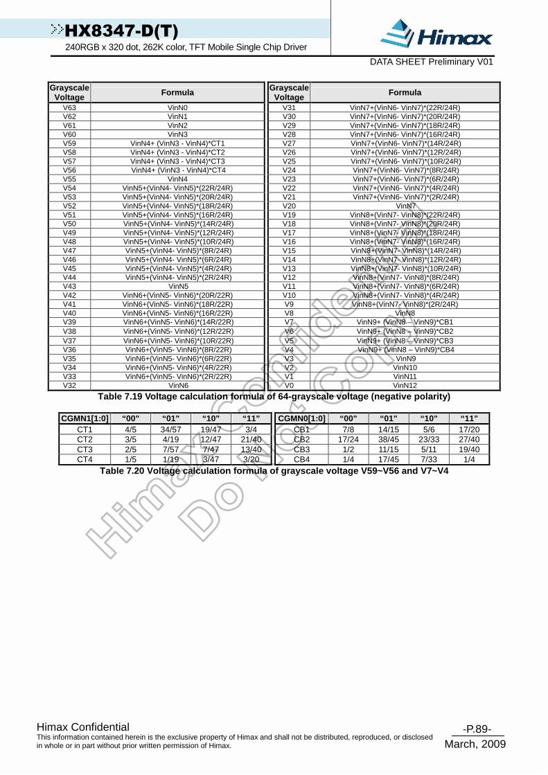
-P.89- Himax Confidential
March, 2009
This information contained herein is the exclusive property of Himax and shall not be distributed, reproduced, or disclosed in whole or in part without prior written permission of Himax.
HX8347-D(T) 240RGB x 320 dot, 262K color, TFT Mobile Single Chip Driver DATA SHEET Preliminary V01
Grayscale
Voltage Formula Grayscale Voltage Formula
V63 VinN0 V31 VinN7+(VinN6- VinN7)*(22R/24R) V62 VinN1 V30 VinN7+(VinN6- VinN7)*(20R/24R) V61 VinN2 V29 VinN7+(VinN6- VinN7)*(18R/24R) V60 VinN3 V28 VinN7+(VinN6- VinN7)*(16R/24R) V59 VinN4+ (VinN3 - VinN4)*CT1 V27 VinN7+(VinN6- VinN7)*(14R/24R) V58 VinN4+ (VinN3 - VinN4)*CT2 V26 VinN7+(VinN6- VinN7)*(12R/24R) V57 VinN4+ (VinN3 - VinN4)*CT3 V25 VinN7+(VinN6- VinN7)*(10R/24R) V56 VinN4+ (VinN3 - VinN4)*CT4 V24 VinN7+(VinN6- VinN7)*(8R/24R) V55 VinN4 V23 VinN7+(VinN6- VinN7)*(6R/24R) V54 VinN5+(VinN4- VinN5)*(22R/24R) V22 VinN7+(VinN6- VinN7)*(4R/24R) V53 VinN5+(VinN4- VinN5)*(20R/24R) V21 VinN7+(VinN6- VinN7)*(2R/24R) V52 VinN5+(VinN4- VinN5)*(18R/24R) V20 VinN7 V51 VinN5+(VinN4- VinN5)*(16R/24R) V19 VinN8+(VinN7- VinN8)*(22R/24R) V50 VinN5+(VinN4- VinN5)*(14R/24R) V18 VinN8+(VinN7- VinN8)*(20R/24R) V49 VinN5+(VinN4- VinN5)*(12R/24R) V17 VinN8+(VinN7- VinN8)*(18R/24R) V48 VinN5+(VinN4- VinN5)*(10R/24R) V16 VinN8+(VinN7- VinN8)*(16R/24R) V47 VinN5+(VinN4- VinN5)*(8R/24R) V15 VinN8+(VinN7- VinN8)*(14R/24R) V46 VinN5+(VinN4- VinN5)*(6R/24R) V14 VinN8+(VinN7- VinN8)*(12R/24R) V45 VinN5+(VinN4- VinN5)*(4R/24R) V13 VinN8+(VinN7- VinN8)*(10R/24R) V44 VinN5+(VinN4- VinN5)*(2R/24R) V12 VinN8+(VinN7- VinN8)*(8R/24R) V43 VinN5 V11 VinN8+(VinN7- VinN8)*(6R/24R) V42 VinN6+(VinN5- VinN6)*(20R/22R) V10 VinN8+(VinN7- VinN8)*(4R/24R) V41 VinN6+(VinN5- VinN6)*(18R/22R) V9 VinN8+(VinN7- VinN8)*(2R/24R) V40 VinN6+(VinN5- VinN6)*(16R/22R) V8 VinN8 V39 VinN6+(VinN5- VinN6)*(14R/22R) V7 VinN9+ (VinN8 – VinN9)*CB1 V38 VinN6+(VinN5- VinN6)*(12R/22R) V6 VinN9+ (VinN8 – VinN9)*CB2 V37 VinN6+(VinN5- VinN6)*(10R/22R) V5 VinN9+ (VinN8 – VinN9)*CB3 V36 VinN6+(VinN5- VinN6)*(8R/22R) V4 VinN9+ (VinN8 – VinN9)*CB4 V35 VinN6+(VinN5- VinN6)*(6R/22R) V3 VinN9 V34 VinN6+(VinN5- VinN6)*(4R/22R) V2 VinN10 V33 VinN6+(VinN5- VinN6)*(2R/22R) V1 VinN11 V32 VinN6 V0 VinN12
Table 7.19 Voltage calculation formula of 64-graysc ale voltage (negative polarity)
CGMN1[1:0] “00” “01” “10” “11” CGMN0[1:0] “00” “01” “10” “11” CT1 4/5 34/57 19/47 3/4 CB1 7/8 14/15 5/6 17/20 CT2 3/5 4/19 12/47 21/40 CB2 17/24 38/45 23/33 27/40 CT3 2/5 7/57 7/47 13/40 CB3 1/2 11/15 5/11 19/40 CT4 1/5 1/19 3/47 3/20
CB4 1/4 17/45 7/33 1/4 Table 7.20 Voltage calculation formula of grayscale voltage V59~V56 and V7~V4

-P.90- Himax Confidential
March, 2009
This information contained herein is the exclusive property of Himax and shall not be distributed, reproduced, or disclosed in whole or in part without prior written permission of Himax.
HX8347-D(T) 240RGB x 320 dot, 262K color, TFT Mobile Single Chip Driver DATA SHEET Preliminary V01
Relationship between GRAM data and output level (“N ormally White Panel”, GRAM data=0)
Figure 7.4 Relationship between source output and V com
Negative polarity
Positive polarity
000000 111111RAM Data
(Same characteristic for each RGB)
V63
V0
Output Level
Figure 7.5 Relationship between GRAM data and outpu t level (normal white panel REV_Panel=“0”)
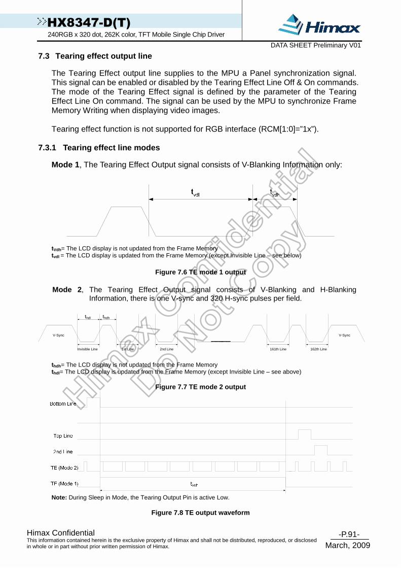
-P.91- Himax Confidential
March, 2009
This information contained herein is the exclusive property of Himax and shall not be distributed, reproduced, or disclosed in whole or in part without prior written permission of Himax.
HX8347-D(T) 240RGB x 320 dot, 262K color, TFT Mobile Single Chip Driver DATA SHEET Preliminary V01
7.3 Tearing effect output line The Tearing Effect output line supplies to the MPU a Panel synchronization signal. This signal can be enabled or disabled by the Tearing Effect Line Off & On commands. The mode of the Tearing Effect signal is defined by the parameter of the Tearing Effect Line On command. The signal can be used by the MPU to synchronize Frame Memory Writing when displaying video images. Tearing effect function is not supported for RGB interface (RCM[1:0]=”1x”).
7.3.1 Tearing effect line modes
Mode 1 , The Tearing Effect Output signal consists of V-Blanking Information only:
tVdh= The LCD display is not updated from the Frame Memory tvdl = The LCD display is updated from the Frame Memory (except Invisible Line – see below)
Figure 7.6 TE mode 1 output
Mode 2 , The Tearing Effect Output signal consists of V-Blanking and H-Blanking
Information, there is one V-sync and 320 H-sync pulses per field.
V-Sync
Invisible Line 1st Line 2nd Line
thdl thdh
V-Sync
161th Line 162th Line
thdh= The LCD display is not updated from the Frame Memory thdl= The LCD display is updated from the Frame Memory (except Invisible Line – see above)
Figure 7.7 TE mode 2 output
Note: During Sleep in Mode, the Tearing Output Pin is active Low.
Figure 7.8 TE output waveform
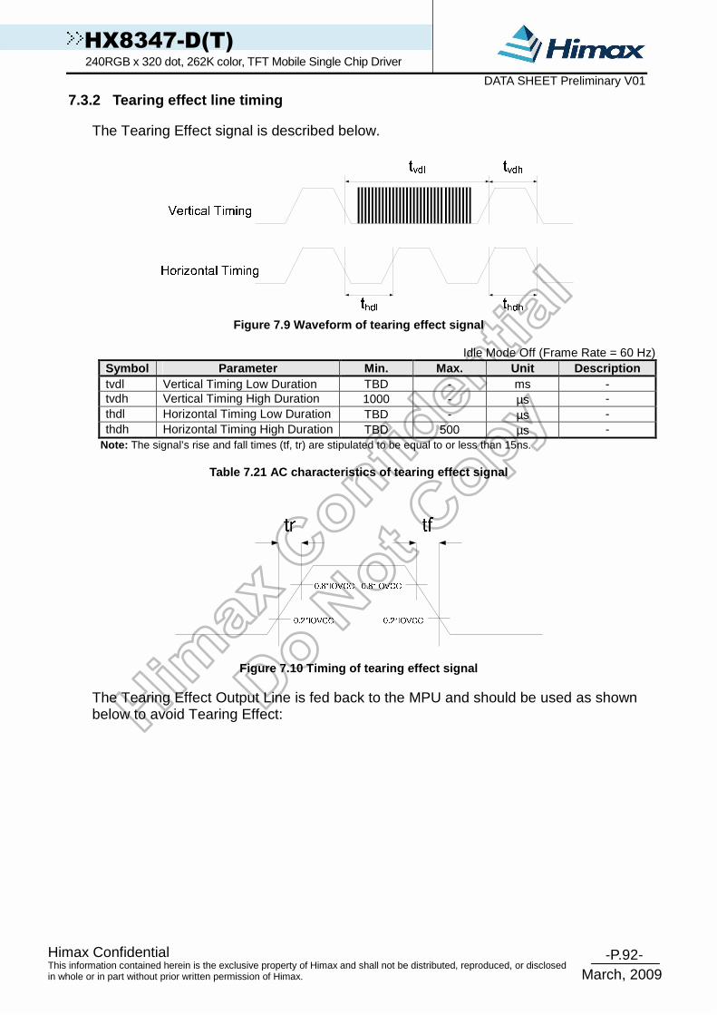
-P.92- Himax Confidential
March, 2009
This information contained herein is the exclusive property of Himax and shall not be distributed, reproduced, or disclosed in whole or in part without prior written permission of Himax.
HX8347-D(T) 240RGB x 320 dot, 262K color, TFT Mobile Single Chip Driver DATA SHEET Preliminary V01
7.3.2 Tearing effect line timing
The Tearing Effect signal is described below.
Figure 7.9 Waveform of tearing effect signal
Idle Mode Off (Frame Rate = 60 Hz)
Symbol Parameter Min. Max. Unit Description tvdl Vertical Timing Low Duration TBD - ms - tvdh Vertical Timing High Duration 1000 - µs - thdl Horizontal Timing Low Duration TBD - µs - thdh Horizontal Timing High Duration TBD 500 µs -
Note: The signal’s rise and fall times (tf, tr) are stipulated to be equal to or less than 15ns.
Table 7.21 AC characteristics of tearing effect sig nal
Figure 7.10 Timing of tearing effect signal The Tearing Effect Output Line is fed back to the MPU and should be used as shown below to avoid Tearing Effect:
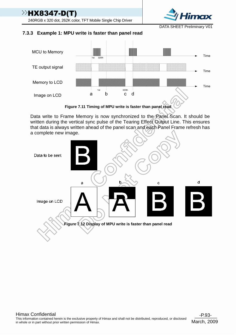
-P.93- Himax Confidential
March, 2009
This information contained herein is the exclusive property of Himax and shall not be distributed, reproduced, or disclosed in whole or in part without prior written permission of Himax.
HX8347-D(T) 240RGB x 320 dot, 262K color, TFT Mobile Single Chip Driver DATA SHEET Preliminary V01
7.3.3 Example 1: MPU write is faster than panel rea d
Time
Time
Time
MCU to Memory
TE output signal
Memory to LCD
Image on LCD a b c d1st 320th
1st 320th
Figure 7.11 Timing of MPU write is faster than pane l read
Data write to Frame Memory is now synchronized to the Panel Scan. It should be written during the vertical sync pulse of the Tearing Effect Output Line. This ensures that data is always written ahead of the panel scan and each Panel Frame refresh has a complete new image.
Figure 7.12 Display of MPU write is faster than pan el read

-P.94- Himax Confidential
March, 2009
This information contained herein is the exclusive property of Himax and shall not be distributed, reproduced, or disclosed in whole or in part without prior written permission of Himax.
HX8347-D(T) 240RGB x 320 dot, 262K color, TFT Mobile Single Chip Driver DATA SHEET Preliminary V01
7.3.4 Example 2: MPU write is slower than panel rea d
Time
Time
Time
MCU to Memory
TE output signal
Memory to LCD
Image on LCD a b c d1st 320th
1st 320th
e f
Figure 7.13 Timing of MPU write is slower than pane l read
The MPU to Frame Memory write begins just after Panel Read has commenced i.e. after one horizontal sync pulse of the Tearing Effect Output Line. This allows time for the image to download behind the Panel Read pointer and finishing download during the subsequent Frame before the Read Pointer “catches” the MPU to Frame memory write position.
Figure 7.14 Display of MPU write is slower than pan el read

-P.95- Himax Confidential
March, 2009
This information contained herein is the exclusive property of Himax and shall not be distributed, reproduced, or disclosed in whole or in part without prior written permission of Himax.
HX8347-D(T) 240RGB x 320 dot, 262K color, TFT Mobile Single Chip Driver DATA SHEET Preliminary V01
7.4 Content Adaptive Brightness Control (CABC) func tion The HX8347-D has support Content Adaptive Brightness Control (CABC) Function and will output one PWM signal to external LED Driver IC. The PWM signal is automatics adjust output duty by display image for saving LED backlight power consumption. Example: Image A: -20% brightness reduction Image B: -30% brightness reduction Image C: -10% brightness reduction
Transition
time
50%
0%
100%
Time
80%
70%
90%
Transition
time
Transition
time
Image A:
Brightness
reduction
ratio -20%
Image B:
Brightness
reduction
ratio -30%
Image C:
Brightness
reduction
ratio -10%
Figure 7.15 Example of CABC function
The general block diagram of the CABC and the brightness control is illustrated below:
Image Data
PWM_CLK
(foscD)
Display Control Signal Generator
Display Data Generator
Brightness Control
BlockCABC_PWM_OUT
( BL = 1`)PWM Clock Devider
DBV[7:0]( BL = 0`)
Display Data Contents Analysis
CABC Gain / Duty
CABC Block CABC Block CABC Block CABC Block
BCTRL='0': OffBCTRL='1': On
C[1:0]='00': OffC[1:0]='01','10','11': On
Gain
Duty
VSYNC, HSYNC, ENABLE,
DCLK ( in RGB I/F)
Figure 7.16 CABC block diagram
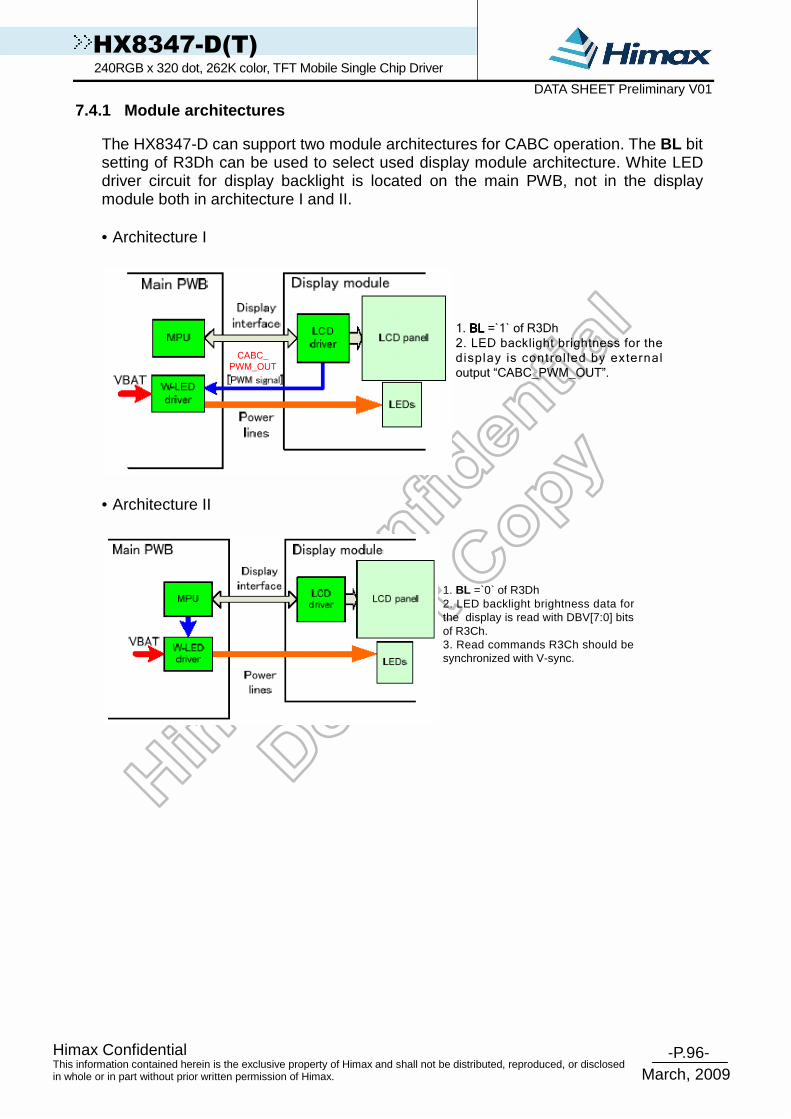
-P.96- Himax Confidential
March, 2009
This information contained herein is the exclusive property of Himax and shall not be distributed, reproduced, or disclosed in whole or in part without prior written permission of Himax.
HX8347-D(T) 240RGB x 320 dot, 262K color, TFT Mobile Single Chip Driver DATA SHEET Preliminary V01
7.4.1 Module architectures
The HX8347-D can support two module architectures for CABC operation. The BL bit setting of R3Dh can be used to select used display module architecture. White LED driver circuit for display backlight is located on the main PWB, not in the display module both in architecture I and II.
• Architecture I
CABC_
PWM_OUT
1. BLBLBLBL =`1` of R3Dh
2. LED backlight brightness for the
display is control led by external
output “CABC_PWM_OUT”.
• Architecture II
1. BL =`0` of R3Dh2. LED backlight brightness data for the display is read with DBV[7:0] bits of R3Ch.3. Read commands R3Ch should be synchronized with V-sync.

-P.97- Himax Confidential
March, 2009
This information contained herein is the exclusive property of Himax and shall not be distributed, reproduced, or disclosed in whole or in part without prior written permission of Himax.
HX8347-D(T) 240RGB x 320 dot, 262K color, TFT Mobile Single Chip Driver DATA SHEET Preliminary V01
7.4.2 Brightness control block
There is an external output signal from brightness block, CABC_PWM_OUT, to control the LED driver IC in order to control display brightness.
There are resister bits, DBV[7:0] of R3Ch, for display brightness of manual brightness setting. The CABC_PWM_OUT duty is calculated as DBV[7:0]/255 x CABC duty (generated after one-frame display data content analysis).
For example: CABC_PWM_OUT period = 2.95 ms, and DBV[7:0](R3Ch) = ‘228DEC’ and CABC duty is 74%. Then CABC_PWM_OUT duty = 228 / 255 x 74% ≡ 65.90%. Correspond to the CABC_PWM_OUT period = 2.95 ms, the high-level of CABC_PWM_OUT (high effective) = 1.94ms, and the low-level of CABC_PWM_OUT = 1.01ms.
ON
OFF
CABC_
PWM_OUT
Duty = 100%
MaximumDuty = 33% Duty = 65.90% Duty = 100%
OFF
One Period
Display
Brightness
Figure 7.17 CABC_PWM_OUT output duty
When Architecture II module is used (BL=’0’) with the example below, the CABC_PWM_OUT is always output low and the DBV[7:0](R3Ch) will be read a value as 169DEC (169/255≡ 66.27%).

-P.98- Himax Confidential
March, 2009
This information contained herein is the exclusive property of Himax and shall not be distributed, reproduced, or disclosed in whole or in part without prior written permission of Himax.
HX8347-D(T) 240RGB x 320 dot, 262K color, TFT Mobile Single Chip Driver DATA SHEET Preliminary V01
7.4.3 Minimum brightness setting of CABC function
CABC function is automatically reduced backlight brightness based on image contents. In the case of the combination with the CABC or manual brightness setting, display brightness is too dark. It must affect image quality degradation. CABC minimum brightness setting (CMB[7:0] bits of R3Fh) works to avoid too much brightness reduction. When CABC is active, CABC can not reduce the display brightness to less than CABC minimum brightness setting. Image processing function works as normal, even if the brightness can not be changed. This function does not affect the other function, manual brightness setting. Manual brightness can be set the display brightness to less than CABC minimum brightness. Smooth transition and dimming function can work as normal. When display brightness is turned off (BCTRL=’0’ of R3Dh), CABC minimum brightness setting is ignored. Read CABC minimum brightness CMB[7:0] (R3Fh) always reads the setting value.
7.4.4 Display dimming
A dimming function (how fast to change the brightness from old to new level and what are brightness levels during the change) is used when changing from one brightness level to another to avoid flicker in the actual display module. This dimming function curve is the same in increment and decrement directions.
Figure 7.18 Dimming function
Luminance Luminance Dimming Hysteresis Step Up
Time Time Without Dimming With Dimming

-P.99- Himax Confidential
March, 2009
This information contained herein is the exclusive property of Himax and shall not be distributed, reproduced, or disclosed in whole or in part without prior written permission of Himax.
HX8347-D(T) 240RGB x 320 dot, 262K color, TFT Mobile Single Chip Driver DATA SHEET Preliminary V01
7.5 LCD power generation circuit
7.5.1 Power supply circuit
The power circuit of HX8347-D is used to generate supply voltages for LCD panel driving.
Step up Circuit 1
C11P
C11N
DDVDH
Step up Circuit 3
VCL
CCCC3333
CCCC1111
CCCC9999
ReferenceVoltage
GenerationCircuit
C12P
C12N
CCCC2222
VREG1
Step up
Circuit 2
C21N
C21P
CCCC4444
C22P
C22N
CCCC5555
VGH CCCC6666
VGL CCCC7777
C31P
C31N
CCCC8888
VDDDCCCC10101010
ReferenceVoltage
GenerationCircuit
ReferenceVoltage
GenerationCircuit
VCIVCIVCIVCI
VSSAVSSAVSSAVSSA
VSSDVSSDVSSDVSSD
DDVDH
Figure 7.19 Block diagram of HX8347-D power circuit

-P.100- Himax Confidential
March, 2009
This information contained herein is the exclusive property of Himax and shall not be distributed, reproduced, or disclosed in whole or in part without prior written permission of Himax.
HX8347-D(T) 240RGB x 320 dot, 262K color, TFT Mobile Single Chip Driver DATA SHEET Preliminary V01
Specification of connected passive component
Capacitor Recommended voltage Capacity C1 (C11P/N) 6V 1µF (B characteristics) C2 (C12P/N) 6V 1µF (B characteristics) C3 (DDVDH) 10V 1µF (B characteristics) C4 (C21P/N) 10V 1µF (B characteristics) C5 (C22P/N) 10V 1µF (B characteristics) C6 (VGH) 25V 1µF (B characteristics) C7 (VGL) 16V 1µF (B characteristics) C8 (C31P/N) 6V 1µF (B characteristics) C9 (VCL) 6V 1µF (B characteristics) C10(VDDD) 6V 1µF (B characteristics)
Table 7.22 Adoptability of capacitor

-P.101- Himax Confidential
March, 2009
This information contained herein is the exclusive property of Himax and shall not be distributed, reproduced, or disclosed in whole or in part without prior written permission of Himax.
HX8347-D(T) 240RGB x 320 dot, 262K color, TFT Mobile Single Chip Driver DATA SHEET Preliminary V01
7.5.2 LCD power generation scheme
The boost voltage generated is shown as below.
VSSA, VSSD (0V)
VREG1 (3.3V ~5.8V)
VCOMH
VGH(2DDVDH~3DD
VDH)
VCOML
VCL
VGH
x (-1)
VCI (2.3 ~ 3.3V)
DDVDHDDVDH
VGL(-VCI-2DDVDH~
-VCI-DDVDH)
DC/DC
DC/DC
DC/DC
DC/DC
VGL
VCOML
VCOMH
VREG1
Register / Voltage mapping
Figure 7.20 LCD power generation scheme
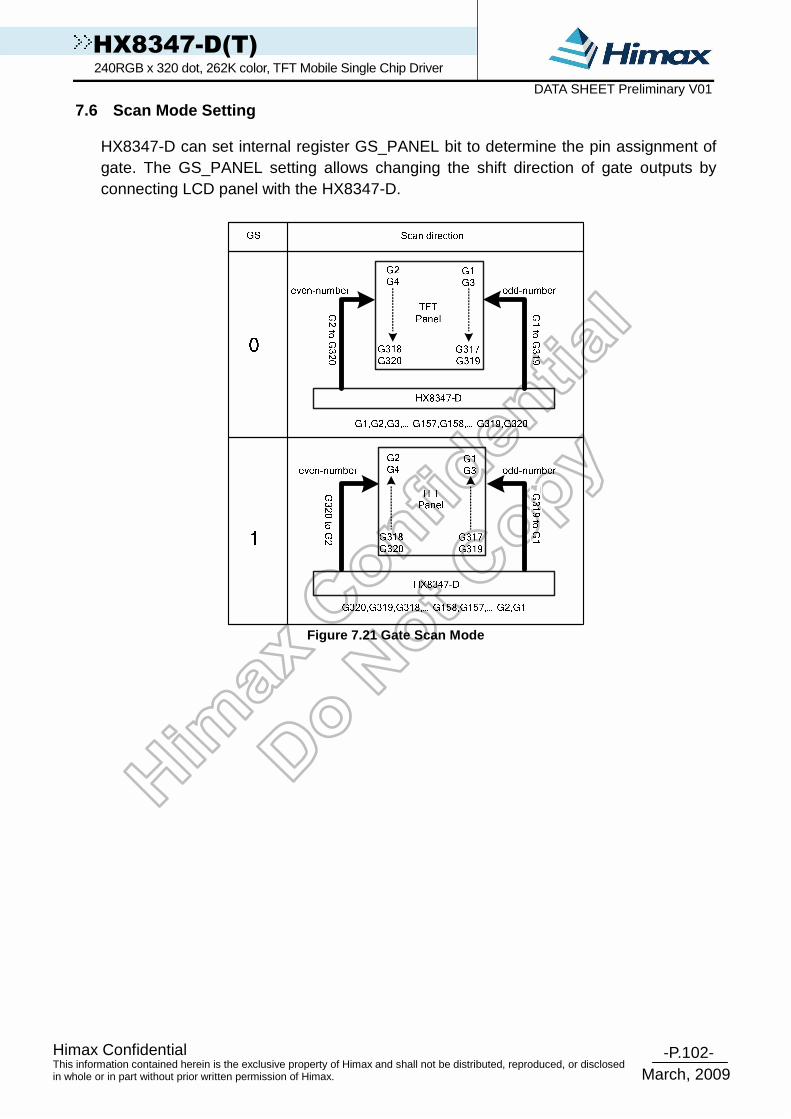
-P.102- Himax Confidential
March, 2009
This information contained herein is the exclusive property of Himax and shall not be distributed, reproduced, or disclosed in whole or in part without prior written permission of Himax.
HX8347-D(T) 240RGB x 320 dot, 262K color, TFT Mobile Single Chip Driver DATA SHEET Preliminary V01
7.6 Scan Mode Setting
HX8347-D can set internal register GS_PANEL bit to determine the pin assignment of gate. The GS_PANEL setting allows changing the shift direction of gate outputs by connecting LCD panel with the HX8347-D.
Figure 7.21 Gate Scan Mode

-P.103- Himax Confidential
March, 2009
This information contained herein is the exclusive property of Himax and shall not be distributed, reproduced, or disclosed in whole or in part without prior written permission of Himax.
HX8347-D(T) 240RGB x 320 dot, 262K color, TFT Mobile Single Chip Driver DATA SHEET Preliminary V01
7.7 Power on/off sequence
The following are the sequences of register setting flow that applied to this driver driving the TFT display, when operate in Register-Content interface mode. Display on/off set flow
Display on flow
"Display on"
Display on
GON = "1"
DTE = "1"
D1-0 = "10"
Display on
GON = "1"
DTE = "1"
D1-0 = "11"
Wait 2 frames or more
Display off flow
Display off
GON = "1"
DTE = "1"D1-0 = "10"
Wait 2 frames or more
Display Off
GON = "0"
DTE = "0"
D1-0 = "01"
"Display off"
Figure 7.22 Display on/off set flow

-P.104- Himax Confidential
March, 2009
This information contained herein is the exclusive property of Himax and shall not be distributed, reproduced, or disclosed in whole or in part without prior written permission of Himax.
HX8347-D(T) 240RGB x 320 dot, 262K color, TFT Mobile Single Chip Driver DATA SHEET Preliminary V01
Standby mode set up flow
Figure 7.23 Standby mode setting flow

-P.105- Himax Confidential
March, 2009
This information contained herein is the exclusive property of Himax and shall not be distributed, reproduced, or disclosed in whole or in part without prior written permission of Himax.
HX8347-D(T) 240RGB x 320 dot, 262K color, TFT Mobile Single Chip Driver DATA SHEET Preliminary V01
Deep standby mode set up flow
Wait >20ms
Deep
Standby
Set deepstandby
Stop oscillation (OSC_EN = "0")
Power supply setting
Display on flow
Display off flow
Set standby (STB = "1")
Set deep standby
(DP_STB_S = "1")
Set deep standby
(DP_STB = "1")
Start oscillation (OSC_EN = "1")
Set deep standby
(DP_STB = "0")
Set deep standby
(DP_STB_S = "0")
Release from deep
standby (STB = "0")
Release
deep
standby
Figure 7.24 Deep standby mode setting flow
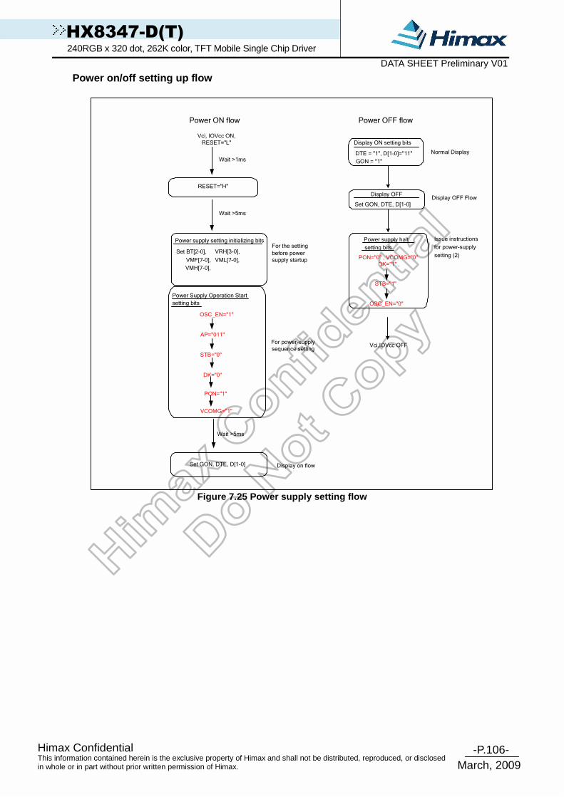
-P.106- Himax Confidential
March, 2009
This information contained herein is the exclusive property of Himax and shall not be distributed, reproduced, or disclosed in whole or in part without prior written permission of Himax.
HX8347-D(T) 240RGB x 320 dot, 262K color, TFT Mobile Single Chip Driver DATA SHEET Preliminary V01
Power on/off setting up flow
For power-supply
sequence settingSTB="0"
DK="0"
Power Supply Operation Start
setting bits
Vci, IOVcc ON,
RESET="L"
Set GON, DTE, D[1-0]
Display OFF FlowDisplay OFF
Normal DisplayDTE = "1", D[1-0]="11"
GON = "1"
Display ON setting bits
Power OFF flow
STB="1"
Issue instructions
for power-supply
setting (2)
Power supply halt
setting bits
Vci,IOVcc OFF
Set GON, DTE, D[1-0]
Power ON flow
AP="011"
OSC_EN="1"
Set BT[2-0], VRH[3-0],
VMF[7-0], VML[7-0],
VMH[7-0],
For the setting
before power
supply startup
Power supply setting initializing bits
RESET="H"
Wait >1ms
Wait >5ms
Wait >5ms
PON="0" , VCOMG="0" DK="1" ,
OSC_EN="0"
Display on flow
PON="1"
VCOMG="1"
Figure 7.25 Power supply setting flow

-P.107- Himax Confidential
March, 2009
This information contained herein is the exclusive property of Himax and shall not be distributed, reproduced, or disclosed in whole or in part without prior written permission of Himax.
HX8347-D(T) 240RGB x 320 dot, 262K color, TFT Mobile Single Chip Driver DATA SHEET Preliminary V01
7.8 Input/output pin state 7.8.1 Output pins
Output or Bi-directional pins After Power On After Hardware Reset DB17 to DB0
(Output driver) High-Z (Inactive) High-Z (Inactive)
SDA High-Z (Inactive) High-Z (Inactive) TE Low Low
CABC_PWM_OUT Low Low Table 7.23 Characteristics of output pins
7.8.2 Input pins
Input pins During Power On Process
After Power On
After Hardware Reset
During Power Off Process
NRESET Input valid Input valid Input valid Input valid NCS Input invalid Input valid Input valid Input invalid
NWR_SCL Input invalid Input valid Input valid Input invalid NRD Input invalid Input valid Input valid Input invalid
DNC_SCL Input invalid Input valid Input valid Input invalid SDA Input invalid Input valid Input valid Input invalid
VSYNC Input invalid Input valid Input valid Input invalid HSYNC Input invalid Input valid Input valid Input invalid
DE Input invalid Input valid Input valid Input invalid DOTCLK Input invalid Input valid Input valid Input invalid DB[17:0] Input invalid Input valid Input valid Input invalid
OSC, IM3,IM2, IM1,IM0, IFSEL
Input invalid Input valid Input valid Input invalid
TEST2-0 Input invalid Input valid Input valid Input invalid Table 7.24 Characteristics of input pins
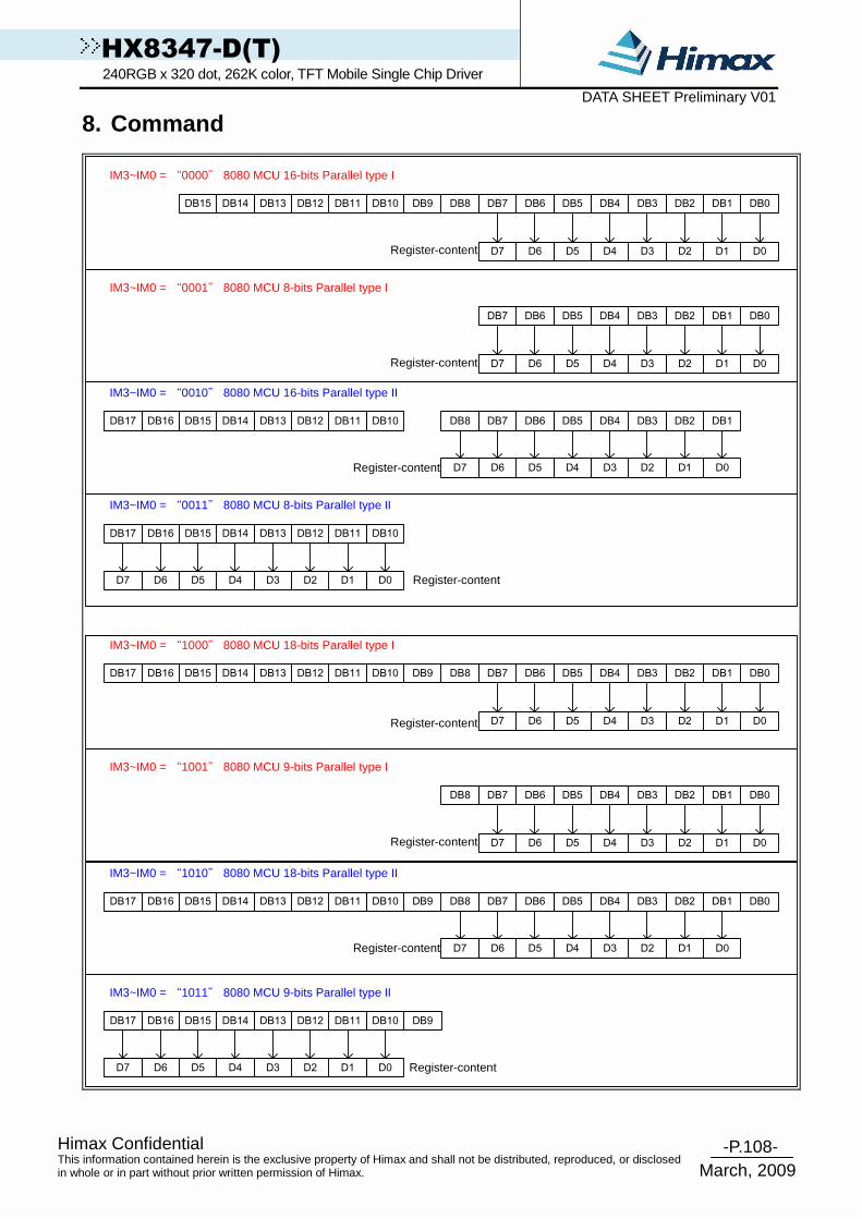
-P.108- Himax Confidential
March, 2009
This information contained herein is the exclusive property of Himax and shall not be distributed, reproduced, or disclosed in whole or in part without prior written permission of Himax.
HX8347-D(T) 240RGB x 320 dot, 262K color, TFT Mobile Single Chip Driver DATA SHEET Preliminary V01
8. Command
DB0DB1DB2DB3DB4DB5DB6DB7DB8DB9DB10DB11DB12DB13DB14DB15
D0D1D2D3D4D5D6D7
IM3~IM0 = “0000” 8080 MCU 16-bits Parallel type I
DB0DB1DB2DB3DB4DB5DB6DB7
D0D1D2D3D4D5D6D7
IM3~IM0 = “0001” 8080 MCU 8-bits Parallel type I
DB1DB2DB3DB4DB5DB6DB7DB8DB10DB11DB12DB13DB14DB15DB16DB17
D0D1D2D3D4D5D6D7
IM3~IM0 = “0010” 8080 MCU 16-bits Parallel type II
DB10DB11DB12DB13DB14DB15DB16DB17
D0D1D2D3D4D5D6D7
IM3~IM0 = “0011” 8080 MCU 8-bits Parallel type II
DB0DB1DB2DB3DB4DB5DB6DB7DB8DB9DB10DB11DB12DB13DB14DB15DB16DB17
D0D1D2D3D4D5D6D7
IM3~IM0 = “1000” 8080 MCU 18-bits Parallel type I
DB0DB1DB2DB3DB4DB5DB6DB7DB8
D0D1D2D3D4D5D6D7
IM3~IM0 = “1001” 8080 MCU 9-bits Parallel type I
DB0DB1DB2DB3DB4DB5DB6DB7DB8DB9DB10DB11DB12DB13DB14DB15DB16DB17
D0D1D2D3D4D5D6D7
IM3~IM0 = “1010” 8080 MCU 18-bits Parallel type II
DB9DB10DB11DB12DB13DB14DB15DB16DB17
D0D1D2D3D4D5D6D7
IM3~IM0 = “1011” 8080 MCU 9-bits Parallel type II
Register-content
Register-content
Register-content
Register-content
Register-content
Register-content
Register-content
Register-content

-P.109- Himax Confidential
March, 2009
This information contained herein is the exclusive property of Himax and shall not be distributed, reproduced, or disclosed in whole or in part without prior written permission of Himax.
HX8347-D(T) 240RGB x 320 dot, 262K color, TFT Mobile Single Chip Driver DATA SHEET Preliminary V01
8.1 Command set
Upper Code Lower Code
(Hex) Operation Code W/R
D[17:8] D7 D6 D5 D4 D3 D2 D1 D0 Comment
00 Himax ID R - 0 1 0 0 0 1 1 1 -
01 Display Mode control
W/R - DP_STB(0)
DP_STB_S(0)
- - SCROL (0)
IDMON (0)
INVON (0)
PTLON (0)
-
02 Column address start 2
W/R - SC[15:8] (8'b0000_0000) -
03 Column address start 1
W/R - SC[7:0] (8'b0000_0000) -
04 Column address end 2
W/R - EC[15:8] (8'b0000_0000) -
05 Column address end 1
W/R - EC[7:0] (8'b1110_1111) -
06 Row address start 2
W/R - SP[15:8] (8'b0000_0000) -
07 Row address start 1
W/R - SP[7:0] (8'b0000_00000) -
08 Row address end 2
W/R - EP[15:8] (8'b0000_0001) -
09 Row address end 1
W/R - EP[7:0] (8'b0011_1111) -
0A Partial area start row 2
W/R - PSL[15:8] (8'b0000_0000) -
0B Partial area start row 1 W/R - PSL[7:0] (8'b0000_00000) -
0C Partial area end row 2
W/R - PEL[15:8] (8'b0000_0001) -
0D Partial area end row 1 W/R - PEL[7:0] (8'b0011_1111) -
0E Vertical Scroll Top fixed area 2
W/R - TFA[15:8] (8'b0000_0000) -
0F Vertical Scroll Top fixed area 1 W/R - TFA[7:0] (8'b0000_0000) -
10 Vertical Scroll height area 2
W/R - VSA[15:8] (8'b0000_0001) -
11 Vertical Scroll height area 1 W/R - VSA[7:0] (8'b0100_0000) -
12 Vertical Scroll Button area 2
W/R - BFA[15:8] (8'b0000_0000) -
13 Vertical Scroll Button area 1 W/R - BFA [7:0] (8'b0000_0000) -
14 Vertical Scroll Start address 2
W/R - VSP [15:8] (8'b0000_0000) -
15 Vertical Scroll Start address 1 W/R - VSP [7:0] (8'b0000_0000) -
16 Memory Access control
W/R - MY(0) MX(0) MV(0) ML(0) BGR(0) - - - -
17 COLMOD W/R - CSEL[3:0] (4b’0110) - IFPF[2:0] (3b’110) -
18 OSC Control 2 W/R - I/PI_RADJ1[3:0] (3b’0011) N/P_RADJ0[3:0](4b’0100) -
19 OSC Control 1 W/R - - - - - - - - OSC_EN(0)
-
1A Power Control 1 W/R - - - - - - BT[2:0] (001) -
1B Power Control 2 W/R - - - VRH[5:0] (01_1011)_4.8V -
1C Power Control 3 W/R - - - - - - AP[2:0] (011) -
1D Power Control 4 W/R - - I/PI_FS0[2:0](100) - N/P_FS0[2:0] ](100) -
1E Power Control 5 W/R - - I/PI_FS1[2:0] ](100) - N/P_FS1[2:0] ](100) -
1F Power Control 6 W/R - GASEN(1) VCOMG(0) - PON(0) DK(1) XDK(0) DDVDH_ TRI(0) STB(1) -
22 SRAM Write Control W/R SRAM Write -
23 VCOM Control 1 W/R - VMF[7:0](1000_0000) -
24 VCOM Control 2 W/R - VMH[7:0](0111_0001) -
25 VCOM Control 3 W/R - VML[7:0](0010_1111) -
26 Display Control 1 W/R - -- - - - ISC[3:0](0001) -
27 Display Control 2 W/R - PT[1:0](10) PTV[1:0](10) - - PTG(1) REF(1) -
28 Display Control 3 W/R - - - GON(1) DTE(0) D[1:0] (00) - - -

-P.110- Himax Confidential
March, 2009
This information contained herein is the exclusive property of Himax and shall not be distributed, reproduced, or disclosed in whole or in part without prior written permission of Himax.
HX8347-D(T) 240RGB x 320 dot, 262K color, TFT Mobile Single Chip Driver DATA SHEET Preliminary V01
Upper Code Lower Code
(Hex) Operation Code W/R
D[17:8] D7 D6 D5 D4 D3 D2 D1 D0 Comment
29 Frame Rate control 1 W/R - I/PI_RTN[3:0](0010) N/P_RTN[3:0](0010) -
2A Frame Rate Control 2 W/R - - - I/PI_DIV[1:0](00) - - N/P_DIV[1:0](00) -
2B Frame Rate Control 3
W/R - N/P_DUM[7:0] (8b’0001_1100) -
2C Frame Rate Control 4 W/R - I/PI_DUM[7:0] (8b’0001_1100) -
2D Cycle Control 1 W/R - GDON[7:0] (8'b0000_1101) - 2E Cycle Control 2 W/R - GDOF[7:0] (8'b0111_0000) - 2F Display inversion W/R - - I/PI_NW[2:0](3b’001) - N/P_NW[2:0] (3b’001) -
31 RGB interface control 1 W/R - - - - - - - RCM[1:0](00) -
32 RGB interface control 2
W/R - - - - - DPL (0)
HSPL (0)
VSPL (0)
EPL (0)
-
33 RGB interface control 3 W/R - HBP[7:0] -
34 RGB interface control 4
W/R - HBP[9:8] VBP[5:0] -
36 Panel Characteristic W/R - - - - - SS_P
anel GS_Pan
el REV_Pa
nel BGR_P
anel -
38 OTP Control 1 W/R - OTP_PTM[1:0] OTP_VARDJ[1:0] OTP_POR
OTP_OTPEN
OTP_PPROG
OTP_PWE
-
39 OTP Control 2 W/R - - - - - - OTP_YA2 OTP_YA1 OTP_Y
A0 -
3A OTP Control 3 W/R - - - - OTP_XA4
OTP_XA3
OTP_XA2
OTP_XA1 OTP_XA0 -
3C CABC Control 1 W/R - DBV[7:0](8’h00) -
3D CABC Control 2 W/R - - - BCTRL (0)
- DD (0)
BL (0)
- - -
3E CABC Control 3 W/R - - - - - - - C1 (0)
C0 (0) -
3F CABC Control 4 W/R - CMB[7:0](8’h00) - 40 r1 Control (1) W/R - - - VRP0[5:0] (6’b00_0001) - 41 r1 Control (2) W/R - - - VRP1[5:0] (6’b00_1110) - 42 r1 Control (3) W/R - - - VRP2[5:0] (6’b01_0001) - 43 r1 Control (4) W/R - - - VRP3[5:0] (6’b01_1010) - 44 r1 Control (5) W/R - - - VRP4[5:0] (6’b01_1000) - 45 r1 Control (6) W/R - - - VRP5[5:0] (6’b10_0100) - 46 r1 Control (7) W/R - - PRP0[6:0] (7’b001_0101) - 47 r1 Control (8) W/R - - PRP1[6:0] (7’b110_0101) - 48 r1 Control (9) W/R - - - - PKP0[4:0] (5’b0_1011) - 49 r1 Control (10) W/R - - - - PKP1[4:0] (5’b1_100) - 4A r1 Control (11) W/R - - - - PKP2[4:0] (5’b1_1001) - 4B r1 Control (12) W/R - - - - PKP3[4:0] (5’b1_1010) - 4C r1 Control (13) W/R - - - - PKP4[4:0] (5’b1_1000) - 50 r1 Control (14) W/R - - - VRN0[5:0] (6’b01_1011) - 51 r1 Control (15) W/R - - - VRN1[5:0] (6’b10_0111) - 52 r1 Control (16) W/R - - - VRN2[5:0] (6’b10_0101) - 53 r1 Control (17) W/R - - - VRN3[5:0] (6’b10_1110) - 54 r1 Control (18) W/R - - - VRN4[5:0] (6’b11_0001) - 55 r1 Control (19) W/R - - - VRN5[5:0] (6’b11_1110) - 56 r1 Control (20) W/R - - PRN0[6:0] (7’b001_1010) - 57 r1 Control (21) W/R - - PRN1[6:0] (7’b110_1010) - 58 r1 Control (22) W/R - - - PKN0[4:0] (5’b0_0111) - 59 r1 Control (23) W/R - - - PKN1[4:0] (5’b0_0101) - 5A r1 Control (24) W/R - - - PKN2[4:0] (5’b0_0110) - 5B r1 Control (25) W/R - - - PKN3[4:0] (5’b0_1011) - 5C r1 Control (26) W/R - - - PKN4[4:0] (5’b1_0100) - 5D r1 Control (27) W/R - CGMN1[1:0] (11) CGMN0[1:0](00) CGMP1[1:0](11) CGMP0[1:0](00) -
60 TE Control W/R - - - TE_mode(0) TEOE(0) - - -
E4 Power saving 1 W/R - EQ_S1[7:0] - E5 Power saving 2 W/R - EQ_S2[7:0] - E6 Power saving 3 W/R - EQ_S3[7:0] - E7 Power saving 4 W/R - EQ_S4[7:0] -
E8 Source OP control_Normal
W/R - OPON_N[7:0] -

-P.111- Himax Confidential
March, 2009
This information contained herein is the exclusive property of Himax and shall not be distributed, reproduced, or disclosed in whole or in part without prior written permission of Himax.
HX8347-D(T) 240RGB x 320 dot, 262K color, TFT Mobile Single Chip Driver DATA SHEET Preliminary V01
Upper Code Lower Code
(Hex) Operation Code W/R
D[17:8] D7 D6 D5 D4 D3 D2 D1 D0 Comment
E9 Source OP control_IDLE W/R - OPON_I[7:0] -
EA Power control internal use (1) W/R - STBA[15:8] -
EB Power control internal use (2)
W/R - STBA[7:0] -
EC Source control internal use (1) W/R - PTBA[15:8] -
ED Source control internal use (2)
W/R - PTBA[7:0] -
FF Page select W/R - - - - - - - PAGE_SEL[1:0] (00) -
Table 8.1 List table of command set page 0

-P.112- Himax Confidential
March, 2009
This information contained herein is the exclusive property of Himax and shall not be distributed, reproduced, or disclosed in whole or in part without prior written permission of Himax.
HX8347-D(T) 240RGB x 320 dot, 262K color, TFT Mobile Single Chip Driver DATA SHEET Preliminary V01
Upper Code Lower Code
(Hex) Operation Code W/R
D[17:8] D7 D6 D5 D4 D3 D2 D1 D0 Comment
C3 CABC Control 5 W/R - 0 PWMDIV[2:0](000) 1 1 INPLUS (1) 1 -
C5 CABC Control 6 W/R - PWM_PERIOD[7:0] (43d) - C7 CABC Control 7 W/R - - DIM_FRAME[6:0] (20) -
CB Gain select register 0
W/R - - DBG0[6:0](40) -
CC Gain select register 1 W/R - - DBG1[6:0](3C) -
CD Gain select register 2 W/R - - DBG2[6:0](38) -
CE Gain select register 3 W/R - - DBG3[6:0](34) -
CF Gain select register 4 W/R - - DBG4[6:0](33) -
D0 Gain select register 5 W/R - - DBG5[6:0](32) -
D1 Gain select register 6 W/R - - DBG6[6:0](2B) -
D2 Gain select register 7 W/R - - DBG7[6:0](24) -
D3 Gain select register 8 W/R - - DBG8[6:0](22) -
FF Page select W/R - - - - - - - PAGE_SEL[1:0] (00) -
Table 8.2 List table of command set page 1

-P.113- Himax Confidential
March, 2009
This information contained herein is the exclusive property of Himax and shall not be distributed, reproduced, or disclosed in whole or in part without prior written permission of Himax.
HX8347-D(T) 240RGB x 320 dot, 262K color, TFT Mobile Single Chip Driver DATA SHEET Preliminary V01
8.2 Index register
RB7
W
R/W
0
DNC
ID7 ID6 ID5 ID4 ID3 ID2 ID1 ID0
RB6 RB5 RB4 RB3 RB2 RB1 RB0
R 0 ID7 ID6 ID5 ID4 ID3 ID2 ID1 ID0
Figure 8.1 Index register
Index register (IR) specifies the Index of register from R00h to RFFh. It sets the register number (ID7-0) in the range from 00000000b to 11111111b in binary form.
8.3 Himax ID register (PAGE0 - R00h)
RB7RRRR////WWWW DNCDNCDNCDNC RB6 RB5 RB4 RB3 RB2 RB1 RB0
RRRR 1111 0 1 0 0 0 1 1 1
Figure 8.2 Himax ID register (PAGE0 -00h)
This command is used to read this IC’s ID code. The ID code of this IC is 47h.
8.4 Display mode control register (PAGE0 -01h)
RB7
WWWW
RRRR////WWWW
1111
DNCDNCDNCDNC
DP_STB
DP_STB_S
SCROLL
IDMON
INVON
PLTON
RB6 RB5 RB4 RB3 RB2 RB1 RB0
*
RRRR 1111
*
DP_
STBDP_S
TB_S0 0
SCR
OLLIDMO
N
INVO
N
PLT
ON
Figure 8.3 Display mode control register (PAGE0 -01 h)
DP_STB, DP_STB_S : These two bits can let the driver into the deep standby mode. And when into deep standby, all display operation stops, including the internal R-C oscillator. In the deep standby mode, the GRAM data and register content are not retained. For details, please refer to “7.7 Power On/Off Sequence” section for detail use. IDMON: This bit is Idle mode (8-color display mode) enable bit. IDMON = ‘1’, chip will be into idle mode, and color expression is reduced. The primary and the secondary colors using MSB of each R, G and B in the Frame Memory, 8 color depth data is displayed.
Display(Idel Mode On Example)
Memory
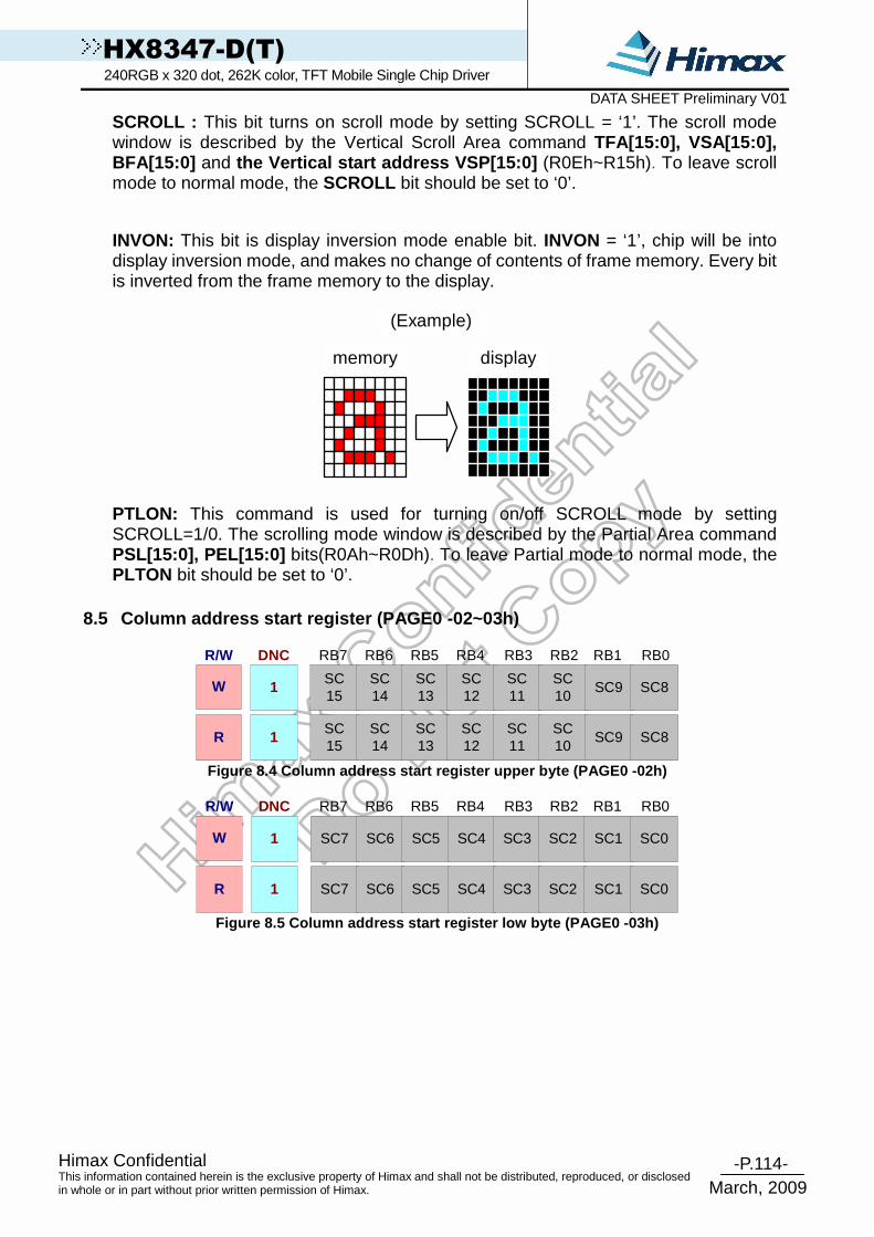
-P.114- Himax Confidential
March, 2009
This information contained herein is the exclusive property of Himax and shall not be distributed, reproduced, or disclosed in whole or in part without prior written permission of Himax.
HX8347-D(T) 240RGB x 320 dot, 262K color, TFT Mobile Single Chip Driver DATA SHEET Preliminary V01
SCROLL : This bit turns on scroll mode by setting SCROLL = ‘1’. The scroll mode window is described by the Vertical Scroll Area command TFA[15:0], VSA[15:0], BFA[15:0] and the Vertical start address VSP[15:0] (R0Eh~R15h). To leave scroll mode to normal mode, the SCROLL bit should be set to ‘0’.
INVON: This bit is display inversion mode enable bit. INVON = ‘1’, chip will be into display inversion mode, and makes no change of contents of frame memory. Every bit is inverted from the frame memory to the display.
memory display
(Example)
PTLON: This command is used for turning on/off SCROLL mode by setting SCROLL=1/0. The scrolling mode window is described by the Partial Area command PSL[15:0], PEL[15:0] bits(R0Ah~R0Dh). To leave Partial mode to normal mode, the PLTON bit should be set to ‘0’.
8.5 Column address start register (PAGE0 -02~03h)
RB7
W
R/W
1
DNC
SC15
SC14
SC13
SC12
SC11
SC10
SC9 SC8
RB6 RB5 RB4 RB3 RB2 RB1 RB0
R 1SC15
SC14
SC13
SC12
SC11
SC10
SC9 SC8
Figure 8.4 Column address start register upper byte (PAGE0 -02h)
RB7
W
R/W
1
DNC
SC7 SC6 SC5 SC4 SC3 SC2 SC1 SC0
RB6 RB5 RB4 RB3 RB2 RB1 RB0
R 1 SC7 SC6 SC5 SC4 SC3 SC2 SC1 SC0
Figure 8.5 Column address start register low byte ( PAGE0 -03h)

-P.115- Himax Confidential
March, 2009
This information contained herein is the exclusive property of Himax and shall not be distributed, reproduced, or disclosed in whole or in part without prior written permission of Himax.
HX8347-D(T) 240RGB x 320 dot, 262K color, TFT Mobile Single Chip Driver DATA SHEET Preliminary V01
8.6 Column address end register (PAGE0 -04~05h)
RB7
W
R/W
1
DNC
EC15
EC14
EC13
EC12
EC11
EC10
EC9 EC8
RB6 RB5 RB4 RB3 RB2 RB1 RB0
R 1EC15
EC14
EC13
EC12
EC11
EC10
EC9 EC8
Figure 8.6 Column address end register upper byte ( PAGE0 -04h)
RB7
W
R/W
1
DNC
EC7 EC6 EC5 EC4 EC3 EC2 EC1 EC0
RB6 RB5 RB4 RB3 RB2 RB1 RB0
R 1 EC7 EC6 EC5 EC4 EC3 EC2 EC1 EC0
Figure 8.7 Column address end register low byte (PA GE0 -05h) 8.7 Row address start register (PAGE0 -06~07h)
RB7
W
R/W
1
DNC
SP15
SP14
SP13
SP12
SP11
SP10
SP9 SP8
RB6 RB5 RB4 RB3 RB2 RB1 RB0
R 1SP15
SP14
SP13
SP12
SP11
SP10
SP9 SP8
Figure 8.8 Row address start register upper byte (P AGE0 -06h)
RB7
W
R/W
1
DNC
SP7 SP6 SP5 SP4 SP3 SP2 SP1 SP0
RB6 RB5 RB4 RB3 RB2 RB1 RB0
R 1 SP7 SP6 SP5 SP4 SP3 SP2 SP1 SP0
Figure 8.9 Row address start register low byte (PAG E0 -07h) 8.8 Row address end register (PAGE0 -08~09h)
RB7
W
R/W
1
DNC
EP15
EP14
EP13
EP12
EP11
EP10
EP9 EP8
RB6 RB5 RB4 RB3 RB2 RB1 RB0
R 1EP15
EP14
EP13
EP12
EP11
EP10
EP9 EP8
Figure 8.10 Row address end register upper byte (PA GE0 -08h)
RB7
W
R/W
1
DNC
EP7 EP6 EP5 EP4 EP3 EP2 EP1 EP0
RB6 RB5 RB4 RB3 RB2 RB1 RB0
R 1 EP7 EP6 EP5 EP4 EP3 EP2 EP1 EP0
Figure 8.11 Row address end register low byte (PAGE 0 -09h)
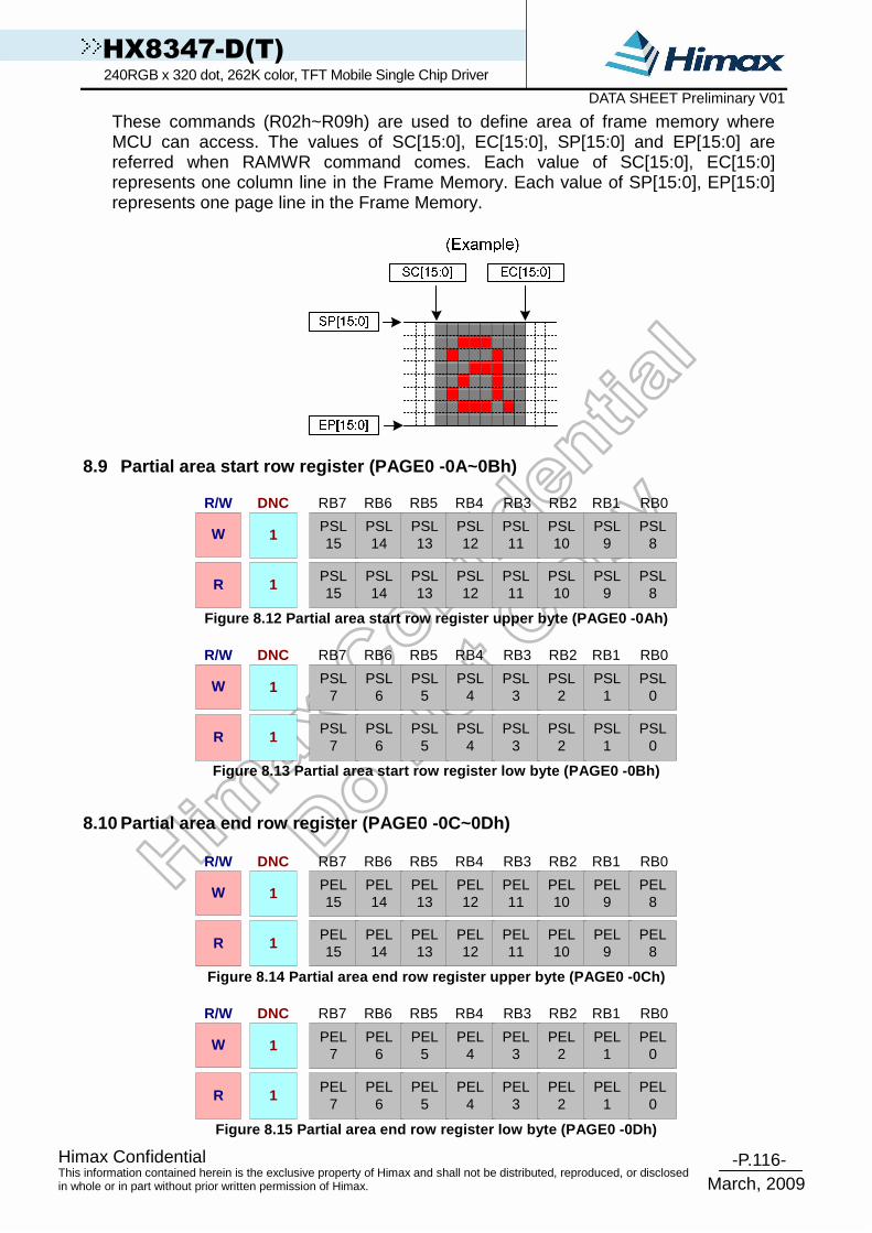
-P.116- Himax Confidential
March, 2009
This information contained herein is the exclusive property of Himax and shall not be distributed, reproduced, or disclosed in whole or in part without prior written permission of Himax.
HX8347-D(T) 240RGB x 320 dot, 262K color, TFT Mobile Single Chip Driver DATA SHEET Preliminary V01
These commands (R02h~R09h) are used to define area of frame memory where MCU can access. The values of SC[15:0], EC[15:0], SP[15:0] and EP[15:0] are referred when RAMWR command comes. Each value of SC[15:0], EC[15:0] represents one column line in the Frame Memory. Each value of SP[15:0], EP[15:0] represents one page line in the Frame Memory.
8.9 Partial area start row register (PAGE0 -0A~0Bh)
RB7
W
R/W
1
DNC
PSL15
PSL14
PSL13
PSL12
PSL11
PSL10
PSL9
PSL8
RB6 RB5 RB4 RB3 RB2 RB1 RB0
R 1PSL15
PSL14
PSL13
PSL12
PSL11
PSL10
PSL9
PSL8
Figure 8.12 Partial area start row register upper b yte (PAGE0 -0Ah)
RB7
W
R/W
1
DNC
PSL7
PSL6
PSL5
PSL4
PSL3
PSL2
PSL1
PSL0
RB6 RB5 RB4 RB3 RB2 RB1 RB0
R 1PSL
7PSL
6PSL
5PSL
4PSL
3PSL
2PSL
1PSL
0
Figure 8.13 Partial area start row register low byt e (PAGE0 -0Bh)
8.10 Partial area end row register (PAGE0 -0C~0Dh)
RB7
W
R/W
1
DNC
PEL15
PEL14
PEL13
PEL12
PEL11
PEL10
PEL9
PEL8
RB6 RB5 RB4 RB3 RB2 RB1 RB0
R 1PEL15
PEL14
PEL13
PEL12
PEL11
PEL10
PEL9
PEL8
Figure 8.14 Partial area end row register upper byt e (PAGE0 -0Ch)
RB7
W
R/W
1
DNC
PEL7
PEL6
PEL5
PEL4
PEL3
PEL2
PEL1
PEL0
RB6 RB5 RB4 RB3 RB2 RB1 RB0
R 1PEL
7PEL
6PEL
5PEL
4PEL
3PEL
2PEL
1PEL
0
Figure 8.15 Partial area end row register low byte (PAGE0 -0Dh)

-P.117- Himax Confidential
March, 2009
This information contained herein is the exclusive property of Himax and shall not be distributed, reproduced, or disclosed in whole or in part without prior written permission of Himax.
HX8347-D(T) 240RGB x 320 dot, 262K color, TFT Mobile Single Chip Driver DATA SHEET Preliminary V01
These commands (PAGE0 -0Ah~~0Dh) define the partial mode’s display area. The Start Row (PSL) and the second the End Row (PEL) are illustrated in the figures below. PSL and PEL refer to the Frame Memory Line Pointer. If End Row > Start Row
PSL [15:0]
PEL[15:0]
Start Row
End Row
Partial Display Area
If End Row < Start Row
If End Row = Start Row then the Partial Area will be one row deep.
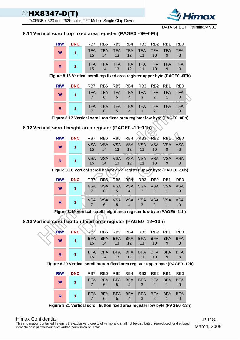
-P.118- Himax Confidential
March, 2009
This information contained herein is the exclusive property of Himax and shall not be distributed, reproduced, or disclosed in whole or in part without prior written permission of Himax.
HX8347-D(T) 240RGB x 320 dot, 262K color, TFT Mobile Single Chip Driver DATA SHEET Preliminary V01
8.11 Vertical scroll top fixed area register (PAGE0 -0E~0Fh)
RB7
W
R/W
1
DNC
TFA15
TFA14
TFA13
TFA12
TFA11
TFA10
TFA9
TFA8
RB6 RB5 RB4 RB3 RB2 RB1 RB0
R 1TFA15
TFA14
TFA13
TFA12
TFA11
TFA10
TFA9
TFA8
Figure 8.16 Vertical scroll top fixed area register upper byte (PAGE0 -0Eh)
RB7
W
R/W
1
DNC
TFA7
TFA6
TFA5
TFA4
TFA3
TFA2
TFA1
TFA0
RB6 RB5 RB4 RB3 RB2 RB1 RB0
R 1TFA
7TFA
6TFA
5TFA
4TFA
3TFA
2TFA
1TFA
0
Figure 8.17 Vertical scroll top fixed area register low byte (PAGE0 -0Fh) 8.12 Vertical scroll height area register (PAGE0 -1 0~11h)
RB7
W
R/W
1
DNC
VSA15
VSA14
VSA13
VSA12
VSA11
VSA10
VSA9
VSA8
RB6 RB5 RB4 RB3 RB2 RB1 RB0
R 1VSA15
VSA14
VSA13
VSA12
VSA11
VSA10
VSA9
VSA8
Figure 8.18 Vertical scroll height area register up per byte (PAGE0 -10h)
RB7
W
R/W
1
DNC
VSA7
VSA6
VSA5
VSA4
VSA3
VSA2
VSA1
VSA0
RB6 RB5 RB4 RB3 RB2 RB1 RB0
R 1VSA
7VSA
6VSA
5VSA
4VSA
3VSA
2VSA
1VSA
0
Figure 8.19 Vertical scroll height area register lo w byte (PAGE0 -11h)
8.13 Vertical scroll button fixed area register (PA GE0 -12~13h)
RB7
W
R/W
1
DNC
BFA15
BFA14
BFA13
BFA12
BFA11
BFA10
BFA9
BFA8
RB6 RB5 RB4 RB3 RB2 RB1 RB0
R 1BFA15
BFA14
BFA13
BFA12
BFA11
BFA10
BFA9
BFA8
Figure 8.20 Vertical scroll button fixed area regis ter upper byte (PAGE0 -12h)
RB7
W
R/W
1
DNC
BFA7
BFA6
BFA5
BFA4
BFA3
BFA2
BFA1
BFA0
RB6 RB5 RB4 RB3 RB2 RB1 RB0
R 1BFA
7BFA
6BFA
5BFA
4BFA
3BFA
2BFA
1BFA
0
Figure 8.21 Vertical scroll button fixed area regis ter low byte (PAGE0 -13h)

-P.119- Himax Confidential
March, 2009
This information contained herein is the exclusive property of Himax and shall not be distributed, reproduced, or disclosed in whole or in part without prior written permission of Himax.
HX8347-D(T) 240RGB x 320 dot, 262K color, TFT Mobile Single Chip Driver DATA SHEET Preliminary V01
These commands (PAGE0 -0E~0Fh, R10~11h, R12~13h) define the Vertical Scrolling Area of the display. TFA[15:0] describes the Top Fixed Area (in No. of lines from Top of the Frame Memory and Display). VSA[15:0] describes the height of the Vertical Scrolling Area (in No. of lines of the Frame Memory [not the display] from the Vertical Scrolling Start Address). The first line read from Frame Memory appears immediately after the bottom most line of the Top Fixed Area. BFA[15:0] describes the Bottom Fixed Area (in No. of lines from Bottom of the Frame Memory and Display). TFA, VSA and BFA refer to the Frame Memory Line Pointer.
Please note that (TFA+VSA+BFA) must be set to ‘320d’, otherwise Scrolling mode is undefined. In Vertical Scroll Mode, MV bit should be set to ‘0’ – this only affects the Frame Memory Write.

-P.120- Himax Confidential
March, 2009
This information contained herein is the exclusive property of Himax and shall not be distributed, reproduced, or disclosed in whole or in part without prior written permission of Himax.
HX8347-D(T) 240RGB x 320 dot, 262K color, TFT Mobile Single Chip Driver DATA SHEET Preliminary V01
8.14 Vertical scroll start address register (PAGE0 -14~15h)
RB7
W
R/W
1
DNC
VSP15
VSP14
VSP13
VSP12
VSP11
VSP10
VSP9
VSP8
RB6 RB5 RB4 RB3 RB2 RB1 RB0
R 1VSP15
VSP14
VSP13
VSP12
VSP11
VSP10
VSP9
VSP8
Figure 8.22 Vertical scroll start address register upper byte (PAGE0 -14h)
RB7
W
R/W
1
DNC
VSP7
VSP6
VSP5
VSP4
VSP3
VSP2
VSP1
VSP0
RB6 RB5 RB4 RB3 RB2 RB1 RB0
R 1VSP
7VSP
6VSP
5VSP
4VSP
3VSP
2VSP
1VSP
0
Figure 8.23 Vertical scroll start address register low byte (PAGE0 -15h)
VSP[15:0] is used together with Vertical Scrolling Definition register (PAGE0 -0Eh~R13h), which describe the scrolling area and the scrolling mode. VSP[15:0] refers to the Frame Memory line Pointer, and describes the address of the line in the Frame Memory that will be written as the first line after the last line of the Top Fixed Area on the display as illustrated below: Example: When Top Fixed Area TFA = ‘00d’, Bottom Fixed Area BFA = ‘02’d, Vertical Scrolling Area VSA = ‘318'd’ and VSP = ‘3d’ (SMX = ‘L’, SMY = ‘L’)
Memory(0,0)
0123:::
Line Pointer
318319
DisplayPointer
VSP[15:0]
(0,319)
:
(Example)
When new Pointer position and Picture Data are sent, the result on the display will happen at the next Panel Scan to avoid tearing effect.
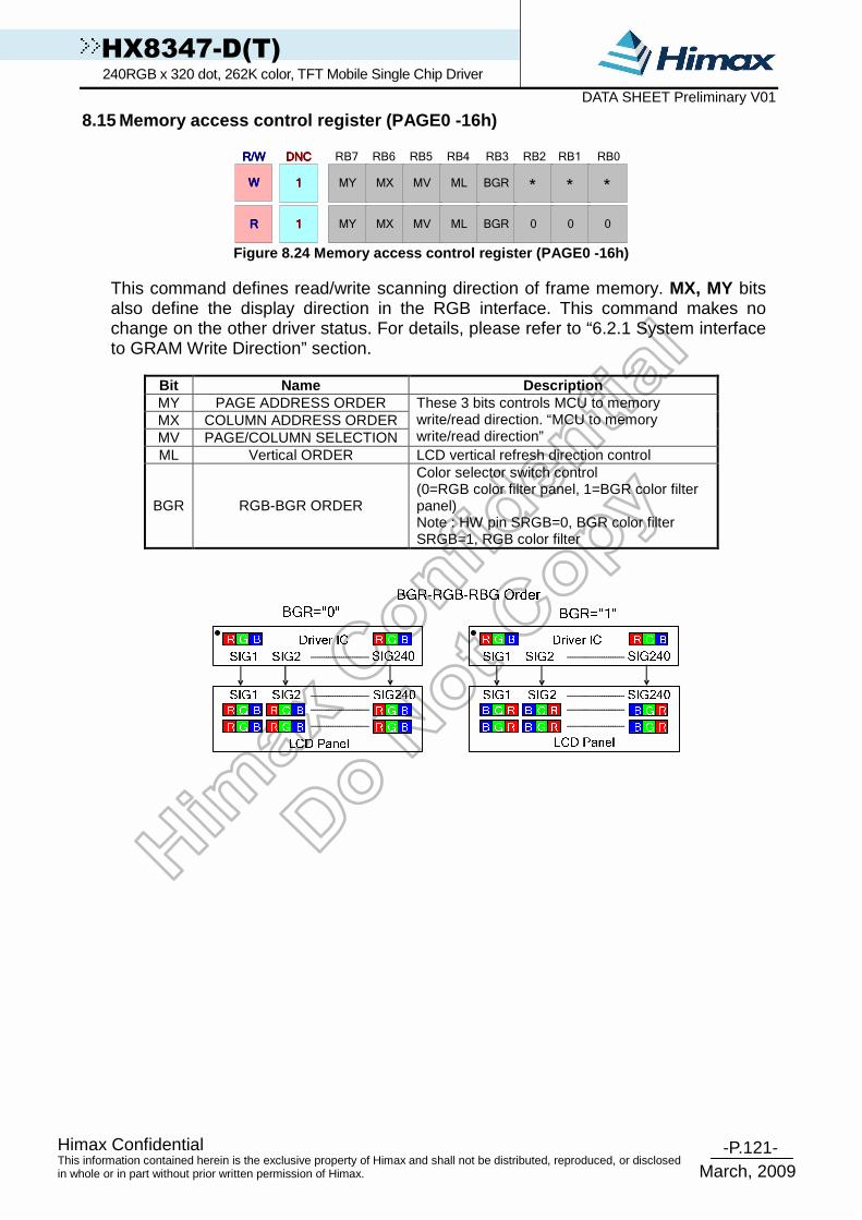
-P.121- Himax Confidential
March, 2009
This information contained herein is the exclusive property of Himax and shall not be distributed, reproduced, or disclosed in whole or in part without prior written permission of Himax.
HX8347-D(T) 240RGB x 320 dot, 262K color, TFT Mobile Single Chip Driver DATA SHEET Preliminary V01
8.15 Memory access control register (PAGE0 -16h)
RB7
WWWW
RRRR////WWWW
1111
DNCDNCDNCDNC
MY MX MV ML BGR
RB6 RB5 RB4 RB3 RB2 RB1 RB0
* *
RRRR 1111
*
MY MX MV ML BGR 0 0 0
Figure 8.24 Memory access control register (PAGE0 - 16h)
This command defines read/write scanning direction of frame memory. MX, MY bits also define the display direction in the RGB interface. This command makes no change on the other driver status. For details, please refer to “6.2.1 System interface to GRAM Write Direction” section.
Bit Name Description MY PAGE ADDRESS ORDER MX COLUMN ADDRESS ORDER MV PAGE/COLUMN SELECTION
These 3 bits controls MCU to memory write/read direction. “MCU to memory write/read direction”
ML Vertical ORDER LCD vertical refresh direction control
BGR RGB-BGR ORDER
Color selector switch control (0=RGB color filter panel, 1=BGR color filter panel) Note : HW pin SRGB=0, BGR color filter SRGB=1, RGB color filter

-P.122- Himax Confidential
March, 2009
This information contained herein is the exclusive property of Himax and shall not be distributed, reproduced, or disclosed in whole or in part without prior written permission of Himax.
HX8347-D(T) 240RGB x 320 dot, 262K color, TFT Mobile Single Chip Driver DATA SHEET Preliminary V01
8.16 COLMOD control register (PAGE0 -17h)
RB7
WWWW
RRRR////WWWW
1111
DNCDNCDNCDNC RB6 RB5 RB4 RB3 RB2 RB1 RB0
RRRR 1111
CSEL3 CSEL2 CSEL1 CSEL0 * IFPF2 IFPF1 IFPF0
CSEL3 CSEL2 CSEL1 CSEL0 * IFPF2 IFPF1 IFPF0
Figure 8.25 COLMOD control register (PAGE0 -17h)
This command is used to define the format of RGB picture data, which is to be transfer via the system and RGB interface. The formats are shown in the table: System interface
Interface Format IFPF2 IFPF1 IFPF0 Not Defined 0 0 0 Not Defined 0 0 1 Not Defined 0 1 0 12 Bit/Pixel 0 1 1 Not Defined 1 0 0 16 Bit/Pixel 1 0 1 18 Bit/Pixel 1 1 0 18 Bit/Pixel at 16-bits data bus interface (16+2)
1 1 1
RGB interface
Interface Format CSEL3 CSEL2 CSEL1 CSEL0 16 Bit/Pixel 0 1 0 1 18 Bit/Pixel 0 1 1 0 6 Bit/Pixel 1 1 1 0 Not Defined The Other Setting

-P.123- Himax Confidential
March, 2009
This information contained herein is the exclusive property of Himax and shall not be distributed, reproduced, or disclosed in whole or in part without prior written permission of Himax.
HX8347-D(T) 240RGB x 320 dot, 262K color, TFT Mobile Single Chip Driver DATA SHEET Preliminary V01
8.17 OSC control register (PAGE0 -18h & R19h)
RB7
WWWW
RRRR////WWWW
1111
DNCDNCDNCDNC
I/P_R
ADJ3
I/P_R
ADJ2
IP_RA
DJ1
N/P_R
ADJ3
N/P_R
ADJ2
N/P_R
ADJ1
N/P_R
ADJ0
RB6 RB5 RB4 RB3 RB2 RB1 RB0
RRRR 1111
I/P_R
ADJ0
I/P_R
ADJ3
I/P_R
ADJ2
IP_RA
DJ1
N/P_R
ADJ3
N/P_R
ADJ2
N/P_R
ADJ1
N/P_R
ADJ0
I/P_R
ADJ0
Figure 8.26 OSC control 1 register (PAGE0 -18h)
RB7
WWWW
RRRR////WWWW
1111
DNCDNCDNCDNC
OSC_
EN
RB6 RB5 RB4 RB3 RB2 RB1 RB0
*** *
RRRR 1111
* *
0 0 0 0 0 0 0OSC_
EN
*
Figure 8.27 OSC control 2 register (PAGE0 -19h)
These commands are used to set internal oscillator related setting OSC_EN: Enable internal oscillator, OSC_EN = ‘1’, internal oscillator start to oscillate. OSC_EN = ‘0’, internal oscillator stop. In RGB interface mode (PAGE0 -CM[1:0] = ‘10’ or ‘11’), internal oscillator will be stop to oscillate and OSC_EN bit control is invalid. N/P_RADJ[2:0]: Internal oscillator frequency adjusts in Normal / Partial mode. I/PI_RADJ[2:0]: Internal oscillator frequency adjusts in Idle(8-color) / Partial Idle mode. For details, please refer to “7.1 Internal Oscillator” section.
RADJ3 RADJ2 RADJ1 RADJ0 Internal Oscillator Frequency
Display Frame rate
0 0 0 0 50% x 2.85MHz 35Hz 0 0 0 1 67% x 2.85MHz 45Hz 0 0 1 0 75% x 2.85MHz 50Hz 0 0 1 1 83% x 2.85MHz 55Hz 0 1 0 0 100% x2.85MHz 65Hz 0 1 0 1 108% x 2.85MHz 70Hz 0 1 1 0 117% x 2.85MHz 75Hz 0 1 1 1 125% x 2.85MHz 80Hz 1 0 0 0 100% x 2.85MHz 65Hz 1 0 0 1 133% x 2.85MHz 90Hz 1 0 1 0 150% x 2.85MHz 100Hz 1 0 1 1 167% x 2.85MHz 110Hz 1 1 0 0 200% x 2.85MHz 130Hz 1 1 0 1 217% x 2.85MHz 140Hz 1 1 1 0 233% x 2.85MHz 150Hz 1 1 1 1 250% x 2.85MHz 160Hz

-P.124- Himax Confidential
March, 2009
This information contained herein is the exclusive property of Himax and shall not be distributed, reproduced, or disclosed in whole or in part without prior written permission of Himax.
HX8347-D(T) 240RGB x 320 dot, 262K color, TFT Mobile Single Chip Driver DATA SHEET Preliminary V01
8.18 Power control 1 register (PAGE0 -1Ah)
RB7
WWWW
RRRR////WWWW
1111
DNCDNCDNCDNC
* * * * * BT2 BT1 BT0
RB6 RB5 RB4 RB3 RB2 RB1 RB0
RRRR 1111 * * * * * BT2 BT0 BT0
Figure 8.28 Power control 1 register (PAGE0 -1Ah)
BT[2:0]: Switch the output factor of step-up circuit 2 for VGH and VGL voltage generation. The LCD drive voltage level can be selected according to the characteristic of liquid crystal which panel used. Lower amplification of the step-up circuit consumes less current and then the power consumption can be reduced.
BT2 BT1 BT0 DDVDH VCL VGH VGL
0 0 0 5.0V -VCI 3DDVDH -VCI-2DDVDH 0 0 1 5.0V -VCI 3DDVDH -2DDVDH 0 1 0 5.0V -VCI 3DDVDH VCI-2DDVDH 0 1 1 5.0V -VCI VCI+2DDVDH -VCI-2DDVDH 1 0 0 5.0V -VCI VCI+2DDVDH -2DDVDH 1 0 1 5.0V -VCI VCI+2DDVDH VCI-2DDVDH 1 1 0 5.0V -VCI 2DDVDH -2DDVDH 1 1 1 5.0V -VCI 2DDVDH -VCI-DDVDH
Note: When VCI = 2.8V, DDVDH_TRI=0
BT2 BT1 BT0 DDVDH VCL VGH VGL
0 0 0 6.1V -VCI Setting
inhabited Setting
inhabited 0 0 1 6.1V -VCI 3DDVDH -2DDVDH 0 1 0 6.1V -VCI 3DDVDH VCI-2DDVDH 0 1 1 6.1V -VCI VCI+2DDVDH -VCI-2DDVDH 1 0 0 6.1V -VCI VCI+2DDVDH -2DDVDH 1 0 1 6.1V -VCI VCI+2DDVDH VCI-2DDVDH 1 1 0 6.1V -VCI 2DDVDH -2DDVDH 1 1 1 6.1V -VCI 2DDVDH -VCI-DDVDH
Note: When VCI = 2.8V, DDVDH_TRI=1

-P.125- Himax Confidential
March, 2009
This information contained herein is the exclusive property of Himax and shall not be distributed, reproduced, or disclosed in whole or in part without prior written permission of Himax.
HX8347-D(T) 240RGB x 320 dot, 262K color, TFT Mobile Single Chip Driver DATA SHEET Preliminary V01
8.19 Power control 2 register (PAGE0 -1Bh)
RB7
WWWW
RRRR////WWWW
1111
DNCDNCDNCDNC
* * VRH5 VRH4 VRH3 VRH2 VRH1 VRH0
RB6 RB5 RB4 RB3 RB2 RB1 RB0
RRRR 1111 * * VRH5 VRH4 VRH3 VRH2 VRH1 VRH0
Figure 8.29 Power control 2 register (PAGE0 -1Bh)
VRH[4:0]: Specify the VREG1 voltage adjusting. VREG1 voltage is for gamma voltage setting.VREG1=Decimal(VRH[5:0])x0.05+3.3.
VRH5 VRH4 VRH3 VRH2 VRH1 VRH0 VREG1 (DDVDH_TRI=0)
VREG1 (DDVDH_TRI=1)
0 0 0 0 0 0 3.30 3.30 0 0 0 0 0 1 3.35 3.35 0 0 0 0 1 0 3.40 3.40 0 0 0 0 1 1 3.45 3.45 0 0 0 1 0 0 3.50 3.50 0 0 0 1 0 1 3.55 3.55 0 0 0 1 1 0 3.60 3.60 0 0 0 1 1 1 3.65 3.65 0 0 1 0 0 0 3.70 3.70 : : : : : : : : 0 1 1 1 0 1 4.75 4.75 0 1 1 1 1 0 4.80 4.80 0 1 1 1 1 1 STOP 4.85 1 0 0 0 0 0 STOP 4.90 1 0 0 0 0 1 STOP 4.95 : : : : : : : : 1 1 0 0 0 0 STOP 5.70 1 1 0 0 0 1 STOP 5.75 1 1 0 0 1 0 STOP 5.80 1 1 0 0 1 1 STOP STOP 1 1 1 0 1 1 STOP STOP : : : : : : : : 1 1 1 1 1 0 STOP STOP
1 1 1 1 1 1 Internal circuit operations stop. The gamma voltage can be adjusted from external VREG1 input.
Note: Internal VREF can be modified by Custom’s special request. default VREF=4.8 if DDVDH_TRI=0 and VREF=5.8 if DDVDH_TRI=1 VREG1=Decimal(VRH[5:0])x0.05+3.3 *(VREF/4.8) if DDVDH_TRI=0. VREG1=Decimal(VRH[5:0])x0.05+3.3 *(VREF/5.8) if DDVDH_TRI=1.
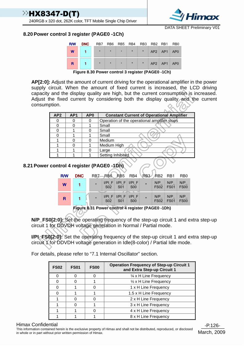
-P.126- Himax Confidential
March, 2009
This information contained herein is the exclusive property of Himax and shall not be distributed, reproduced, or disclosed in whole or in part without prior written permission of Himax.
HX8347-D(T) 240RGB x 320 dot, 262K color, TFT Mobile Single Chip Driver DATA SHEET Preliminary V01
8.20 Power control 3 register (PAGE0 -1Ch)
RB7
WWWW
RRRR////WWWW
1111
DNCDNCDNCDNC
* * * * * AP2 AP1 AP0
RB6 RB5 RB4 RB3 RB2 RB1 RB0
RRRR 1111 * * * * * AP2 AP1 AP0
Figure 8.30 Power control 3 register (PAGE0 -1Ch)
AP[2:0]: Adjust the amount of current driving for the operational amplifier in the power supply circuit. When the amount of fixed current is increased, the LCD driving capacity and the display quality are high, but the current consumption is increased. Adjust the fixed current by considering both the display quality and the current consumption.
AP2 AP1 AP0 Constant Current of Operational Amplifier
0 0 0 Operation of the operational amplifier stops 0 0 1 Small 0 1 0 Small 0 1 1 Small 1 0 0 Medium 1 0 1 Medium High 1 1 0 Large 1 1 1 Setting Inhibited
8.21 Power control 4 register (PAGE0 -1Dh)
RB7
WWWW
RRRR////WWWW
1111
DNCDNCDNCDNC
*I/PI_F
S02
I/PI_F
S01
I/PI_F
S00*
N/P_
FS02
N/P_
FS01
N/P_
FS00
RB6 RB5 RB4 RB3 RB2 RB1 RB0
RRRR 1111 *I/PI_F
S02
I/PI_F
S01
I/PI_F
S00*
N/P_
FS02
N/P_
FS01
N/P_
FS00
Figure 8.31 Power control 4 register (PAGE0 -1Dh)
N/P_FS0[2:0]: Set the operating frequency of the step-up circuit 1 and extra step-up circuit 1 for DDVDH voltage generation in Normal / Partial mode. I/PI_FS0[2:0]: Set the operating frequency of the step-up circuit 1 and extra step-up circuit 1 for DDVDH voltage generation in Idle(8-color) / Partial Idle mode. For details, please refer to “7.1 Internal Oscillator” section.
FS02 FS01 FS00 Operation Frequency of Step-up Circuit 1 and Extra Step-up Circuit 1
0 0 0 ¼ x H Line Frequency 0 0 1 ½ x H Line Frequency 0 1 0 1 x H Line Frequency 0 1 1 1.5 x H Line Frequency 1 0 0 2 x H Line Frequency 1 0 1 3 x H Line Frequency 1 1 0 4 x H Line Frequency 1 1 1 8 x H Line Frequency

-P.127- Himax Confidential
March, 2009
This information contained herein is the exclusive property of Himax and shall not be distributed, reproduced, or disclosed in whole or in part without prior written permission of Himax.
HX8347-D(T) 240RGB x 320 dot, 262K color, TFT Mobile Single Chip Driver DATA SHEET Preliminary V01
8.22 Power control 5 register (PAGE0 -1Eh)
RB7
WWWW
RRRR////WWWW
1111
DNCDNCDNCDNC
*I/PI_F
S12
I/PI_F
S11
I/PI_F
S10*
N/P_
FS12
N/P_
FS11
N/P_
FS10
RB6 RB5 RB4 RB3 RB2 RB1 RB0
RRRR 1111 *I/PI_F
S12
I/PI_F
S11
I/PI_F
S10*
N/P_
FS12
N/P_
FS11
N/P_
FS10
Figure 8.32 Power control 5 register (PAGE0 -1Eh)
N/P_FS1[2:0]: Set the operating frequency of the step-up circuit 2 and 3 for VGH, VGL and VCL voltage generation in Normal / Partial mode. I/PI_FS1[2:0]: Set the operating frequency of the step-up circuit 2 and 3 for VGH, VGL and VCL voltage generation in Idle(8-color) / Partial Idle mode. For details, please refer to “7.1 Internal Oscillator” section.
FS12 FS11 FS10 Operation Frequency of Step-up Circuit 2 , Step-up Circuit 3
0 0 0 ¼ x H Line Frequency 0 0 1 ½ x H Line Frequency 0 1 0 1 x H Line Frequency 0 1 1 1.5 x H Line Frequency 1 0 0 2 x H Line Frequency 1 0 1 3 x H Line Frequency 1 1 0 4 x H Line Frequency 1 1 1 8 x H Line Frequency
Note: Ensure that the operation frequency of step-up circuit 1 ≧ step-up circuit 2 8.23 Power control 6 register (PAGE0 -1Fh)
RB7
WWWW
RRRR////WWWW
1111
DNCDNCDNCDNC
GAS
EN
VCO
MG* PON DK XDK
DDVDH_T
RISTB
RB6 RB5 RB4 RB3 RB2 RB1 RB0
RRRR 1111GASEN
VCOMG
* PON DK XDKDDV
DH_TRI
STB
Figure 8.33 Power control 6 register (PAGE0 -1Fh)
PON: Specify on/off control of step-up circuit 2 for VCL, VGL voltage generation. For detail, see the Power On/Off Setting Flow.
PON Operation of Step-up Circuit 2
0 OFF 1 ON
DK: Specify on/off control of step-up circuit 1 for DDVDH voltage generation. For detail, see the Power Supply Setting Sequence.
DK Operation of Step-up Circuit 1 0 ON 1 OFF
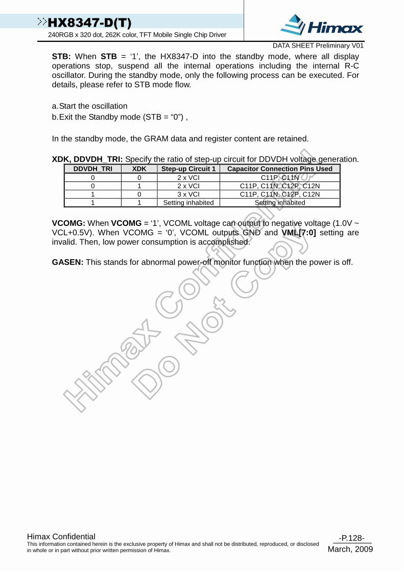
-P.128- Himax Confidential
March, 2009
This information contained herein is the exclusive property of Himax and shall not be distributed, reproduced, or disclosed in whole or in part without prior written permission of Himax.
HX8347-D(T) 240RGB x 320 dot, 262K color, TFT Mobile Single Chip Driver DATA SHEET Preliminary V01
STB: When STB = ‘1’, the HX8347-D into the standby mode, where all display operations stop, suspend all the internal operations including the internal R-C oscillator. During the standby mode, only the following process can be executed. For details, please refer to STB mode flow.
a. Start the oscillation b. Exit the Standby mode (STB = “0”) ,
In the standby mode, the GRAM data and register content are retained. XDK, DDVDH_TRI: Specify the ratio of step-up circuit for DDVDH voltage generation.
DDVDH_TRI XDK Step-up Circuit 1 Capacitor Connection Pins Used 0 0 2 x VCI C11P, C11N 0 1 2 x VCI C11P, C11N, C12P, C12N 1 0 3 x VCI C11P, C11N, C12P, C12N 1 1 Setting inhabited Setting inhabited
VCOMG: When VCOMG = ‘1’, VCOML voltage can output to negative voltage (1.0V ~ VCL+0.5V). When VCOMG = ‘0’, VCOML outputs GND and VML[7:0] setting are invalid. Then, low power consumption is accomplished. GASEN: This stands for abnormal power-off monitor function when the power is off.

-P.129- Himax Confidential
March, 2009
This information contained herein is the exclusive property of Himax and shall not be distributed, reproduced, or disclosed in whole or in part without prior written permission of Himax.
HX8347-D(T) 240RGB x 320 dot, 262K color, TFT Mobile Single Chip Driver DATA SHEET Preliminary V01
8.24 Read data register (PAGE0 -22h)
Figure 8.34 Read data register (PAGE0 -22h)
WD[17:0] : Transforms the data into 18-bit bus before written to GRAM through the write data register (WDR). After a write operation is issued, the address is automatically updated according to the AM and I/D bits.
RD[17:0]: Read 18-bit data from GRAM through the read data register (RDR). When the data is read by microcomputer, the first-word read immediately after the GRAM address setting is latched from the GRAM to the internal read-data latch. The data on the data bus (D17–0) becomes invalid and the second-word read is normal.

-P.130- Himax Confidential
March, 2009
This information contained herein is the exclusive property of Himax and shall not be distributed, reproduced, or disclosed in whole or in part without prior written permission of Himax.
HX8347-D(T) 240RGB x 320 dot, 262K color, TFT Mobile Single Chip Driver DATA SHEET Preliminary V01
8.25 VCOM control 1~3 register (PAGE0 -23~25h)
RB7
WWWW
RRRR////WWWW
1111
DNCDNCDNCDNC
VMF7
VMF6
VMF5
VMF4
VMF3
VMF2
VMF1
VMF0
RB6 RB5 RB4 RB3 RB2 RB1 RB0
RRRR 1111VMF7
VMF6
VMF5
VMF4
VMF3
VMF2
VMF1
VMF0
Figure 8.35 Vcom control 1 register (PAGE0 -23h)
RB7
WWWW
RRRR////WWWW
1111
DNCDNCDNCDNC
VMH7
VMH6
VMH5
VMH4
VMH3
VMH2
VMH1
VMH0
RB6 RB5 RB4 RB3 RB2 RB1 RB0
RRRR 1111VMH7
VMH6
VMH5
VMH4
VMH3
VMH2
VMH1
VMH0
Figure 8.36 Vcom control 2 register (PAGE0 -24h)
RB7
WWWW
RRRR////WWWW
1111
DNCDNCDNCDNC
VML7
VML6
VML5
VML4
VML3
VML2
VML1
VML0
RB6 RB5 RB4 RB3 RB2 RB1 RB0
RRRR 1111VML7
VML6
VML5
VML4
VML3
VML2
VML1
VML0
Figure 8.37 Vcom control 3 register (PAGE0 -25h)
This command is used to set VCOM Voltage include VCOM Low and VCOM High Voltage

-P.131- Himax Confidential
March, 2009
This information contained herein is the exclusive property of Himax and shall not be distributed, reproduced, or disclosed in whole or in part without prior written permission of Himax.
HX8347-D(T) 240RGB x 320 dot, 262K color, TFT Mobile Single Chip Driver DATA SHEET Preliminary V01
VMH[7:0]: Set the VCOMH voltage (High level voltage of VCOM). VCOM High voltage = Decimal(VMH[7:0])x0.015+2.5.
VMH7 VMH6 VMH5 VMH4 VMH3 VMH2 VMH1 VMH0 VCOMH (DDVDH_TRI=0)
VCOMH (DDVDH_TRI=1)
0 0 0 0 0 0 0 0 2.500 2.500 0 0 0 0 0 0 0 1 2.515 2.515 0 0 0 0 0 0 1 0 2.530 2.530 0 0 0 0 0 0 1 1 2.545 2.545 0 0 0 0 0 1 0 0 2.560 2.560 0 0 0 0 0 1 0 1 2.575 2.575 : : : : : : : : : : : : : : : : : : : : 1 0 0 1 0 0 1 1 4.705 4.705 1 0 0 1 0 1 0 0 4.720 4.720 1 0 0 1 0 1 0 1 4.735 4.735 1 0 0 1 0 1 1 0 4.750 4.750 1 0 0 1 0 1 1 1 4.765 4.765 1 0 0 1 1 0 0 0 4.780 4.780 1 0 0 1 1 0 0 1 4.795 4.795 1 0 0 1 1 0 1 0 4.800 4.810 1 0 0 1 1 0 1 1 4.800 4.825 1 0 0 1 1 1 0 0 4.800 4.840 1 0 0 1 1 1 0 1 4.800 4.855 : : : : : : : : 4.800 : 1 1 0 0 1 0 0 0 4.800 5.800 : : : : : : : : 4.800 5.800 1 1 1 1 1 1 1 0 4.800 5.800 1 1 1 1 1 1 1 1 Setting inhibited
Note: Internal VREF can be modified by customer’s req uest. default VREF=4.8 if DDVDH_TRI=0, and VREF=5.8 if DDVDH_TRI=1 VCOMH= Decimal(VMH[7:0])x0.015+2.5 *(VREF/4.8) if DDVDH_TRI=0 VCOMH= Decimal(VMH[7:0])x0.015+2.5 *(VREF/5.8) if DDVDH_TRI=1
VML[7:0]: Set the VCOML voltage (Low level voltage of VCOM). VCOM Low voltage = Decimal(VML[7:0])x0.015-2.5.
VML7 VML6 VML5 VML4 VML3 VML2 VML1 VML0 VCOML 0 0 0 0 0 0 0 0 -2.500 0 0 0 0 0 0 0 1 -2.485 0 0 0 0 0 0 1 0 -2.470 0 0 0 0 0 1 0 1 -2.455 : : : : : : : : : 1 0 1 0 0 0 1 1 -0.055 1 0 1 0 0 1 0 0 -0.040 1 0 1 0 0 1 0 1 -0.025 1 0 1 0 0 1 1 0 -0.010 1 0 1 0 0 1 1 1 VSS : : : : : : : : 1 1 1 1 1 1 1 1 VSS
Note: Internal VREF can be modified by customer’s req uest. default VREF=4.8 if DDVDH_TRI=0 and VREF=5.8 if DDVDH_TRI=1 VCOML= Decimal( VML[7:0])x0.015-2.5 *(VREF/4.8) if DDVDH_TRI=0, VCOML= Decimal (VML[7:0])x0.015-2.5 *(VREF/5.8) if DDVDH_TRI
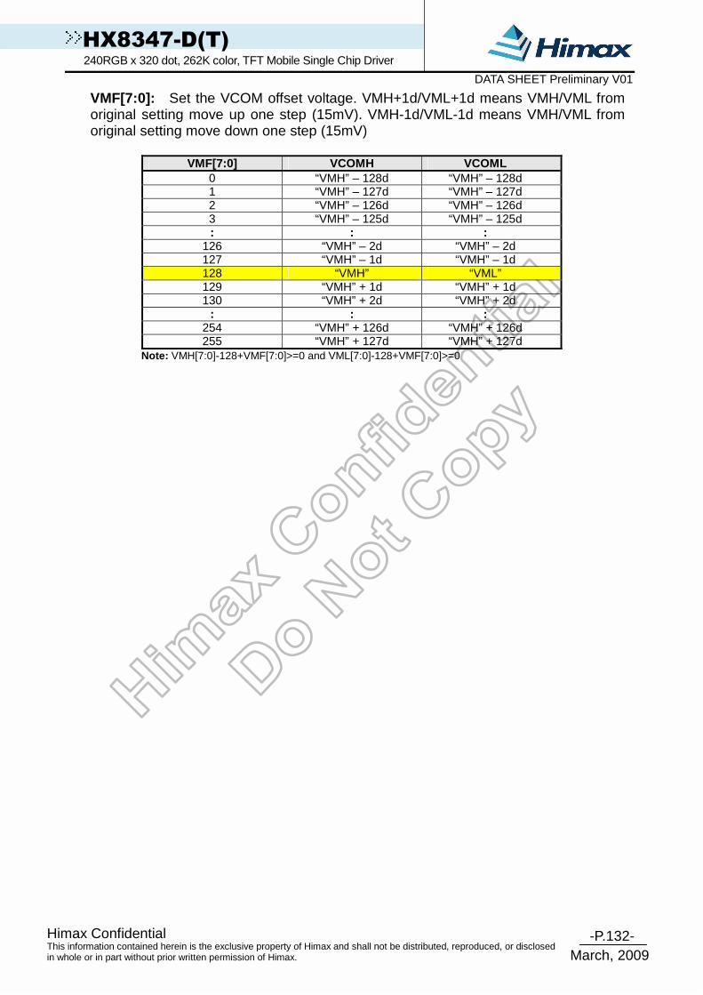
-P.132- Himax Confidential
March, 2009
This information contained herein is the exclusive property of Himax and shall not be distributed, reproduced, or disclosed in whole or in part without prior written permission of Himax.
HX8347-D(T) 240RGB x 320 dot, 262K color, TFT Mobile Single Chip Driver DATA SHEET Preliminary V01
VMF[7:0]: Set the VCOM offset voltage. VMH+1d/VML+1d means VMH/VML from original setting move up one step (15mV). VMH-1d/VML-1d means VMH/VML from original setting move down one step (15mV)
VMF[7:0] VCOMH VCOML 0 “VMH” – 128d “VMH” – 128d 1 “VMH” – 127d “VMH” – 127d 2 “VMH” – 126d “VMH” – 126d 3 “VMH” – 125d “VMH” – 125d : : :
126 “VMH” – 2d “VMH” – 2d 127 “VMH” – 1d “VMH” – 1d 128 “VMH” “VML” 129 “VMH” + 1d “VMH” + 1d 130 “VMH” + 2d “VMH” + 2d
: : : 254 “VMH” + 126d “VMH” + 126d 255 “VMH” + 127d “VMH” + 127d
Note: VMH[7:0]-128+VMF[7:0]>=0 and VML[7:0]-128+VMF[7:0]>=0

-P.133- Himax Confidential
March, 2009
This information contained herein is the exclusive property of Himax and shall not be distributed, reproduced, or disclosed in whole or in part without prior written permission of Himax.
HX8347-D(T) 240RGB x 320 dot, 262K color, TFT Mobile Single Chip Driver DATA SHEET Preliminary V01
8.26 Display control 1 register (PAGE0 -26h~R28h)
RB7
WWWW
RRRR////WWWW
1111
DNCDNCDNCDNC
* * * * ISC3 ISC2 ISC1 ISC0
RB6 RB5 RB4 RB3 RB2 RB1 RB0
RRRR 1111 * * * * ISC3 ISC2 ISC1 ISC0
Figure 8.38 Display control 1 register (PAGE0 -26h)
RB7
WWWW
RRRR////WWWW
1111
DNCDNCDNCDNC
PT1 PT0PTV1
PTV0
* * PTG REF
RB6 RB5 RB4 RB3 RB2 RB1 RB0
RRRR 1111 PT1 PT0PTV
1
PTV
0* * PTG REF
Figure 8.39 Display control 2 register (PAGE0 -27h)
RB7
WWWW
RRRR////WWWW
1111
DNCDNCDNCDNC
* * GON DTE D1 D0 * *
RB6 RB5 RB4 RB3 RB2 RB1 RB0
RRRR 1111 * * GON DTE D1 D0 0 0
Figure 8.40 Display control 3 register (PAGE0 -28h)
ISC[3:0]: Specify the scan cycle of gate driver when REF = ‘1’ in non-display area. Then scan cycle is set to an odd number from 0~31.The polarity is inverted every scan cycle.
ISC3 ISC2 ISC1 ISC0 Scan Cycle fFLM = 60Hz
0 0 0 0 1 frame 17ms
0 0 0 1 5 frames 83ms
0 0 1 0 9 frames 150ms
0 0 1 1 13 frames 217ms
0 1 0 0 17 frames 283ms
0 1 0 1 21 frames 350ms
0 1 1 0 25 frames 417ms
0 1 1 1 29 frames 483ms
1 0 0 0 33 frames 550ms
1 0 0 1 37 frames 616ms
1 0 1 0 41 frames 683ms
1 0 1 1 45 frames 750ms
1 1 0 0 49 frames 816ms
1 1 0 1 53 frames 883ms
1 1 1 0 57 frames 950ms
1 1 1 1 Setting inhibited
REF: Refresh display in non-display area in Partial mode enable bit. REF = ‘0’: Refresh display operation is disabling. REF = ‘1’: Refresh display operation is enabling.

-P.134- Himax Confidential
March, 2009
This information contained herein is the exclusive property of Himax and shall not be distributed, reproduced, or disclosed in whole or in part without prior written permission of Himax.
HX8347-D(T) 240RGB x 320 dot, 262K color, TFT Mobile Single Chip Driver DATA SHEET Preliminary V01
PTG: Specify the scan mode of gate driver in non-display area.
PTG Gate Outputs in Non-display Area
0 Normal Drive 1 Fixed VGL
PTV[1:0]: Specify the scan mode of VCOM in non-display area.
PTV1 PTV0 VCOM Outputs in Non-display Area
0 0 Normal Drive 0 1 Fixed to VCOML 1 0 Fixed to GND 1 1 Setting Inhibited
PT[1:0] : Specify the Non-display area source output in partial display mode.
Source Output Level Non-display Area Display area
PT1-0=(0,*) PT1-0=(1,0) PT1-0=(1,1) REV_panel GRAM Data VCOM =
“L” VCOM =
“H” VCOM =
“L” VCOM =
“H” VCOM =
“L” VCOM =
“H” VCOM = “L”
VCOM = “H”
1 (Normally
Black Panel)
18’h0000 :
18’h3FFF
V63P :
V0P
V0N :
V63N V63P V0N VSSD VSSD Hi-z Hi-z
0 (Normally
White Panel)
18’h0000 :
18’h3FFF
V0P :
V63P
V63N :
V0N V63P V0N VSSD VSSD Hi-z Hi-z
D[1:0]: When D1=‘1’, display is on; when D1=‘0’, display is off. When display is off, the display data is retained in the GRAM, and can be instantly displayed by setting D1 = ‘1’. When D1=‘0’, the display is off with the entire source outputs are set to the VSSD level. Because of this, the HX8347-D can control the charging current for the LCD with AC driving. Control the display on/off while control GON and DTE. When D[1:0]= ‘01’, the internal display of the HX8347-D is performed although the actual display is off. When D[1:0]= ‘00’, the internal display operation halts and the display is off.
D1 D0 Source Output HX8347-D Internal Display Operations Gate-Driver Control Signals
0 0 VSSD Halt Halt 0 1 VSSD Operate Operate 1 0 =PT(0,0) Operate Operate 1 1 Display Operate Operate

-P.135- Himax Confidential
March, 2009
This information contained herein is the exclusive property of Himax and shall not be distributed, reproduced, or disclosed in whole or in part without prior written permission of Himax.
HX8347-D(T) 240RGB x 320 dot, 262K color, TFT Mobile Single Chip Driver DATA SHEET Preliminary V01
GON, DTE:
GON DTE Gate Output 0 X VGH 1 0 VGL 1 1 VGH/VGL
PT1 PT0 REF ISC[3:0] Source Output VCOM Output Gate Output
0 x x -
Black Display ( REV_PANEL = ‘1’)
White Display (REV_PANEL = ‘0’)
Normal Driving Normal Driving
0 - GND PTV[1:0] PTG Non-refresh
cycle GND PTV[1:0] PTG
1 0 1
Refresh cycle
Black Display (REV_PANEL = ‘1’)
White Display (REV_PANEL = ‘0’)
Normal Driving Normal Driving
0 - Hi-z PTV[1:0] PTG Non-refresh
cycle Hi-z PTV[1:0] PTG
1 1 1
Refresh cycle
Black Display (REV_PANEL = ‘1’)
White Display (REV_PANEL = ‘0’)
Normal Driving Normal Driving

-P.136- Himax Confidential
March, 2009
This information contained herein is the exclusive property of Himax and shall not be distributed, reproduced, or disclosed in whole or in part without prior written permission of Himax.
HX8347-D(T) 240RGB x 320 dot, 262K color, TFT Mobile Single Chip Driver DATA SHEET Preliminary V01
8.27 Frame control register (PAGE0 -29h~R2Ch)
RB7
WWWW
RRRR////WWWW
1111
DNCDNCDNCDNC
I/P_RTN3
I/P_RTN2
I/P_RTN1
I/P_RTN0
N/P_RTN3
N/P_RTN2
N/P_RTN1
N/P_RTN0
RB6 RB5 RB4 RB3 RB2 RB1 RB0
RRRR 1111I/P_R
TN3
I/P_R
TN2
I/P_R
TN1
I/P_R
TN0
N/P_
RTN3
N/P_RTN_
2
N/P_
RTN1
N/P_
RTN0
Figure 8.41 Frame control 1 register (PAGE0 -29h) RB7
WWWW
RRRR////WWWW
1111
DNCDNCDNCDNC
* *I/P_
DIV1
I/P_
DIV0* *
N/P_
DIV1
N/P_
DIV0
RB6 RB5 RB4 RB3 RB2 RB1 RB0
RRRR 1111 * *I/P_
DIV1
I/P_
DIV0* *
N/P_
DIV1
N/P_
DIV0
Figure 8.42 Frame control 2 register (PAGE0 -2Ah)
RB7
WWWW
RRRR////WWWW
1111
DNCDNCDNCDNCN/P_DUM
7
N/P_DUM
6
N/P_DUM
5
N/P_DU
M4
N/P_DUM
3
N/P_DUM
2
N/P_DUM
1
N/P_DUM
0
RB6 RB5 RB4 RB3 RB2 RB1 RB0
RRRR 1111N/P_
DUM
7
N/P_
DUM
6
N/P_
DUM
5
N/P
_DU
M4
N/P_
DUM
3
N/P_
DUM
2
N/P_
DUM
1
N/P_
DUM
0 Figure 8.43 Frame control 3 register (PAGE0 -2Bh)
RB7
WWWW
RRRR////WWWW
1111
DNCDNCDNCDNCI/PI_DUM
7
I/PI_DUM
6
I/PI_DUM
5
I/PI_DU
M4
I/PI_DUM
3
I/PI_DUM
2
I/PI_DUM
1
I/PI_DUM
0
RB6 RB5 RB4 RB3 RB2 RB1 RB0
RRRR 1111I/PI_
DUM
7
I/PI_
DUM
6
I/PI_
DUM
5
I/PI
_DU
M4
I/PI_
DUM
3
I/PI_
DUM
2
I/PI_
DUM
1
I/PI_
DUM
0 Figure 8.44 Frame control 4 register (PAGE0 -2Ch)
N/P_DIV[1:0]: Specify the division ratio of internal clocks in Normal / Partial mode for internal operation. When used internal clock for the display operation, frame frequency can be adjusted with the N/P_RTN[3:0] bits (1H period clock cycle), N/P_DIV[1:0 ], and N/P_DUM[7:0] bits. I/PI_DIV[1:0]: Specify the division ratio of internal clocks in Idle (8-color) / Partial Idle mode for internal operation. When used internal clock for the display operation, frame frequency can be adjusted with the I/PI_RTN[3:0] bits(1H period clock cycle), I/PI_DIV[1:0 ], and I/PI_DUM[7:0] bits.
DIV1 DIV0 Division Ratio Internal Display Operation Clock Frequency
0 0 1 fosc / 1 0 1 2 fosc / 2 1 0 4 fosc / 4 1 1 8 fosc / 8
Note: fosc = R-C oscillation frequency
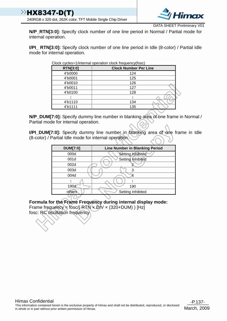
-P.137- Himax Confidential
March, 2009
This information contained herein is the exclusive property of Himax and shall not be distributed, reproduced, or disclosed in whole or in part without prior written permission of Himax.
HX8347-D(T) 240RGB x 320 dot, 262K color, TFT Mobile Single Chip Driver DATA SHEET Preliminary V01
N/P_RTN[3:0]: Specify clock number of one line period in Normal / Partial mode for internal operation. I/PI_ RTN[3:0]: Specify clock number of one line period in Idle (8-color) / Partial Idle mode for internal operation.
Clock cycles=1/internal operation clock frequency(fosc)
RTN[3:0] Clock Number Per Line 4’b0000 124 4’b0001 125 4’b0010 126 4’b0011 127 4’b0100 128
: : 4’b1110 134 4’b1111 135
N/P_DUM[7:0]: Specify dummy line number in blanking area of one frame in Normal / Partial mode for internal operation. I/PI_DUM[7:0]: Specify dummy line number in blanking area of one frame in Idle (8-color) / Partial Idle mode for internal operation.
DUM[7:0] Line Number in Blanking Period
000d Setting Inhibited 001d Setting Inhibited 002d 2 003d 3 004d 4
: : 190d 190 others Setting Inhibited
Formula for the Frame Frequency during internal dis play mode: Frame frequency = fosc/( RTN × DIV × (320+DUM) ) [Hz] fosc: RC oscillation frequency
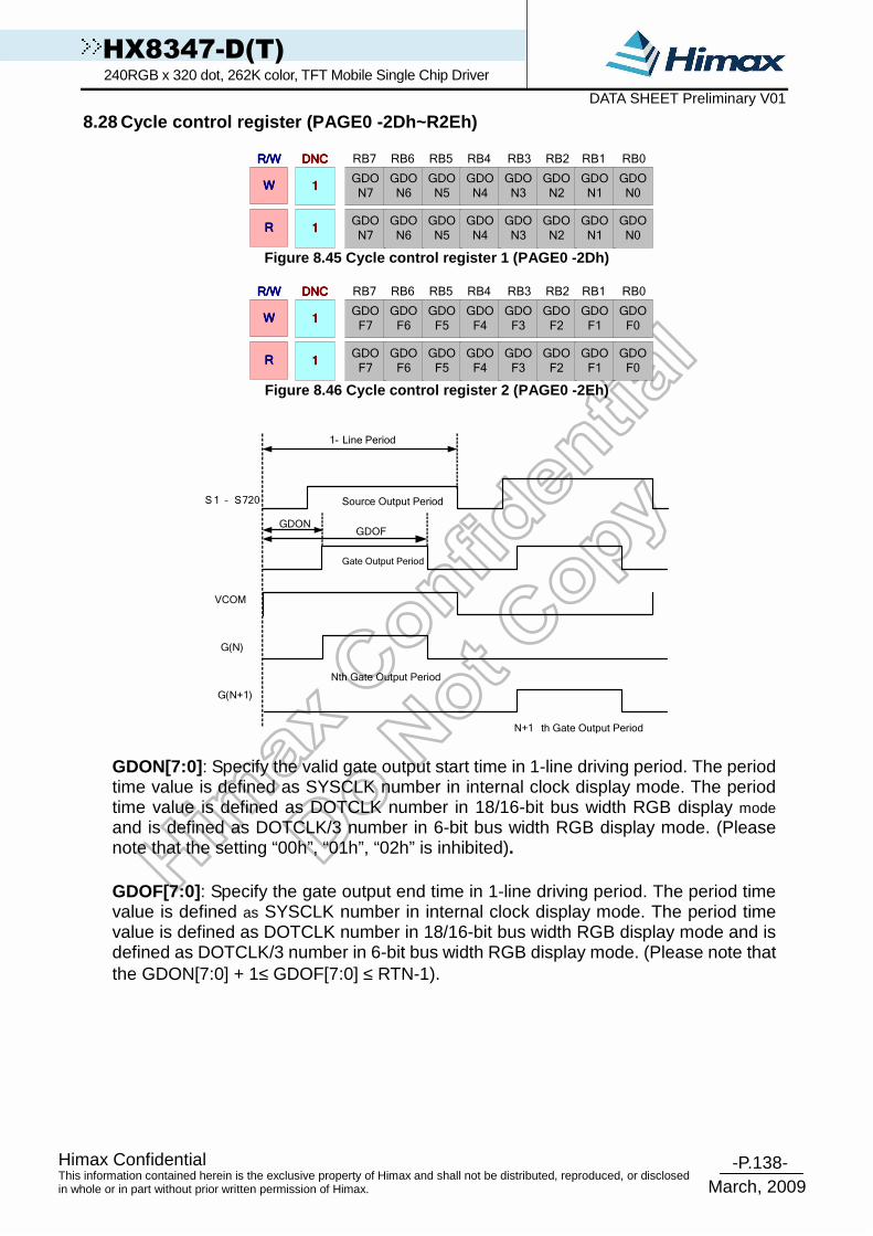
-P.138- Himax Confidential
March, 2009
This information contained herein is the exclusive property of Himax and shall not be distributed, reproduced, or disclosed in whole or in part without prior written permission of Himax.
HX8347-D(T) 240RGB x 320 dot, 262K color, TFT Mobile Single Chip Driver DATA SHEET Preliminary V01
8.28 Cycle control register (PAGE0 -2Dh~R2Eh)
RB7
WWWW
RRRR////WWWW
1111
DNCDNCDNCDNC
GDO
N7
GDO
N6
GDO
N5
GDO
N4
GDO
N3
GDO
N2
GDO
N1
GDO
N0
RB6 RB5 RB4 RB3 RB2 RB1 RB0
RRRR 1111GDO
N7
GDO
N6
GDO
N5
GDO
N4
GDO
N3
GDO
N2
GDO
N1
GDO
N0
Figure 8.45 Cycle control register 1 (PAGE0 -2Dh)
RB7
WWWW
RRRR////WWWW
1111
DNCDNCDNCDNC
GDO
F7
GDO
F6
GDO
F5
GDO
F4
GDO
F3
GDO
F2
GDO
F1
GDO
F0
RB6 RB5 RB4 RB3 RB2 RB1 RB0
RRRR 1111GDO
F7
GDO
F6
GDO
F5
GDO
F4
GDO
F3
GDO
F2
GDO
F1
GDO
F0
Figure 8.46 Cycle control register 2 (PAGE0 -2Eh)
1- Line Period
GDONGDOF
Source Output Period
Gate Output Period
Nth Gate Output Period
N+1 th Gate Output Period
S1 – S720
G(N)
G(N+1)
VCOM
GDON[7:0] : Specify the valid gate output start time in 1-line driving period. The period time value is defined as SYSCLK number in internal clock display mode. The period time value is defined as DOTCLK number in 18/16-bit bus width RGB display mode and is defined as DOTCLK/3 number in 6-bit bus width RGB display mode. (Please note that the setting “00h”, “01h”, “02h” is inhibited).
GDOF[7:0] : Specify the gate output end time in 1-line driving period. The period time value is defined as SYSCLK number in internal clock display mode. The period time value is defined as DOTCLK number in 18/16-bit bus width RGB display mode and is defined as DOTCLK/3 number in 6-bit bus width RGB display mode. (Please note that the GDON[7:0] + 1≤ GDOF[7:0] ≤ RTN-1).

-P.139- Himax Confidential
March, 2009
This information contained herein is the exclusive property of Himax and shall not be distributed, reproduced, or disclosed in whole or in part without prior written permission of Himax.
HX8347-D(T) 240RGB x 320 dot, 262K color, TFT Mobile Single Chip Driver DATA SHEET Preliminary V01
8.29 Display inversion register (PAGE0 -2Fh)
RB7
WWWW
RRRR////WWWW
1111
DNCDNCDNCDNC
*I/PI_
NW2
I/PI_
NW1
I/PI_
NW0*
N/P_
NW2
N/P_
NW1
N/P_
NW0
RB6 RB5 RB4 RB3 RB2 RB1 RB0
RRRR 1111 *I/PI_
NW2
I/PI_
NW1
I/PI_
NW0*
N/P_
NW2
N/P_
NW1
N/P_
NW0
Figure 8.47 Cycle control register (PAGE0 -2Fh)
N/P_ NW[2:0]: Specify LCD driving inversion type in Normal/ Partial mode. I/PI_ NW[2:0]: Specify LCD driving inversion type in Idle / Partial Idle mode.
NW[2:0] LCD Driving Inversion Type 0d Frame inversion 1d 1-line inversion 2d 2-line inversion 3d 3-line inversion : :
6d 6-line inversion 7d 7-line inversion

-P.140- Himax Confidential
March, 2009
This information contained herein is the exclusive property of Himax and shall not be distributed, reproduced, or disclosed in whole or in part without prior written permission of Himax.
HX8347-D(T) 240RGB x 320 dot, 262K color, TFT Mobile Single Chip Driver DATA SHEET Preliminary V01
8.30 RGB interface control register (PAGE0 -31h~R34 h)
RB7
WWWW
RRRR////WWWW
1111
DNCDNCDNCDNC
* * * * * *RCM
1
RCM
0
RB6 RB5 RB4 RB3 RB2 RB1 RB0
RRRR 1111 0 0 0 0 0 0RCM
1
RCM
0
Figure 8.48 RGB interface control register (PAGE0 - 31h)
RB7
WWWW
RRRR////WWWW
1111
DNCDNCDNCDNC
* * * * DPL HSPL VSPL EPL
RB6 RB5 RB4 RB3 RB2 RB1 RB0
RRRR 1111 0 0 0 * DPL HSPL VSPL EPL
Figure 8.49 RGB interface control register (PAGE0 - 32h)
RB7
WWWW
RRRR////WWWW
1111
DNCDNCDNCDNC
HBP7 HBP6 HBP5 HBP4 HBP3 HBP2 HBP1 HBP0
RB6 RB5 RB4 RB3 RB2 RB1 RB0
RRRR 1111 HBP7 HBP6 HBP5 HBP4 HBP3 HBP2 HBP1 HBP0
Figure 8.50 RGB interface control register (PAGE0 - 33h)
RB7
WWWW
RRRR////WWWW
1111
DNCDNCDNCDNC
HBP9 HBP8 VBP5 VBP4 VBP3 VBP2 VBP1 VBP0
RB6 RB5 RB4 RB3 RB2 RB1 RB0
RRRR 1111 HBP9 HBP8 VBP5 VBP4 VBP3 VBP2 VBP1 VBP0
Figure 8.51 RGB interface control register (PAGE0 - 34h)
This command is used to set RGB interface related register RCM[1:0]: RGB and MCU interface select.
RCM1 RCM0 Interface Select
0 x System Interface(1) 1 0 RGB Interface(1) (VS+HS+DE)
1 1 RGB Interface(2) (VS+HS) Note: (1) As RCM[1:0] bit be written, the external pin RCM[1:0] control is invalid.
EPL: Specify the polarity of ENABLE signal in RGB interface mode. EPL=’1’, the ENABLE signal is High active; EPL=0, the ENABLE signal is Low active. VSPL: The polarity of VSYNC pin. When VSPL=’0’, the VSYNC signal is Low active. When VSPL=1, the VSYNC signal is High active. HSPL: The polarity of HSYNC pin. When HSPL=’0’, the HSYNC signal is Low active. When HSPL=1, the HSYNC signal is High active. DPL: The polarity of DOTCLK pin. When DPL=’0’, the data is latched by the chip on the rising edge of DOTCLK signal. When DPL=’1’, the data is latched by the chip on the falling edge of DOTCLK signal.

-P.141- Himax Confidential
March, 2009
This information contained herein is the exclusive property of Himax and shall not be distributed, reproduced, or disclosed in whole or in part without prior written permission of Himax.
HX8347-D(T) 240RGB x 320 dot, 262K color, TFT Mobile Single Chip Driver DATA SHEET Preliminary V01
HBP and VBP are used to set vertical and horizontal back porch control in RGB I/F mode 2 (RCM[1:0]= ‘11’) (RGB I/F mode 1 is using DE signal as data enable signal) HBP[9:0] : Set the delay period from falling edge of HSYNC signal to first valid data in RGB I/F mode 2
HBP[9:0] No. of Clock Cycle of DOTCLK 00d Setting Inhibited 01d Setting Inhibited 02d 2 03d 3 04d 4
: : 1021d 1021 1022d 1022 1023d Setting Inhibited
VBP[5:0] : Set the delay period from falling edge of VSYNC signal to first valid line in RGB I/F mode 2
VBP[5:0] No. of Clock Cycle of HSYNC
00d Setting Inhibited 01d Setting Inhibited 02d 2 03d 3 04d 4
: : 125d 125 126d 126 127d Setting Inhibited
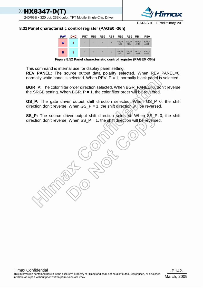
-P.142- Himax Confidential
March, 2009
This information contained herein is the exclusive property of Himax and shall not be distributed, reproduced, or disclosed in whole or in part without prior written permission of Himax.
HX8347-D(T) 240RGB x 320 dot, 262K color, TFT Mobile Single Chip Driver DATA SHEET Preliminary V01
8.31 Panel characteristic control register (PAGE0 - 36h)
RB7
WWWW
RRRR////WWWW
1111
DNCDNCDNCDNC
* * *SS_PA
NEL
GS_PA
NEL
REV_P
ANEL
BGR_P
ANEL*
RB6 RB5 RB4 RB3 RB2 RB1 RB0
RRRR 1111 * * *SS_PA
NEL
GS_PA
NEL
REV_P
ANEL
BGR_P
ANEL*
Figure 8.52 Panel characteristic control register ( PAGE0 -36h)
This command is internal use for display panel setting. REV_PANEL: The source output data polarity selected. When REV_PANEL=0, normally white panel is selected. When REV_P = 1, normally black panel is selected. BGR_P: The color filter order direction selected. When BGR_PANEL=0, don’t reverse the SRGB setting. When BGR_P = 1, the color filter order will be reversed. GS_P: The gate driver output shift direction selected. When GS_P=0, the shift direction don’t reverse. When GS_P = 1, the shift direction will be reversed. SS_P: The source driver output shift direction selected. When SS_P=0, the shift direction don’t reverse. When SS_P = 1, the shift direction will be reversed.

-P.143- Himax Confidential
March, 2009
This information contained herein is the exclusive property of Himax and shall not be distributed, reproduced, or disclosed in whole or in part without prior written permission of Himax.
HX8347-D(T) 240RGB x 320 dot, 262K color, TFT Mobile Single Chip Driver DATA SHEET Preliminary V01
8.32 OTP register (PAGE0 -38h ~ R3Ah)
Figure 8.53 OTP command 1 (PAGE0 -38h)
Figure 8.54 OTP command 2 (PAGE0 -39h)
Figure 8.55 OTP command 3 (PAGE0 -3Ah)
This command is used to set the OTP related setting. Please see OTP flow for detailed use. OTP_POR: for OTP read/write timing control OTP_OTPEN: 1’b1 to select 6.5V for OTP write operation. OTP_PPROG: 1’b1 to turn on OTP write mode. OTP_PWE: 1’b1 to write OTP. OTP_XA[4:0]; OTP_YA[2:0]: Select OTP writes address OTP_TM[1:0]: OTP Test mode register, In-house use. OTP_VRADJ[1:0]: OTP VPP2 adjusts register, In-house use.

-P.144- Himax Confidential
March, 2009
This information contained herein is the exclusive property of Himax and shall not be distributed, reproduced, or disclosed in whole or in part without prior written permission of Himax.
HX8347-D(T) 240RGB x 320 dot, 262K color, TFT Mobile Single Chip Driver DATA SHEET Preliminary V01
8.33 CABC control 1~4 register (PAGE0 -3Ch~3Fh)
RB7
W
R/W
1
DNC
DBV7
DBV6
DBV5
DBV4
DBV3
DBV2
DBV1
DBV0
RB6 RB5 RB4 RB3 RB2 RB1 RB0
R 1DBV
7DBV
6DBV
5DBV
4DBV
3DBV
2DBV
1DBV
0
Figure 8.56 CABC control 1 register (PAGE0 -3Ch)
RB7
W
R/W
1
DNC
BCTRL
DD BL
RB6 RB5 RB4 RB3 RB2 RB1 RB0
R 1 0 0BCTRL
0 DD BL 0 0
** * **
Figure 8.57 CABC control 2 register (PAGE0 -3Dh)
RB7
W
R/W
1
DNC
C1 C0
RB6 RB5 RB4 RB3 RB2 RB1 RB0
R 1 0 0 0 0 0 0 C1 C0
** ** **
Figure 8.58 CABC control 3 register (PAGE0 -3Eh)
RB7
W
R/W
1
DNC
CMB7
CMB6
CMB5
CMB4
CMB3
CMB2
CMB1
CMB0
RB6 RB5 RB4 RB3 RB2 RB1 RB0
R 1CMB
7CMB
6CMB
5CMB
4CMB
3CMB
2CMB
1CMB
0
Figure 8.59 CABC control 4 register (PAGE0 -3Fh)
These commands are used to set CABC parameter DBV[7:0]: The backlight PWM pulse output duty is equal to DBV[7:0]/255 x CABC_duty. BCTRL: Backlight Control Block On/Off, This bit is always used to switch brightness for display. ‘0’ = Off (Equal to DBV[7:0] = ‘00h’) ‘1’ = On (Brightness registers are active.) DD: Display Dimming (Only for manual brightness setting) ‘0’ : Display Dimming is off. ‘1’ : Display Dimming is on. BL: Backlight Control On/Off ‘0’ = Off (Completely turn off backlight circuit. Control lines must be low. ) ‘1’ = On

-P.145- Himax Confidential
March, 2009
This information contained herein is the exclusive property of Himax and shall not be distributed, reproduced, or disclosed in whole or in part without prior written permission of Himax.
HX8347-D(T) 240RGB x 320 dot, 262K color, TFT Mobile Single Chip Driver DATA SHEET Preliminary V01
Dimming function is adapted to the brightness registers for display when bit BCTRL is changed at DD=1, e.g. BCTRL: 0 -> 1 or 1-> 0. When BL bit change from “On” to “Off”, backlight is turned off without gradual dimming, even if dimming-on (DD=1) are selected.
C[1:0]: This command is used to set parameters for image content based adaptive brightness control functionality. There is possible to use 4 different modes for content adaptive image functionality, which are defined on a table below.
C1 C0 Function Note 0 0 Off - 0 1 User Interface Image - 1 0 Still Picture - 1 1 Moving Image -
CMB[7:0]: This command is used to set the minimum brightness value of the display for CABC function. In principle relationship is that 00h value means the lowest brightness for CABC and FFh value means the highest brightness for CABC.
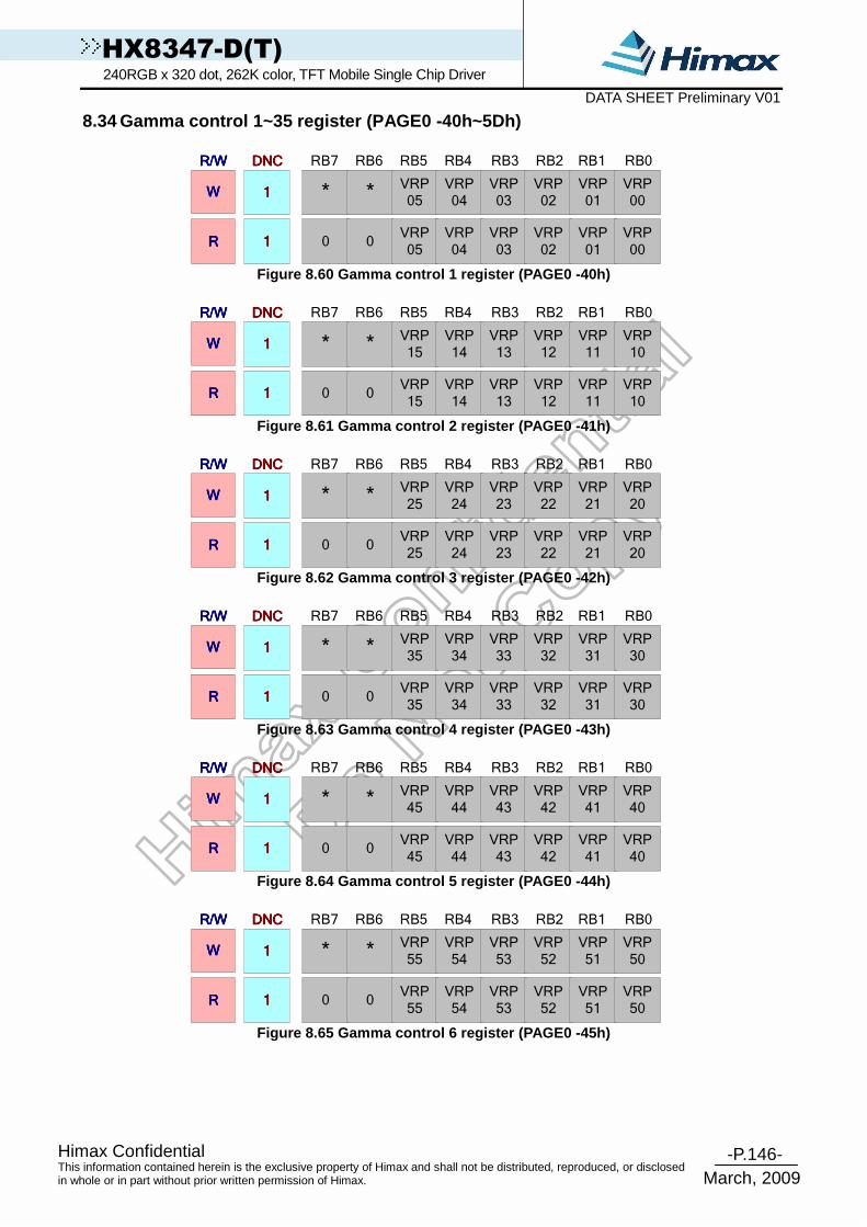
-P.146- Himax Confidential
March, 2009
This information contained herein is the exclusive property of Himax and shall not be distributed, reproduced, or disclosed in whole or in part without prior written permission of Himax.
HX8347-D(T) 240RGB x 320 dot, 262K color, TFT Mobile Single Chip Driver DATA SHEET Preliminary V01
8.34 Gamma control 1~35 register (PAGE0 -40h~5Dh)
RB7
WWWW
RRRR////WWWW
1111
DNCDNCDNCDNC
* *VRP05
VRP04
VRP03
VRP02
VRP01
VRP00
RB6 RB5 RB4 RB3 RB2 RB1 RB0
RRRR 1111 0 0VRP05
VRP04
VRP03
VRP02
VRP01
VRP00
Figure 8.60 Gamma control 1 register (PAGE0 -40h)
RB7
WWWW
RRRR////WWWW
1111
DNCDNCDNCDNC
* *VRP15
VRP14
VRP13
VRP12
VRP11
VRP10
RB6 RB5 RB4 RB3 RB2 RB1 RB0
RRRR 1111 0 0VRP15
VRP14
VRP13
VRP12
VRP11
VRP10
Figure 8.61 Gamma control 2 register (PAGE0 -41h)
RB7
WWWW
RRRR////WWWW
1111
DNCDNCDNCDNC
* *VRP25
VRP24
VRP23
VRP22
VRP21
VRP20
RB6 RB5 RB4 RB3 RB2 RB1 RB0
RRRR 1111 0 0VRP25
VRP24
VRP23
VRP22
VRP21
VRP20
Figure 8.62 Gamma control 3 register (PAGE0 -42h)
RB7
WWWW
RRRR////WWWW
1111
DNCDNCDNCDNC
* *VRP35
VRP34
VRP33
VRP32
VRP31
VRP30
RB6 RB5 RB4 RB3 RB2 RB1 RB0
RRRR 1111 0 0VRP35
VRP34
VRP33
VRP32
VRP31
VRP30
Figure 8.63 Gamma control 4 register (PAGE0 -43h)
RB7
WWWW
RRRR////WWWW
1111
DNCDNCDNCDNC
* *VRP45
VRP44
VRP43
VRP42
VRP41
VRP40
RB6 RB5 RB4 RB3 RB2 RB1 RB0
RRRR 1111 0 0VRP45
VRP44
VRP43
VRP42
VRP41
VRP40
Figure 8.64 Gamma control 5 register (PAGE0 -44h)
RB7
WWWW
RRRR////WWWW
1111
DNCDNCDNCDNC
* *VRP55
VRP54
VRP53
VRP52
VRP51
VRP50
RB6 RB5 RB4 RB3 RB2 RB1 RB0
RRRR 1111 0 0VRP55
VRP54
VRP53
VRP52
VRP51
VRP50
Figure 8.65 Gamma control 6 register (PAGE0 -45h)

-P.147- Himax Confidential
March, 2009
This information contained herein is the exclusive property of Himax and shall not be distributed, reproduced, or disclosed in whole or in part without prior written permission of Himax.
HX8347-D(T) 240RGB x 320 dot, 262K color, TFT Mobile Single Chip Driver DATA SHEET Preliminary V01
RB7
WWWW
RRRR////WWWW
1111
DNCDNCDNCDNC
*PRP05
PRP04
PRP03
PRP02
PRP01
PRP00
RB6 RB5 RB4 RB3 RB2 RB1 RB0
RRRR 1111 0PRP06
PRP05
PRP04
PRP03
PRP02
PRP01
PRP00
PRP06
Figure 8.66 Gamma control 7 register (PAGE0 -46h)
RB7
WWWW
RRRR////WWWW
1111
DNCDNCDNCDNC
*PRP15
PRP14
PRP13
PRP12
PRP11
PRP10
RB6 RB5 RB4 RB3 RB2 RB1 RB0
RRRR 1111 0PRP16
PRP15
PRP14
PRP13
PRP12
PRP11
PRP10
PRP16
Figure 8.67 Gamma control 8 register (PAGE0 -47h)
RB7
WWWW
RRRR////WWWW
1111
DNCDNCDNCDNC
* *PKP04
PKP03
PKP02
PKP01
PKP00
RB6 RB5 RB4 RB3 RB2 RB1 RB0
RRRR 1111 0 0 0PKP04
PKP03
PKP02
PKP01
PKP00
*
Figure 8.68 Gamma control 9 register (PAGE0 -48h)
RB7
WWWW
RRRR////WWWW
1111
DNCDNCDNCDNC
* *PKP14
PKP13
PKP12
PKP11
PKP10
RB6 RB5 RB4 RB3 RB2 RB1 RB0
RRRR 1111 0 0 0PKP14
PKP13
PKP12
PKP11
PKP10
*
Figure 8.69 Gamma control 10 register (PAGE0 -49h)
RB7
WWWW
RRRR////WWWW
1111
DNCDNCDNCDNC
* *PKP24
PKP23
PKP22
PKP21
PKP20
RB6 RB5 RB4 RB3 RB2 RB1 RB0
RRRR 1111 0 0 0PKP24
PKP23
PKP22
PKP21
PKP20
*
Figure 8.70 Gamma control 11 register (PAGE0 -4Ah)
RB7
WWWW
RRRR////WWWW
1111
DNCDNCDNCDNC
* *PKP34
PKP33
PKP32
PKP31
PKP30
RB6 RB5 RB4 RB3 RB2 RB1 RB0
RRRR 1111 0 0 0PKP34
PKP33
PKP32
PKP31
PKP30
*
Figure 8.71 Gamma control 12 register (PAGE0 -4Bh)

-P.148- Himax Confidential
March, 2009
This information contained herein is the exclusive property of Himax and shall not be distributed, reproduced, or disclosed in whole or in part without prior written permission of Himax.
HX8347-D(T) 240RGB x 320 dot, 262K color, TFT Mobile Single Chip Driver DATA SHEET Preliminary V01
RB7
WWWW
RRRR////WWWW
1111
DNCDNCDNCDNC
* *PKP44
PKP43
PKP42
PKP41
PKP40
RB6 RB5 RB4 RB3 RB2 RB1 RB0
RRRR 1111 0 0 0PKP44
PKP43
PKP42
PKP41
PKP40
*
Figure 8.72 Gamma control 13 register (PAGE0 -4Ch)
RB7
WWWW
RRRR////WWWW
1111
DNCDNCDNCDNC
* *VRN05
VRN04
VRN03
VRN02
VRN01
VRN00
RB6 RB5 RB4 RB3 RB2 RB1 RB0
RRRR 1111 0 0VRN05
VRN04
VRN03
VRN02
VRN01
VRN00
Figure 8.73 Gamma control 14 register (PAGE0 -50h)
RB7
WWWW
RRRR////WWWW
1111
DNCDNCDNCDNC
* *VRN15
VRN14
VRN13
VRN12
VRN11
VRN10
RB6 RB5 RB4 RB3 RB2 RB1 RB0
RRRR 1111 0 0VRN15
VRN14
VRN13
VRN12
VRN11
VRN10
Figure 8.74 Gamma control 15 register (PAGE0 -51h)
RB7
WWWW
RRRR////WWWW
1111
DNCDNCDNCDNC
* *VRN25
VRN24
VRN23
VRN22
VRN21
VRN20
RB6 RB5 RB4 RB3 RB2 RB1 RB0
RRRR 1111 0 0VRN25
VRN24
VRN23
VRN22
VRN21
VRN20
Figure 8.75 Gamma control 16 register (PAGE0 -52h)
RB7
WWWW
RRRR////WWWW
1111
DNCDNCDNCDNC
* *VRN35
VRN34
VRN33
VRN32
VRN31
VRN30
RB6 RB5 RB4 RB3 RB2 RB1 RB0
RRRR 1111 0 0VRN35
VRN34
VRN33
VRN32
VRN31
VRN30
Figure 8.76 Gamma control 17 register (PAGE0 -53h)
RB7
WWWW
RRRR////WWWW
1111
DNCDNCDNCDNC
* *VRN45
VRN44
VRN43
VRN42
VRN41
VRN40
RB6 RB5 RB4 RB3 RB2 RB1 RB0
RRRR 1111 0 0VRN45
VRN44
VRN43
VRN42
VRN41
VRN40
Figure 8.77 Gamma control 18 register (PAGE0 -54h)

-P.149- Himax Confidential
March, 2009
This information contained herein is the exclusive property of Himax and shall not be distributed, reproduced, or disclosed in whole or in part without prior written permission of Himax.
HX8347-D(T) 240RGB x 320 dot, 262K color, TFT Mobile Single Chip Driver DATA SHEET Preliminary V01
RB7
WWWW
RRRR////WWWW
1111
DNCDNCDNCDNC
* *VRN55
VRN54
VRN53
VRN52
VRN51
VRN50
RB6 RB5 RB4 RB3 RB2 RB1 RB0
RRRR 1111 0 0VRN55
VRN54
VRN53
VRN52
VRN51
VRN50
Figure 8.78 Gamma control 19 register (PAGE0 -55h)
RB7
WWWW
RRRR////WWWW
1111
DNCDNCDNCDNC
*PRN05
PRN04
PRN03
PRN02
PRN01
PRN00
RB6 RB5 RB4 RB3 RB2 RB1 RB0
RRRR 1111 0PRN06
PRN05
PRN04
PRN03
PRN02
PRN01
PRN00
PRN06
Figure 8.79 Gamma control 20 register (PAGE0 -56h)
RB7
WWWW
RRRR////WWWW
1111
DNCDNCDNCDNC
*PRN15
PRN14
PRN13
PRN12
PRN11
PRN10
RB6 RB5 RB4 RB3 RB2 RB1 RB0
RRRR 1111 0PRN16
PRN15
PRN14
PRN13
PRN12
PRN11
PRN10
PRN16
Figure 8.80 Gamma control 21 register (PAGE0 -57h)
RB7
WWWW
RRRR////WWWW
1111
DNCDNCDNCDNC
* *PKN04
PKN03
PKN02
PKN01
PKN00
RB6 RB5 RB4 RB3 RB2 RB1 RB0
RRRR 1111 0 0 0PKN04
PKN03
PKN02
PKN01
PKN00
*
Figure 8.81 Gamma control 22 register (PAGE0 -58h)
RB7
WWWW
RRRR////WWWW
1111
DNCDNCDNCDNC
* *PKN14
PKN13
PKN12
PKN11
PKN10
RB6 RB5 RB4 RB3 RB2 RB1 RB0
RRRR 1111 0 0 0PKN14
PKN13
PKN12
PKN11
PKN10
*
Figure 8.82 Gamma control 23 register (PAGE0 -59h)
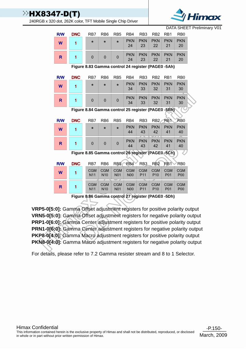
-P.150- Himax Confidential
March, 2009
This information contained herein is the exclusive property of Himax and shall not be distributed, reproduced, or disclosed in whole or in part without prior written permission of Himax.
HX8347-D(T) 240RGB x 320 dot, 262K color, TFT Mobile Single Chip Driver DATA SHEET Preliminary V01
RB7
WWWW
RRRR////WWWW
1111
DNCDNCDNCDNC
* *PKN24
PKN23
PKN22
PKN21
PKN20
RB6 RB5 RB4 RB3 RB2 RB1 RB0
RRRR 1111 0 0 0PKN24
PKN23
PKN22
PKN21
PKN20
*
Figure 8.83 Gamma control 24 register (PAGE0 -5Ah)
RB7
WWWW
RRRR////WWWW
1111
DNCDNCDNCDNC
* *PKN34
PKN33
PKN32
PKN31
PKN30
RB6 RB5 RB4 RB3 RB2 RB1 RB0
RRRR 1111 0 0 0PKN34
PKN33
PKN32
PKN31
PKN30
*
Figure 8.84 Gamma control 25 register (PAGE0 -5Bh)
RB7
WWWW
RRRR////WWWW
1111
DNCDNCDNCDNC
* *PKN44
PKN43
PKN42
PKN41
PKN40
RB6 RB5 RB4 RB3 RB2 RB1 RB0
RRRR 1111 0 0 0PKN44
PKN43
PKN42
PKN41
PKN40
*
Figure 8.85 Gamma control 26 register (PAGE0 -5Ch)
RB7
WWWW
RRRR////WWWW
1111
DNCDNCDNCDNC
CGMN11
CGMN01
CGMN00
CGMP11
CGMP10
CGMP01
CGMP00
RB6 RB5 RB4 RB3 RB2 RB1 RB0
RRRR 1111
CGMN10
CGMN11
CGMN01
CGMN00
CGMP11
CGMP10
CGMP01
CGMP00
CGMN10
Figure 8.86 Gamma control 27 register (PAGE0 -5Dh)
VRP5-0[5:0]: Gamma Offset adjustment registers for positive polarity output VRN5-0[5:0]: Gamma Offset adjustment registers for negative polarity output PRP1-0[6:0]: Gamma Center adjustment registers for positive polarity output PRN1-0[6:0]: Gamma Center adjustment registers for negative polarity output PKP8-0[4:0]: Gamma Macro adjustment registers for positive polarity output PKN8-0[4:0]: Gamma Macro adjustment registers for negative polarity output For details, please refer to 7.2 Gamma resister stream and 8 to 1 Selector.

-P.151- Himax Confidential
March, 2009
This information contained herein is the exclusive property of Himax and shall not be distributed, reproduced, or disclosed in whole or in part without prior written permission of Himax.
HX8347-D(T) 240RGB x 320 dot, 262K color, TFT Mobile Single Chip Driver DATA SHEET Preliminary V01
8.35 Mode control register (PAGE0 -60h)
RB7
WWWW
RRRR////WWWW
1111
DNCDNCDNCDNC
* * *TEMODE
TEON * * *
RB6 RB5 RB4 RB3 RB2 RB1 RB0
RRRR 1111 0 0 0TEMODE
TEON 0 0 0
Figure 8.87 Mode control register (PAGE0 -60h)
TEMODE: Specify the Tearing-Effect mode. When TEMODE = ‘0’: The Tearing Effect Output line (TE) consists of V-Blanking information only.
When TEMODE =’1’: The Tearing Effect Output Line (TE) consists of both V-Blanking and H-Blanking information
Note: During Stand by Mode with Tearing Effect Line On, Tearing Effect Output pin active low TEON: This command is used to turn ON the Tearing Effect output signal from the TE signal line.
8.36 ID Register (PAGE0 -R61h~R63h)
RB7
WWWW
RRRR////WWWW
1111
DNCDNCDNCDNC
ID17 ID16 ID15 ID14 ID13 ID12 ID11 ID10
RB6 RB5 RB4 RB3 RB2 RB1 RB0
RRRR 1111 ID17 ID16 ID15 ID14 ID13 ID12 ID11 ID10
Figure 8.88 ID1 Register (PAGE0 -61h)
RB7
WWWW
RRRR////WWWW
1111
DNCDNCDNCDNC
* ID26 ID25 ID24 ID23 ID22 ID21 ID20
RB6 RB5 RB4 RB3 RB2 RB1 RB0
RRRR 1111 1 ID26 ID25 ID24 ID23 ID22 ID21 ID20
Figure 8.89 ID2 Register (PAGE0 -62h)
RB7
WWWW
RRRR////WWWW
1111
DNCDNCDNCDNC
ID37 ID36 ID35 ID34 ID33 ID32 ID31 ID30
RB6 RB5 RB4 RB3 RB2 RB1 RB0
RRRR 1111 ID37 ID36 ID35 ID34 ID33 ID32 ID31 ID30
Figure 8.90 ID3 Register (PAGE0 -63h)
ID1~ID3: ID setting related register.
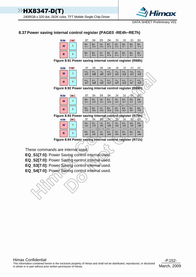
-P.152- Himax Confidential
March, 2009
This information contained herein is the exclusive property of Himax and shall not be distributed, reproduced, or disclosed in whole or in part without prior written permission of Himax.
HX8347-D(T) 240RGB x 320 dot, 262K color, TFT Mobile Single Chip Driver DATA SHEET Preliminary V01
8.37 Power saving internal control register (PAGE0 -RE4h~RE7h)
Figure 8.91 Power saving internal control register (R68h)
Figure 8.92 Power saving Internal control register (R69h)
Figure 8.93 Power saving Internal control register (R70h)
Figure 8.94 Power saving Internal control register (R71h)
These commands are internal used. EQ_S1[7:0]: Power Saving control internal used. EQ_S2[7:0]: Power Saving control internal used. EQ_S3[7:0]: Power Saving control internal used. EQ_S4[7:0]: Power Saving control internal used.

-P.153- Himax Confidential
March, 2009
This information contained herein is the exclusive property of Himax and shall not be distributed, reproduced, or disclosed in whole or in part without prior written permission of Himax.
HX8347-D(T) 240RGB x 320 dot, 262K color, TFT Mobile Single Chip Driver DATA SHEET Preliminary V01
8.38 Source OP control (PAGE0 -RE8h~E9h)
RB7
WWWW
RRRR////WWWW
1111
DNCDNCDNCDNC
OPON_N(7)
OPON_N(6)
OPON_N(5)
OPON_N(4)
OPON_N(3)
OPON_N(2)
OPON_N(1)
OPON_N(0)
RB6 RB5 RB4 RB3 RB2 RB1 RB0
RRRR 1111OPON_
N(7)
OPON_
N(6)
OPON_
N(5)
OPON_
N(4)
OPON_
N(3)
OPON_
N(2)
OPON_
N(1)
OPON_
N(0)
Figure 8.95 Source OP control register (PAGE0 -RE8h )
RB7
WWWW
RRRR////WWWW
1111
DNCDNCDNCDNC
OPON_N(7)
OPON_N(6)
OPON_N(5)
OPON_N(4)
OPON_N(3)
OPON_N(2)
OPON_N(1)
OPON_N(0)
RB6 RB5 RB4 RB3 RB2 RB1 RB0
RRRR 1111OPON_
N(7)
OPON_
N(6)
OPON_
N(5)
OPON_
N(4)
OPON_
N(3)
OPON_
N(2)
OPON_
N(1)
OPON_
N(0)
Figure 8.96 Source OP control register (PAGE0 -RE9h )
This command is used to set the Source OP output period. It will increase the driving ability of the source driver. For example, if the user has crosstalk issue, user can adjust this command for more driving ability, the ability is more when the setting is bigger. OPON_N[7:0] : Specify the Normal mode valid source OP output period in 1-line driving period. OPON_I[7:0] : Specify the IDLE mode valid source OP output period in 1-line driving period.

-P.154- Himax Confidential
March, 2009
This information contained herein is the exclusive property of Himax and shall not be distributed, reproduced, or disclosed in whole or in part without prior written permission of Himax.
HX8347-D(T) 240RGB x 320 dot, 262K color, TFT Mobile Single Chip Driver DATA SHEET Preliminary V01
8.39 Power control internal used (PAGE0 -REAh~ECh)
Figure 8.97 Power control internal used (1) registe r (PAGE0 -REAh)
Figure 8.98 Power control internal used (2) registe r (PAGE0 -REBh)
Figure 8.99 Source control internal used (1) regist er (PAGE0 -RECh)
Figure 8.100 Source control internal used (2) regis ter (PAGE0 -REDh)
These commands are internal used. PTBA[15:0]: Power control internal used. STBA[15:0]: Source Power control internal used.
8.40 Command page select register (RFFh)
RB7
WWWW
RRRR////WWWW
1111
DNCDNCDNCDNC
* * * * *
PAGE
_SEL1
PAGE
_SEL0
RB6 RB5 RB4 RB3 RB2 RB1 RB0
RRRR 1111
*
0 0 0 0 0PAGE_SEL1
PAGE_SEL0
0
Figure 8.101 Command page select register (RFFh)
PAGE_SEL[1:0]: Command set page select.
PAGE_SEL1 PAGE_SEL0 Command Page
0 0 Page 0 0 1 Page 1

-P.155- Himax Confidential
March, 2009
This information contained herein is the exclusive property of Himax and shall not be distributed, reproduced, or disclosed in whole or in part without prior written permission of Himax.
HX8347-D(T) 240RGB x 320 dot, 262K color, TFT Mobile Single Chip Driver DATA SHEET Preliminary V01
8.41 CABC control 5~7 register (PAGE1 – RC3h, RC5h, RC7h)
RB7
WWWW
RRRR////WWWW
1111
DNCDNCDNCDNC
0PWMDIV1
PWMDIV0
1 1INPLUS
1
RB6 RB5 RB4 RB3 RB2 RB1 RB0
RRRR 1111
PWMDIV2
0PWM
DIV1
PWM
DIV01 1
INPL
US1
PWM
DIV2
Figure 8.102 CABC control 5 (PAGE1 – RC3h)
RB7
WWWW
RRRR////WWWW
1111
DNCDNCDNCDNC
PWM_PERIO
D7
PWM_PERIO
D5
PWM_PERIO
D4
PWM_PERIO
D3
PWM_PERIO
D2
PWM_PERIO
D1
PWM_PERIO
D0
RB6 RB5 RB4 RB3 RB2 RB1 RB0
RRRR 1111
PWM_PERIO
D6
PWM_
PERIO
D7
PWM_
PERIO
D5
PWM_
PERIO
D4
PWM_
PERIO
D3
PWM_
PERIO
D2
PWM_
PERIO
D1
PWM_
PERIO
D0
PWM_
PERIO
D6
Figure 8.103 CABC control 6 (PAGE1 – RC5h)
RB7
WWWW
RRRR////WWWW
1111
DNCDNCDNCDNC
0DIM_F
RAME5
DIM_F
RAME4
DIM_F
RAME3
DIM_F
RAME2
DIM_F
RAME1
DIM_F
RAME0
RB6 RB5 RB4 RB3 RB2 RB1 RB0
RRRR 1111
DIM_FRAME
6
0DIM_FRAME5
DIM_FRAME4
DIM_FRAME3
DIM_FRAME2
DIM_FRAME1
DIM_FRAME0
DIM_F
RAME
6
Figure 8.104 CABC control 7 (PAGE1 – RC7h)
PWM_DIV[2:0]: Internal PWM_CLK divider for CABC clock.
PWM_DIV[2:0] Divider 0 PWM_CLK/1 1 PWM_CLK/2 2 PWM_CLK/4 3 PWM_CLK/8 4 PWM_CLK/16 5 PWM_CLK/32 6 PWM_CLK/64 7 PWM_CLK/128
Note: PWM_CLK is OSC frequency in system interface and DOTCLK in RGB interface.
INVPULS: The backlight PWM output polarity select. ‘0’, The backlight PWM output is low level active. ‘1’, The backlight PWM output is high level active.
PWM_PERIOD[7:0] : The backlight PWM output period setting. Backlight PWM output period = 1 / (PWM_CLK / clock divider (PWMDIV)) x
(255x(PWM_PERIOD[7:0]+1)) DIM_FRAME[6:0] : Manual brightness setting dimming period.

-P.156- Himax Confidential
March, 2009
This information contained herein is the exclusive property of Himax and shall not be distributed, reproduced, or disclosed in whole or in part without prior written permission of Himax.
HX8347-D(T) 240RGB x 320 dot, 262K color, TFT Mobile Single Chip Driver DATA SHEET Preliminary V01
8.42 Gain select register 0~8 (PAGE1 – RCBh~D3h)
RB7
WWWW
RRRR////WWWW
1111
DNCDNCDNCDNC
*DBG05
DBG04
DBG03
DBG02
DBG01
DBG00
RB6 RB5 RB4 RB3 RB2 RB1 RB0
RRRR 1111
DBG06
0DBG05
DBG04
DBG03
DBG02
DBG01
DBG00
DBG06
Figure 8.105 Gain select register 0 (PAGE1 – RCBh)
RB7
WWWW
RRRR////WWWW
1111
DNCDNCDNCDNC
*DBG15
DBG14
DBG13
DBG12
DBG11
DBG10
RB6 RB5 RB4 RB3 RB2 RB1 RB0
RRRR 1111
DBG16
0DBG15
DBG14
DBG13
DBG12
DBG11
DBG10
DBG16
Figure 8.106 Gain select register 1 (PAGE1 – RCCh)
RB7
WWWW
RRRR////WWWW
1111
DNCDNCDNCDNC
*DBG25
DBG24
DBG23
DBG22
DBG21
DBG20
RB6 RB5 RB4 RB3 RB2 RB1 RB0
RRRR 1111
DBG26
0DBG25
DBG24
DBG23
DBG22
DBG21
DBG20
DBG26
Figure 8.107 Gain select register 2 (PAGE1 – RCDh)
RB7
WWWW
RRRR////WWWW
1111
DNCDNCDNCDNC
*DBG35
DBG34
DBG33
DBG32
DBG31
DBG30
RB6 RB5 RB4 RB3 RB2 RB1 RB0
RRRR 1111
DBG36
0DBG35
DBG34
DBG33
DBG32
DBG31
DBG30
DBG36
Figure 8.108 Gain select register 3 (PAGE1 – RCEh)
RB7
WWWW
RRRR////WWWW
1111
DNCDNCDNCDNC
*DBG45
DBG44
DBG43
DBG42
DBG41
DBG40
RB6 RB5 RB4 RB3 RB2 RB1 RB0
RRRR 1111
DBG46
0DBG45
DBG44
DBG43
DBG42
DBG41
DBG40
DBG46
Figure 8.109 Gain select register 4 (PAGE1 – RCFh)
RB7
WWWW
RRRR////WWWW
1111
DNCDNCDNCDNC
*DBG55
DBG54
DBG53
DBG52
DBG51
DBG50
RB6 RB5 RB4 RB3 RB2 RB1 RB0
RRRR 1111
DBG56
0DBG55
DBG54
DBG53
DBG52
DBG51
DBG50
DBG56
Figure 8.110 Gain select register 5 (PAGE1 – RD0h)
RB7
WWWW
RRRR////WWWW
1111
DNCDNCDNCDNC
*DBG65
DBG64
DBG63
DBG62
DBG61
DBG60
RB6 RB5 RB4 RB3 RB2 RB1 RB0
RRRR 1111
DBG66
0DBG65
DBG64
DBG63
DBG62
DBG61
DBG60
DBG66
Figure 8.111 Gain select register 6 (PAGE1 – RD1h)

-P.157- Himax Confidential
March, 2009
This information contained herein is the exclusive property of Himax and shall not be distributed, reproduced, or disclosed in whole or in part without prior written permission of Himax.
HX8347-D(T) 240RGB x 320 dot, 262K color, TFT Mobile Single Chip Driver DATA SHEET Preliminary V01
RB7
WWWW
RRRR////WWWW
1111
DNCDNCDNCDNC
*DBG75
DBG74
DBG73
DBG72
DBG71
DBG70
RB6 RB5 RB4 RB3 RB2 RB1 RB0
RRRR 1111
DBG76
0DBG75
DBG74
DBG73
DBG72
DBG71
DBG70
DBG76
Figure 8.112 Gain select register 7 (PAGE1 – RD2h)
RB7
WWWW
RRRR////WWWW
1111
DNCDNCDNCDNC
*DBG85
DBG84
DBG83
DBG82
DBG81
DBG80
RB6 RB5 RB4 RB3 RB2 RB1 RB0
RRRR 1111
DBG86
0DBG85
DBG84
DBG83
DBG82
DBG81
DBG80
DBG86
Figure 8.113 Gain select register 8 (PAGE1 – RD3h)
DBG0~8[6:0] : Gain select register 0~8
UI ST MV
DBG0 24 40 40 DBG1 24 3C 3C DBG2 24 38 38 DBG3 23 34 34 DBG4 23 33 33 DBG5 23 32 32 DBG6 22 2B 2D DBG7 22 24 2B DBG8 22 22 28
DBGX Duty DBGX Duty DBGX Duty
20 100.00% 30 66.67% 40 49.80%
21 96.86% 31 65.10% 22 94.12% 32 63.92% 23 91.37% 33 62.75% 24 89.02% 34 61.57% 25 86.27% 35 60.39% 26 84.31% 36 59.22% 27 81.96% 37 58.04% 28 80.00% 38 56.86% 29 78.04% 39 56.08% 2A 76.08% 3A 54.90% 2B 74.51% 3B 54.12% 2C 72.55% 3C 53.33% 2D 70.98% 3D 52.16% 2E 69.41% 3E 51.37% 2F 67.84% 3F 50.59%

-P.158- Himax Confidential
March, 2009
This information contained herein is the exclusive property of Himax and shall not be distributed, reproduced, or disclosed in whole or in part without prior written permission of Himax.
HX8347-D(T) 240RGB x 320 dot, 262K color, TFT Mobile Single Chip Driver DATA SHEET Preliminary V01
9. Layout Recommendation
NR
ES
ET
NR
D_E
DN
C_S
CL
NW
R_R
NW
3. The input pin must be fixed IOVCC or GND when no use. Refer to "Pin Description". NC
S
VC
L
DD
VD
H
C3
1P
VG
L
VG
H
C3
1N
VR
EG
1
VC
OM
VC
OM
L
VC
OM
H
VD
DD
TE
IM0
IM1
IM2
OS
C
DNC1DNC
VCOM1VCOM
NCS1NCS
VDDD1VDDD
NWR_SCL1NWR_SCL
VG
H
VTEST1VTEST
DDVDH1DDVDH
IM3IM1
C08
C31NC31P
IM2IM2
VCOMH1VCOMH
U1
HX8347-D (BUMP UP)
VG
L
C1
1P
VP
P_
OT
P
HS
YN
CD
OT
CL
KD
EN
RE
SE
TN
RD
_EN
WR
_RN
WIM
3IM
2
C2
2N
DD
VD
H
C2
2P
G2
G4
G32
0
G1
G3
G31
7G
319
S1
S2
S3
S72
0S
719
S71
8
G6
G31
8
G31
5
G5
VG
H
C1
1N
CO
NN
CO
NN
VC
OM
NC
S
VS
SA
DN
C_S
CL
VS
SC
VC
I
VS
SD
VS
YN
C
DU
MM
Y27
DU
MM
Y
DU
MM
Y23
DU
MM
Y24
S26
2S
263
S36
1S
265
S26
6S
267
C2
1PC
21N
IM0
SD
AD
17
TE
ST
10D
16
D1
5T
ES
T9
D1
4D
13
TE
ST
8D
12
D1
1T
ES
T7
D1
0D
9T
ES
T6
D8
D7
TE
ST
5D
6D
5T
ES
T4
D4
D3
TE
ST
3D
2D
1D
0T
ES
T2
TE
CA
BC
_PW
M_O
UT
OS
CIO
VC
CV
DD
D
C1
2PC
12N
C3
1PC
31N
VC
L
VR
EG
1
VT
ES
T
VM
ON
I
VC
OM
H_D
UM
MY
VC
OM
L_D
UM
MY
RC
M1
RC
M0
SR
GB
SM
XS
MY
IFS
EL
VC
OM
_DU
MM
Y
IM1
TE
ST
1
CA
BC
PW
MO
UT
IM1IM3
C12P
C02 (OPEN)
C12N
TE1TE
VCOML1VCOML
VCL1VCL
NRESET1NRESET
VT
ES
T
VGL1VGL
NR
ES
ET
IOV
CC
NRD_E1NRD
VC
I
NR
ES
ET
NR
D
VREG1VREG1
NW
R_
SC
L
VGH1VGH
GN
D
OSC1OSC
240RGB x 320 TFT Panel
IM4IM0
IM3
C2
1N
C01
C2
1P
C11P C11N
VT
ES
T
C10
1- -1
IM3 IM2 IM1
8080 MCU 16-bits Parallel type II
0
0
IM0
DB
8
DB
10D
B9
DB
7
0
Interface mode
DB
12D
B11
VD
DD
00
DB
13D
B14
100
DB
15
IOV
CC
3-WIRE SERIAL INTERFACE
8080 MCU 8-bits Parallel type II
DB
17
DB
16
SD
A
TE
00
0
1 0
110
C2
2NC
22P
DB
1D
B0
DB
4D
B3
DB
2
01-
DB
6D
B5
ID
01 0 0
001
01
1
01
101 1 8080 MCU 9-bits Parallel type II
C09
8080 MCU 16-bits Parallel type I
8080 MCU 18-bits Parallel type II
8080 MCU 9-bits Parallel type I
VSSA
VSSD
IM0
IM1
IM2
IM3
GN
D
IM2
IM0
VC
I
IM1
4-WIRE SERIAL INTERFACE
8080 MCU 8-bits Parallel type I
C06
VP
P_
OT
P
C01 ( C11P/N )
C02 ( C12P/N )(Optional)
Recommended spec.Capacitor
C04 ( C21P/N )
C03 ( DDVDH )
1uF / 6.3Volt.
C06 ( VGH )
C05 ( C22P/N )
C09 ( VCL)
C08 ( C31P/N )
C07 ( VGL )
1uF / 10 Volt.
1uF / 6.3Volt.
C10 ( VDDD )
1uF / 10 Volt.
1uF / 10 Volt.
1uF / 6.3 Volt.
1uF / 16 Volt.
1uF / 25 Volt.
1uF / 6.3 Volt.
1uF / 6.3 Volt.
2. SDI pin is I/O pin. SDO is no use.
CONN1CONN1
CO
NN
1
VC
OM
LV
CO
MH
SD
A
CA
BC
PW
M
DB
11
CONN2CONN2
CO
NN
2
VS
SD
VS
SA
VS
SC
DB
13
DB
15 N
CS
DB
5
DB
9D
B8
DB
10
DB
14
DB
12
DB
7
DB
4
NW
R_S
CL
DB
3
DB
6
DB
0
DB
2D
B1
DN
C_S
CL
NR
D
DB
16 G
ND
TE
DB
17
VR
EG
1C07
VG
L VC
L
DD
VD
H
CO
NN
1C
ON
N2
CA
BC
PW
M
VSSC
C03
C04
C21NC21P
SRGB="0" S1,S2,S3="B,G,R"
C31
P
C12
PC
12N
C31
N
SMX="0" S720->S1
RCM[1:0]="0x" MPU I/F
SMY="0" G1->G320
CA
BC
PW
M
PWMPWM
VP
P_O
TP
VPP_OTP1VPP_OTP
IFSEL="0" REGISTER-CONTENT INTERFACE
DN
C_S
CL
C05
8080 MCU 18-bits Paralle type I
C22P
NC
S
GND1GND
GND2GND
J1
FPC60-0.5-4.0L
VC
I1
VC
I2
GN
D3
VC
C4
IOV
CC
5
nRE
SE
T6
DB
1713
DB
1614
DB
1515
DB
1416
DB
1317
DB
1218
DB
1119
DB
1020
DB
921
DB
822
DB
723
DB
624
DB
525
DB
426
DB
327
DB
228
DB
129
DB
030
nRD
_E
31
NW
R_R
NW
32
DN
C33
nCS
34
FLM
35
GN
D36
PW
M_O
UT
37
VS
YN
C38
HS
YN
C39
DO
TC
LK
40
EN
AB
LE
41
SD
O42
SD
I43
NC
44
NC
45
NC
46
NC
47
NC
48
NC
49
NC
50
NC
51
EX
TC
52
DB
S53
IM3
54
IM2
55
IM1
56
IM0
57
GN
D58
BL+
/NC
59
BL_
GN
D/N
C60
DB
237
DB
228
DB
219
DB
2010
DB
1911
DB
1812
IM3
1. VCI, IOVCC are separated from different power so urce to get better display quality.
IOV
CC
VC
I
VCI1VCI
IOVCC1IOVCC
C22N
Figure 9.1 Layout recommendation of HX8347-D MPU mo de
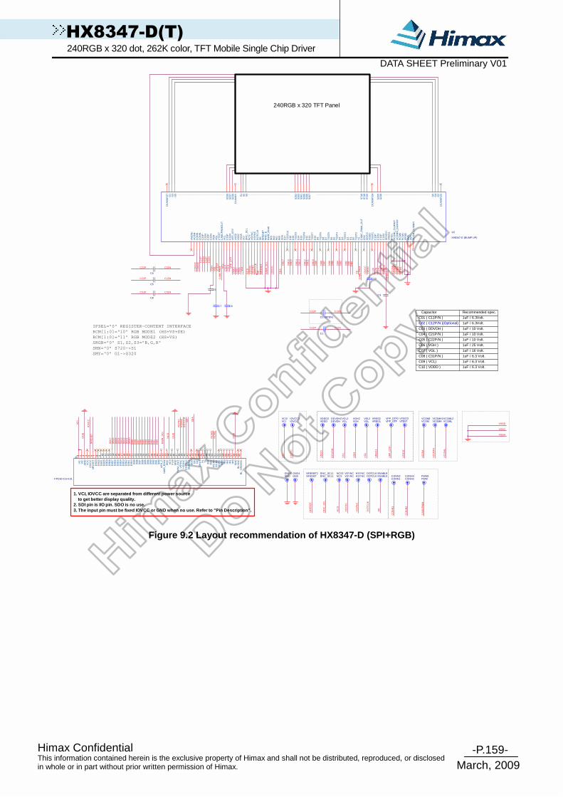
-P.159- Himax Confidential
March, 2009
This information contained herein is the exclusive property of Himax and shall not be distributed, reproduced, or disclosed in whole or in part without prior written permission of Himax.
HX8347-D(T) 240RGB x 320 dot, 262K color, TFT Mobile Single Chip Driver DATA SHEET Preliminary V01
Capacitor
C01 ( C11P/N )
C02 ( C12P/N )(Optional)
Recommended spec.
C04 ( C21P/N )
C03 ( DDVDH )
1uF / 6.3Volt.
C07 ( VGL )
C06 ( VGH )
C05 ( C22P/N )
C09 ( VCL)
C08 ( C31P/N )
1uF / 10 Volt.
1uF / 6.3Volt.
C10 ( VDDD )
1uF / 25 Volt.
1uF / 10 Volt.
1uF / 10 Volt.
1uF / 6.3 Volt.
1uF / 16 Volt.
1uF / 6.3 Volt.
1uF / 6.3 Volt.
RC
M0
VC
OM
LV
CO
MH
RC
M1
CA
BC
PW
M
CA
BC
PW
M
VR
EG
1
SRGB="0" S1,S2,S3="B,G,R"
SMY="0" G1->G320SMX="0" S720->S1
C3
DD
VD
H
VT
ES
T
C11
NC
11P
C12
PC
12N
VS
YN
C
DE
DO
TC
LK
HS
YN
C
HSYNCHSYNC
ENABLEENABLE
DOTCLKDOTCLK
VSYNCVSYNC
RC
M0
RC
M1
DO
TC
LK
C21
PC
21N
CO
NN
2 C22
NC
22P
CO
NN
2
NR
ES
ET
DN
C_S
CL
2. SDI pin is I/O pin. SDO is no use.3. The input pin must be fixed IOVCC or GND when no use. Refer to "Pin Description".
DD
VD
H
VC
L
NC
S
VR
EG
1
VG
H
VG
L
VC
OM
VC
OM
L
VD
DD
VC
OM
H
C31
PC
31N
C8
C31NC31P
VCOM2VCOM
NCS2NCS
VDDD2VDDD
DNC_SCL1DNC_SCL1
DDVDH2DDVDH
VCOMH2VCOMH
C12NC12P
C2 (OPEN)
VG
H
NR
ES
ET
240RGB x 320 TFT Panel
C11P
C1
C11N
C10
VCOML2VCOML
DB
8
VCL2VCL
DB
9
DB
7
NRESET2NRESET
DB
10
VGL2VGL
VD
DD
DB
12D
B11
DB
13D
B14
IOV
CC
DB
17
DB
16D
B15
IOV
CC
SD
A
TE
NR
ES
ET
VC
I
VREG2VREG1
VGH2VGH
GN
D
DB
1D
B0
DB
3
DB
2
DB
6D
B5
DB
4
C9
IOV
CC
VC
I
HS
YN
CV
SY
NC
C6
DE
VP
P_O
TP
VS
SD
VS
SA
VS
SC
C7
VC
L
VG
LC21NC21P
C4
C5
NC
S
C22P C22N
GN
D
SD
A VTEST2VTEST
NC
S VSSA
GN
D
VSSD
VSSC
GND3GND
GND4GND
J2
FPC60-0.5-4.0L
VC
I1
VC
I2
GN
D3
VC
C4
IOV
CC
5
nRE
SE
T6
DB
171
3
DB
161
4
DB
151
5
DB
141
6
DB
131
7
DB
121
8
DB
111
9
DB
102
0
DB
92
1
DB
82
2
DB
72
3
DB
62
4
DB
52
5
DB
42
6
DB
32
7
DB
22
8
DB
12
9
DB
03
0
nRD
_E3
1
NW
R_R
NW
32
DN
C3
3
nCS
34
FLM
35
GN
D3
6
PW
M_O
UT
37
VS
YN
C3
8
HS
YN
C3
9
DO
TC
LK4
0
EN
AB
LE4
1
SD
O4
2
SD
I4
3
NC
44
SH
UT
45
RL
46
TB
47
IDM
48
RE
V4
9
RC
M0
50
RC
M1
51
EX
TC
52
DB
S5
3
IM3
54
IM2
55
IM1
56
IM0
57
GN
D5
8
BL+
/NC
59
BL_
GN
D/N
C6
0
DB
237
DB
228
DB
219
DB
201
0
DB
191
1
DB
181
2
1. VCI, IOVCC are separated from different power so urce to get better display quality.
VC
I
IOV
CC
VCI2VCI
IOVCC2IOVCC
VT
ES
T
DB
11
DB
5
DB
15
DB
13
DB
10
DB
8D
B9
DB
12
DB
14
DB
3D
B4
DB
7
DB
2
DB
0
DB
6
DB
16
DB
1
NW
R_S
CL
DB
17
VS
YN
C
RCM[1:0]="11" RGB MODE2 (HS+VS)RCM[1:0]="10" RGB MODE1 (HS+VS+DE)
HS
YN
C
NW
R_
SC
L
DO
TC
LK
IFSEL="0" REGISTER-CONTENT INTERFACE
U2
HX8347-D (BUMP UP)
VG
L
C11
P
VP
P_
OT
P
HS
YN
CD
OT
CLK
DE
NR
ES
ET
NR
D_E
NW
R_R
NW
IM3
IM2
DD
VD
H
G2
G4
G32
0
G1
G3
G31
7G
319
S1
S2
S3
S72
0S
719
S71
8
G6
G31
8
G31
5
G5
VG
H
C11
N
CO
NN
CO
NN
VC
OM
NC
S
VS
SA
DN
C_S
CL
VS
SC
VC
I
VS
SD
VS
YN
C
DU
MM
Y27
DU
MM
Y
DU
MM
Y23
DU
MM
Y24
S26
2S
263
S36
1S
265
S26
6S
267
C21
PC
21N
IM0
SD
AD
17T
ES
T10
D16
D15
TE
ST
9D
14D
13T
ES
T8
D12
D11
TE
ST
7D
10D
9T
ES
T6
D8
D7
TE
ST
5D
6D
5T
ES
T4
D4
D3
TE
ST
3D
2D
1D
0T
ES
T2
TE
CA
BC
_PW
M_O
UT
OS
CIO
VC
CV
DD
D
C12
PC
12N
C31
PC
31N
VC
L
VR
EG
1
VT
ES
T
VM
ON
I
VC
OM
H_
DU
MM
YV
CO
ML_
DU
MM
Y
RC
M1
RC
M0
SR
GB
SM
XS
MY
IFS
EL
VC
OM
_DU
MM
Y
IM1
TE
ST
1
CA
BC
PW
MO
UT
C22
PC
22N
DE
CO
NN
1
CONN3CONN1
CO
NN
2
CONN4CONN2
CA
BC
PW
M
PWM1PWM
VPP_OTP2VPP_OTP
VP
P_O
TP
Figure 9.2 Layout recommendation of HX8347-D (SPI+R GB)
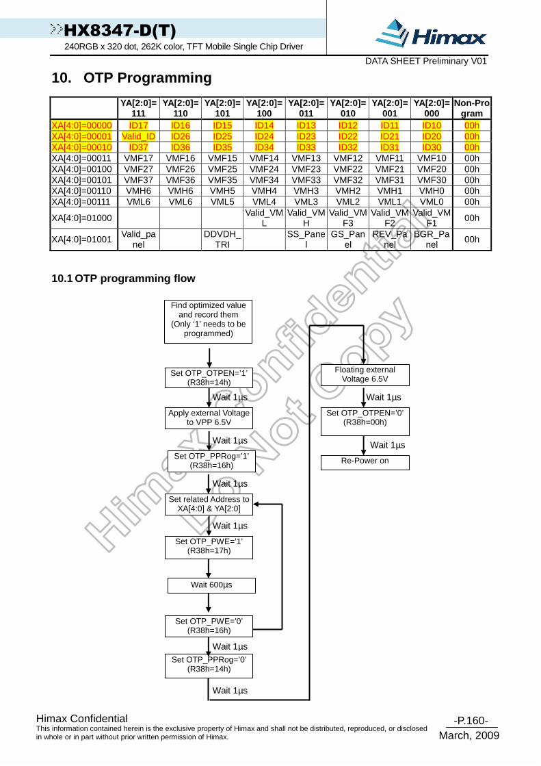
-P.160- Himax Confidential
March, 2009
This information contained herein is the exclusive property of Himax and shall not be distributed, reproduced, or disclosed in whole or in part without prior written permission of Himax.
HX8347-D(T) 240RGB x 320 dot, 262K color, TFT Mobile Single Chip Driver DATA SHEET Preliminary V01
10. OTP Programming
YA[2:0]=111
YA[2:0]=110
YA[2:0]=101
YA[2:0]=100
YA[2:0]=011
YA[2:0]=010
YA[2:0]=001
YA[2:0]=000
Non-Program
XA[4:0]=00000 ID17 ID16 ID15 ID14 ID13 ID12 ID11 ID10 00h XA[4:0]=00001 Valid_ID ID26 ID25 ID24 ID23 ID22 ID21 ID20 00h XA[4:0]=00010 ID37 ID36 ID35 ID34 ID33 ID32 ID31 ID30 00h XA[4:0]=00011 VMF17 VMF16 VMF15 VMF14 VMF13 VMF12 VMF11 VMF10 00h XA[4:0]=00100 VMF27 VMF26 VMF25 VMF24 VMF23 VMF22 VMF21 VMF20 00h XA[4:0]=00101 VMF37 VMF36 VMF35 VMF34 VMF33 VMF32 VMF31 VMF30 00h XA[4:0]=00110 VMH6 VMH6 VMH5 VMH4 VMH3 VMH2 VMH1 VMH0 00h XA[4:0]=00111 VML6 VML6 VML5 VML4 VML3 VML2 VML1 VML0 00h
XA[4:0]=01000 Valid_VM
L Valid_VM
H Valid_VM
F3 Valid_VM
F2 Valid_VM
F1 00h
XA[4:0]=01001 Valid_pa
nel DDVDH_
TRI SS_Pane
l GS_Pan
el REV_Pa
nel BGR_Pa
nel 00h
10.1 OTP programming flow
Find optimized value and record them
(Only ‘1’ needs to be programmed)
Set OTP_OTPEN=’1’ (R38h=14h)
Set OTP_PPRog=’1’ (R38h=16h)
Apply external Voltage to VPP 6.5V
Set related Address to XA[4:0] & YA[2:0]
Set OTP_PWE=’1’ (R38h=17h)
Set OTP_PWE=’0’ (R38h=16h)
Floating external Voltage 6.5V
Set OTP_PPRog=’0’ (R38h=14h)
Set OTP_OTPEN=’0’ (R38h=00h)
Re-Power on
Wait 600µs
Wait 1µs
Wait 1µs
Wait 1µs
Wait 1µs
Wait 1µs
Wait 1µs
Wait 1µs
Wait 1µs
-P.161- Himax Confidential
March, 2009
This information contained herein is the exclusive property of Himax and shall not be distributed, reproduced, or disclosed in whole or in part without prior written permission of Himax.
HX8347-D(T) 240RGB x 320 dot, 262K color, TFT Mobile Single Chip Driver DATA SHEET Preliminary V01
Note: Valid bit must program if user want use this OTP function

-P.162- Himax Confidential
March, 2009
This information contained herein is the exclusive property of Himax and shall not be distributed, reproduced, or disclosed in whole or in part without prior written permission of Himax.
HX8347-D(T) 240RGB x 320 dot, 262K color, TFT Mobile Single Chip Driver DATA SHEET Preliminary V01
OTP programming example (VMF=15h)
15h=8’b00010101 only YA=000,010 and
100need program
Set OTP_OTPEN=’1’ (R38h=14h)
Set OTP_PPRog=’1’ (R38h=16h)
Apply external Voltage to VPP 6.5V
Set related Address to XA & YA
(R39h=00h,R3Ah=08h)
Set OTP_PWE=’1’ (R38h=17h)
Set OTP_PWE=’0’ (R38h=16h)
Floating external Voltage 6.5V
Set OTP_PPRog=’0’ (R38h=14h)
Set OTP_OTPEN=’0’ (R38h=00h)
Re-Power on
Wait 600µs
Wait 1µs
Wait 1µs
Wait 1µs
Wait 1µs
Wait 1µs
Wait 1µs
Wait 1µs
Wait 1µs
Set related Address to XA & YA
(R39h=00h,R3Ah=03h)
Set OTP_PWE=’1’ (R38h=17h)
Set OTP_PWE=’0’ (R38h=16h)
Wait 600µs
Wait 1µs
Set related Address to XA & YA
(R39h=02h,R3Ah=03h)
Set OTP_PWE=’1’ (R38h=17h)
Set OTP_PWE=’0’ (R38h=16h)
Wait 600µs
Wait 1us
Wait 1µs
Wait 1us
Set related Address to XA & YA
(R39h=04h,R3Ah=03h)
Set OTP_PWE=’1’ (R38h=17h)
Set OTP_PWE=’0’ (R38h=16h)
Wait 600µs
Wait 1µs
Wait 1µs

-P.163- Himax Confidential
March, 2009
This information contained herein is the exclusive property of Himax and shall not be distributed, reproduced, or disclosed in whole or in part without prior written permission of Himax.
HX8347-D(T) 240RGB x 320 dot, 262K color, TFT Mobile Single Chip Driver DATA SHEET Preliminary V01
11. Electrical Characteristic
11.1 Absolute maximum ratings
Item Symbol Unit Value Note Power Supply Voltage 1 IOVCC~VSSD V -0.3 to +4.6 Note(1),(2) Power Supply Voltage 2 VCI ~ VSSA V -0.3 to +4.6 Note(3) Power Supply Voltage 3 DDVDH ~ VSSA V -0.3 to +6.6 Note(4) Power Supply Voltage 4 VSSA ~ VCL V -0.3 to +4.6 Note(5) Power Supply Voltage 5 DDVDH ~ VCL V -0.3 to +9 Note(6) Power Supply Voltage 6 VGH ~ VSSA V -0.3 to +18.5 Note(7) Power Supply Voltage 7 VSSA ~ VGL V 0 to -16.5 Note(8) Logic Input Voltage VIN V -0.3 to IOVCC+0.5 - Logic Output Voltage Vo V -0.3 to IOVCC+0.5 - Operating Temperature Topr -40 to +85 Note(9),(10) Storage Temperature Tstg -55 to +110 Note(9),(10)
Note: (1) IOVCC, VSSD must be maintained. (2) To make sure IOVCC ≥ VSSD. (3) To make sure VCI ≥ VSSA. (4) To make sure DDVDH ≥ VSSA. (5) To make sure VSSA ≥ VCL. (6) To make sure DDVDH ≥ VCL. (7) To make sure VGH ≥ VSSA. (8) To make sure VSSA ≥ VGL
VGH +|VGL| < 32V (9) For die and wafer products, specified up to +85 . (10) This temperature specifications apply to the TCP package.
Table 11.1 Absolute maximum ratings
11.2 ESD protection level
Mode Test Condition Protection Level Unit Human Body Model C=100pF, R=1.5kΩ ±2.0K V Machine Model C=200pF, R=0.0Ω ±200 V
Table 11.2 ESD protection level

-P.164- Himax Confidential
March, 2009
This information contained herein is the exclusive property of Himax and shall not be distributed, reproduced, or disclosed in whole or in part without prior written permission of Himax.
HX8347-D(T) 240RGB x 320 dot, 262K color, TFT Mobile Single Chip Driver DATA SHEET Preliminary V01
11.3 Maximum layout resistance
Name Type Maximum Series Resistance Unit
IOVCC Power supply 10 Ω VCI Power supply 10 Ω VSSA,VSSC Power supply 10 Ω VSSD Power supply 10 Ω VPP_OTP Power supply 10 Ω OSC Input 100 Ω IM[3:0], SMX,SMY,SRGB,RCM0,RCM1,IFSEL Input 100 Ω NRD_E, NWR_RNW, DNC_SCL, NCS, SDA Input 100 Ω NRESET Input 100 Ω TE, CABC_PWM_OUT Output 100 Ω DB[17:0], I/O 100 Ω DOTCLK, DE, VSYNC, HSYNC Input 100 Ω
VGH Capacitor connection
10 Ω
VGL Capacitor connection
10 Ω
VCL Capacitor connection
10 Ω
DDVDH Capacitor connection 10 Ω
VDDD Capacitor connection
10 Ω
VREG1 Capacitor connection
30 Ω
C11P, C11N, C12P, C12N Capacitor connection
10 Ω
C31P, C12N Capacitor connection
10 Ω
C21P, C21N Capacitor connection 15 Ω
C22P, C22N Capacitor connection
15 Ω
TEST[10:1] Input 100 Ω VCOMH_DUMMY, VCOML_DUMMY,DUMMY Dummy 100 Ω VTEST,VMONI Test Pin 100 Ω

-P.165- Himax Confidential
March, 2009
This information contained herein is the exclusive property of Himax and shall not be distributed, reproduced, or disclosed in whole or in part without prior written permission of Himax.
HX8347-D(T) 240RGB x 320 dot, 262K color, TFT Mobile Single Chip Driver DATA SHEET Preliminary V01
11.4 DC characteristics
Spec. Parameter Symbol Conditions Min. Typ. Max.
Unit
Power & Operating Voltages IO Operating voltage IOVCC I/O supply voltage 1.65 1.8 3.3 Driver Operating voltage VCI Operation voltage 2.3 2.8 3.3
VREG1 Triple Pump 3.3 4.65 4.8 Source Drive Voltage VREG1 Dual Pump 3.3 4.65 5.8
IVGH=100µA (Typ:BT=001) VCI=2.8
Dual Pump 9.5 14.25 -
Gate Drive High Voltage VGH IVGH=100uA (Typ:BT=001)
VCI=2.8 Triple Pump
11.6 17.39 -
IVGL=100µA (Typ:BT=001) VCI=2.8
Dual Pump -6.85 -9.5 -
Gate Drive Low Voltage VGL IVGL=100µA (Typ:BT=001)
VCI=2.8 Triple Pump
-8.46 -11.59 -
Drive Supply Voltage |VGH-VGL| - - - 30
V
Input / Output High level input voltage VIH - 0.7IOVCC - IOVCC Low level input voltage VIL - VSSD - 0.3IOVCC High level output voltage VOH IOH=-1.0mA 0.8IOVCC - IOVCC Low level output voltage VOL IOL=+1.0mA VSSD - 0.2IOVCC
V
Input leakage current IIL - -1 - 1 µA
Oscillator frequency fOSC
Frame rate at 65hz,default Vs and Hs
setting TA=25
2.76 2.85 2.94 MHz
Booster(VCI=2.8V) Dual Pump
IDDVDH=1mA 4.8 5.0 5.2 DDVDH boost voltage1 DDVDH
Triple Pump IDDVDH=1mA
5.9 6.1 6.3
VCL boost voltage VCL ICL=-300µA -2.5 -2.65 2.75
V
VCOM Generator(VCI=2.8V) No load,
Dual Pump 2.5 4.4 7.3 V
VCOM amplitude VCOM No load
Triple Pump 2.5 4.4 8.3 V
No load Dual Pump 2.5 3.205 4.8 V
VCOM high level VCOMH No load
Triple Pump 2.5 3.205 5.8 V
VCOM low level VCOML No load -2.5 -1.195 VSSD V Source Driver(Typ:T A=25 VCI=2.8v)
VSSD+1.0 ~ VREG1-1.0 - +/-10 +/-20 mV
Output voltage deviation (mean value) DVOS
VSSD+0.1V ~ VSSD+1.0
VREG1-1.0 ~ VREG1-0.1V
- +/-30 +/-50 mV
Output voltage range VOS - 0.1 - DDVDH-0.1 V Output offset voltage Voff - +/-30 +/-50 mV
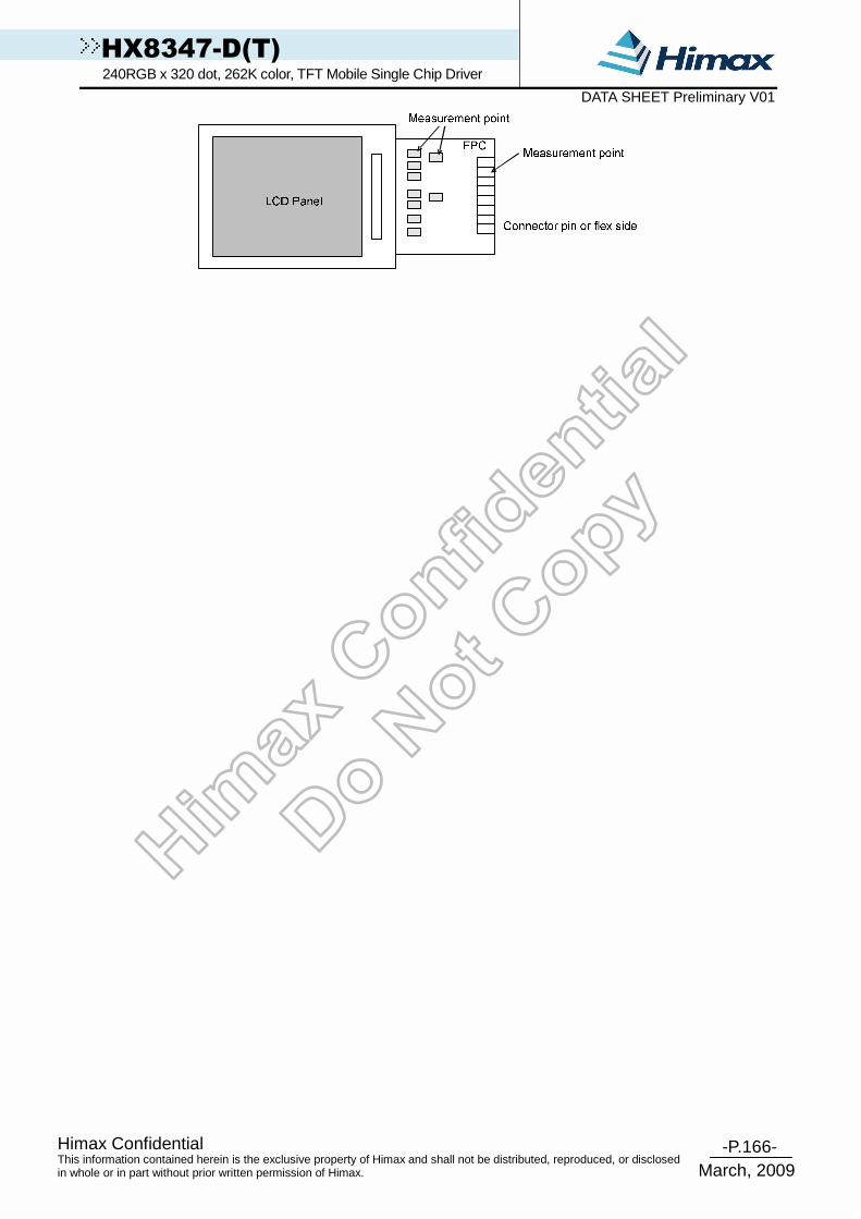
-P.166- Himax Confidential
March, 2009
This information contained herein is the exclusive property of Himax and shall not be distributed, reproduced, or disclosed in whole or in part without prior written permission of Himax.
HX8347-D(T) 240RGB x 320 dot, 262K color, TFT Mobile Single Chip Driver DATA SHEET Preliminary V01

-P.167- Himax Confidential
March, 2009
This information contained herein is the exclusive property of Himax and shall not be distributed, reproduced, or disclosed in whole or in part without prior written permission of Himax.
HX8347-D(T) 240RGB x 320 dot, 262K color, TFT Mobile Single Chip Driver DATA SHEET Preliminary V01
11.4.1 Current consumption
Current Consumption Typical Worst Case Host
I/F Mode of
operation Frame
Frequency Inversion
Mode Image
Memory Data Access Control
(MY:MX:MV) VCI
(mA) IOVCC(
mA) VCI
(mA) IOVCC(mA)
1-line Black X;X;X 3.48 0.21 3.85 0.33
1-line 1x1 checker board X;X;X 2.82 0.21 3.06 0.33
1-line 4x4 checker board X;X;X 2.76 0.33 3.12 0.42
1-line Gray_Scale
Top to Bottom
X;X;X 2.57 0.22 3.00 0.33
Normal Mode On 60Hz
1-line 20B80W X;X;X 3.05 0.21 3.50 0.32 Idle Mode On 60Hz 1-line 20B80W X;X;X 2.40 0.17 2.74 0.25 Partial Mode On (48 lines) 60Hz 1-line Grey
Levels X;X;X 0.86 0.11 1.35 0.18
1-line 8x8 checker board X;X;X 0.99 0.09 1.12 0.15 Partial Mode On
(48 lines) Idle Mode On
60Hz 1-line Worst
pattern X;X;X 1.01 0.09 1.20 0.15
Standby Mode N/A N/A N/A X;X;X 0.00059 0.00452 0.010 0.080
Hos
t int
erfa
ce N
OT
act
ive
Deep Standby Mode N/A N/A N/A X;X;X 0.0005 0.001 0.005 0.010
0;0;0 3.29 0.98 3.89 1.30 0;0;1 3.29 0.98 3.89 1.30 0;1;0 3.29 0.98 3.89 1.30 0;1;1 3.29 0.98 3.89 1.30 1;0;0 3.29 0.98 3.89 1.30 1;0;1 3.29 0.98 3.89 1.30 1;1;0 3.29 0.98 3.89 1.30
262k Colors Worst pattern CPU
Access @ 15fps
1;1;1 3.29 0.98 3.89 1.30 0;0;0 3.28 1.54 3.88 1.88 0;0;1 3.28 1.54 3.88 1.88 0;1;0 3.28 1.54 3.88 1.88 0;1;1 3.28 1.54 3.88 1.88 1;0;0 3.28 1.54 3.88 1.88 1;0;1 3.28 1.54 3.88 1.88 1;1;0 3.28 1.54 3.88 1.88
Hos
t int
erfa
ce a
ctiv
e
Normal Mode On 60Hz 1-line
262k Colors Worst pattern CPU
Access @ 25fps
1;1;1 3.28 1.54 3.88 1.88 Table 11.3 Current consumption
Typical Case: TA = 25oC IOVCC=1.8V VCI = 2.8V CMO 2.6” panel Worst Case: TA = -30 to70oC IOVCC = 1.65V to 1.95V VCI = 2.3V to 3.3V Includes Process Variance.

-P.168- Himax Confidential
March, 2009
This information contained herein is the exclusive property of Himax and shall not be distributed, reproduced, or disclosed in whole or in part without prior written permission of Himax.
HX8347-D(T) 240RGB x 320 dot, 262K color, TFT Mobile Single Chip Driver DATA SHEET Preliminary V01
11.5 AC Characteristics 11.5.1 Parallel interface characteristics (8080-ser ies MPU)
Figure 11.1 Parallel interface characteristics (808 0-series MPU)
(VSSA=0V, IOVCC=1.65V to 3.3V, VCI=2.3V to 3.3V,TA = -30 to 70°C)
Signal Symbol Parameter Min. Max. Unit Description
DNC_SCL tAST tAHT
Address setup time Address hold time (Write/Read)
0 10
- -
ns -
NCS
tCHW tCS tRCS tRCSFM tCSF tCSH
Chip select “H” pulse width Chip select setup time (Write) Chip select setup time (Read ID) Chip select setup time (Read FM) Chip select wait time (Write/Read) Chip select hold time
0 15 45 355 10 10
- - - - - -
ns -
NWR_SCL tWC tWRH tWRL
Write cycle Control pulse “H” duration Control pulse “L” duration
66 15 15
- - -
ns -
NRD(ID) tRC tRDH tRDL
Read cycle (ID) Control pulse “H” duration (ID) Control pulse “L” duration (ID)
160 90 45
- - -
ns When read ID data
NRD(FM) tRCFM tRDHFM tRDLFM
Read cycle (FM) Control pulse “H” duration (FM) Control pulse “L” duration (FM)
450 90 355
- - -
ns When read from frame memory
DB17 to DB0
tDST tDHT tRAT tRATFM tODH
Data setup time Data hold time Read access time (ID) Read access time (FM) Output disable time
10 10 - -
20
- -
40 340 80
ns
For maximum CL=30pF For minimum CL=8pF
Note: The input signal rise time and fall time (tr, tf) is specified at 15 ns or less. Logic high and low levels are specified as 30% and 70% of IOVCC for Input signals.

-P.169- Himax Confidential
March, 2009
This information contained herein is the exclusive property of Himax and shall not be distributed, reproduced, or disclosed in whole or in part without prior written permission of Himax.
HX8347-D(T) 240RGB x 320 dot, 262K color, TFT Mobile Single Chip Driver DATA SHEET Preliminary V01
Figure 11.2 Chip select timing
Figure 11.3 Write to read and read to write timing
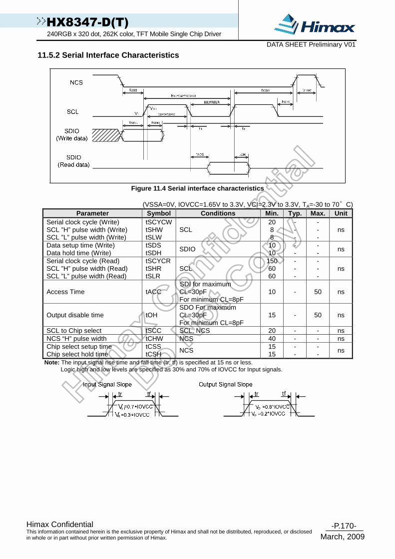
-P.170- Himax Confidential
March, 2009
This information contained herein is the exclusive property of Himax and shall not be distributed, reproduced, or disclosed in whole or in part without prior written permission of Himax.
HX8347-D(T) 240RGB x 320 dot, 262K color, TFT Mobile Single Chip Driver DATA SHEET Preliminary V01
11.5.2 Serial Interface Characteristics
Figure 11.4 Serial interface characteristics
(VSSA=0V, IOVCC=1.65V to 3.3V, VCI=2.3V to 3.3V, TA=-30 to 70°C)
Parameter Symbol Conditions Min. Typ. Max. Unit Serial clock cycle (Write) SCL ”H” pulse width (Write) SCL ”L” pulse width (Write)
tSCYCW tSHW tSLW
SCL 20 8 8
- - -
- - -
ns
Data setup time (Write) Data hold time (Write)
tSDS tSDH
SDIO 10 10
- -
- -
ns
Serial clock cycle (Read) SCL ”H” pulse width (Read) SCL ”L” pulse width (Read)
tSCYCR tSHR tSLR
SCL 150 60 60
- - -
- - -
ns
Access Time tACC SDI for maximum CL=30pF For minimum CL=8pF
10 - 50 ns
Output disable time tOH SDO For maximum CL=30pF For minimum CL=8pF
15 - 50 ns
SCL to Chip select tSCC SCL, NCS 20 - - ns NCS “H” pulse width tCHW NCS 40 - - ns Chip select setup time Chip select hold time
tCSS tCSH
NCS 15 15
- -
- -
ns
Note: The input signal rise time and fall time (tr, tf) is specified at 15 ns or less. Logic high and low levels are specified as 30% and 70% of IOVCC for Input signals.

-P.171- Himax Confidential
March, 2009
This information contained herein is the exclusive property of Himax and shall not be distributed, reproduced, or disclosed in whole or in part without prior written permission of Himax.
HX8347-D(T) 240RGB x 320 dot, 262K color, TFT Mobile Single Chip Driver DATA SHEET Preliminary V01
11.5.3 RGB interface characteristics
(VSSA=0V, IOVCC=1.65V to 3.3V, VCI=2.3V to 3.3V,Ta = -30 to 70°C) Spec. Item Symbol Condition
Min. Typ. Max. Unit
Pixel low pulse width TCLKLT - 15 - - ns Pixel high pulse width TCLKHT - 15 - - ns Vertical Sync. set-up time TVSST - 15 - - ns Vertical Sync. hold time TVSSHT - 15 - - ns Horizontal Sync. set-up time THSST - 15 - - ns Horizontal Sync. hold time TVSSHT - 15 - - ns Data Enable set-up time TDEST - 15 - - ns Data Enable hold time TDEHT - 15 - - ns Data set-up time TDST - 15 - - ns Data hold time TDHT - 15 - - ns Phase difference of sync signal falling edge
Thv - 0 - 240 Dotclk
Note: The input signal rise time and fall time (tr, tf) is specified at 15 ns or less.
VIH VIL
TVSST
Thv
VIH VIL
TDST/TDEST TDHT/TDEHT
TPCLKCYC
THSHT THSST
TVSHT
TPCLKHT
TPCLKLT
VIH VIL
VSYNC
HSYNC
DOTCLK
DB[B:0] DE

-P.172- Himax Confidential
March, 2009
This information contained herein is the exclusive property of Himax and shall not be distributed, reproduced, or disclosed in whole or in part without prior written permission of Himax.
HX8347-D(T) 240RGB x 320 dot, 262K color, TFT Mobile Single Chip Driver DATA SHEET Preliminary V01
Note 3 Note 3
TVFPTVFP
TVP
TVDSIPTVBL
VSYNC
DB[17:0]
DE
HSYNC
Vertical Timing for RGB I/F
TCLK
Note 3 Note 3
HS
THFP THFPTHDSIP
THBL
THP
HSYNC
DE
DOTCLK
DB[17:0]
Horizontal Timing for RGB I/F
TVS
TVBP
T
THBP
Spec. Item Symbol Condition Min. Typ. Max.
Unit
Vertical Timing Vertical cycle period TVP - 324 326 452 HS Vertical low pulse width TVS - 2 2 - HS Vertical front porch TVFP - 2 2 6 HS Vertical back porch TVBP - 2 4 126 HS Vertical blanking period TVBL TVBP + TVFP 4 6 132 HS
- - HS - - HS Vertical active area TVDISP - -
320 - HS
Vertical refresh rate TVRR Frame rate 50 60 80 Hz Horizontal Timing Horizontal cycle period THP - 244 252 1008 DOTCLK Horizontal low pulse width THS - 2 2 256 DOTCLK Horizontal front porch THFP - 2 4 256 DOTCLK Horizontal back porch THBP - 2 8 256 DOTCLK Horizontal blanking period THBL THBP + THFP 4 12 256 DOTCLK Horizontal active area THDISP - - 240 - DOTCLK Pixel clock cycle TVRR=60Hz
fCLKCYC - 3.9 - 16.6 MHz
Note: (1) IOVCC=1.65 to 3.3V, VCI=2.3 to 3.3V, VSSA=VSSD=0V, TA=-30 to 70 (to +85 no damage) (2) Data lines can be set to “High” or “Low” during blanking time – Don’t care. (3) HP is multiples of DOTCLK.

-P.173- Himax Confidential
March, 2009
This information contained herein is the exclusive property of Himax and shall not be distributed, reproduced, or disclosed in whole or in part without prior written permission of Himax.
HX8347-D(T) 240RGB x 320 dot, 262K color, TFT Mobile Single Chip Driver DATA SHEET Preliminary V01
11.5.4 Reset input timing
Figure 11.5 Reset input timing
Spec. Symbol Parameter Related Pins Min. Typ. Max.
Note Unit
tRESW Reset low pulse width(1) NRESET 10 - - - µs
- - - 5 When reset applied during STB OUT mode
ms tREST Reset complete time(2)
- - 120 When reset applied during STB mode
ms
tPRES Reset goes high level after Power on time
NRESET & IOVCC
1 - - Reset goes high level after Power on
ms
Note: (1) Spike due to an electrostatic discharge on NRESET line does not cause irregular system reset according to the table below.
(2) During the resetting period, the display will be blanked (The display is entering blanking sequence,
which maximum time is 120 ms, when Reset Starts in STB Out –mode. The display remains the blank state in STB –mode) and then return to Default condition for H/W reset.
(3) During Reset Complete Time, VMF value in OTP will be latched to internal register during this period. This loading is done every time when there is H/W reset complete time (tREST) within 5ms after a rising edge of NRESET.
(4) Spike Rejection also applies during a valid reset pulse as shown below:
(5) It is necessary to wait 5msec after releasing !RES before sending commands. Also STB Out
NRESET Pulse Action Shorter than 5 µs Reset Rejected Longer than 10 µs Reset
Between 5 µs and 10 µs Reset Start

-P.174- Himax Confidential
March, 2009
This information contained herein is the exclusive property of Himax and shall not be distributed, reproduced, or disclosed in whole or in part without prior written permission of Himax.
HX8347-D(T) 240RGB x 320 dot, 262K color, TFT Mobile Single Chip Driver DATA SHEET Preliminary V01
12. Ordering Information
Part No. Package
HX8347-D000 PDxxx PD : mean COG xxx : mean chip thickness (µm), (default: 300 µm)
13. Revision History
Version Date Description of Changes 2008/04/17 New setup 2008/05/21 P18 modify Pin 211 DDVDH
P18~23 update Y coordinates 2008/06/24 1. P11 modify the operation voltage of VCI and IOVCC
2. P23 add the alignment mark B1& B2 3. P70 modify the OSC frequency 2.62MHz 4. P89 modify the Table 7. 25 Voltage Calculation Formula
of Grayscale Voltage V59~V56 and V7~V4 5. P104 add the deep standby flow 6. P105 modify the power on/off flow 7. P110 modify the register R01h, add DP_STB_S bit. 8. P133 modify the register R29h RTN. 9. P150 update chapter 10. OTP
2008/09/17 1. P30 modify Table 5. 8 16-Bits Parallel Interface Type II GRAM Write Set Table
2. P34 modify Figure 5. 14 Input Data Bus and GRAM Data Mapping in 16-Bit Bus System Interface with 18(16+2)
3. P102 modify Figure 7. 21 Display On/Off Set flow 4. P121 modify 8.18 Power Control 1 Register (R1Ah) 5. P122 modify 8.19 Power Control 2 Register (R1Bh) 6. P128 modify 8.25 VCOM Control 1~3 Register
(R23~25h) 7. P137 modify 8.30 RGB Interface Control Register
(R31h~R34h) 8. P148 modify Figure 9. 1 Layout Recommendation of
HX8347-D MPU Mode 9. P149 modify Figure 9. 2 Layout Recommendation of
HX8347-D (SPI+RGB) 10. P150 modify 10. OTP table 11. P154 modify 11.4 DC Characteristics 12. P156 modify 11.5.1 Current Consumption 13. P161 modify RGB max timing
2008/09/30 1. P15 modify Pin Description VSSD 2. P17 modify PAD Coordinates VSSD 3. P60 modify Table 6. 5 GRAM X Address and Display
Panel Position 4. P70 modify OSC to 2.85Mhz 5. P120 modify RADJ internal oscillator related setting
01
2008/10/27 1. P13 modify Pin Description SDA 2. P15 add Pin Description IOVCCDUM and VSSDDUM 3. P16 modify Pin assignment figure 4. P128 add note for register VMF (R23h) setting 5. P139 Remove OTP control register 4 R3Bh.

-P.175- Himax Confidential
March, 2009
This information contained herein is the exclusive property of Himax and shall not be distributed, reproduced, or disclosed in whole or in part without prior written permission of Himax.
HX8347-D(T) 240RGB x 320 dot, 262K color, TFT Mobile Single Chip Driver DATA SHEET Preliminary V01
Version Date Description of Changes
2008/10/29 1. P16 modify Pin assignment figure (Chip Size) 01 2008/12/01 1. P110, add register RE4h~REDh and RFFh to register
table 2. P111, add register RC3h~RD3h and RFFh to register
table 3. P150 add Power saving internal control register 4. P151 add Source OP control register 5. P152 add Power control internal used register 6. P152 add Command page select register register 7. P153 add CABC control 5~7 register register 8. P154 add Gain select register 0~8 register
2009/03/04 1. P15 add Pin Description VPP_OTP, IOVCCDUM and VSSDDUM.
2. P33 modify figure 5.9 Input data bus and GRAM data mapping in 16-bit bus system interface with 18 bit-data input (TypeI)
3. P34 modify figure 5.9 Input data bus and GRAM data mapping in 16-bit bus system interface with 18 bit-data input (TypeII)
4. P102 add 7.6 Scan mode Setting 5. P103 modify Display on/off flow 6. P165 add Deep standby power consumption.
02
2009/03/24 1. P151 add ID Register. 2. P160 add ID OTP Table.