hybrid fpga and gpp implementation of ieee 802.15.4 ...hybrid fpga and gpp implementation of ieee...
TRANSCRIPT

Hybrid FPGA and GPP Implementation of IEEE 802.15.4
Physical Layer
Jeong-O Jeong
Thesis submitted to the Faculty of the
Virginia Polytechnic Institute and State University
in partial fulfillment of the requirements for the degree of
Master of Science
in
Electrical Engineering
Carl B. Dietrich
Jeffrey H. Reed
Peter Athanas
July 30, 2012
Blacksburg, Virginia
Keywords: Software Defined Radio, FPGA, IEEE 802.15.4, ZigBee, USRP N210
Copyright 2012, Jeong-O Jeong

Hybrid FPGA and GPP Implementation of IEEE 802.15.4 Physical Layer
Jeong-O Jeong
ABSTRACT
In this thesis, two different cases of hybrid IEEE 802.15.4 PHY (Physical Layer) imple-mentation are explored. The first case is an FPGA implementation of IEEE 802.15.4 PHYon the Xilinx Spartan-3A DSP FPGA of USRP N210. All of the signal processing tasksare performed on the FPGA, while less complex MAC (Media Access Control) layer tasksare performed in GNU Radio on the host. The second case is an implementation of amulti-channel IEEE 802.15.4 receiver. A four-channel channelizer is implemented on theexternal Virtex 5 FPGA, while the IEEE 802.15.4 receiver is implemented in GNU Radioon the host. The first case demonstrates how spare resources in USRP’s FPGA can beused to implement signal processing task while still interfacing with GNU Radio. Thesecond case builds a platform on which a combination of GNU Radio and an externalFPGA can be used for signal processing and USRP as an RF source. This thesis lays outthe groundwork for more complex wireless protocols to be implemented on any combi-nation of USRP’s FPGA, an external FPGA, and GNU Radio.

Acknowledgments
I am grateful to Dr. Carl Dietrich who have guided and supported me throughout my
years in graduate school. This work would not have been possible without the help and
support from Dr. Dietrich, Dr. Reed, Dr. Athanas, Dr. Gaeddert, and friends from Wire-
less @ VT and CCM Lab.
iii

Dedication
To my family
iv
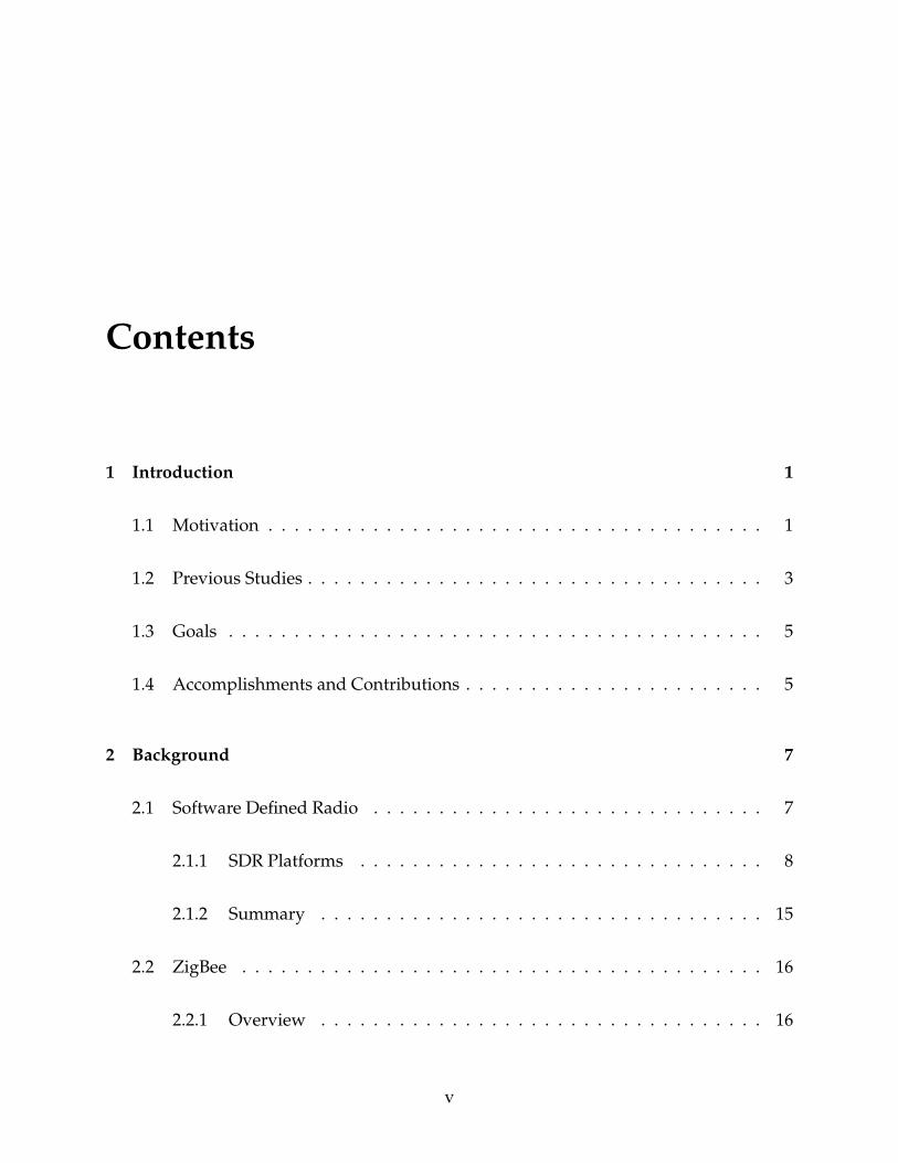
Contents
1 Introduction 1
1.1 Motivation . . . . . . . . . . . . . . . . . . . . . . . . . . . . . . . . . . . . . . 1
1.2 Previous Studies . . . . . . . . . . . . . . . . . . . . . . . . . . . . . . . . . . . 3
1.3 Goals . . . . . . . . . . . . . . . . . . . . . . . . . . . . . . . . . . . . . . . . . 5
1.4 Accomplishments and Contributions . . . . . . . . . . . . . . . . . . . . . . . 5
2 Background 7
2.1 Software Defined Radio . . . . . . . . . . . . . . . . . . . . . . . . . . . . . . 7
2.1.1 SDR Platforms . . . . . . . . . . . . . . . . . . . . . . . . . . . . . . . 8
2.1.2 Summary . . . . . . . . . . . . . . . . . . . . . . . . . . . . . . . . . . 15
2.2 ZigBee . . . . . . . . . . . . . . . . . . . . . . . . . . . . . . . . . . . . . . . . 16
2.2.1 Overview . . . . . . . . . . . . . . . . . . . . . . . . . . . . . . . . . . 16
v

2.2.2 IEEE 802.15.4 . . . . . . . . . . . . . . . . . . . . . . . . . . . . . . . . 17
2.3 Polyphase Filter-Bank Channelizer . . . . . . . . . . . . . . . . . . . . . . . . 21
2.4 USRP N210 . . . . . . . . . . . . . . . . . . . . . . . . . . . . . . . . . . . . . . 25
2.4.1 Signal Processing in FPGA of USRP N210 . . . . . . . . . . . . . . . . 26
3 Methodology and Implementation 32
3.1 IEEE 802.15.4 PHY on FPGA . . . . . . . . . . . . . . . . . . . . . . . . . . . . 32
3.1.1 Configuration . . . . . . . . . . . . . . . . . . . . . . . . . . . . . . . . 34
3.1.2 Transmitter . . . . . . . . . . . . . . . . . . . . . . . . . . . . . . . . . 35
3.1.3 Receiver . . . . . . . . . . . . . . . . . . . . . . . . . . . . . . . . . . . 39
3.2 Hybrid Multi-Channel IEEE 802.15.4 Receiver . . . . . . . . . . . . . . . . . 60
3.2.1 Configuration . . . . . . . . . . . . . . . . . . . . . . . . . . . . . . . . 60
3.2.2 Channelizer . . . . . . . . . . . . . . . . . . . . . . . . . . . . . . . . . 62
3.2.3 Energy Detector . . . . . . . . . . . . . . . . . . . . . . . . . . . . . . . 68
3.2.4 Resampler 4/5 . . . . . . . . . . . . . . . . . . . . . . . . . . . . . . . 68
3.2.5 Ethernet interface . . . . . . . . . . . . . . . . . . . . . . . . . . . . . . 70
4 Results 74
vi
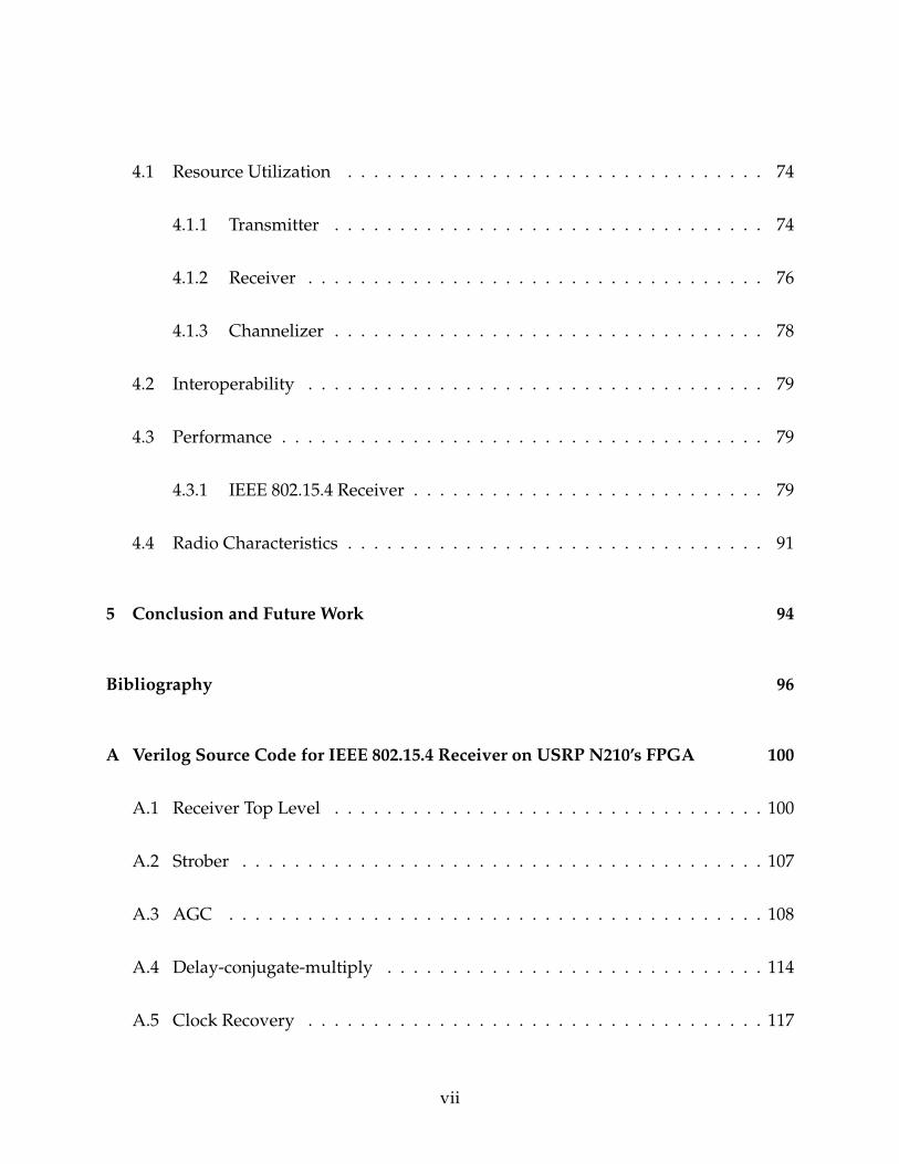
4.1 Resource Utilization . . . . . . . . . . . . . . . . . . . . . . . . . . . . . . . . 74
4.1.1 Transmitter . . . . . . . . . . . . . . . . . . . . . . . . . . . . . . . . . 74
4.1.2 Receiver . . . . . . . . . . . . . . . . . . . . . . . . . . . . . . . . . . . 76
4.1.3 Channelizer . . . . . . . . . . . . . . . . . . . . . . . . . . . . . . . . . 78
4.2 Interoperability . . . . . . . . . . . . . . . . . . . . . . . . . . . . . . . . . . . 79
4.3 Performance . . . . . . . . . . . . . . . . . . . . . . . . . . . . . . . . . . . . . 79
4.3.1 IEEE 802.15.4 Receiver . . . . . . . . . . . . . . . . . . . . . . . . . . . 79
4.4 Radio Characteristics . . . . . . . . . . . . . . . . . . . . . . . . . . . . . . . . 91
5 Conclusion and Future Work 94
Bibliography 96
A Verilog Source Code for IEEE 802.15.4 Receiver on USRP N210’s FPGA 100
A.1 Receiver Top Level . . . . . . . . . . . . . . . . . . . . . . . . . . . . . . . . . 100
A.2 Strober . . . . . . . . . . . . . . . . . . . . . . . . . . . . . . . . . . . . . . . . 107
A.3 AGC . . . . . . . . . . . . . . . . . . . . . . . . . . . . . . . . . . . . . . . . . 108
A.4 Delay-conjugate-multiply . . . . . . . . . . . . . . . . . . . . . . . . . . . . . 114
A.5 Clock Recovery . . . . . . . . . . . . . . . . . . . . . . . . . . . . . . . . . . . 117
vii
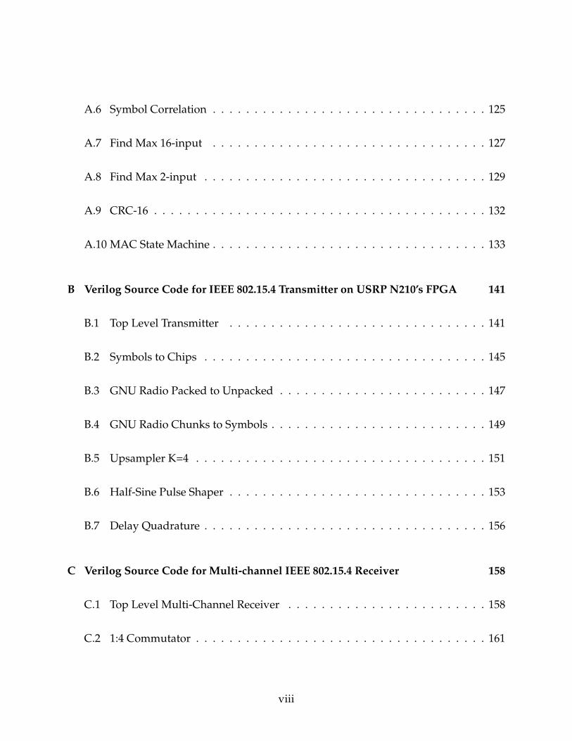
A.6 Symbol Correlation . . . . . . . . . . . . . . . . . . . . . . . . . . . . . . . . . 125
A.7 Find Max 16-input . . . . . . . . . . . . . . . . . . . . . . . . . . . . . . . . . 127
A.8 Find Max 2-input . . . . . . . . . . . . . . . . . . . . . . . . . . . . . . . . . . 129
A.9 CRC-16 . . . . . . . . . . . . . . . . . . . . . . . . . . . . . . . . . . . . . . . . 132
A.10 MAC State Machine . . . . . . . . . . . . . . . . . . . . . . . . . . . . . . . . . 133
B Verilog Source Code for IEEE 802.15.4 Transmitter on USRP N210’s FPGA 141
B.1 Top Level Transmitter . . . . . . . . . . . . . . . . . . . . . . . . . . . . . . . 141
B.2 Symbols to Chips . . . . . . . . . . . . . . . . . . . . . . . . . . . . . . . . . . 145
B.3 GNU Radio Packed to Unpacked . . . . . . . . . . . . . . . . . . . . . . . . . 147
B.4 GNU Radio Chunks to Symbols . . . . . . . . . . . . . . . . . . . . . . . . . . 149
B.5 Upsampler K=4 . . . . . . . . . . . . . . . . . . . . . . . . . . . . . . . . . . . 151
B.6 Half-Sine Pulse Shaper . . . . . . . . . . . . . . . . . . . . . . . . . . . . . . . 153
B.7 Delay Quadrature . . . . . . . . . . . . . . . . . . . . . . . . . . . . . . . . . . 156
C Verilog Source Code for Multi-channel IEEE 802.15.4 Receiver 158
C.1 Top Level Multi-Channel Receiver . . . . . . . . . . . . . . . . . . . . . . . . 158
C.2 1:4 Commutator . . . . . . . . . . . . . . . . . . . . . . . . . . . . . . . . . . . 161
viii
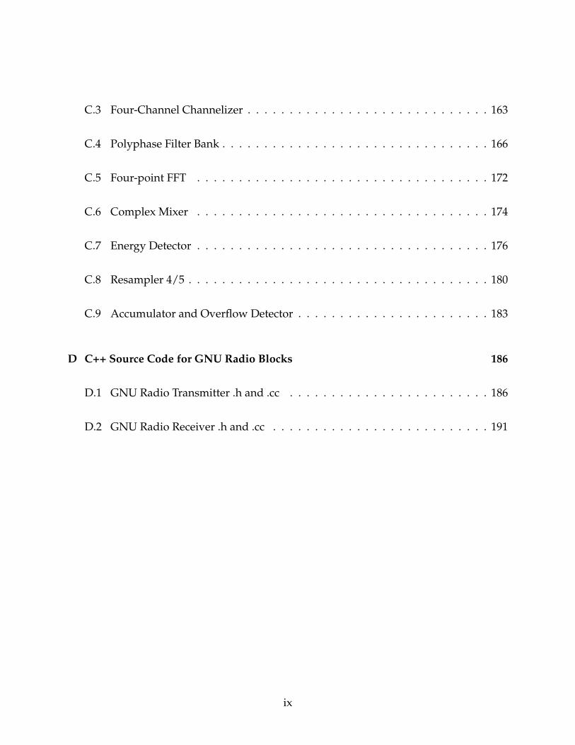
C.3 Four-Channel Channelizer . . . . . . . . . . . . . . . . . . . . . . . . . . . . . 163
C.4 Polyphase Filter Bank . . . . . . . . . . . . . . . . . . . . . . . . . . . . . . . . 166
C.5 Four-point FFT . . . . . . . . . . . . . . . . . . . . . . . . . . . . . . . . . . . 172
C.6 Complex Mixer . . . . . . . . . . . . . . . . . . . . . . . . . . . . . . . . . . . 174
C.7 Energy Detector . . . . . . . . . . . . . . . . . . . . . . . . . . . . . . . . . . . 176
C.8 Resampler 4/5 . . . . . . . . . . . . . . . . . . . . . . . . . . . . . . . . . . . . 180
C.9 Accumulator and Overflow Detector . . . . . . . . . . . . . . . . . . . . . . . 183
D C++ Source Code for GNU Radio Blocks 186
D.1 GNU Radio Transmitter .h and .cc . . . . . . . . . . . . . . . . . . . . . . . . 186
D.2 GNU Radio Receiver .h and .cc . . . . . . . . . . . . . . . . . . . . . . . . . . 191
ix

List of Abbreviations
ASIC Application-Specific Integrated Circuit
ASK Amplitude-Shift Keying
CIC Cascaded Integrator-Comb
CLB Configurable Logic Block
CRC Cyclic Redundancy Check
CSMA-CA Carrier Sense Multiple Access Collision Avoidance
DAC Digital-to-Analog Converter
DFT Discrete Fourier Transform
DSP Digital Signal Processor
DSSS Direct Sequence Spread Spectrum
FFT Fast Fourier Transform
x
FIR Finite Impulse Response
FPGA Field-Programmable Gate Array
GPP General Purpose Processor
HDL Hardware Description Language
ISM Industrial, Scientific and Medical
LUT Look-Up Table
MAC Media Access Control
MAC multiply-accumulate
MSK Minimum-Shift Keying
O-QPSK Offset Quadrature Phase-Shift Keying
PHR PHY Header
PHY Physical Layer
PN Pseudo-random Noise
PPDU PHY Protocol Data Unit
PSDU Physical Layer Service Data Unit
RTL Register-Transfer Level
xi

SDR Software Defined Radio
SFD Start of Frame Delimiter
SHR Synchronization Header
SOC System on Chip
SVD Singular Value Decomposition
UDP User Datagram Protocol
USRP Universal Software Radio Peripheral
VITA VMEbus International Trade Association
VRT VITA Radio Transport
WPAN Wireless Personal Area Network
xii

List of Figures
2.1 Ideal Software Defined Radio . . . . . . . . . . . . . . . . . . . . . . . . . . . 8
2.2 IEEE 802.15.4 Data Frame [1] . . . . . . . . . . . . . . . . . . . . . . . . . . . 18
2.3 O-QPSK Chip Offset [1] . . . . . . . . . . . . . . . . . . . . . . . . . . . . . . 21
2.4 Polyphase Channelizer . . . . . . . . . . . . . . . . . . . . . . . . . . . . . . . 22
2.5 Single Channel M-to-1 Resampler . . . . . . . . . . . . . . . . . . . . . . . . . 23
2.6 Input to Eight-Channel Channelizer . . . . . . . . . . . . . . . . . . . . . . . 24
2.7 Output of Each Channel . . . . . . . . . . . . . . . . . . . . . . . . . . . . . . 25
2.8 SOC in USRP’s FPGA . . . . . . . . . . . . . . . . . . . . . . . . . . . . . . . . 27
2.9 Transmit Signal Processing Chain . . . . . . . . . . . . . . . . . . . . . . . . . 27
2.10 Time-Domain Plot of First Half-Band Filter . . . . . . . . . . . . . . . . . . . 28
2.11 Time-Domain Plot of Second Half-Band Filter . . . . . . . . . . . . . . . . . . 29
2.12 Frequency Response of Two Halfband Filters . . . . . . . . . . . . . . . . . . 29
xiii
2.13 CIC Interpolator in USRP N210 . . . . . . . . . . . . . . . . . . . . . . . . . . 30
2.14 Frequency Response of CIC Interpolator . . . . . . . . . . . . . . . . . . . . . 30
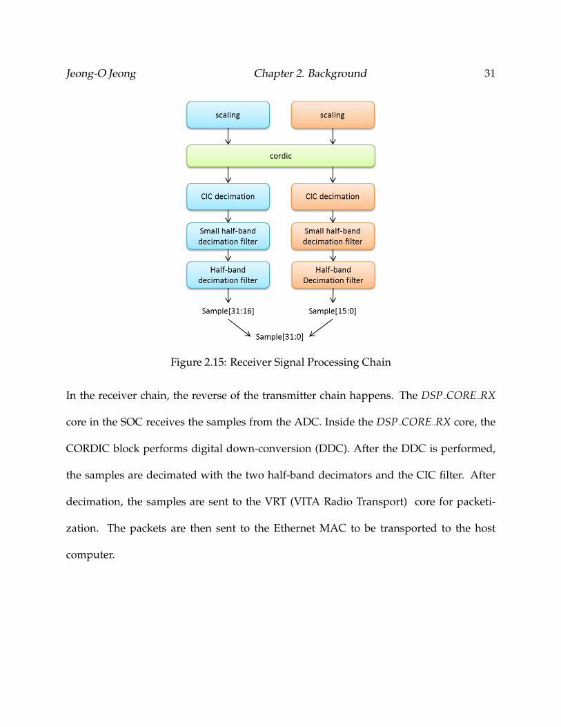
2.15 Receiver Signal Processing Chain . . . . . . . . . . . . . . . . . . . . . . . . . 31
3.1 Two Paths Explored in FPGA Implementation . . . . . . . . . . . . . . . . . 33
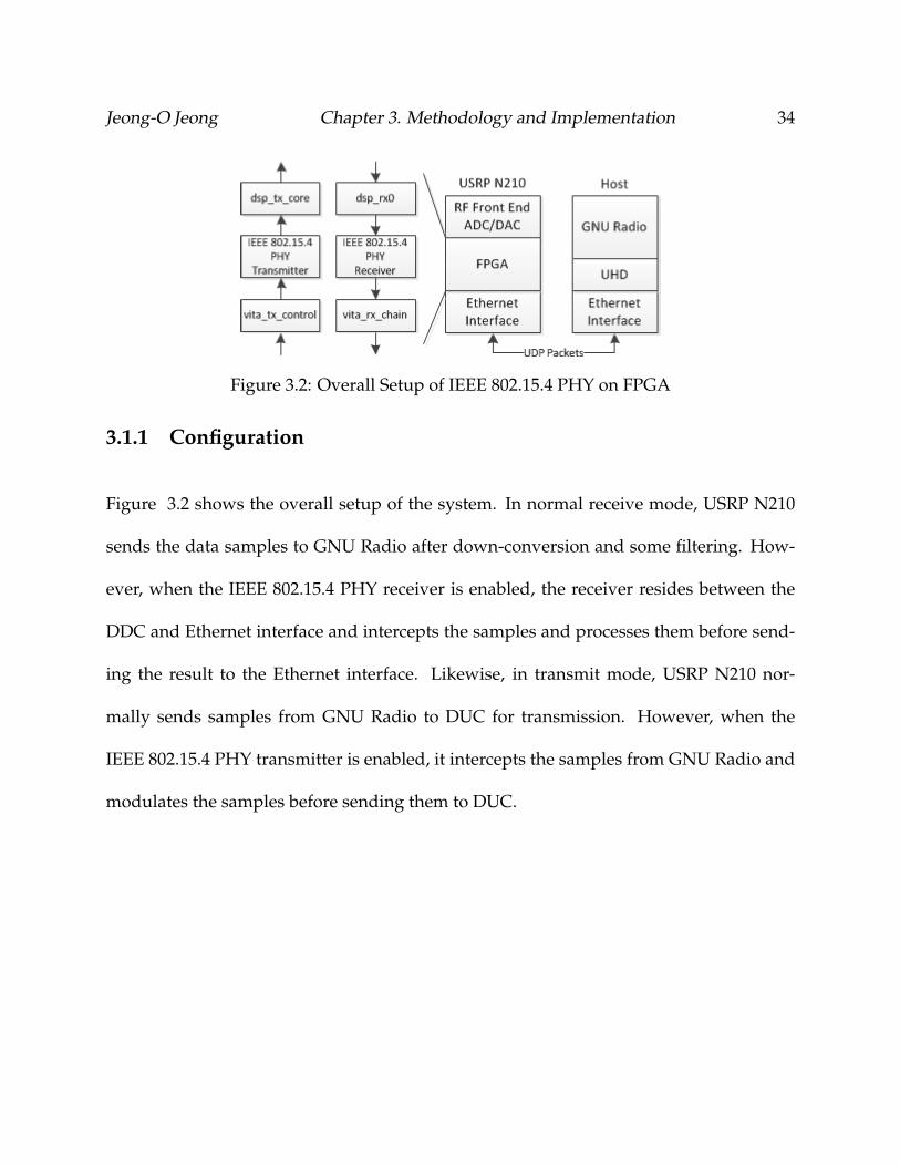
3.2 Overall Setup of IEEE 802.15.4 PHY on FPGA . . . . . . . . . . . . . . . . . . 34
3.3 Overall Transmitter Chain . . . . . . . . . . . . . . . . . . . . . . . . . . . . . 35
3.4 Simulation of O-QPSK at Baseband . . . . . . . . . . . . . . . . . . . . . . . . 35
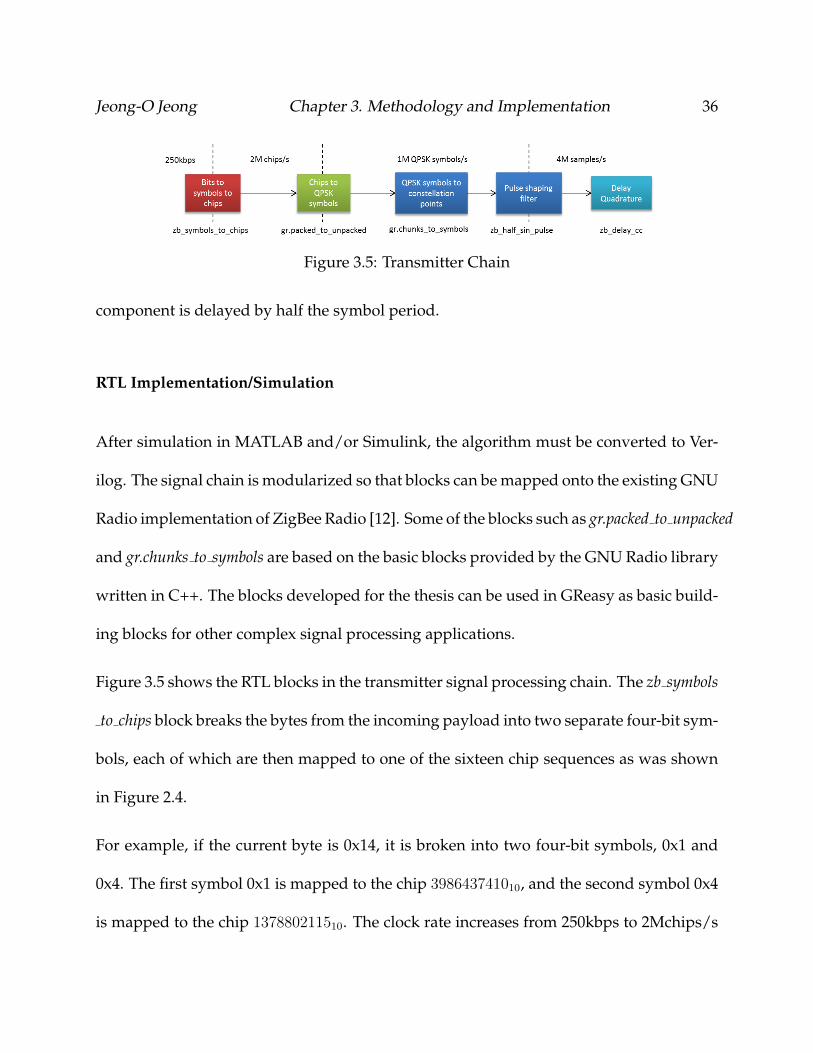
3.5 Transmitter Chain . . . . . . . . . . . . . . . . . . . . . . . . . . . . . . . . . . 36
3.6 ModelSim simulation of transmitted signal . . . . . . . . . . . . . . . . . . . 38
3.7 Transmitter module inside USRP’s FPGA . . . . . . . . . . . . . . . . . . . . 39
3.8 Chipscope showing interpolated in-phase waveform of O-QPSK . . . . . . . 40
3.9 Overall receiver algorithm . . . . . . . . . . . . . . . . . . . . . . . . . . . . . 40
3.10 AGC Structure . . . . . . . . . . . . . . . . . . . . . . . . . . . . . . . . . . . . 41
3.11 Delay-conjugate-multiply . . . . . . . . . . . . . . . . . . . . . . . . . . . . . 42
3.12 Output of delay-conjugate-multiply . . . . . . . . . . . . . . . . . . . . . . . 42
3.13 Clock Recovery Block Structure . . . . . . . . . . . . . . . . . . . . . . . . . . 43
3.14 Comparison of Sampled Chips With and Without Clock Recovery . . . . . . 43
xiv
3.15 Preamble and SFD correlations . . . . . . . . . . . . . . . . . . . . . . . . . . 44
3.16 BER Simulation of Soft vs. Hard Correlations . . . . . . . . . . . . . . . . . . 47
3.17 Packet Detection Rate Simulation of Soft vs. Hard Correlations . . . . . . . . 47
3.18 Output of delay-conjugate-multiply with frequency offset of 20 KHz . . . . 48
3.19 Frequency Offset Estimation . . . . . . . . . . . . . . . . . . . . . . . . . . . . 51
3.20 Delay-conjugate-multiply Block in Simulink . . . . . . . . . . . . . . . . . . 51
3.21 Complex Mulitply Block in Simulink . . . . . . . . . . . . . . . . . . . . . . . 52
3.22 Black Box wrapper for a simple MAC processing . . . . . . . . . . . . . . . . 52
3.23 Output of CORDIC atan without AGC . . . . . . . . . . . . . . . . . . . . . . 53
3.24 Output of CORDIC atan with AGC . . . . . . . . . . . . . . . . . . . . . . . . 54
3.25 ModelSim Simulation Showing Preamble and SFD Corrleations . . . . . . . 55
3.26 CRC-16 . . . . . . . . . . . . . . . . . . . . . . . . . . . . . . . . . . . . . . . . 55
3.27 State machine for MAC layer . . . . . . . . . . . . . . . . . . . . . . . . . . . 56
3.28 Receiver module inside USRP’s FPGA . . . . . . . . . . . . . . . . . . . . . . 57
3.29 GNU Radio companion view of ZigBee RX . . . . . . . . . . . . . . . . . . . 59
3.30 Modified UHD USRP Source Block . . . . . . . . . . . . . . . . . . . . . . . . 59
3.31 Control Chain in Modifying Registers Inside FPGA from GNU Radio . . . . 61
xv
3.32 System Configuration of Hybrid Multi-Channel IEEE 802.15.4 Receiver . . . 62
3.33 Channelizer 4:1 . . . . . . . . . . . . . . . . . . . . . . . . . . . . . . . . . . . 63
3.34 Prototype Lowpass Filter . . . . . . . . . . . . . . . . . . . . . . . . . . . . . . 64
3.35 Input to Four-Channel Channelizer . . . . . . . . . . . . . . . . . . . . . . . . 64
3.36 Output of Four-Channel Channelizer . . . . . . . . . . . . . . . . . . . . . . . 65
3.37 Filter with Real Coefficients . . . . . . . . . . . . . . . . . . . . . . . . . . . . 65
3.38 Filter with Complex Coefficients . . . . . . . . . . . . . . . . . . . . . . . . . 65
3.39 Energy Detector . . . . . . . . . . . . . . . . . . . . . . . . . . . . . . . . . . . 68
3.40 Resampler 4/5 . . . . . . . . . . . . . . . . . . . . . . . . . . . . . . . . . . . . 69
3.41 Resampler 4/5 Simulation . . . . . . . . . . . . . . . . . . . . . . . . . . . . . 69
3.42 Flow of Data and Control Packets . . . . . . . . . . . . . . . . . . . . . . . . . 70
3.43 Ethernet interface in XUPV5 . . . . . . . . . . . . . . . . . . . . . . . . . . . . 72
3.44 Frames at Different OSI Layers . . . . . . . . . . . . . . . . . . . . . . . . . . 72
4.1 Message from FPGA received by Xbee console . . . . . . . . . . . . . . . . . 80
4.2 Chip Error Rate Simulation . . . . . . . . . . . . . . . . . . . . . . . . . . . . 81
4.3 BER Simulation . . . . . . . . . . . . . . . . . . . . . . . . . . . . . . . . . . . 82
4.4 Received Packets in Time Domain . . . . . . . . . . . . . . . . . . . . . . . . 83
xvi

4.5 Percentages of Packets Detected . . . . . . . . . . . . . . . . . . . . . . . . . . 86
4.6 Packet Error Rate . . . . . . . . . . . . . . . . . . . . . . . . . . . . . . . . . . 86
4.7 Bit Error Rate . . . . . . . . . . . . . . . . . . . . . . . . . . . . . . . . . . . . 87
4.8 Output of Inverse Tangent with Correct Sign . . . . . . . . . . . . . . . . . . 88
4.9 Output of Inverse Tangent with Mismatched Sign . . . . . . . . . . . . . . . 89
4.10 Output of Inverse Tangent with Increased CORDIC Iterations . . . . . . . . 89
4.11 Packet Detection Rate with Varying Word Length . . . . . . . . . . . . . . . 90
4.12 Spectral Mask of IEEE 802.15.4 transmitted using USRP N210 FPGA . . . . 92
4.13 Center Frequency of IEEE 802.15.4 Signal from USRP N210 FPGA . . . . . . 93
4.14 Occupied Bandwidth . . . . . . . . . . . . . . . . . . . . . . . . . . . . . . . . 93
4.15 O-QPSK Constellation . . . . . . . . . . . . . . . . . . . . . . . . . . . . . . . 93
xvii
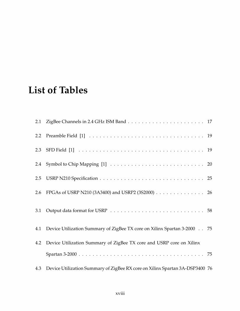
List of Tables
2.1 ZigBee Channels in 2.4 GHz ISM Band . . . . . . . . . . . . . . . . . . . . . . 17
2.2 Preamble Field [1] . . . . . . . . . . . . . . . . . . . . . . . . . . . . . . . . . 19
2.3 SFD Field [1] . . . . . . . . . . . . . . . . . . . . . . . . . . . . . . . . . . . . 19
2.4 Symbol to Chip Mapping [1] . . . . . . . . . . . . . . . . . . . . . . . . . . . 20
2.5 USRP N210 Specification . . . . . . . . . . . . . . . . . . . . . . . . . . . . . . 25
2.6 FPGAs of USRP N210 (3A3400) and USRP2 (3S2000) . . . . . . . . . . . . . . 26
3.1 Output data format for USRP . . . . . . . . . . . . . . . . . . . . . . . . . . . 58
4.1 Device Utilization Summary of ZigBee TX core on Xilinx Spartan 3-2000 . . 75
4.2 Device Utilization Summary of ZigBee TX core and USRP core on Xilinx
Spartan 3-2000 . . . . . . . . . . . . . . . . . . . . . . . . . . . . . . . . . . . . 75
4.3 Device Utilization Summary of ZigBee RX core on Xilinx Spartan 3A-DSP3400 76
xviii
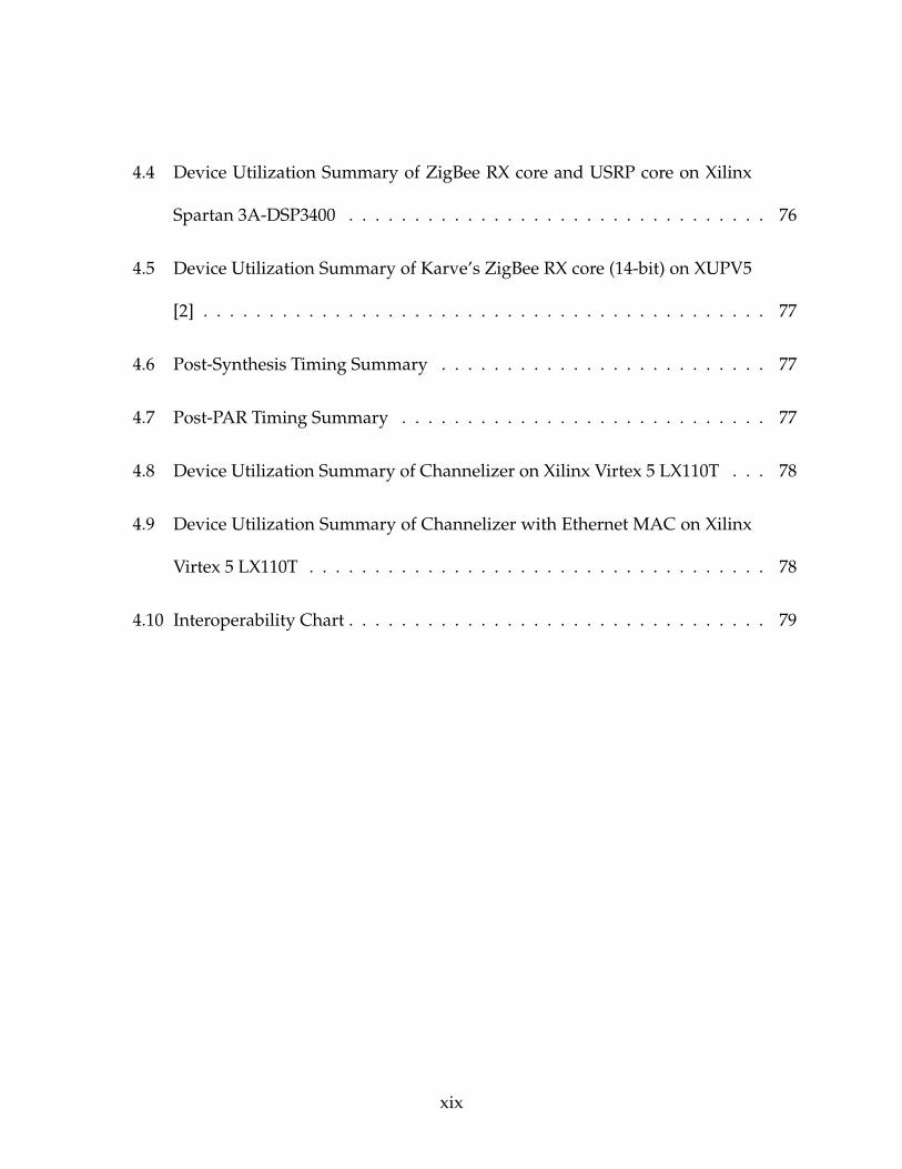
4.4 Device Utilization Summary of ZigBee RX core and USRP core on Xilinx
Spartan 3A-DSP3400 . . . . . . . . . . . . . . . . . . . . . . . . . . . . . . . . 76
4.5 Device Utilization Summary of Karve’s ZigBee RX core (14-bit) on XUPV5
[2] . . . . . . . . . . . . . . . . . . . . . . . . . . . . . . . . . . . . . . . . . . . 77
4.6 Post-Synthesis Timing Summary . . . . . . . . . . . . . . . . . . . . . . . . . 77
4.7 Post-PAR Timing Summary . . . . . . . . . . . . . . . . . . . . . . . . . . . . 77
4.8 Device Utilization Summary of Channelizer on Xilinx Virtex 5 LX110T . . . 78
4.9 Device Utilization Summary of Channelizer with Ethernet MAC on Xilinx
Virtex 5 LX110T . . . . . . . . . . . . . . . . . . . . . . . . . . . . . . . . . . . 78
4.10 Interoperability Chart . . . . . . . . . . . . . . . . . . . . . . . . . . . . . . . . 79
xix
Chapter 1
Introduction
1.1 Motivation
Software Defined Radio (SDR) attempts to leverage the flexibility of software or recon-
figurable hardware to implement flexible radios that can easily switch to different wave-
forms and standards. This is achieved by migrating most of the signal processing tradi-
tionally implemented on hardware onto software. By implementing the signal processing
region with software, the matter of reconfiguring the system is simply loading a different
image, which can be done even in real-time. The most common platforms on which SDR
is implemented are GPP (general purpose processor), DSP (digital signal processor),and
FPGA (field-programmable gate array). Each of these platforms has its own advantages
and disadvantages. Although GPPs are relatively easy to program, test, and verify, they
1
Jeong-O Jeong Chapter 1. Introduction 2
are often not well-suited for parallel, signal-processing intensive, or real-time constrained
operations. DSPs are optimized for certain signal processing tasks, but they are harder to
program than GPPs and not optimized for parallel computations. FPGAs are well-suited
for parallel and signal-processing intensive computations, but they are much harder to
program and verify. However, many high-level tools such as Simulink and ImpulseC
are available to facilitate the programming of FPGA. These tools allow engineers to de-
scribe the algorithm at high-level that can be automatically converted to HDL (Hardware
Description Language) to be implemented on the FPGA.
As mentioned, GPPs and DSPs are not the best platforms on which signal-processing in-
tensive algorithms can be implemented. Processing power necessary for even one of the
simplest wireless protocols such as IEEE 802.15.4 can be too demanding for GPP unless
it is a very high-performance GPP. Even with a high-performance GPP, signal process-
ing required for IEEE 802.15.4 consumes most of CPU cycles. It can be seen that wide-
band wireless protocols such as IEEE 802.11a, which has 20 MHz of bandwidth and com-
plex modulation scheme such as 52-subcarrier OFDM will be too demanding for GPPs.
However, FPGAs, with their ability to perform computations in parallel, support high
throughput and high sampling rate that GPPs or DSPs are not able to achieve. ASICs
are a popular platform for implementing high-performance protocols, but they have very
low re-configurability. With its software-like configurability, FPGAs bring significant re-
duction in NRE (non-recurring engineering) costs. Once a prototype is built and fault
is found in the design, FPGAs can be reconfigured with a modified bit-stream and can
Jeong-O Jeong Chapter 1. Introduction 3
be tested again, whereas ASICs need to be re-spun at a very high-cost, often in millions
of dollars [3]. Because FPGAs are high-performance like ASICs and flexible like GPPs
and DSPs, they are an ideal platform on which prototype wireless protocols can be built
and tested. Additionally, the partial reconfiguration ability of FPGA allows it to recon-
figure itself in real-time, which unlocks the SDR’s promises of concurrent multi-protocol
operation.
1.2 Previous Studies
Many implementations of SDR have been done on FPGAs. At Virginia Tech, Charles Irick
from Configurable Computing Lab developed an SDR framework which improves upon
the GNU Radio framework by allowing an auxiliary Virtex-5 FPGA. In the enhanced
GNU Radio framework, a software block representing the auxiliary FPGA controls the
dataflow within the software environment. A single high-level software description of
GNU Radio and FPGA leaves the mixture of software blocks and the FPGA block trans-
parent to the programmer [4]. More recently, Richard Stroop from the same lab has ex-
tended Irick’s work to develop a framework called GReasy (GNU Radio Easy). Whereas
Irick’s work only used a USRP2 as RF front-end and a single auxiliary FPGA, GReasy has
successfully worked with not only USRP2 but also a 3.6GSPS ADC as an RF front-end.
It has also interfaced with four auxiliary FPGAs for distributed FPGA processing. More
importantly, the framework allows rapid reconfiguration of the FPGA by placing and
Jeong-O Jeong Chapter 1. Introduction 4
routing pre-compiled modules. Thus, GReasy presents the user interface where FPGA
blocks can be as easily placed and rearranged as software blocks, and the underlying
mechanism for compiling the FPGA remains transparent to the user.
In Karve’s Master’s thesis, the enhanced GNURadio framework developed by Irick was
used to implement a ZigBee receiver. The O-QPSK demodulator was implemented on
the FPGA. An off-the-shelf ZigBee-compliant solution called XBee was used to transmit
packets, which were then received by a ZigBee receiver developed with the framework
for verification of interoperability [2].
Implementations of SDR based on other platforms such as GPPs and DSPs are also avail-
able. An SDR platform known as SORA is developed on commodity PC architectures.
The platform consists of a radio-front end, a radio control board, and a PCIe bus to the
CPU cores. Researches have developed full IEEE 802.11 a/b/g PHY and MAC layers on
the SORA platform and successfully interoperated with commercial IEEE 802.11 a/b/g
devices. It was possible to implement such a complex standard by introducing optimiza-
tions such as replacing complex computations with extensive use of LUTs (Look-Up Ta-
bles) in L2 cache and use of SIMD (Single Instruction Multiple Data) instruction sets [5].
Other SDR platforms are based on custom reconfigurable hardware. The AsAP2 (Asyn-
chronous Array of Simple Processors) platform from University of California Davis is
composed of an array of 164 simple processors and Viterbi and FFT accelerators. Each
processor has own instruction and data memory as well as arithmetic and logic unit. Us-
ing this platform, they were able to implement a complete IEEE 802.11a baseband receiver

Jeong-O Jeong Chapter 1. Introduction 5
[6].
1.3 Goals
The following list outlines the goals for the thesis.
• To implement IEEE 802.15.4 PHY on Xilinx Spartan 3A-DSP of USRP N210
• To implement a channelizer on an external Virtex 5 FPGA
• To interface GNU Radio and the external Virtex 5 FPGA for hybrid implementations
• To compare performance between GNU Radio and FPGA implementations of IEEE
802.15.4 PHY
• To lay the groundwork for more complex wireless communication protocols and
applications to be implemented on FPGA with USRP N210 as an RF front end
• To develop open-source IP cores to be freely used in other SDR projects
1.4 Accomplishments and Contributions
The main accomplishment of this thesis is the implementation of the IEEE 802.15.4 PHY
on the FPGA. The FPGA implementation was able to successfully inter-operate with a
commercially available, standard-compliant ZigBee module as well as an open-source
Jeong-O Jeong Chapter 1. Introduction 6
GNU Radio implementation. Secondly, the interfacing between USRP N210, an external
FPGA and GNU Radio with UHD (Universal Hardware Driver) has been implemented.
This enables the hybrid implementation of a waveform where a more complex signal pro-
cessing task such as channelization is performed on the external FPGA, while a simpler
task such as demodulation of an IEEE 802.15.4 packet is performed on GNU Radio. Fi-
nally, numerous FPGA blocks developed in the course of this thesis work have been made
available to Configurable Computing Lab at Virginia Tech for the GReasy project.
Chapter 2
Background
2.1 Software Defined Radio
The term Software Defined Radio, coined by Joe Mitola in 1991, describes a radio whose
physical layer is implemented mostly in software. It is a radio “whose physical layer
behavior can be significantly altered through changes to its software” [7]. Common
platforms for SDR include General Purpose Processors (GPP), Digital Signal Processors
(DSP), Field Programmable Gate Arrays (FPGA), and recently even Graphics Processing
Unit (GPU). Traditionally, radios are implemented in hardware, which makes it difficult
to modify or upgrade after deployment. However, the software-defined nature of SDRs
allows ease of modification and flexibility not found in hardware-defined radios. Because
of its flexibility, SDRs can be prepared for “proliferation of wireless standards in the fu-
7
Jeong-O Jeong Chapter 2. Background 8
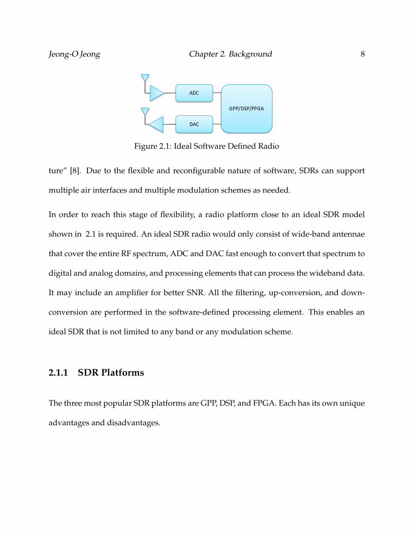
Figure 2.1: Ideal Software Defined Radio
ture” [8]. Due to the flexible and reconfigurable nature of software, SDRs can support
multiple air interfaces and multiple modulation schemes as needed.
In order to reach this stage of flexibility, a radio platform close to an ideal SDR model
shown in 2.1 is required. An ideal SDR radio would only consist of wide-band antennae
that cover the entire RF spectrum, ADC and DAC fast enough to convert that spectrum to
digital and analog domains, and processing elements that can process the wideband data.
It may include an amplifier for better SNR. All the filtering, up-conversion, and down-
conversion are performed in the software-defined processing element. This enables an
ideal SDR that is not limited to any band or any modulation scheme.
2.1.1 SDR Platforms
The three most popular SDR platforms are GPP, DSP, and FPGA. Each has its own unique
advantages and disadvantages.
Jeong-O Jeong Chapter 2. Background 9
GPP (General Purpose Processor)
GPP is a processing unit used for a variety of purposes such as fixed and floating point
arithmetic, memory interface, and general input and output. It supports multiple high-
level programming languages, and therefore it is the most flexible and easiest to program.
However, GPPs generally do not perform computation in parallel and are not optimized
for arithmetic operations. For example, the multiply-add operation, the most common
operation in signal processing, is not supported in hardware in GPPs.
However, modern microprocessors have started to employ different ways of parallelism
to improve DSP and graphics operations. One example is hyperthreading in Intel mi-
croprocessors. Hyperthreading allows a single core to act as two logical cores that can
execute threads in parallel. Each logical core has its own processor architectural state and
shares the execution resources of the physical core. This results in a performance gain of
30 percent when executing multithreaded applications compared to a processor without
hyperthreading [9].
Another example of parallelism is the SIMD (single instruction multiple data) technology,
known as SSE (Streaming SIMD Extensions) in Intel and 3DNow! in AMD processors. It
allows a single instruction to be applied on multiple data simultaneously. This is more
efficient than the traditional SISD (single instruction single data) where a single instruc-
tion is executed on single data at a time. FFTW, the fastest software implementation of
the FFT algorithm, takes advantage of SIMD to achieve its title [10].
Jeong-O Jeong Chapter 2. Background 10
The most well-known and established SDR platform for GPP is an open-source software
called GNU Radio. It is a software development platform that enables researchers to build
software radios from a library of signal processing blocks. While the signal processing
blocks are written in C++, the glue logic that connects the blocks is written in Python.
Users can also develop their own custom signal processing blocks for their application.
Like FFTW, GNU Radio also takes advantage of SIMD with its VOLK (vector-optimized
library of kernels) library. The library consists of vector operations that provide much im-
provement in performance. For example, a function called volk 32fc multiply aligned16(c,
a, b, N) can perform vector multiplication of two vectors with N items. Without SIMD, the
operation would be performed using a standard for-loop that multiplies each vector ele-
ment, but SIMD allows simultaneous multiplication of the vector elements. Rondeau re-
ports ten percent improvement in speed when using the function in the FFT filters where
large number of multiplies may be required [11].
An example of a wireless standard implemented in GNU Radio is the ZigBee PHY im-
plementation by Thomas Schmid from UCLA [12]. The signal processing is done on the
general purpose processor with the USRP (Universal Software Radio Peripheral) as the
RF front-end. The implementation was verified with a commercially available ZigBee ra-
dio compliant with the IEEE 802.15.4 standard. Because of issues such as high latency
in GNU Radio, the full protocol stack could not be implemented, but only the physical
layer was implemented. The physical layer implemented in this project was 2450 MHz
O-QPSK PHY.
Jeong-O Jeong Chapter 2. Background 11
Schmid reports that even the high-performance machine they used, a dual Pentium IV, 2.8
GHz with hyperthreading and 4 GB of RAM, could not decode a constant stream of data
from the USRP. To measure its performance, the throughput of GNU Radio implementa-
tion was measured. At 45 bytes per message, including both the MAC layer payload of
27 bytes and extra bytes at the PHY layer, the GNU Radio implementation could decode
slightly above 200 messages per second.
DSP (Digital Signal Processor)
DSP is a microprocessor optimized for mathematical operations, specifically multiply-
accumulate (MAC) functions. Unlike GPPs which use Von Nuemann architecture, DSPs
use the Harvard architecture. While the Von Nuemann architecture provides a single
bus to fetch both instruction and data from memory, the Harvard architecture provides
separate buses for instructions and data. This allows instructions and data to be accessed
at the same time for faster computation.
Modern DSPs also employ the VLIW (very long instruction word) architecture. VLIW
allows the processor to run multiple independent instructions in a single clock cycle, thus
increasing parallelism. DSPs with VLIW provides a performance gain of 1.8 to 2.8 times
over traditional DSPs without VLIW [13].
The most distinguishing feature of DSPs is the hardware MAC unit. It performs multiply-
accumulate operation which forms the basis of essential DSP operations such as FIR fil-
Jeong-O Jeong Chapter 2. Background 12
tering, correlations, and FFTs. With specialized MAC blocks, DSPs can perform multiply-
accumulate in one or two clock cycles, while it can take multiple clock cycles in GPPs
[14].
However, even with dedicated MAC units, data-intensive processes such as Viterbi en-
coding and decoding are difficult to accelerate. Some DSP chips provide dedicated hardware-
based co-processors such as Viterbi-decoder and turbo decoder, but they cannot be cus-
tomized to specific design needs [15].
Because of special instruction sets and specialized architectural features, DSPs are usually
programmed in low level languages such as assembly and C.
FPGA (Field-Programmable Gate Array)
FPGA is a reconfigurable hardware consisting of configurable logic blocks (CLBs) and
macro blocks connected via programmable interconnects. Xilinx Spartan-3A DSP FPGA
targeted for this thesis consists of four types of macro blocks in addition to CLBs: XtremeDSP
DSP48A Slice, Block RAM, Input/Output Blocks, and Digital Clock Manager.
CLBs usually consist of look-up tables, flip-flops, and multiplexers, but they can vary
among different FPGA devices. Xilinx Spartan-3A DSP FPGA has four slices in each
CLB. A slice consists of two LUTs (Look-Up Tables) , two flip-flops, two multiplexers,
and a carry-chain. Although CLBs can be used to implement multipliers and adders,
Spartan-3A FPGA provides XtremeDSP DSP48A slices that are dedicated for 18-bit by 18-

Jeong-O Jeong Chapter 2. Background 13
bit multiplication and 48-bit accumulation for MAC (multiply-accumulate) operations.
The DSP48A slices are ideal for implementing FIR filters which require adder, multiplier,
and storage elements. They can be highly pipelined to provide maximum clock frequen-
cies of 250 MHz.
Virtex 5 LX110T, the other FPGA targeted for this thesis, is a more advanced FPGA than
Spartan 3A-DSP. Each slice contains four LUTs, four flipflops, multiplexers, and carry
logic. The FPGA also has DSP48E slices which supports 25-bit by 18-bit multiplication,
48-bit adder, and accumulator. With maximum pipelining the DSP48E slices can operate
at the maximum frequency of 550 MHz [16].
y[n] =N−1∑i=0
x[n− i]h[i] (2.1)
When performing FIR (Finite Impulse Response) filtering shown in 2.1, DSP48E slices
can be arranged in multiple ways to trade-off speed and resource usage. The Single-
Multiplier MACC FIR Filter structure uses the least number of DSP48 slices but has the
lowest throughput. This structure performs multiply and accumulate on a pair of input
sample and filter coefficient at a time. Thus, it takes N clock cycles to produce a single
output for a N-tap filter. The Parallel FIR Filter structure uses N DSP48 slices to perform
simultaneous multiplication of N coefficients and N respective input samples and accu-
mulate the results. Thus, it takes a single clock cycle to produce a new output sample.
Therefore, the Parallel FIR structure has the highest throughput but uses the most num-
Jeong-O Jeong Chapter 2. Background 14
ber of DSP48 slices. The Semi-Parallel FIR Filter structure forms a hybrid between the two
structures to obtain a higher throughput than the Single-Multiplier structure but uses less
slices than the Parallel structure.
In addition to FIR filtering, other signal processing operations lend themselves well to
FPGA implementation. For example, taking singular value decomposition (SVD) , shown
in 2.2, of a matrix is a common operation in MIMO, radar, or image processing applica-
tions.
M = UΣV ∗ (2.2)
It is a very computationally intensive process that requires a large number of clock cycles
in sequential processors, but the algorithm to produce SVD can be parallelized to be sped
up greatly in FPGAs. One well-known systolic array implementation of SVD by Brent
can compute SVD in O(n log n) time using O(n2) processing elements [17]. AccelChip
reports a factor of 50 times increase in speed up with FPGA fixed-point implementation
of SVD of an 8x8 matrix compared to floating-point implementation done in a DSP chip
TI TMS320C67x [18].
Another advantage of FPGA over other platforms is that it is easy to trade-off between
speed and resource usage since the hardware is highly configurable. If the design takes up
too much resource, the design can be easily modified to be more resource-efficient at the
penalty of decrease in speed. On the other hand, if there is plenty of resource available,
Jeong-O Jeong Chapter 2. Background 15
the design can be fully parallelized to achieve maximum speed.
Since it is easily reconfigurable, FPGA can also be a great platform for prototyping a final
ASIC design. Once the design is finalized and HDL (Hardware Description Language) is
written for FPGA, it is often easy to port to ASIC for final production.
2.1.2 Summary
The three most common SDR platforms have been reviewed. Each platform has its own
advantages and disadvantages. GPPs are the easiest to program, test, and verify, but they
are often too slow to perform complex computations at high sample rates. With dedicated
MAC units, DSPs are better suited for signal processing than GPPs, but they too reach the
performance limit as the complexity of the application increases. FPGAs can meet per-
formance requirement needed for high bandwidth applications. However, they are often
much harder to program, test, and verify than the other two platforms. Fortunately, re-
cent developments in high-level tools such as Simulink and ImpulseC enable algorithm
developers to program FPGAs more easily. Also, tools such as AutoESL’s AutoPilot and
Synopsys Synphony C Compiler make it easy for DSP software engineers to convert their
high-level code in C/C++ to RTL (Register-Transfer-Level). These tools have reportedly
been able to achieve comparable resource utilization as manually written RTL code [19].
FPGAs may also be almost as energy efficient as DSPs when considering highly complex
signal processing applications. Since a large portion of DSP’s circuitry is dedicated to
Jeong-O Jeong Chapter 2. Background 16
data transfer, the overall energy consumption per computation of FPGA may be better
than that of DSP for some applications [20]. A hybrid approach where complex signal
processing is partitioned to FPGA while control-type operation is partitioned to micro-
processors maybe the best approach. In this thesis, such hybrid implementations of SDR
will be explored.
2.2 ZigBee
2.2.1 Overview
ZigBee is a LR-WPAN (Low Rate-Wireless Personal Area Network) standard commonly
used for home control applications and wireless sensor networks. The ZigBee standard
defines the application, security, and network layers of the protocol stack, while the phys-
ical (PHY) and medium access control (MAC) layers of the standard are based on IEEE
802.15.4. The standard specifies the maximum data rate to be 250kbps and the maximum
range to be 100m. Because of its low data rate and simple architecture, it is low cost
and consumes less power compared to other WPAN protocols such as Bluetooth. ZigBee
devices can last as long as five years on a pair of AA batteries [21].
The network layer of ZigBee supports different types of network topologies such as star,
tree, and mesh networks. It supports ad-hoc networking where routes are automatically
discovered as new nodes join the network. It has self-healing ability which allows nodes
Jeong-O Jeong Chapter 2. Background 17
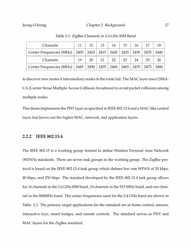
Table 2.1: ZigBee Channels in 2.4 GHz ISM Band
Channels 11 12 13 14 15 16 17 18
Center Frequencies (MHz) 2405 2410 2415 2420 2425 2430 2435 2440
Channels 19 20 21 22 23 24 25 26
Center Frequencies (MHz) 2445 2450 2455 2460 2465 2470 2475 2480
to discover new routes if intermediary nodes in the route fail. The MAC layer uses CSMA-
CA (Carrier Sense Multiple Access Collision Avoidance) to avoid packet collisions among
multiple nodes.
This thesis implements the PHY layer as specified in IEEE 802.15.4 and a MAC-like control
layer, but leaves out the higher MAC, network, and application layers.
2.2.2 IEEE 802.15.4
The IEEE 802.15 is a working group formed to define Wireless Personal Area Network
(WPAN) standards. There are seven task groups in the working group. The ZigBee pro-
tocol is based on the IEEE 802.15.4 task group which defines low rate WPAN of 20 kbps,
40 kbps, and 250 kbps. The standard developed by the IEEE 802.15.4 task group allows
for 16 channels in the 2.4 GHz ISM band, 10 channels in the 915 MHz band, and one chan-
nel in the 868MHz band. The center frequencies used for the 2.4 GHz band are shown in
Table 2.1. The primary target applications for the standard are in home control, sensors,
interactive toys, smart badges, and remote controls. The standard serves as PHY and
MAC layers for the ZigBee standard.

Jeong-O Jeong Chapter 2. Background 18
Figure 2.2: IEEE 802.15.4 Data Frame [1]
IEEE 802.15.4 Frame Structure
There are four different types of frames defined at the MAC sub-layer. They include
beacon frame, data frame, acknowledgment frame, and MAC command frame. Beacon
frames are used to synchronize the nodes in the network for slotted CSMA-CA. Data
frames are used for all transfers of data between nodes. Acknowledgment frames are
used for confirmation of successful reception of data or MAC command frames. If the
transmitter does not receive the acknowledgment frame, it will retransmit. MAC com-
mand frames are used for transmitting low-level MAC commands. The data frame shown
in Figure 2.2 was implemented in this thesis.
The MAC sub-layer frame is embedded into the PSDU (Physical Layer Service Data Unit)
of the PHY layer. The PSDU is prefixed with SHR (synchronization header) and PHR
(PHY header) to be transmitted over the air. Within SHR, Preamble Sequence is used by
the receiver to detect and synchronize to the received packets. The preamble is simply all
zero bits for all PHYs except for the ASK PHY. For the 2.4 GHz O-QPSK , the preamble is
4 octets of zeros, as shown in Table 2.2, equivalent to 8 symbols, and it is 128 us long [1].
The SFD (Start of Frame Delimiter) field indicates the start of PHR. For 2.4 GHz O-QPSK,

Jeong-O Jeong Chapter 2. Background 19
Table 2.2: Preamble Field [1]
Bits 0: 1 2 3 4 5 6 7 8 9 10 11 12 13 14 15
0 0 0 0 0 0 0 0 0 0 0 0 0 0 0 0
16 17 18 19 20 21 22 23 24 25 26 27 28 29 30 31
0 0 0 0 0 0 0 0 0 0 0 0 0 0 0 0
Table 2.3: SFD Field [1]
Bits 0: 1 2 3 4 5 6 7
1 1 1 0 0 1 0 1
the SFD field is 8 bits long as shown in Table 2.3.
The Frame Length field is a 7 bits long field indicating the total number of octets in the
PSDU. The valid frame length values are from 9 to aMaxPHYPacketSize of 127. The Frame
Length field is followed by a reserved bit.
2450 MHz PHY specifications
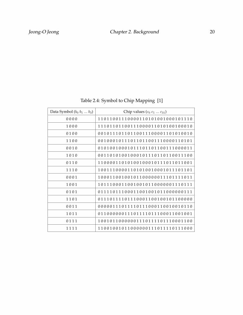
The 2450 MHz PHY specification of IEEE 802.15.4 supports data rate of up to 250kb/s.
It uses DS-SS (Direct Sequence Spread Spectrum) with O-QPSK (Offset-QPSK) for mod-
ulation. Each O-QPSK symbol is one of 16 quasi-orthogonal pseudo-random noise (PN)
sequences. Each symbol is 32-chip long and corresponds to one of 16 possible combina-
tions of four information bits. The mapping of 4-bit symbol to 32-chip sequence is shown
in Figure 2.4.
Jeong-O Jeong Chapter 2. Background 20
Table 2.4: Symbol to Chip Mapping [1]
Data Symbol (b0 b1 ... b3) Chip values (c0 c1 ... c31)
0 0 0 0 1 1 0 1 1 0 0 1 1 1 0 0 0 0 1 1 0 1 0 1 0 0 1 0 0 0 1 0 1 1 1 0
1 0 0 0 1 1 1 0 1 1 0 1 1 0 0 1 1 1 0 0 0 0 1 1 0 1 0 1 0 0 1 0 0 0 1 0
0 1 0 0 0 0 1 0 1 1 1 0 1 1 0 1 1 0 0 1 1 1 0 0 0 0 1 1 0 1 0 1 0 0 1 0
1 1 0 0 0 0 1 0 0 0 1 0 1 1 1 0 1 1 0 1 1 0 0 1 1 1 0 0 0 0 1 1 0 1 0 1
0 0 1 0 0 1 0 1 0 0 1 0 0 0 1 0 1 1 1 0 1 1 0 1 1 0 0 1 1 1 0 0 0 0 1 1
1 0 1 0 0 0 1 1 0 1 0 1 0 0 1 0 0 0 1 0 1 1 1 0 1 1 0 1 1 0 0 1 1 1 0 0
0 1 1 0 1 1 0 0 0 0 1 1 0 1 0 1 0 0 1 0 0 0 1 0 1 1 1 0 1 1 0 1 1 0 0 1
1 1 1 0 1 0 0 1 1 1 0 0 0 0 1 1 0 1 0 1 0 0 1 0 0 0 1 0 1 1 1 0 1 1 0 1
0 0 0 1 1 0 0 0 1 1 0 0 1 0 0 1 0 1 1 0 0 0 0 0 0 1 1 1 0 1 1 1 1 0 1 1
1 0 0 1 1 0 1 1 1 0 0 0 1 1 0 0 1 0 0 1 0 1 1 0 0 0 0 0 0 1 1 1 0 1 1 1
0 1 0 1 0 1 1 1 1 0 1 1 1 0 0 0 1 1 0 0 1 0 0 1 0 1 1 0 0 0 0 0 0 1 1 1
1 1 0 1 0 1 1 1 0 1 1 1 1 0 1 1 1 0 0 0 1 1 0 0 1 0 0 1 0 1 1 0 0 0 0 0
0 0 1 1 0 0 0 0 0 1 1 1 0 1 1 1 1 0 1 1 1 0 0 0 1 1 0 0 1 0 0 1 0 1 1 0
1 0 1 1 0 1 1 0 0 0 0 0 0 1 1 1 0 1 1 1 1 0 1 1 1 0 0 0 1 1 0 0 1 0 0 1
0 1 1 1 1 0 0 1 0 1 1 0 0 0 0 0 0 1 1 1 0 1 1 1 1 0 1 1 1 0 0 0 1 1 0 0
1 1 1 1 1 1 0 0 1 0 0 1 0 1 1 0 0 0 0 0 0 1 1 1 0 1 1 1 1 0 1 1 1 0 0 0
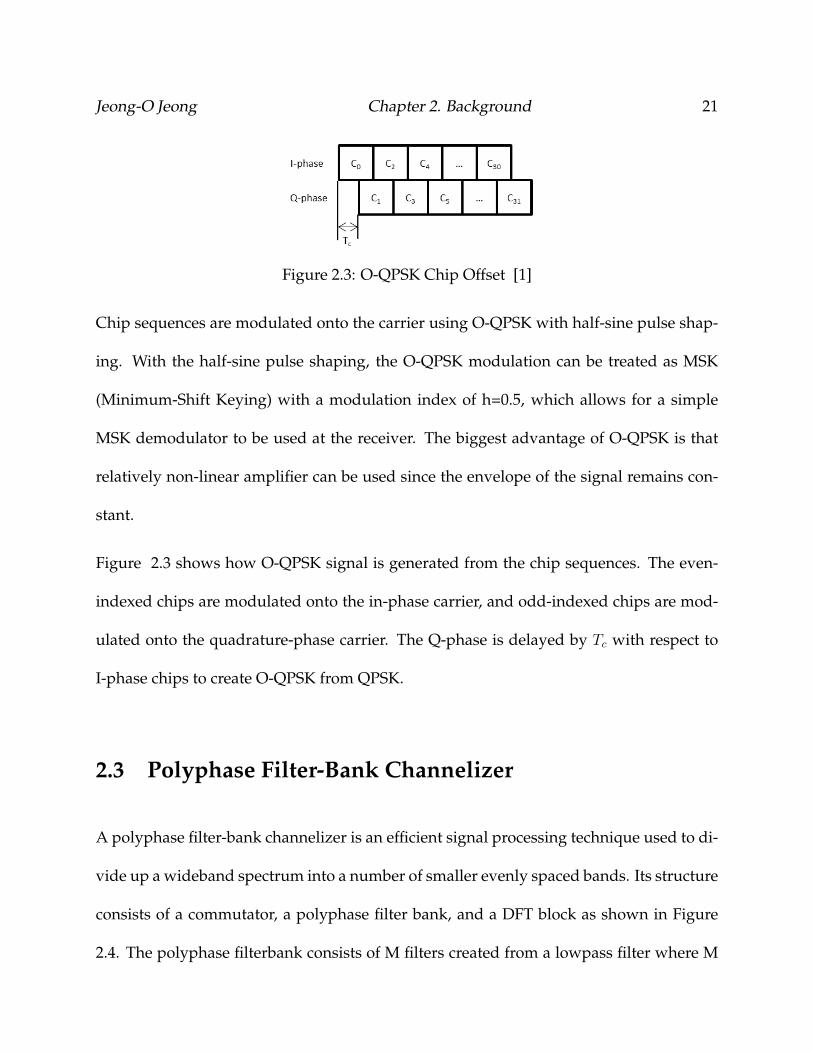
Jeong-O Jeong Chapter 2. Background 21
Figure 2.3: O-QPSK Chip Offset [1]
Chip sequences are modulated onto the carrier using O-QPSK with half-sine pulse shap-
ing. With the half-sine pulse shaping, the O-QPSK modulation can be treated as MSK
(Minimum-Shift Keying) with a modulation index of h=0.5, which allows for a simple
MSK demodulator to be used at the receiver. The biggest advantage of O-QPSK is that
relatively non-linear amplifier can be used since the envelope of the signal remains con-
stant.
Figure 2.3 shows how O-QPSK signal is generated from the chip sequences. The even-
indexed chips are modulated onto the in-phase carrier, and odd-indexed chips are mod-
ulated onto the quadrature-phase carrier. The Q-phase is delayed by Tc with respect to
I-phase chips to create O-QPSK from QPSK.
2.3 Polyphase Filter-Bank Channelizer
A polyphase filter-bank channelizer is an efficient signal processing technique used to di-
vide up a wideband spectrum into a number of smaller evenly spaced bands. Its structure
consists of a commutator, a polyphase filter bank, and a DFT block as shown in Figure
2.4. The polyphase filterbank consists of M filters created from a lowpass filter where M

Jeong-O Jeong Chapter 2. Background 22
Figure 2.4: Polyphase Channelizer
is the number of channels.
The lowpass filter used to create the polyphase bank can be written as a one-dimensional
array of coefficients as the following in the z-domain.
H(z) =N−1∑n=0
h[n]z−n (2.3)
= h[0] + h[1]z−1 + h[2]z−2 + . . .+ h[N − 1]z−(N−1)
The coefficients can be rearranged as a two-dimensional array where the number of rows
is M as shown in Equation 2.4.
H(z) = h[0] + h[M + 0]z−M + h[2M + 0]z−2M + . . . (2.4)
+ h[1]z−1 + h[M + 1]z−(M+1) + h[2M + 1]z−(2M+1) + . . .
+ h[2]z−2 + h[M + 2]z−(M+2) + h[2M + 2]z−(2M+2) + . . .
. . .
+ h[M − 1]z−(M−1) + h[2M − 1]z−(2M−1) + h[3M − 1]z−(3M−1) + . . .

Jeong-O Jeong Chapter 2. Background 23
Figure 2.5: Single Channel M-to-1 Resampler
Each row of Equation 2.4 can be grouped together so that H(z) can be re-written in the
following way.
H(z) = H0(zM) (2.5)
+ z−1H1(zM)
+ z−2H2(zM)
+ . . .
+ z−(M−1)HM−1(zM)
where H0(zM) is the terms in the first row of Equation 2.4, z−1H1(zM) is the terms in the
second row, and so on.
The M terms in Equation 2.5 correspond to the M filters in the polyphase filter bank. The
commutator act as the delay factors in front of the M terms. Given M channels, Figure
2.5 shows the resampler structure where a channel centered at kth center frequency can
Jeong-O Jeong Chapter 2. Background 24
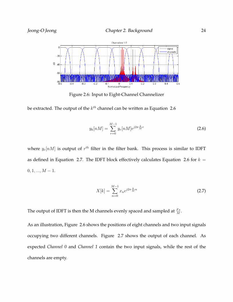
Figure 2.6: Input to Eight-Channel Channelizer
be extracted. The output of the kth channel can be written as Equation 2.6
yk[nM ] =M−1∑r=0
yr[nM ]ej2πkMr (2.6)
where yr[nM ] is output of rth filter in the filter bank. This process is similar to IDFT
as defined in Equation 2.7. The IDFT block effectively calculates Equation 2.6 for k =
0, 1, ...,M − 1.
X[k] =M−1∑n=0
xnej2π k
Mn (2.7)
The output of IDFT is then the M channels evenly spaced and sampled at FsM
.
As an illustration, Figure 2.6 shows the positions of eight channels and two input signals
occupying two different channels. Figure 2.7 shows the output of each channel. As
expected Channel 0 and Channel 1 contain the two input signals, while the rest of the
channels are empty.

Jeong-O Jeong Chapter 2. Background 25
Figure 2.7: Output of Each Channel
Table 2.5: USRP N210 Specification
FPGA Xilinx Spartan 3A-DSP3400
ADC 14-bits 100 MS/s
DAC 16-bits 400 MS/s
RF Bandwidth50 MHz of instantaneous RF bandwidth in 8-bit mode
25 MHz of instantaneous RF bandwidth in 16-bit mode
Connectivity Gigabit Ethernet Interface
2.4 USRP N210
The USRP (Universal Software Radio Peripheral) is a family of software radio platforms
developed by Ettus Research LLC. Table 2.5 shows the summary of specifications of
USRP N210 [22].
The USRP2, the predecessor of the USRP N210, has almost identical features as the USRP
N210, except that it has a smaller Xilinx Spartan 3-2000 FPGA. Table 2.6 compares the
FPGAs on USRP N210 and USRP2.
Jeong-O Jeong Chapter 2. Background 26
Table 2.6: FPGAs of USRP N210 (3A3400) and USRP2 (3S2000)
FPGASystem
Gates
Equi-
valent
Logic
Cells
Total
Slices
Distri-
buted
RAM
Bits
Block
RAM
Bits
DSP48As
Dedi-
cated
Multi-
pliers
DCMs
Max-
imum
USER
I/O
3A3400 3400K 53,712 23,872 373K 2258K 126 N/A 8 469
3S2000 2000K 46,080 20,480 320K 720K N/A 40 4 565
2.4.1 Signal Processing in FPGA of USRP N210
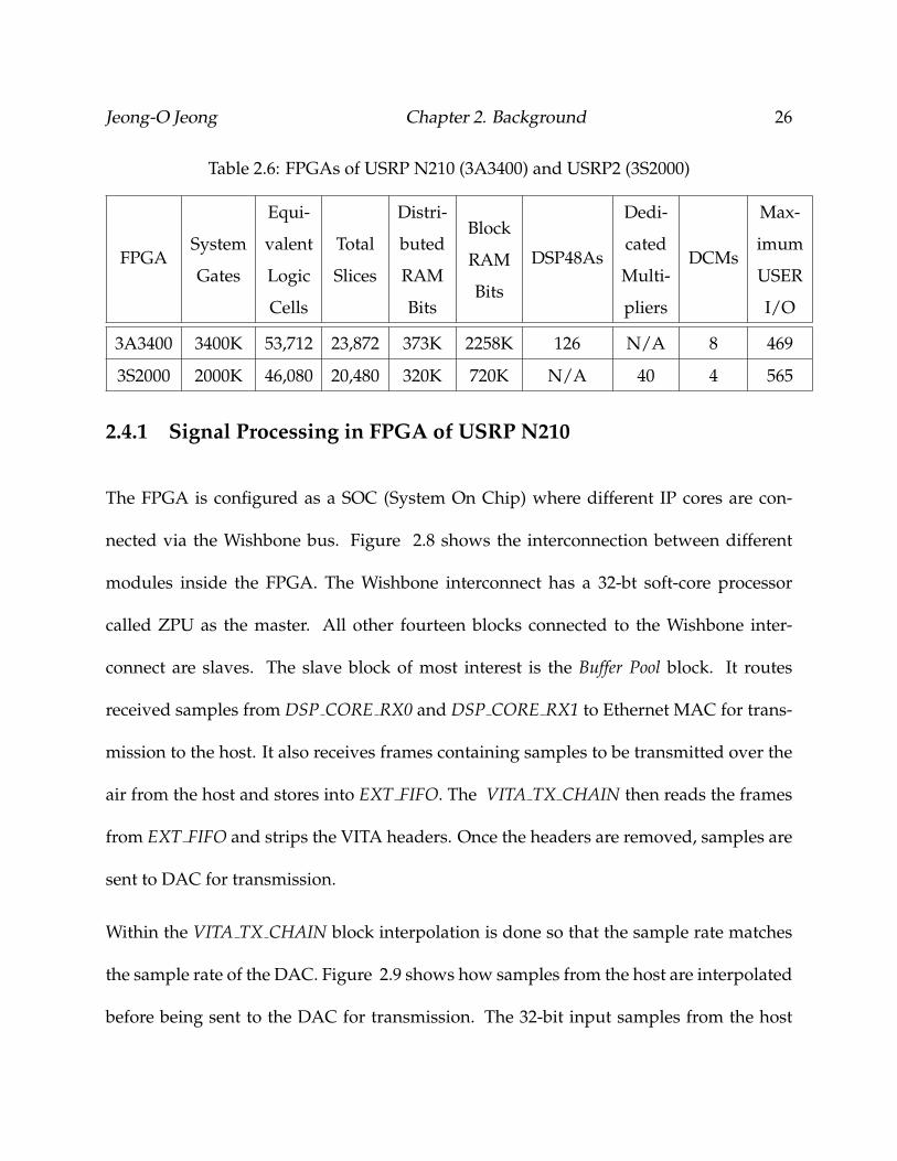
The FPGA is configured as a SOC (System On Chip) where different IP cores are con-
nected via the Wishbone bus. Figure 2.8 shows the interconnection between different
modules inside the FPGA. The Wishbone interconnect has a 32-bt soft-core processor
called ZPU as the master. All other fourteen blocks connected to the Wishbone inter-
connect are slaves. The slave block of most interest is the Buffer Pool block. It routes
received samples from DSP CORE RX0 and DSP CORE RX1 to Ethernet MAC for trans-
mission to the host. It also receives frames containing samples to be transmitted over the
air from the host and stores into EXT FIFO. The VITA TX CHAIN then reads the frames
from EXT FIFO and strips the VITA headers. Once the headers are removed, samples are
sent to DAC for transmission.
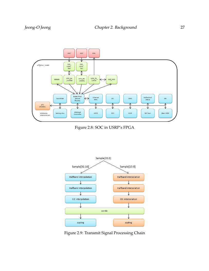
Within the VITA TX CHAIN block interpolation is done so that the sample rate matches
the sample rate of the DAC. Figure 2.9 shows how samples from the host are interpolated
before being sent to the DAC for transmission. The 32-bit input samples from the host
Jeong-O Jeong Chapter 2. Background 27
Figure 2.8: SOC in USRP’s FPGA
Figure 2.9: Transmit Signal Processing Chain
Jeong-O Jeong Chapter 2. Background 28
Figure 2.10: Time-Domain Plot of First Half-Band Filter
are divided into 16-bit in-phase samples and 16-bit quadrature-phase samples. The first
half-band filter interpolates the samples by a factor of two if the filter is enabled. The
second half-band filter interpolates the signal again by another factor of two if enabled.
The CIC interpolator can interpolate the signal up to a factor of 128. Thus, the maximum
interpolation rate within the FPGA is 512. The 24-stage CORDIC block rotates the signal
to give frequency offset before being up-converted by the daughterboard.
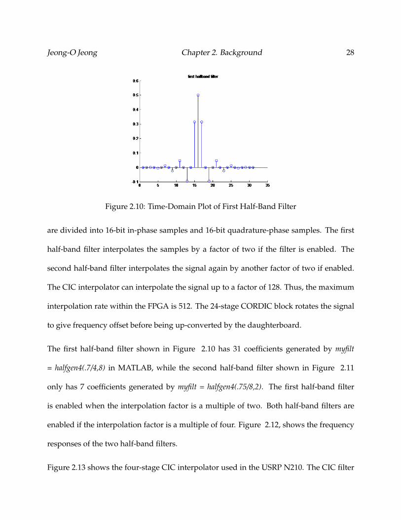
The first half-band filter shown in Figure 2.10 has 31 coefficients generated by myfilt
= halfgen4(.7/4,8) in MATLAB, while the second half-band filter shown in Figure 2.11
only has 7 coefficients generated by myfilt = halfgen4(.75/8,2). The first half-band filter
is enabled when the interpolation factor is a multiple of two. Both half-band filters are
enabled if the interpolation factor is a multiple of four. Figure 2.12, shows the frequency
responses of the two half-band filters.
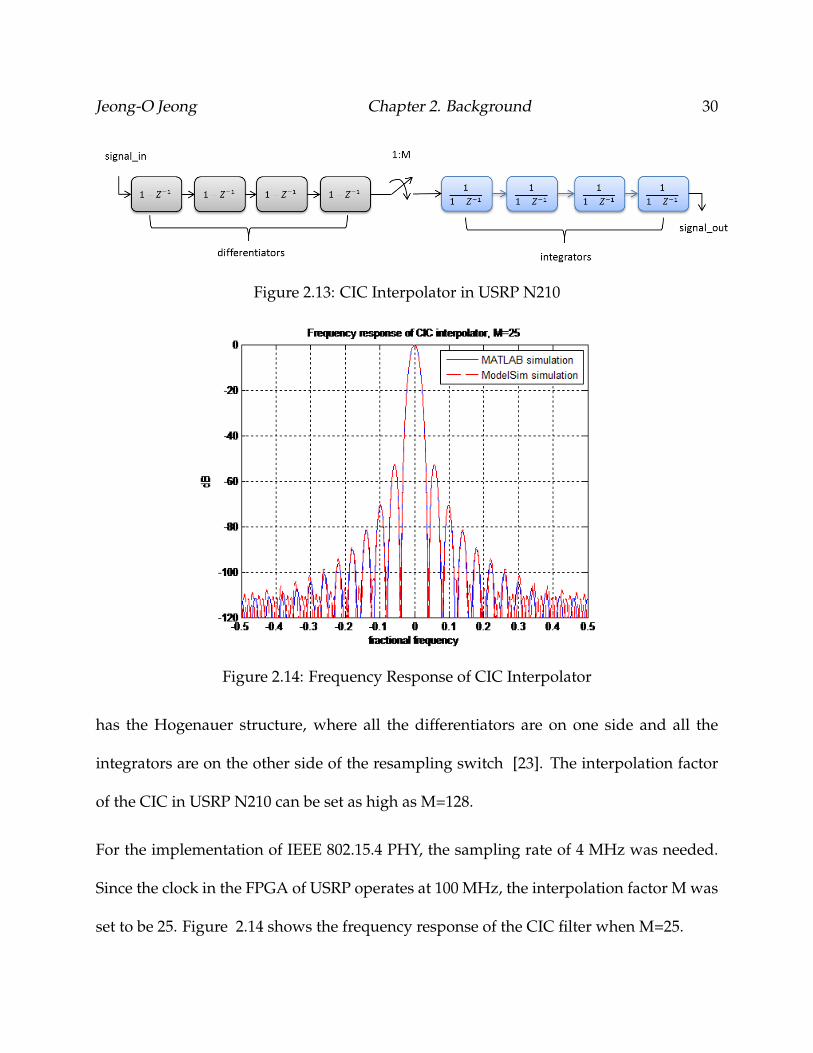
Figure 2.13 shows the four-stage CIC interpolator used in the USRP N210. The CIC filter

Jeong-O Jeong Chapter 2. Background 29
Figure 2.11: Time-Domain Plot of Second Half-Band Filter
Figure 2.12: Frequency Response of Two Halfband Filters
Jeong-O Jeong Chapter 2. Background 30
Figure 2.13: CIC Interpolator in USRP N210
Figure 2.14: Frequency Response of CIC Interpolator
has the Hogenauer structure, where all the differentiators are on one side and all the
integrators are on the other side of the resampling switch [23]. The interpolation factor
of the CIC in USRP N210 can be set as high as M=128.
For the implementation of IEEE 802.15.4 PHY, the sampling rate of 4 MHz was needed.
Since the clock in the FPGA of USRP operates at 100 MHz, the interpolation factor M was
set to be 25. Figure 2.14 shows the frequency response of the CIC filter when M=25.
Jeong-O Jeong Chapter 2. Background 31
Figure 2.15: Receiver Signal Processing Chain
In the receiver chain, the reverse of the transmitter chain happens. The DSP CORE RX
core in the SOC receives the samples from the ADC. Inside the DSP CORE RX core, the
CORDIC block performs digital down-conversion (DDC). After the DDC is performed,
the samples are decimated with the two half-band decimators and the CIC filter. After
decimation, the samples are sent to the VRT (VITA Radio Transport) core for packeti-
zation. The packets are then sent to the Ethernet MAC to be transported to the host
computer.

Chapter 3
Methodology and Implementation
For this thesis, two major signal processing blocks, IEEE 802.15.4 PHY and a polyphase
filter-bank channelizer, have been implemented in Spartan 3A-DSP FPGA of USRP N210
and Virtex 5 FPGA, respectively. This section illustrates the steps taken to simulate and
implement the blocks.
3.1 IEEE 802.15.4 PHY on FPGA
There are two paths explored in implementing the IEEE 802.15.4 PHY, as shown in Figure
3.1. The first path involves Simulink modeling, while the second one does not. In the first
path, the floating-point simulation is performed in MATLAB which is then converted to
a Simulink model. At this stage, the Simulink model is still in floating-point. In order to
32
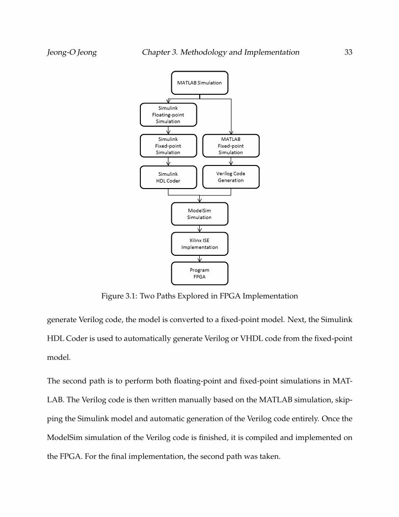
Jeong-O Jeong Chapter 3. Methodology and Implementation 33
Figure 3.1: Two Paths Explored in FPGA Implementation
generate Verilog code, the model is converted to a fixed-point model. Next, the Simulink
HDL Coder is used to automatically generate Verilog or VHDL code from the fixed-point
model.
The second path is to perform both floating-point and fixed-point simulations in MAT-
LAB. The Verilog code is then written manually based on the MATLAB simulation, skip-
ping the Simulink model and automatic generation of the Verilog code entirely. Once the
ModelSim simulation of the Verilog code is finished, it is compiled and implemented on
the FPGA. For the final implementation, the second path was taken.
Jeong-O Jeong Chapter 3. Methodology and Implementation 34
Figure 3.2: Overall Setup of IEEE 802.15.4 PHY on FPGA
3.1.1 Configuration
Figure 3.2 shows the overall setup of the system. In normal receive mode, USRP N210
sends the data samples to GNU Radio after down-conversion and some filtering. How-
ever, when the IEEE 802.15.4 PHY receiver is enabled, the receiver resides between the
DDC and Ethernet interface and intercepts the samples and processes them before send-
ing the result to the Ethernet interface. Likewise, in transmit mode, USRP N210 nor-
mally sends samples from GNU Radio to DUC for transmission. However, when the
IEEE 802.15.4 PHY transmitter is enabled, it intercepts the samples from GNU Radio and
modulates the samples before sending them to DUC.

Jeong-O Jeong Chapter 3. Methodology and Implementation 35
Figure 3.3: Overall Transmitter Chain
Figure 3.4: Simulation of O-QPSK at Baseband
3.1.2 Transmitter
MATLAB Simulation
The first step in implementation of the IEEE 802.15.4 transmitter is to simulate the signal
processing chain, shown in Figure 3.3, in MATLAB. IEEE 802.15.4 frames are generated
using the PPDU (PHY Protocol Data Unit) generator function. The PPDU bits are then
grouped as quad-bits and mapped to symbols. The symbols are spread to give overall
spreading factor of eight. The final output of the transmitter chain is the baseband I and
Q as shown in Figure 3.4. The baseband signal is an O-QPSK signal where the quadrature
Jeong-O Jeong Chapter 3. Methodology and Implementation 36
Figure 3.5: Transmitter Chain
component is delayed by half the symbol period.
RTL Implementation/Simulation
After simulation in MATLAB and/or Simulink, the algorithm must be converted to Ver-
ilog. The signal chain is modularized so that blocks can be mapped onto the existing GNU
Radio implementation of ZigBee Radio [12]. Some of the blocks such as gr.packed to unpacked
and gr.chunks to symbols are based on the basic blocks provided by the GNU Radio library
written in C++. The blocks developed for the thesis can be used in GReasy as basic build-
ing blocks for other complex signal processing applications.
Figure 3.5 shows the RTL blocks in the transmitter signal processing chain. The zb symbols
to chips block breaks the bytes from the incoming payload into two separate four-bit sym-
bols, each of which are then mapped to one of the sixteen chip sequences as was shown
in Figure 2.4.
For example, if the current byte is 0x14, it is broken into two four-bit symbols, 0x1 and
0x4. The first symbol 0x1 is mapped to the chip 398643741010, and the second symbol 0x4
is mapped to the chip 137880211510. The clock rate increases from 250kbps to 2Mchips/s
Jeong-O Jeong Chapter 3. Methodology and Implementation 37
at the output.
The gr.packed to unpacked block breaks the 32-chip long chip sequences into 16 two-chip
chunks. For example, the chip 137880211510 (010100100010111011011001110000112), is bro-
ken into chunks of 01, 01, 00, 10, 00, 10, 11, 10, 11, 01, 10, 01, 11, 00, 00, and 11. The clock
rate is decreased by a factor of two from 2Mchips/s to 1Mchunks/s, or 1 M QPSK sym-
bols/s at the output.
The gr.chunks to symbols block maps each chunk to a point on the QPSK constellation.
Using gray coding, the chunk 00 is mapped to -1-j, 01 to -1+j, 10 to 1-j, and 11 to 1+j. The
clock rate stays the same at the output.
The zb.half sine pulse block performs half-sine pulse-shaping of the QPSK symbols. The
pulse-shaping is done by a simple mapping of the constellations to a positive half-sine
pulse or a negative half-sine pulse depending on the data. For example, when the in-
phase or the quadrature-phase is a ’1’, it is mapped to the positive pulse. If it is a ’-1’, it is
mapped to a negative half-sine pulse. The pulses used are up-sampled by a factor of four.
Therefore, the clock rate is increased by a factor of four at the output to be 4 M samples/s.
Finally, in order to generate O-QPSK signal from the QPSK signal, the quadrature com-
ponent is delayed by two samples by the zb.delay cc block.
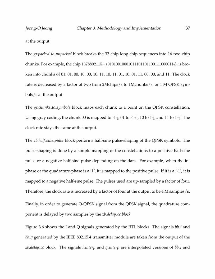
Figure 3.6 shows the I and Q signals generated by the RTL blocks. The signals bb i and
bb q generated by the IEEE 802.15.4 transmitter module are taken from the output of the
zb.delay cc block. The signals i interp and q interp are interpolated versions of bb i and
Jeong-O Jeong Chapter 3. Methodology and Implementation 38
Figure 3.6: ModelSim simulation of transmitted signal
bb q. The interpolation is done inside the USRP N210’s FPGA CIC interpolator blocks.
The interpolated signal is up-converted and sent to the DAC for transmission over the
air.
FPGA Implementation
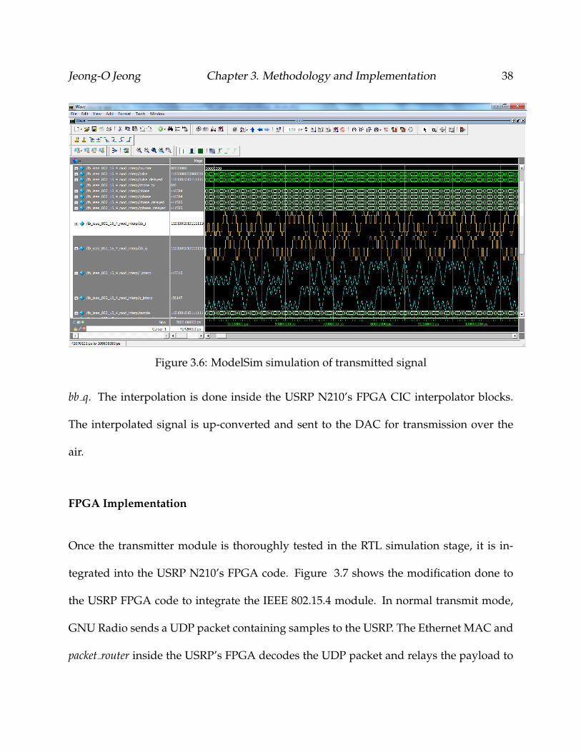
Once the transmitter module is thoroughly tested in the RTL simulation stage, it is in-
tegrated into the USRP N210’s FPGA code. Figure 3.7 shows the modification done to
the USRP FPGA code to integrate the IEEE 802.15.4 module. In normal transmit mode,
GNU Radio sends a UDP packet containing samples to the USRP. The Ethernet MAC and
packet router inside the USRP’s FPGA decodes the UDP packet and relays the payload to
Jeong-O Jeong Chapter 3. Methodology and Implementation 39
Figure 3.7: Transmitter module inside USRP’s FPGA
vita tx chain. The VRT headers are then removed by deframer and vita tx control, and the
extracted samples are sent to dsp tx core where they are interpolated and sent to the DAC
for transmission. The FPGA code was modified so that the samples from vita tx control are
sent to the IEEE 802.15.4 transmitter instead of dsp tx core. The output of the IEEE 802.15.4
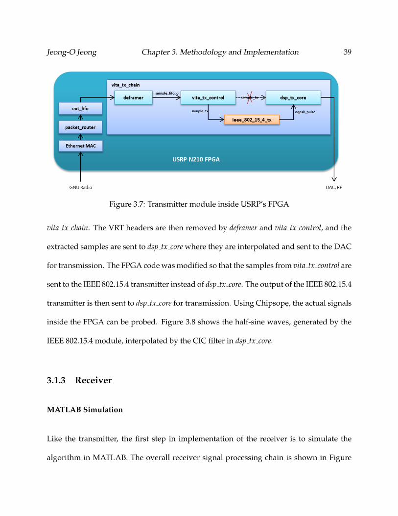
transmitter is then sent to dsp tx core for transmission. Using Chipsope, the actual signals
inside the FPGA can be probed. Figure 3.8 shows the half-sine waves, generated by the
IEEE 802.15.4 module, interpolated by the CIC filter in dsp tx core.
3.1.3 Receiver
MATLAB Simulation
Like the transmitter, the first step in implementation of the receiver is to simulate the
algorithm in MATLAB. The overall receiver signal processing chain is shown in Figure
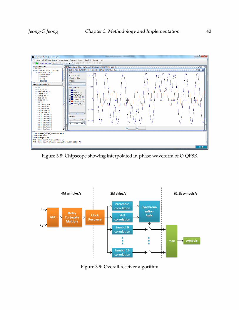
Jeong-O Jeong Chapter 3. Methodology and Implementation 40
Figure 3.8: Chipscope showing interpolated in-phase waveform of O-QPSK
Figure 3.9: Overall receiver algorithm

Jeong-O Jeong Chapter 3. Methodology and Implementation 41
Figure 3.10: AGC Structure
3.9.
Automatic Gain Control
The automatic gain control (AGC) block is needed at the input of the receiver to utilize as
much dynamic range as possible. When the magnitude of the input samples is small, the
inverse tangent function block in FPGA implementation is not able to produce accurate
outputs as shown in the later section. The structure of the AGC block based on the GNU
Radio implementation AGC2 is shown in Figure 3.10.
Demodulation of O-QPSK as MSK
The O-QPSK modulated waveform can be demodulated as MSK when half-sine pulse
shaping is used, as is the case with IEEE 802.15.4 [24]. An MSK waveform can be de-
modulated using the delay-conjugate-multiply shown in Figure 3.11, since the output
of the delay-conjugate-multiply block is the phase change between two consecutive sam-
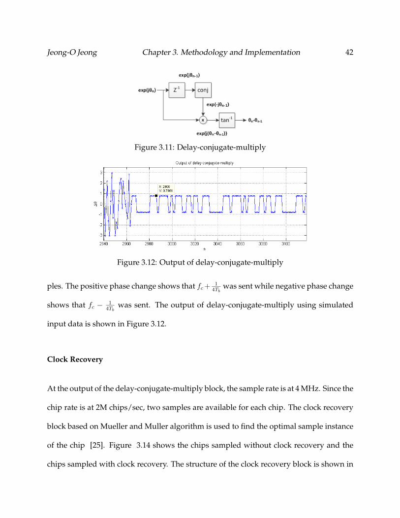
Jeong-O Jeong Chapter 3. Methodology and Implementation 42
Figure 3.11: Delay-conjugate-multiply
Figure 3.12: Output of delay-conjugate-multiply
ples. The positive phase change shows that fc+ 14Tb
was sent while negative phase change
shows that fc − 14Tb
was sent. The output of delay-conjugate-multiply using simulated
input data is shown in Figure 3.12.
Clock Recovery
At the output of the delay-conjugate-multiply block, the sample rate is at 4 MHz. Since the
chip rate is at 2M chips/sec, two samples are available for each chip. The clock recovery
block based on Mueller and Muller algorithm is used to find the optimal sample instance
of the chip [25]. Figure 3.14 shows the chips sampled without clock recovery and the
chips sampled with clock recovery. The structure of the clock recovery block is shown in
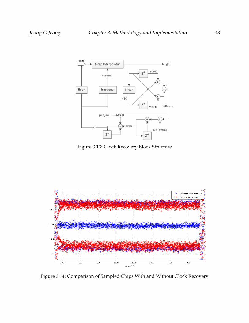
Jeong-O Jeong Chapter 3. Methodology and Implementation 43
Figure 3.13: Clock Recovery Block Structure
Figure 3.14: Comparison of Sampled Chips With and Without Clock Recovery

Jeong-O Jeong Chapter 3. Methodology and Implementation 44
Figure 3.15: Preamble and SFD correlations
Figure 3.13.
Preamble and SFD correlation thresholds
Figure 3.15 shows the preamble and SFD correlations for four consecutive PPDU frames.
Once the preamble and SFD correlations are found, they have to be compared to some
thresholds to determine if an IEEE 802.15.4 packet was actually present or not. If the
correlation values, λpreamble and λSFD, are greater than some thresholds τpreamble and τSFD,
then it is determined that a valid packet is present and the incoming samples should be
demodulated. If the correlation values are lower than the thresholds, it is determined
that there is no valid packet present. A simple binary hypothesis testing can be used to
Jeong-O Jeong Chapter 3. Methodology and Implementation 45
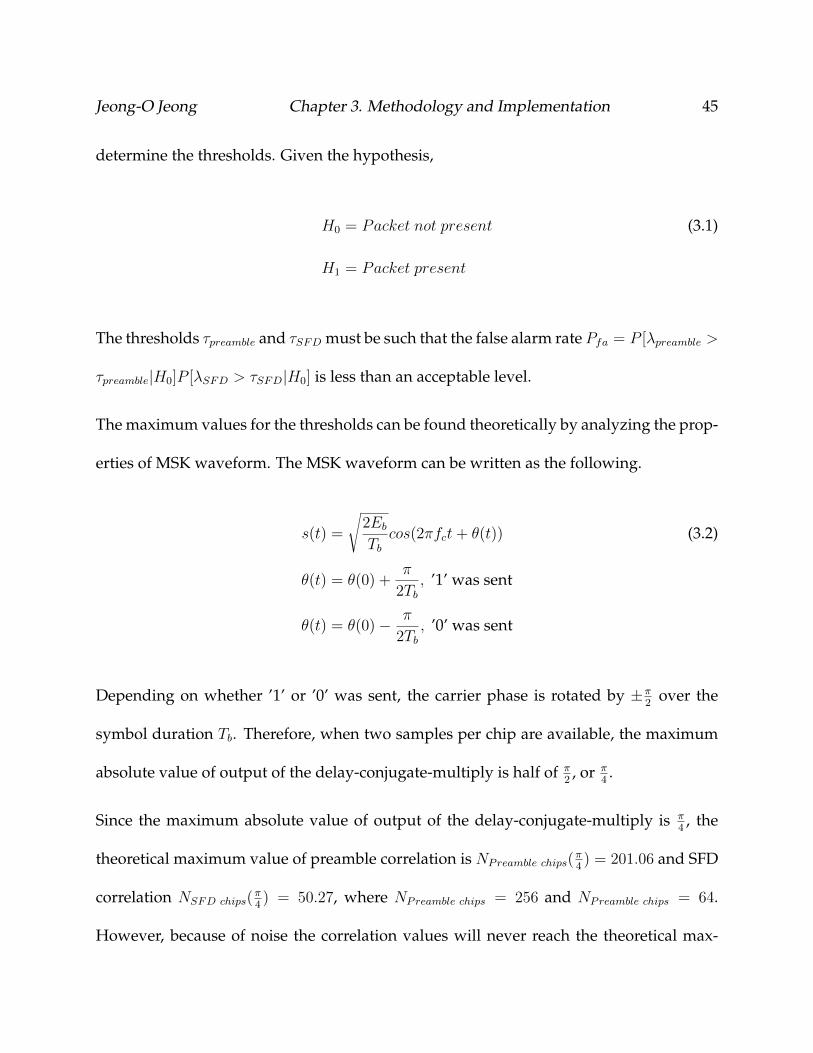
determine the thresholds. Given the hypothesis,
H0 = Packet not present (3.1)
H1 = Packet present
The thresholds τpreamble and τSFD must be such that the false alarm rate Pfa = P [λpreamble >
τpreamble|H0]P [λSFD > τSFD|H0] is less than an acceptable level.
The maximum values for the thresholds can be found theoretically by analyzing the prop-
erties of MSK waveform. The MSK waveform can be written as the following.
s(t) =
√2EbTb
cos(2πfct+ θ(t)) (3.2)
θ(t) = θ(0) +π
2Tb, ’1’ was sent
θ(t) = θ(0)− π
2Tb, ’0’ was sent
Depending on whether ’1’ or ’0’ was sent, the carrier phase is rotated by ±π2
over the
symbol duration Tb. Therefore, when two samples per chip are available, the maximum
absolute value of output of the delay-conjugate-multiply is half of π2, or π
4.
Since the maximum absolute value of output of the delay-conjugate-multiply is π4, the
theoretical maximum value of preamble correlation is NPreamble chips(π4) = 201.06 and SFD
correlation NSFD chips(π4) = 50.27, where NPreamble chips = 256 and NPreamble chips = 64.
However, because of noise the correlation values will never reach the theoretical max-

Jeong-O Jeong Chapter 3. Methodology and Implementation 46
imum values. Therefore, the thresholds of preamble and SFD correlations have to be
somewhat lower for the packets to be detected. The actual threshold values used for
implementation are determined experimentally as shown in later sections.
Symbol Correlations
Once the SFD is found, the receiver must decide which symbol was sent by the trans-
mitter. The decision of which symbol was sent is made by picking the symbol that gives
the highest correlation value. In the GNU Radio implementation, the correlation values
are found by first slicing the chips at the output of the delay-conjugate-multiply mod-
ule, which is similar to hard-decision decoding. In this implementation, the chips are not
sliced, but instead the soft-decision values at the output of the delay-conjugate-multiply
block is input to the correlators. As shown in Figures 3.16 and 3.17, the performance
of the receiver is better with soft decision decoding. The disadvantage of soft-decision
decoding is that it takes more processing power. In the hard-decision decoding, the cor-
relation value can be obtained by simply performing an XOR operation of the input chips
and the reference chips and then counting the number of bits that are ’0’. Whereas in soft-
decision decoding, 32-tap FIR filtering must be done for all 16 symbols. However, soft-
decision decoding gives better performance at low SNR. This is in line with the result that
Viterbi decoders give better results with soft-decision decoding in error-correcting codes
[26].

Jeong-O Jeong Chapter 3. Methodology and Implementation 47
Figure 3.16: BER Simulation of Soft vs. Hard Correlations
Figure 3.17: Packet Detection Rate Simulation of Soft vs. Hard Correlations

Jeong-O Jeong Chapter 3. Methodology and Implementation 48
Figure 3.18: Output of delay-conjugate-multiply with frequency offset of 20 KHz
Frequency Offset Estimation
Frequency offset occurs when the local oscillators at the receiver and the transmitter are
not completely in sync. This results in a slight frequency shift when the RF signal is
converted to baseband. For the O-QPSK case, when the baseband signal is demodulated
using the delay-conjugate-multiply method, it results in a slight DC offset as shown in
Figure 3.18.
The IEEE 802.15.4 standard uses a similar preamble structure as the IEEE 802.11a stan-
dard. The IEEE 802.11a standard has a preamble composed of ten short preambles repeat-
ing every 0.8us. Similarly, EEE 802.15.4 has a preamble structure which consists of eight
repeating sequence of chips every 16us. Thus, the frequency offset of the IEEE 802.15.4
packets can be estimated in a similar way as is done for the IEEE 802.11a packets [27].
The frequency offset of the received signal can be estimated using the received preamble
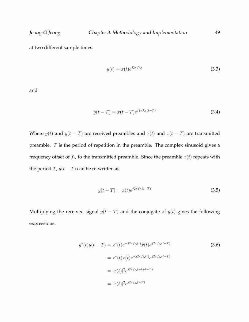
Jeong-O Jeong Chapter 3. Methodology and Implementation 49
at two different sample times.
y(t) = x(t)ej2πf∆t (3.3)
and
y(t− T ) = x(t− T )ej2πf∆(t−T ) (3.4)
Where y(t) and y(t − T ) are received preambles and x(t) and x(t − T ) are transmitted
preamble. T is the period of repetition in the preamble. The complex sinusoid gives a
frequency offset of f∆ to the transmitted preamble. Since the preamble x(t) repeats with
the period T , y(t− T ) can be re-written as
y(t− T ) = x(t)ej2πf∆(t−T ) (3.5)
Multiplying the received signal y(t − T ) and the conjugate of y(t) gives the following
expressions.
y∗(t)y(t− T ) = x∗(t)e−j2πf∆(t)x(t)ej2πf∆(t−T ) (3.6)
= x∗(t)x(t)e−j2πf∆(t)ej2πf∆(t−T )
= |x(t)|2ej2πf∆(−t+t−T )
= |x(t)|2ej2πf∆(−T )

Jeong-O Jeong Chapter 3. Methodology and Implementation 50
Taking the angle of the expression in 3.6 gives the following result.
6 y∗(t)y(t− T ) = 2πf∆(−T ) (3.7)
Dividing by an appropriate factor reveals the frequency offset of the received signal.
f∆ =2πf∆(−T )
2π(−T )(3.8)
Since the range of valid values for the result of the angle function is (−π, π], the minimum
and maximum frequency offset that can be estimated are the following.
f∆min =−π
2π(T )= −31.25kHz (3.9)
f∆max =π
2π(T )= 31.25kHz
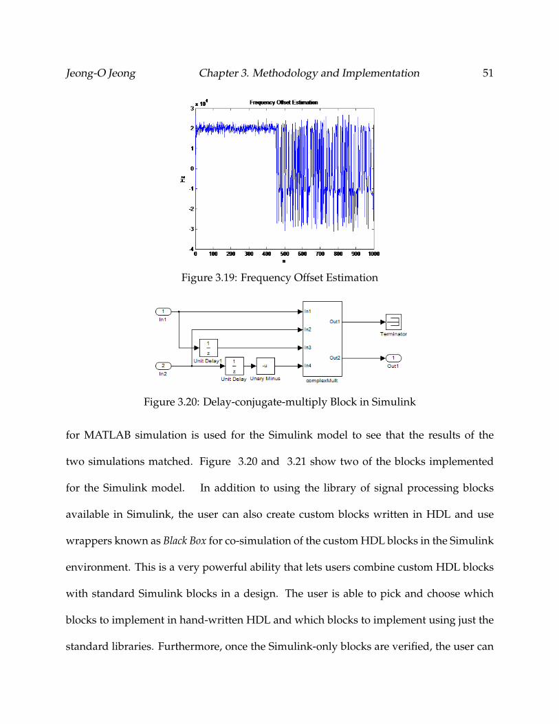
Figure 3.19 shows the output of the frequency offset estimation. During the preamble,
the simulated frequency offset of f∆ = 20 kHz is correctly estimated. However, as seen
in Figure 3.18 the delay-conjugate-multiply demodulation scheme is very robust to the
effects of frequency offset. Therefore, no frequency offset correction is needed.
Simulink Simulation
Once the signal processing chain is verified with MATLAB simulations, it is broken down
into individual blocks to be implemented in Simulink. The same input test data used
Jeong-O Jeong Chapter 3. Methodology and Implementation 51
Figure 3.19: Frequency Offset Estimation
Figure 3.20: Delay-conjugate-multiply Block in Simulink
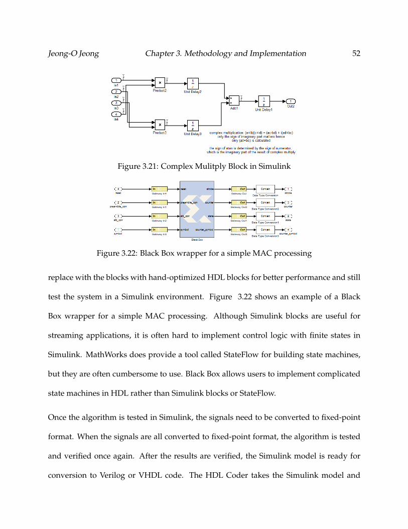
for MATLAB simulation is used for the Simulink model to see that the results of the
two simulations matched. Figure 3.20 and 3.21 show two of the blocks implemented
for the Simulink model. In addition to using the library of signal processing blocks
available in Simulink, the user can also create custom blocks written in HDL and use
wrappers known as Black Box for co-simulation of the custom HDL blocks in the Simulink
environment. This is a very powerful ability that lets users combine custom HDL blocks
with standard Simulink blocks in a design. The user is able to pick and choose which
blocks to implement in hand-written HDL and which blocks to implement using just the
standard libraries. Furthermore, once the Simulink-only blocks are verified, the user can
Jeong-O Jeong Chapter 3. Methodology and Implementation 52
Figure 3.21: Complex Mulitply Block in Simulink
Figure 3.22: Black Box wrapper for a simple MAC processing
replace with the blocks with hand-optimized HDL blocks for better performance and still
test the system in a Simulink environment. Figure 3.22 shows an example of a Black
Box wrapper for a simple MAC processing. Although Simulink blocks are useful for
streaming applications, it is often hard to implement control logic with finite states in
Simulink. MathWorks does provide a tool called StateFlow for building state machines,
but they are often cumbersome to use. Black Box allows users to implement complicated
state machines in HDL rather than Simulink blocks or StateFlow.
Once the algorithm is tested in Simulink, the signals need to be converted to fixed-point
format. When the signals are all converted to fixed-point format, the algorithm is tested
and verified once again. After the results are verified, the Simulink model is ready for
conversion to Verilog or VHDL code. The HDL Coder takes the Simulink model and
Jeong-O Jeong Chapter 3. Methodology and Implementation 53
Figure 3.23: Output of CORDIC atan without AGC
converts the blocks into ”bit-true and cycle-accurate” Verilog or VHDL code [28]. The
Black Box implementations that are already written in HDL are used as they are written.
RTL Implementation
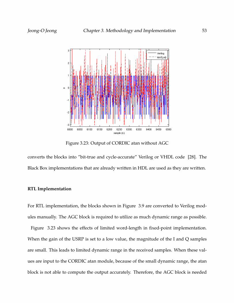
For RTL implementation, the blocks shown in Figure 3.9 are converted to Verilog mod-
ules manually. The AGC block is required to utilize as much dynamic range as possible.
Figure 3.23 shows the effects of limited word-length in fixed-point implementation.
When the gain of the USRP is set to a low value, the magnitude of the I and Q samples
are small. This leads to limited dynamic range in the received samples. When these val-
ues are input to the CORDIC atan module, because of the small dynamic range, the atan
block is not able to compute the output accurately. Therefore, the AGC block is needed

Jeong-O Jeong Chapter 3. Methodology and Implementation 54
Figure 3.24: Output of CORDIC atan with AGC
at the front of the receiver to maximize the dynamic range of the input samples. Figure
3.24 shows that the output of the atan block matches the ideal MATLAB reference when
the AGC block is introduced.
The correlations are performed using the Xilinx FIR cores. For the preamble and SFD
correlations, a 256-tap FIR filter and a 64-tap FIR filter are generated using Xilinx CORE
Generator. For the symbol correlations, 16 32-tap FIR filters are generated for each of the
16 chip sequences. The inputs to each filter are 16-bit signed soft-decision values. The
input clock period for the filters are set to 50 so that the multipliers in the DSP48 slices
could be used more efficiently by time-multiplexing. In contrast to the GNU Radio imple-
mentation, the FPGA implementation can calculate 16 correlation values simultaneously
with soft-decision values because it supports parallelism. However, the GNU Radio im-
Jeong-O Jeong Chapter 3. Methodology and Implementation 55
Figure 3.25: ModelSim Simulation Showing Preamble and SFD Corrleations
Figure 3.26: CRC-16
plementation must rely on a for-loop to iterate through the 16 correlation computations
with hard-decision chips. If the processor is not fast enough to execute the for-loop, an
overflow may occur.
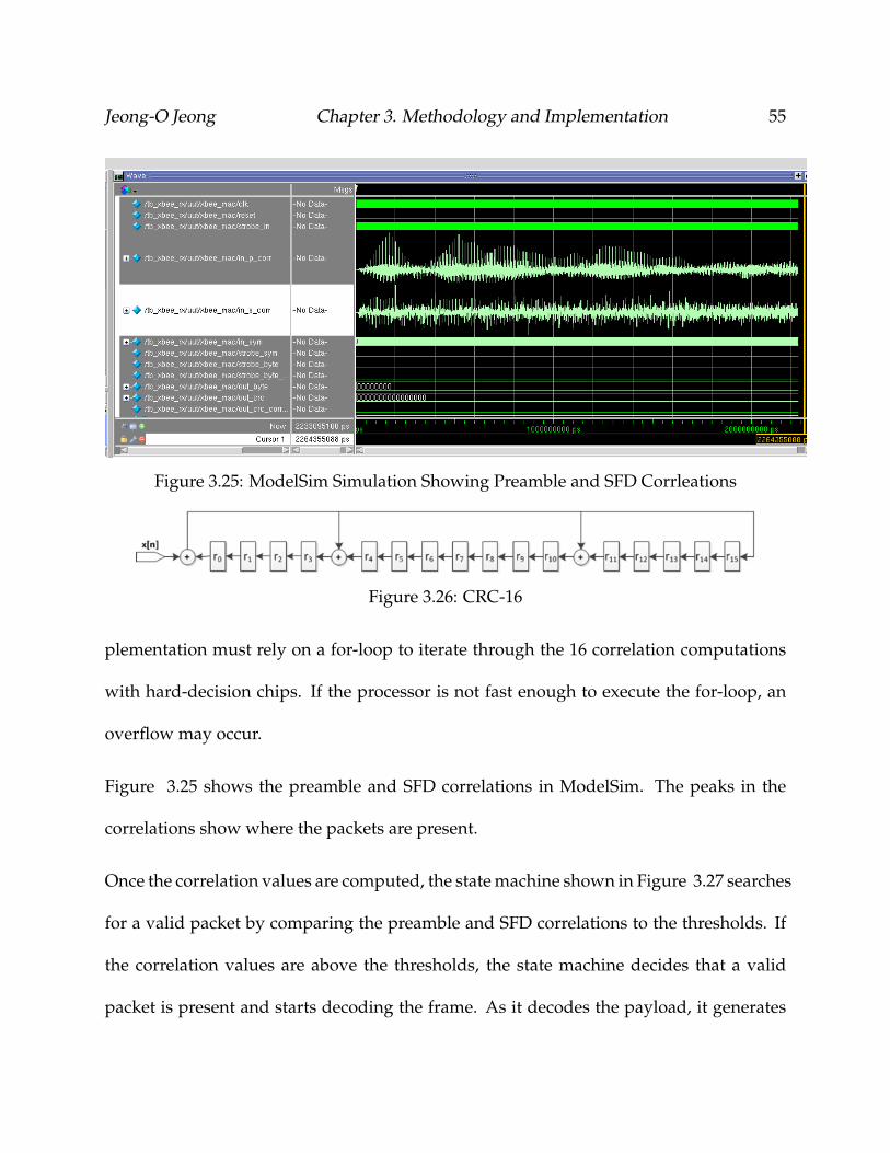
Figure 3.25 shows the preamble and SFD correlations in ModelSim. The peaks in the
correlations show where the packets are present.
Once the correlation values are computed, the state machine shown in Figure 3.27 searches
for a valid packet by comparing the preamble and SFD correlations to the thresholds. If
the correlation values are above the thresholds, the state machine decides that a valid
packet is present and starts decoding the frame. As it decodes the payload, it generates
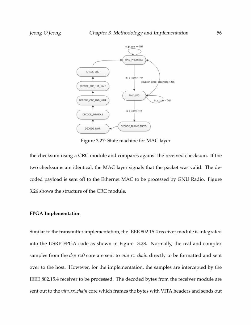
Jeong-O Jeong Chapter 3. Methodology and Implementation 56
Figure 3.27: State machine for MAC layer
the checksum using a CRC module and compares against the received checksum. If the
two checksums are identical, the MAC layer signals that the packet was valid. The de-
coded payload is sent off to the Ethernet MAC to be processed by GNU Radio. Figure
3.26 shows the structure of the CRC module.
FPGA Implementation
Similar to the transmitter implementation, the IEEE 802.15.4 receiver module is integrated
into the USRP FPGA code as shown in Figure 3.28. Normally, the real and complex
samples from the dsp rx0 core are sent to vita rx chain directly to be formatted and sent
over to the host. However, for the implementation, the samples are intercepted by the
IEEE 802.15.4 receiver to be processed. The decoded bytes from the receiver module are
sent out to the vita rx chain core which frames the bytes with VITA headers and sends out
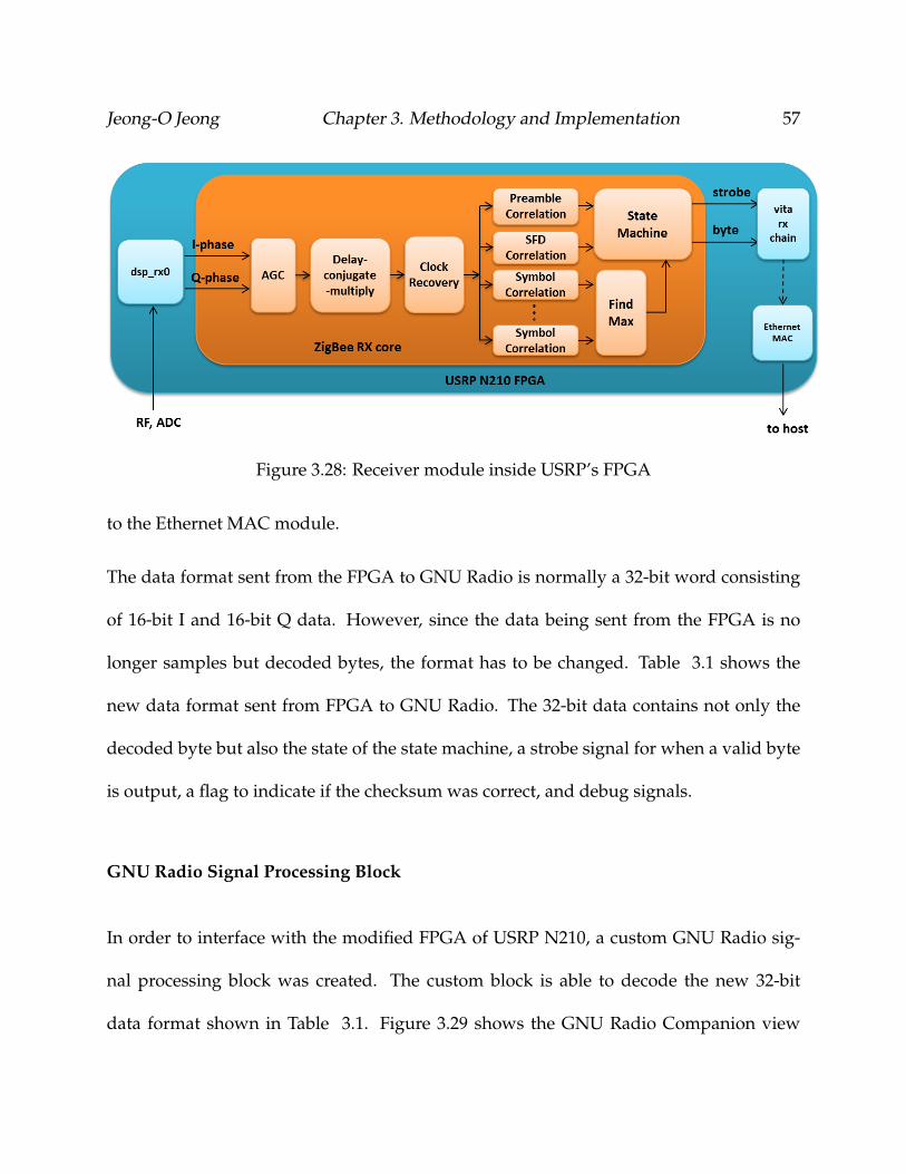
Jeong-O Jeong Chapter 3. Methodology and Implementation 57
Figure 3.28: Receiver module inside USRP’s FPGA
to the Ethernet MAC module.
The data format sent from the FPGA to GNU Radio is normally a 32-bit word consisting
of 16-bit I and 16-bit Q data. However, since the data being sent from the FPGA is no
longer samples but decoded bytes, the format has to be changed. Table 3.1 shows the
new data format sent from FPGA to GNU Radio. The 32-bit data contains not only the
decoded byte but also the state of the state machine, a strobe signal for when a valid byte
is output, a flag to indicate if the checksum was correct, and debug signals.
GNU Radio Signal Processing Block
In order to interface with the modified FPGA of USRP N210, a custom GNU Radio sig-
nal processing block was created. The custom block is able to decode the new 32-bit
data format shown in Table 3.1. Figure 3.29 shows the GNU Radio Companion view
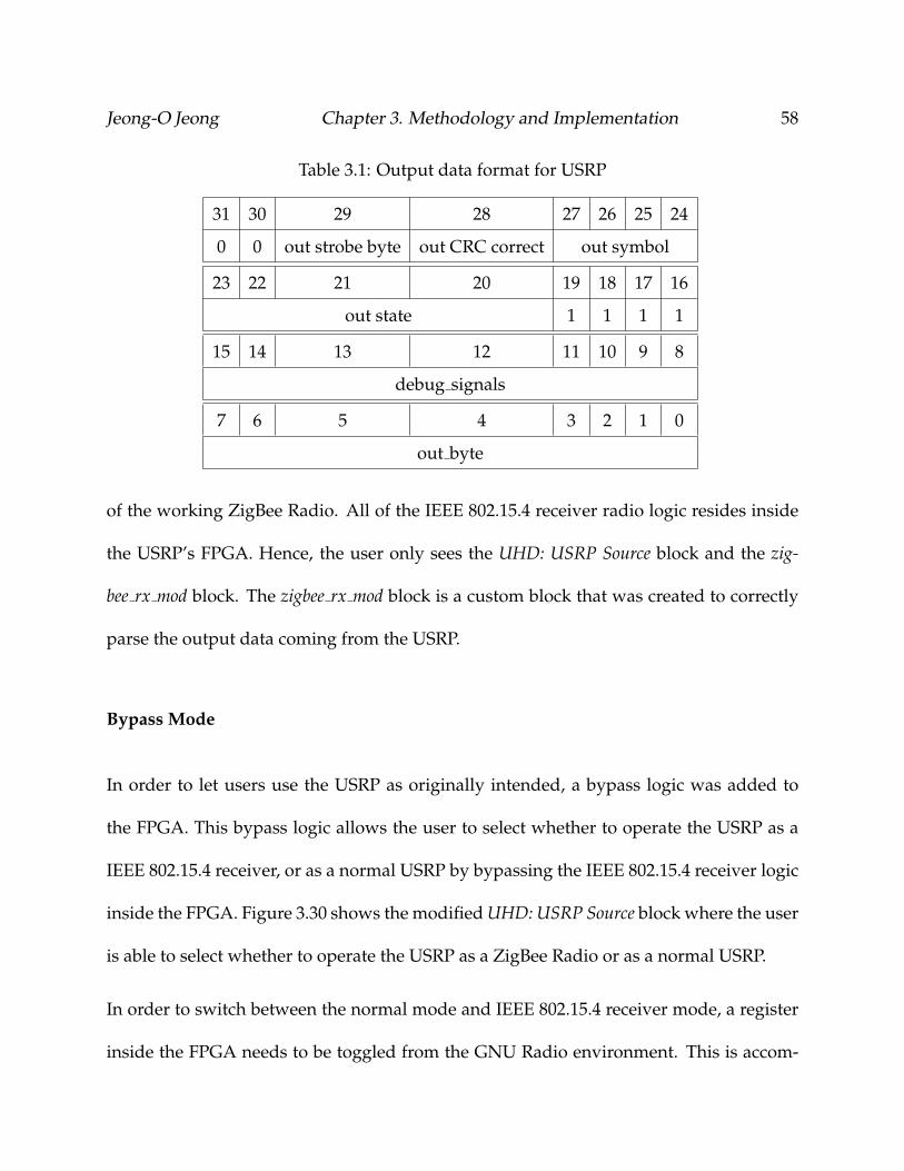
Jeong-O Jeong Chapter 3. Methodology and Implementation 58
Table 3.1: Output data format for USRP
31 30 29 28 27 26 25 24
0 0 out strobe byte out CRC correct out symbol
23 22 21 20 19 18 17 16
out state 1 1 1 1
15 14 13 12 11 10 9 8
debug signals
7 6 5 4 3 2 1 0
out byte
of the working ZigBee Radio. All of the IEEE 802.15.4 receiver radio logic resides inside
the USRP’s FPGA. Hence, the user only sees the UHD: USRP Source block and the zig-
bee rx mod block. The zigbee rx mod block is a custom block that was created to correctly
parse the output data coming from the USRP.
Bypass Mode
In order to let users use the USRP as originally intended, a bypass logic was added to
the FPGA. This bypass logic allows the user to select whether to operate the USRP as a
IEEE 802.15.4 receiver, or as a normal USRP by bypassing the IEEE 802.15.4 receiver logic
inside the FPGA. Figure 3.30 shows the modified UHD: USRP Source block where the user
is able to select whether to operate the USRP as a ZigBee Radio or as a normal USRP.
In order to switch between the normal mode and IEEE 802.15.4 receiver mode, a register
inside the FPGA needs to be toggled from the GNU Radio environment. This is accom-

Jeong-O Jeong Chapter 3. Methodology and Implementation 59
Figure 3.29: GNU Radio companion view of ZigBee RX
Figure 3.30: Modified UHD USRP Source Block
Jeong-O Jeong Chapter 3. Methodology and Implementation 60
plished by modifying the whole control chain that spans GNU Radio, UHD, and FPGA.
Figure 3.31 shows the series of modifications made to enable changing the register inside
the FPGA from a GNU Radio block.
Using the same logic for enabling the bypass mode, the thresholds for preamble and SFD
can be controlled also by changing the registers values inside the FPGA. Since usually
only a single receive channel dsp rx0 on the USRP is used, the registers in dsp rx1 were
re-routed to control the bypass register and the threshold registers.
3.2 Hybrid Multi-Channel IEEE 802.15.4 Receiver
3.2.1 Configuration
The hybrid implementation of multi-channel IEEE 802.15.4 receiver consists of three ma-
jor processing entities as shown in Figure 3.32: USRP N210, XUPV5, and GNU Radio.
The USRP acts as an RF front-end and a digital down converter. XUPV5 processes high
sample rate signal, and GNU Radio processes low sample rate signal. A channelizer re-
sides in XUPV5’s Virtex 5 FPGA to split a 20 MHz bandwidth signal into four 5 MHz
channels. An energy detector in the same FPGA then detects which channel is occupied
by the IEEE 802.15.4 transmitter. The energy detector then tells a 4:1 multiplexer to send
only the output of the occupied channel to GNU Radio. The IEEE 802.15.4 receiver in
GNU Radio then demodulates the received channel. When the transmitter switches to a
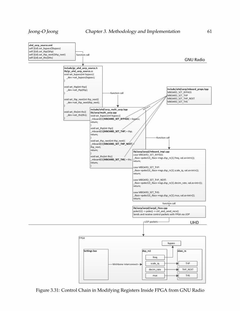
Jeong-O Jeong Chapter 3. Methodology and Implementation 61
Figure 3.31: Control Chain in Modifying Registers Inside FPGA from GNU Radio
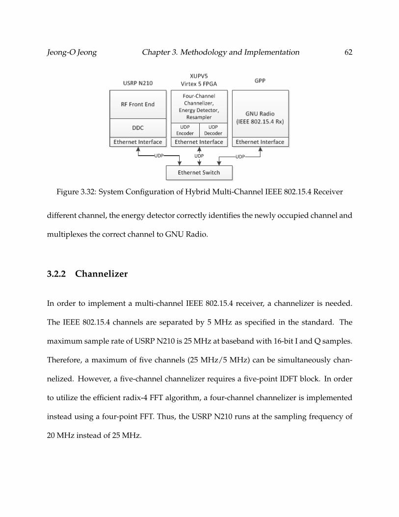
Jeong-O Jeong Chapter 3. Methodology and Implementation 62
Figure 3.32: System Configuration of Hybrid Multi-Channel IEEE 802.15.4 Receiver
different channel, the energy detector correctly identifies the newly occupied channel and
multiplexes the correct channel to GNU Radio.
3.2.2 Channelizer
In order to implement a multi-channel IEEE 802.15.4 receiver, a channelizer is needed.
The IEEE 802.15.4 channels are separated by 5 MHz as specified in the standard. The
maximum sample rate of USRP N210 is 25 MHz at baseband with 16-bit I and Q samples.
Therefore, a maximum of five channels (25 MHz/5 MHz) can be simultaneously chan-
nelized. However, a five-channel channelizer requires a five-point IDFT block. In order
to utilize the efficient radix-4 FFT algorithm, a four-channel channelizer is implemented
instead using a four-point FFT. Thus, the USRP N210 runs at the sampling frequency of
20 MHz instead of 25 MHz.
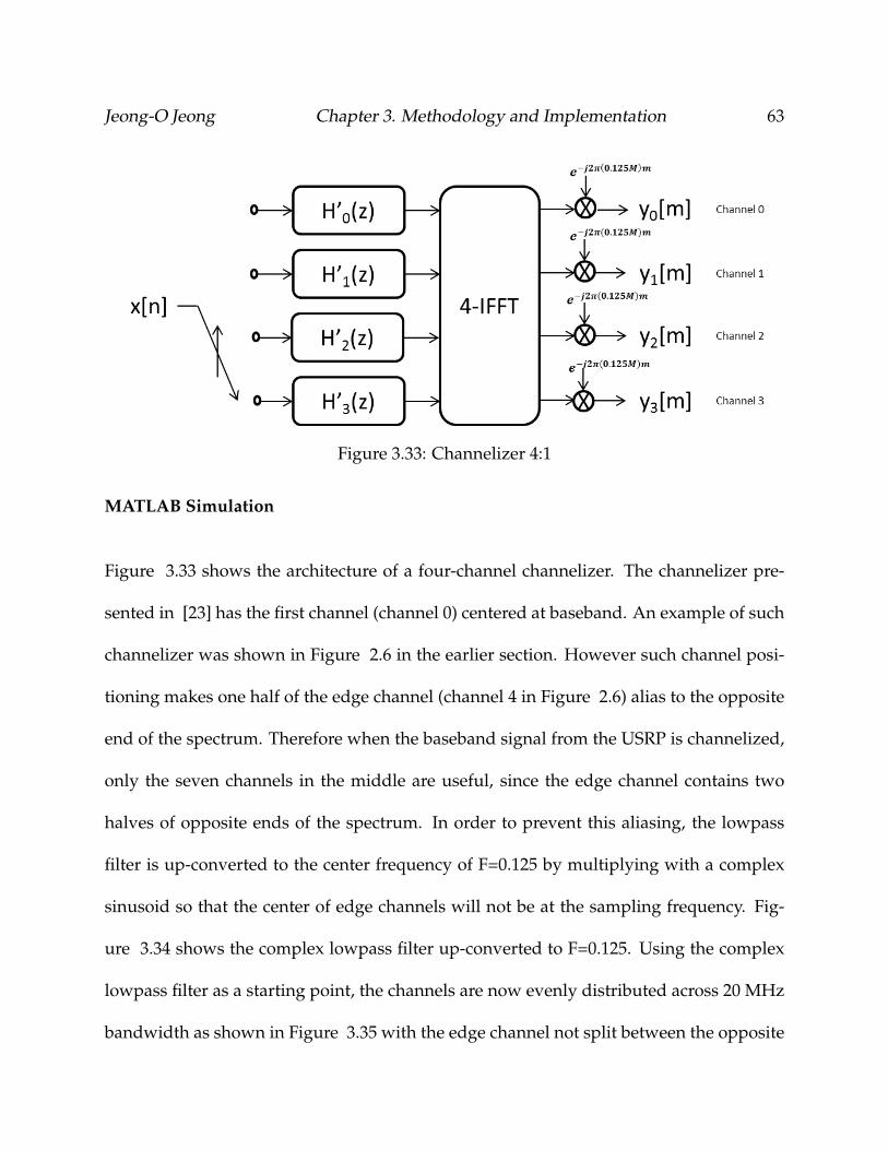
Jeong-O Jeong Chapter 3. Methodology and Implementation 63
Figure 3.33: Channelizer 4:1
MATLAB Simulation
Figure 3.33 shows the architecture of a four-channel channelizer. The channelizer pre-
sented in [23] has the first channel (channel 0) centered at baseband. An example of such
channelizer was shown in Figure 2.6 in the earlier section. However such channel posi-
tioning makes one half of the edge channel (channel 4 in Figure 2.6) alias to the opposite
end of the spectrum. Therefore when the baseband signal from the USRP is channelized,
only the seven channels in the middle are useful, since the edge channel contains two
halves of opposite ends of the spectrum. In order to prevent this aliasing, the lowpass
filter is up-converted to the center frequency of F=0.125 by multiplying with a complex
sinusoid so that the center of edge channels will not be at the sampling frequency. Fig-
ure 3.34 shows the complex lowpass filter up-converted to F=0.125. Using the complex
lowpass filter as a starting point, the channels are now evenly distributed across 20 MHz
bandwidth as shown in Figure 3.35 with the edge channel not split between the opposite
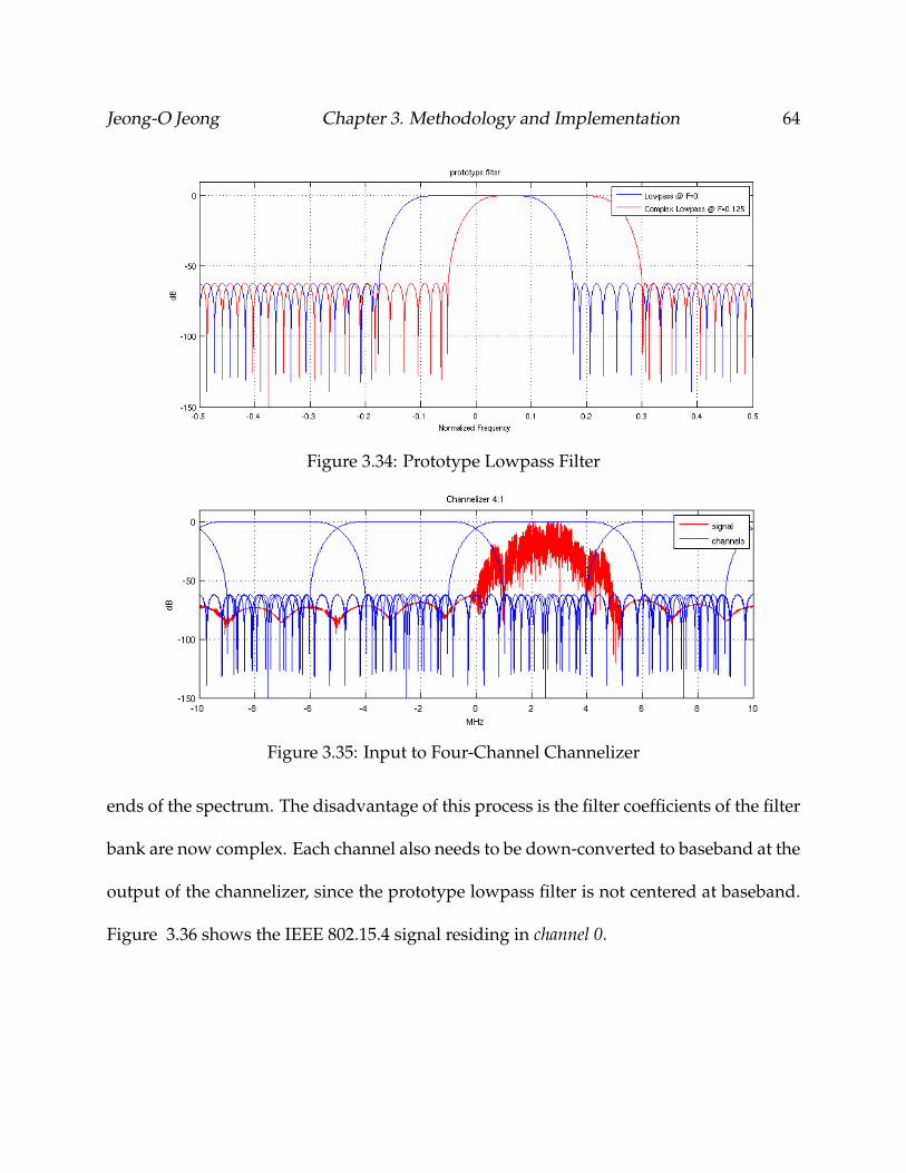
Jeong-O Jeong Chapter 3. Methodology and Implementation 64
Figure 3.34: Prototype Lowpass Filter
Figure 3.35: Input to Four-Channel Channelizer
ends of the spectrum. The disadvantage of this process is the filter coefficients of the filter
bank are now complex. Each channel also needs to be down-converted to baseband at the
output of the channelizer, since the prototype lowpass filter is not centered at baseband.
Figure 3.36 shows the IEEE 802.15.4 signal residing in channel 0.
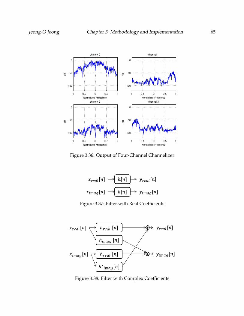
Jeong-O Jeong Chapter 3. Methodology and Implementation 65
Figure 3.36: Output of Four-Channel Channelizer
Figure 3.37: Filter with Real Coefficients
Figure 3.38: Filter with Complex Coefficients

Jeong-O Jeong Chapter 3. Methodology and Implementation 66
FPGA Implementation
Since the lowpass filter is up-converted to F=0.125, the coefficients of the new lowpass
filter are complex-valued. When a filter is real, the i-phase and q-phase parts of the signal
can be independently filtered as shown in Figure 3.37. However, when a filter is complex,
the i-phase and q-phase have to be both filtered by real and imaginary coefficients of the
filter and combined as shown in Figure 3.38. Therefore, complex filters require twice as
many resources as real filters.
Once the samples are filtered, they are input to the FFT block. The four-point FFT can be
easily built with the radix-4 FFT architecture. Since N=4, only a single radix-4 butterfly is
required. In matrix form, four-point DFT can be expressed as Equation 3.10.
X[0]
X[1]
X[2]
X[3]
=
1 1 1 1
1 −j −1 j
1 −1 1 −1
1 j −1 −j
×
x[0]
x[1]
x[2]
x[3]
(3.10)
The matrix equation can be simplified as Equation 3.11 which only consists of additions
and subtractions. Thus, using the radix-4 butterfly, the four-point FFT can be reduced to
Jeong-O Jeong Chapter 3. Methodology and Implementation 67
a series of simple additions and subtractions.
X(0) = x[0] + x[1] + x[2] + x[3] (3.11)
= xi[0] + xi[1] + xi[2] + xi[3] + j(xq[0] + xq[1] + xq[2] + xq[3])
X(1) = x[0]− jx[1]− x[2] + jx[3]
= xi[0] + xq[1]− xi[2]− xq[3] + j(xq[0]− xi[1]− xq[2] + xi[3])
X(2) = x[0]− x[1] + x[2]− x[3]
= xi[0]− xi[1] + xi[2]− xi[3] + j(xq[0]− xq[1] + xq[2]− xq[3])
X(3) = x[0] + jx[1]− x[2]− jx[3]
= xi[0]− xq[1]− xi[2] + xq[3] + j(xq[0] + xi[1]− xq[2]− xi[3])
After IFFT, each channel needs to be down-converted by F = 0.125M to compensate for
the up-converted lowpass filter. The down-conversion is achieved by multiplying each
channel with the complex sinusoid e−j2πM0.125(m) = e−j2π0.5(m). The complex sinusoid at
F=0.5 simplifies to 1,−1, 1,−1, 1.... Therefore, down-conversion for each channel simpli-
fies to flipping the sign of every other sample.

Jeong-O Jeong Chapter 3. Methodology and Implementation 68
Figure 3.39: Energy Detector
3.2.3 Energy Detector
FPGA Implementation
Figure 3.39 shows the energy detector to detect the channel where signal is present. The
average of four consecutive samples of magnitude of each channel is compared, and the
channel with most energy is sent through a multiplexer to the resampler.
3.2.4 Resampler 4/5
Since the sample rate of each channel is 5 MHz, a resampler is needed to convert the
sample rate to 4 MHz for the demodulator to work properly. A simple polyphase filter-
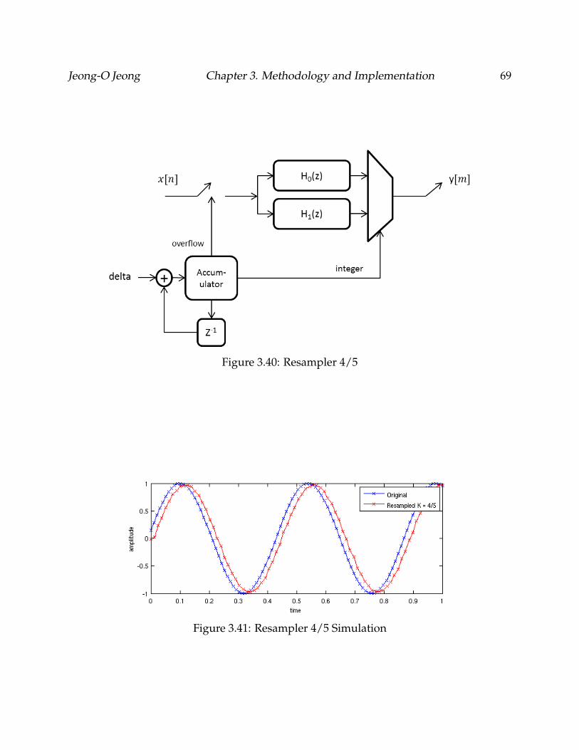
Jeong-O Jeong Chapter 3. Methodology and Implementation 69
Figure 3.40: Resampler 4/5
Figure 3.41: Resampler 4/5 Simulation
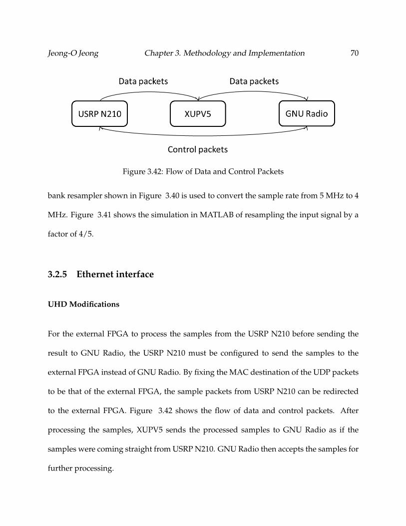
Jeong-O Jeong Chapter 3. Methodology and Implementation 70
Figure 3.42: Flow of Data and Control Packets
bank resampler shown in Figure 3.40 is used to convert the sample rate from 5 MHz to 4
MHz. Figure 3.41 shows the simulation in MATLAB of resampling the input signal by a
factor of 4/5.
3.2.5 Ethernet interface
UHD Modifications
For the external FPGA to process the samples from the USRP N210 before sending the
result to GNU Radio, the USRP N210 must be configured to send the samples to the
external FPGA instead of GNU Radio. By fixing the MAC destination of the UDP packets
to be that of the external FPGA, the sample packets from USRP N210 can be redirected
to the external FPGA. Figure 3.42 shows the flow of data and control packets. After
processing the samples, XUPV5 sends the processed samples to GNU Radio as if the
samples were coming straight from USRP N210. GNU Radio then accepts the samples for
further processing.
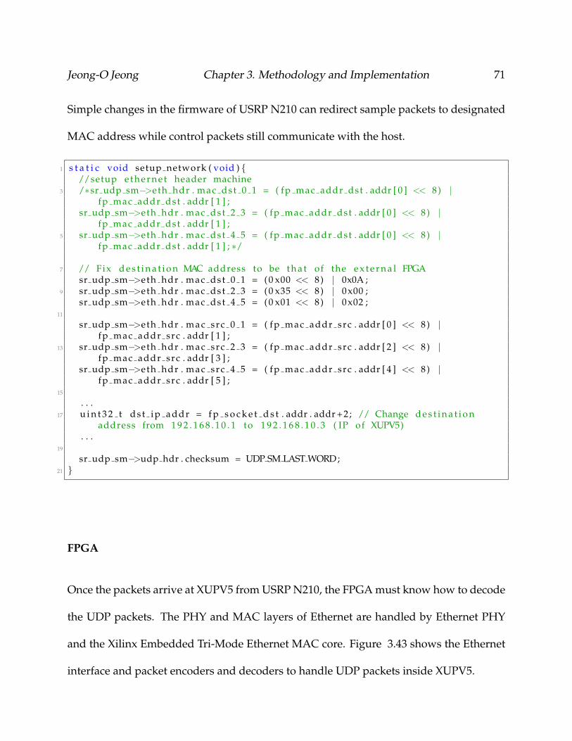
Jeong-O Jeong Chapter 3. Methodology and Implementation 71
Simple changes in the firmware of USRP N210 can redirect sample packets to designated
MAC address while control packets still communicate with the host.
1 s t a t i c void setup network ( void ) {//setup e t h e r n e t header machine
3 /∗sr udp sm−>eth hdr . mac dst 0 1 = ( fp mac addr dst . addr [ 0 ] << 8) |fp mac addr dst . addr [ 1 ] ;
sr udp sm−>eth hdr . mac dst 2 3 = ( fp mac addr dst . addr [ 0 ] << 8) |fp mac addr dst . addr [ 1 ] ;
5 sr udp sm−>eth hdr . mac dst 4 5 = ( fp mac addr dst . addr [ 0 ] << 8) |fp mac addr dst . addr [ 1 ] ; ∗/
7 // Fix d e s t i n a t i o n MAC address to be t h a t of the e x t e r n a l FPGAsr udp sm−>eth hdr . mac dst 0 1 = (0 x00 << 8) | 0x0A ;
9 sr udp sm−>eth hdr . mac dst 2 3 = (0 x35 << 8) | 0x00 ;sr udp sm−>eth hdr . mac dst 4 5 = (0 x01 << 8) | 0x02 ;
11
sr udp sm−>eth hdr . mac src 0 1 = ( fp mac addr src . addr [ 0 ] << 8) |fp mac addr src . addr [ 1 ] ;
13 sr udp sm−>eth hdr . mac src 2 3 = ( fp mac addr src . addr [ 2 ] << 8) |fp mac addr src . addr [ 3 ] ;
sr udp sm−>eth hdr . mac src 4 5 = ( fp mac addr src . addr [ 4 ] << 8) |fp mac addr src . addr [ 5 ] ;
15
. . .17 u i n t 3 2 t d s t i p a d d r = f p s o c k e t d s t . addr . addr +2; // Change d e s t i n a t i o n
address from 1 9 2 . 1 6 8 . 1 0 . 1 to 1 9 2 . 1 6 8 . 1 0 . 3 ( IP of XUPV5). . .
19
sr udp sm−>udp hdr . checksum = UDP SM LAST WORD;21 }
FPGA
Once the packets arrive at XUPV5 from USRP N210, the FPGA must know how to decode
the UDP packets. The PHY and MAC layers of Ethernet are handled by Ethernet PHY
and the Xilinx Embedded Tri-Mode Ethernet MAC core. Figure 3.43 shows the Ethernet
interface and packet encoders and decoders to handle UDP packets inside XUPV5.
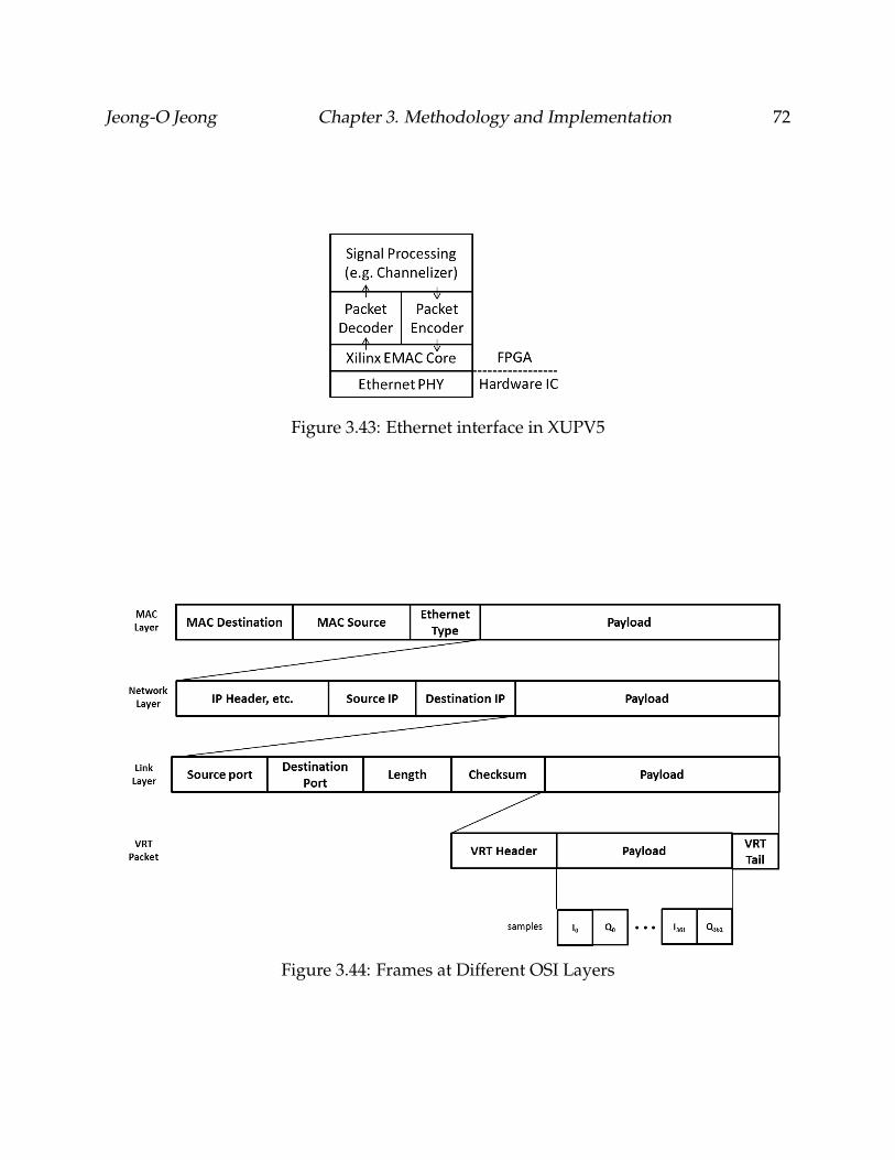
Jeong-O Jeong Chapter 3. Methodology and Implementation 72
Figure 3.43: Ethernet interface in XUPV5
Figure 3.44: Frames at Different OSI Layers
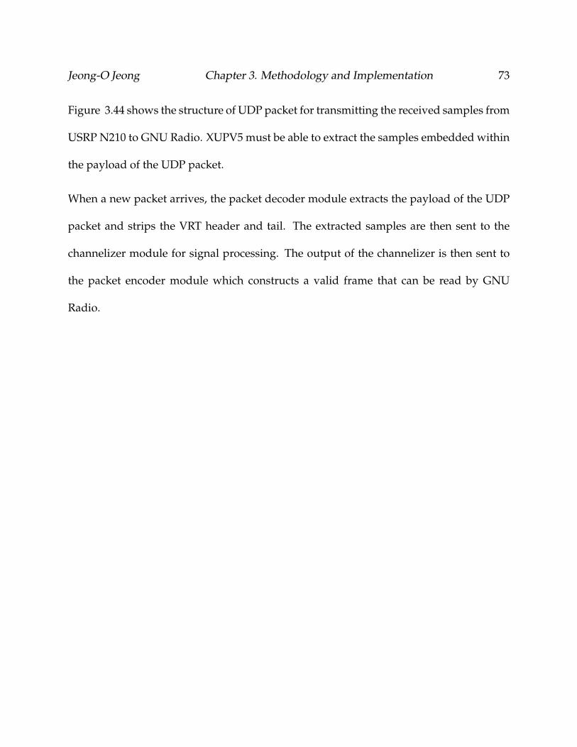
Jeong-O Jeong Chapter 3. Methodology and Implementation 73
Figure 3.44 shows the structure of UDP packet for transmitting the received samples from
USRP N210 to GNU Radio. XUPV5 must be able to extract the samples embedded within
the payload of the UDP packet.
When a new packet arrives, the packet decoder module extracts the payload of the UDP
packet and strips the VRT header and tail. The extracted samples are then sent to the
channelizer module for signal processing. The output of the channelizer is then sent to
the packet encoder module which constructs a valid frame that can be read by GNU
Radio.
Chapter 4
Results
4.1 Resource Utilization
The tables in this section show the resource utilizations of the FPGA implementations of
the IEEE 802.15.4 PHY and the multi-channel receiver. For the IEEE 802.15.4 PHY, the the
transmitter is implemented on USRP2, while the receiver is implemented on USRP N210.
The receiver is implemented on the USRP N210 instead of USRP2 because the latter does
not have enough resources to support signal processing for the receiver algorithm.
4.1.1 Transmitter
Table 4.1 shows the resource utilization of the IEEE 802.15.4 transmitter by itself. No
multiplier is used for the transmitter even though the transmitter core has a half-sin pulse
74
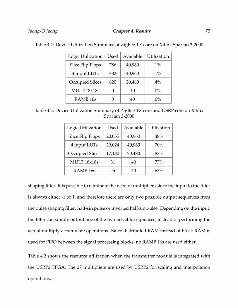
Jeong-O Jeong Chapter 4. Results 75
Table 4.1: Device Utilization Summary of ZigBee TX core on Xilinx Spartan 3-2000
Logic Utilization Used Available Utilization
Slice Flip Flops 786 40,960 1%
4 input LUTs 782 40,960 1%
Occupied Slices 820 20,480 4%
MULT 18x18s 0 40 0%
RAMB 16s 0 40 0%
Table 4.2: Device Utilization Summary of ZigBee TX core and USRP core on XilinxSpartan 3-2000
Logic Utilization Used Available Utilization
Slice Flip Flops 20,055 40,960 48%
4 input LUTs 29,024 40,960 70%
Occupied Slices 17,130 20,480 83%
MULT 18x18s 31 40 77%
RAMB 16s 25 40 63%
shaping filter. It is possible to eliminate the need of multipliers since the input to the filter
is always either -1 or 1, and therefore there are only two possible output sequences from
the pulse shaping filter: half-sin pulse or inverted half-sin pulse. Depending on the input,
the filter can simply output one of the two possible sequences, instead of performing the
actual multiply-accumulate operations. Since distributed RAM instead of block RAM is
used for FIFO between the signal processing blocks, no RAMB 16s are used either.
Table 4.2 shows the resource utilization when the transmitter module is integrated with
the USRP2 FPGA. The 27 multipliers are used by USRP2 for scaling and interpolation
operations.
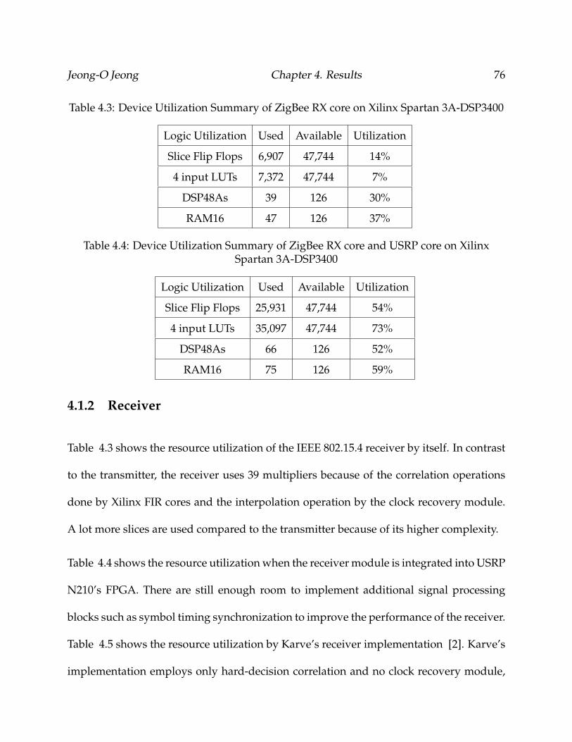
Jeong-O Jeong Chapter 4. Results 76
Table 4.3: Device Utilization Summary of ZigBee RX core on Xilinx Spartan 3A-DSP3400
Logic Utilization Used Available Utilization
Slice Flip Flops 6,907 47,744 14%
4 input LUTs 7,372 47,744 7%
DSP48As 39 126 30%
RAM16 47 126 37%
Table 4.4: Device Utilization Summary of ZigBee RX core and USRP core on XilinxSpartan 3A-DSP3400
Logic Utilization Used Available Utilization
Slice Flip Flops 25,931 47,744 54%
4 input LUTs 35,097 47,744 73%
DSP48As 66 126 52%
RAM16 75 126 59%
4.1.2 Receiver
Table 4.3 shows the resource utilization of the IEEE 802.15.4 receiver by itself. In contrast
to the transmitter, the receiver uses 39 multipliers because of the correlation operations
done by Xilinx FIR cores and the interpolation operation by the clock recovery module.
A lot more slices are used compared to the transmitter because of its higher complexity.
Table 4.4 shows the resource utilization when the receiver module is integrated into USRP
N210’s FPGA. There are still enough room to implement additional signal processing
blocks such as symbol timing synchronization to improve the performance of the receiver.
Table 4.5 shows the resource utilization by Karve’s receiver implementation [2]. Karve’s
implementation employs only hard-decision correlation and no clock recovery module,
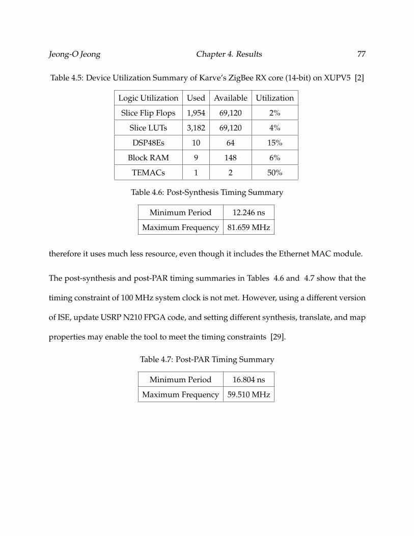
Jeong-O Jeong Chapter 4. Results 77
Table 4.5: Device Utilization Summary of Karve’s ZigBee RX core (14-bit) on XUPV5 [2]
Logic Utilization Used Available Utilization
Slice Flip Flops 1,954 69,120 2%
Slice LUTs 3,182 69,120 4%
DSP48Es 10 64 15%
Block RAM 9 148 6%
TEMACs 1 2 50%
Table 4.6: Post-Synthesis Timing Summary
Minimum Period 12.246 ns
Maximum Frequency 81.659 MHz
therefore it uses much less resource, even though it includes the Ethernet MAC module.
The post-synthesis and post-PAR timing summaries in Tables 4.6 and 4.7 show that the
timing constraint of 100 MHz system clock is not met. However, using a different version
of ISE, update USRP N210 FPGA code, and setting different synthesis, translate, and map
properties may enable the tool to meet the timing constraints [29].
Table 4.7: Post-PAR Timing Summary
Minimum Period 16.804 ns
Maximum Frequency 59.510 MHz
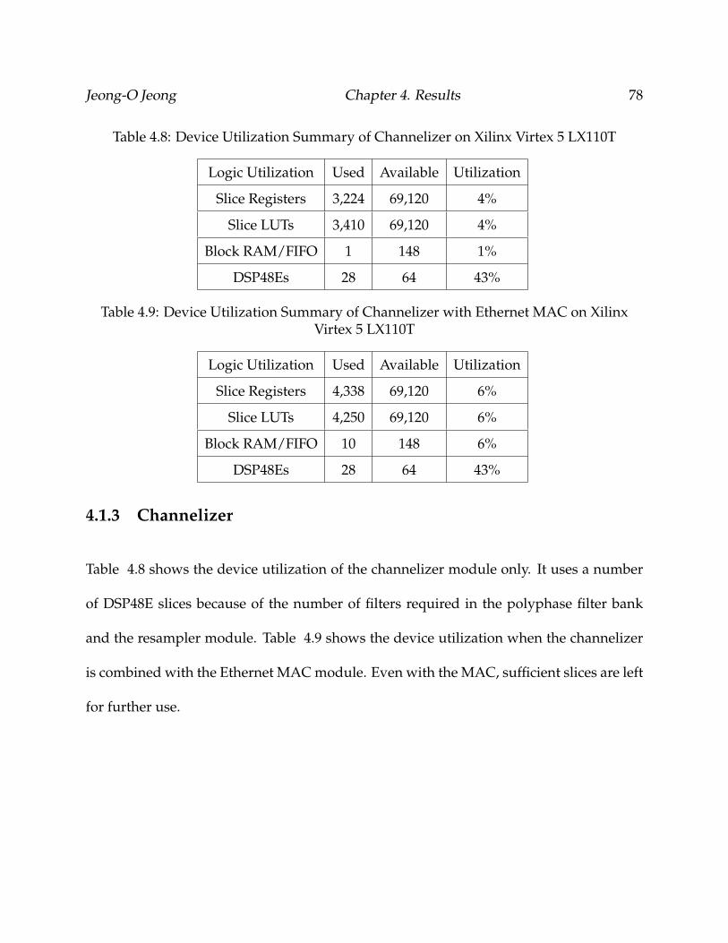
Jeong-O Jeong Chapter 4. Results 78
Table 4.8: Device Utilization Summary of Channelizer on Xilinx Virtex 5 LX110T
Logic Utilization Used Available Utilization
Slice Registers 3,224 69,120 4%
Slice LUTs 3,410 69,120 4%
Block RAM/FIFO 1 148 1%
DSP48Es 28 64 43%
Table 4.9: Device Utilization Summary of Channelizer with Ethernet MAC on XilinxVirtex 5 LX110T
Logic Utilization Used Available Utilization
Slice Registers 4,338 69,120 6%
Slice LUTs 4,250 69,120 6%
Block RAM/FIFO 10 148 6%
DSP48Es 28 64 43%
4.1.3 Channelizer
Table 4.8 shows the device utilization of the channelizer module only. It uses a number
of DSP48E slices because of the number of filters required in the polyphase filter bank
and the resampler module. Table 4.9 shows the device utilization when the channelizer
is combined with the Ethernet MAC module. Even with the MAC, sufficient slices are left
for further use.
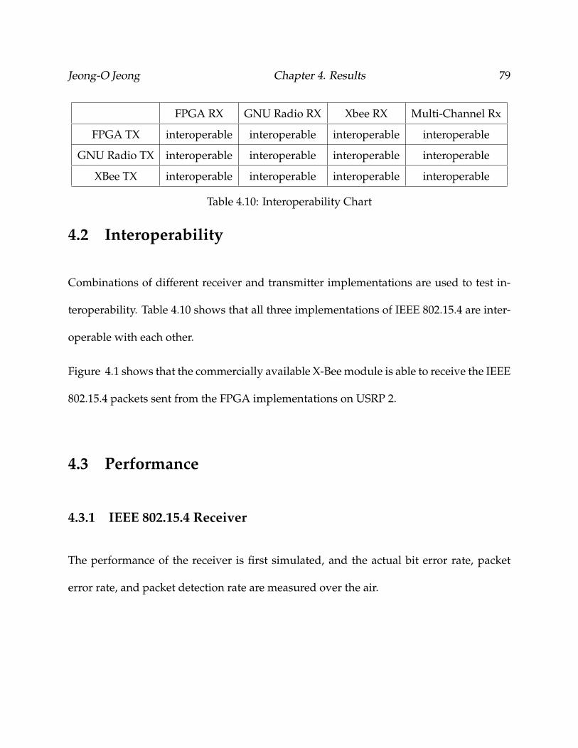
Jeong-O Jeong Chapter 4. Results 79
FPGA RX GNU Radio RX Xbee RX Multi-Channel Rx
FPGA TX interoperable interoperable interoperable interoperable
GNU Radio TX interoperable interoperable interoperable interoperable
XBee TX interoperable interoperable interoperable interoperable
Table 4.10: Interoperability Chart
4.2 Interoperability
Combinations of different receiver and transmitter implementations are used to test in-
teroperability. Table 4.10 shows that all three implementations of IEEE 802.15.4 are inter-
operable with each other.
Figure 4.1 shows that the commercially available X-Bee module is able to receive the IEEE
802.15.4 packets sent from the FPGA implementations on USRP 2.
4.3 Performance
4.3.1 IEEE 802.15.4 Receiver
The performance of the receiver is first simulated, and the actual bit error rate, packet
error rate, and packet detection rate are measured over the air.

Jeong-O Jeong Chapter 4. Results 80
Figure 4.1: Message from FPGA received by Xbee console
Simulation
Figure 4.2 shows the chip error rate of O-QPSK signal. The theoretical curve is simply the
bit error rate curve of the O-QPSK modulation. The simulation of O-QPSK demodulation
very closely matches the theoretical curve. As expected, differential demodulation using
the delay-conjugate-multiply scheme results in poorer performance. However, matched-
filtering the input signal with half-sine pulse shape increases the performance of the dif-
ferential demodulation. The simulation done in Karve’s thesis is also shown [2]. All
simulations assume perfect synchronization. Figure 4.3 shows the simulated BER curves.
The “Coherent Demodulation” curve assumes perfect receiver synchronization. The O-
QPSK chips are demodulated coherently and then despread to recover the information
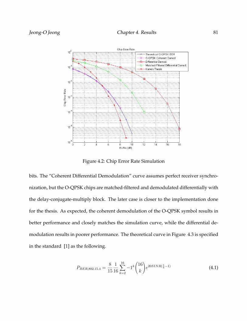
Jeong-O Jeong Chapter 4. Results 81
Figure 4.2: Chip Error Rate Simulation
bits. The “Coherent Differential Demodulation” curve assumes perfect receiver synchro-
nization, but the O-QPSK chips are matched-filtered and demodulated differentially with
the delay-conjugate-multiply block. The later case is closer to the implementation done
for the thesis. As expected, the coherent demodulation of the O-QPSK symbol results in
better performance and closely matches the simulation curve, while the differential de-
modulation results in poorer performance. The theoretical curve in Figure 4.3 is specified
in the standard [1] as the following.
PBER,802.15.4 =8
15
1
16
16∑k=2
−1k(
16
k
)e20SINR( 1
k−1) (4.1)
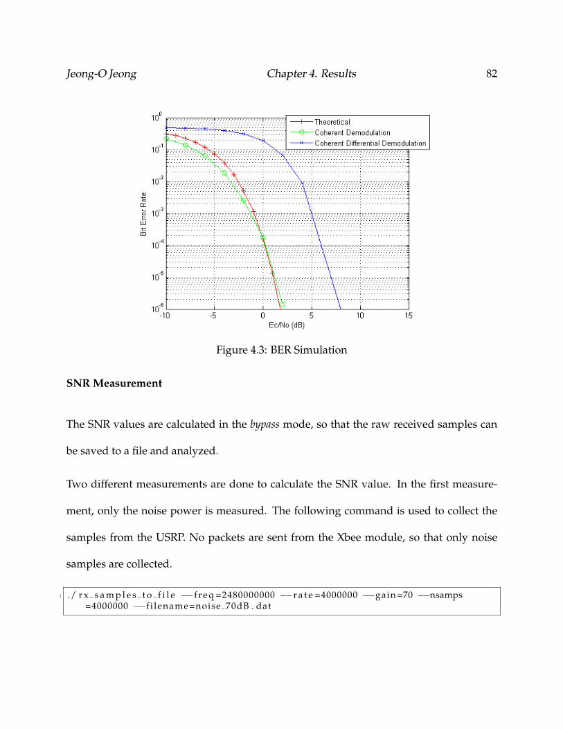
Jeong-O Jeong Chapter 4. Results 82
Figure 4.3: BER Simulation
SNR Measurement
The SNR values are calculated in the bypass mode, so that the raw received samples can
be saved to a file and analyzed.
Two different measurements are done to calculate the SNR value. In the first measure-
ment, only the noise power is measured. The following command is used to collect the
samples from the USRP. No packets are sent from the Xbee module, so that only noise
samples are collected.
1 ./ r x s a m p l e s t o f i l e −−f r e q =2480000000 −−r a t e =4000000 −−gain =70 −−nsamps=4000000 −−f i lename=noise 70dB . dat

Jeong-O Jeong Chapter 4. Results 83
Figure 4.4: Received Packets in Time Domain
In the second measurement, the packets are sent from the XBee module so that the signal
of interest as well as the noise samples are captured. The gain on the receiver is set to be
the same so that the noise power is the same as in the first measurement.
1 ./ r x s a m p l e s t o f i l e −−f r e q =2480000000 −−r a t e =4000000 −−gain =70 −−nsamps=4000000 −−f i lename=signal 70dB . dat
Figure 4.4 shows one instance of the second measurement, where two packets are clearly
seen. The following equation is used to calculate the SNR from the two measurements.
S
N=PsignalPnoise
(4.2)
EbN0
=S
N(4.3)
Jeong-O Jeong Chapter 4. Results 84
Etotal =N−1∑
0
|x[n]|2 (4.4)
= PsignalNsignal + PnoiseNnoise
where N = Nsignal + Nnoise is the total number of samples, Nsignal is the number of signal
samples, and Nnoise is the number of noise samples. In the first measurement, since there
is no signal present, the equation can be re-written as the following.
Etotal =N−1∑
0
|x[n]|2 (4.5)
= PnoiseNnoise
= PnoiseN
Solving for Pnoise, the noise power can be calculated.
Pnoise =
∑ |x[n]|2
Nnoise
(4.6)
=∑|x[n]|2/N
(4.7)
In Equation 4.4, Nsignal is known because the number of packets and the length of each
packet can be controlled. Psignal is then the following.
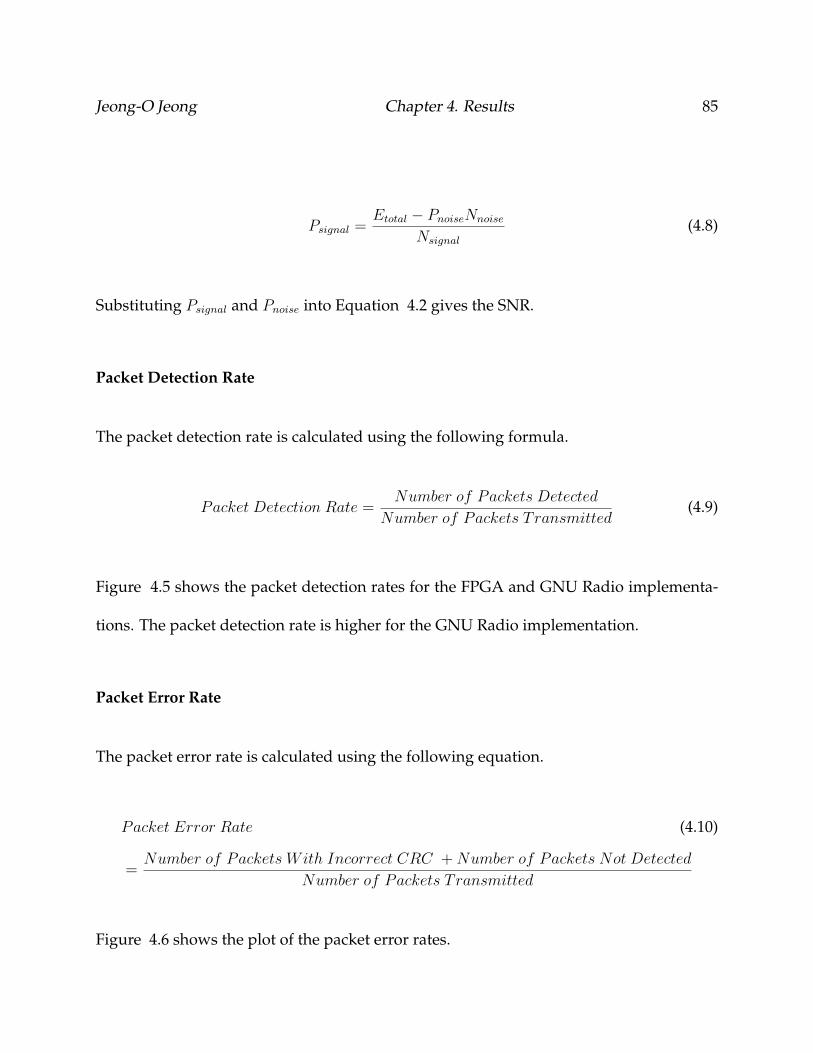
Jeong-O Jeong Chapter 4. Results 85
Psignal =Etotal − PnoiseNnoise
Nsignal
(4.8)
Substituting Psignal and Pnoise into Equation 4.2 gives the SNR.
Packet Detection Rate
The packet detection rate is calculated using the following formula.
Packet Detection Rate =Number of Packets Detected
Number of Packets Transmitted(4.9)
Figure 4.5 shows the packet detection rates for the FPGA and GNU Radio implementa-
tions. The packet detection rate is higher for the GNU Radio implementation.
Packet Error Rate
The packet error rate is calculated using the following equation.
Packet Error Rate (4.10)
=Number of Packets With Incorrect CRC +Number of Packets Not Detected
Number of Packets Transmitted
Figure 4.6 shows the plot of the packet error rates.

Jeong-O Jeong Chapter 4. Results 86
Figure 4.5: Percentages of Packets Detected
Figure 4.6: Packet Error Rate
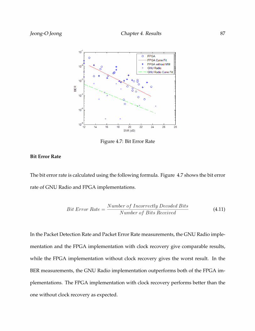
Jeong-O Jeong Chapter 4. Results 87
Figure 4.7: Bit Error Rate
Bit Error Rate
The bit error rate is calculated using the following formula. Figure 4.7 shows the bit error
rate of GNU Radio and FPGA implementations.
Bit Error Rate =Number of Incorrectly Decoded Bits
Number of Bits Received(4.11)
In the Packet Detection Rate and Packet Error Rate measurements, the GNU Radio imple-
mentation and the FPGA implementation with clock recovery give comparable results,
while the FPGA implementation without clock recovery gives the worst result. In the
BER measurements, the GNU Radio implementation outperforms both of the FPGA im-
plementations. The FPGA implementation with clock recovery performs better than the
one without clock recovery as expected.
Jeong-O Jeong Chapter 4. Results 88
Figure 4.8: Output of Inverse Tangent with Correct Sign
There are multiple reasons why the GNU Radio implementation outperforms the FPGA
implementation.
• Algorithmic
The output of the inverse tangent in the FPGA implementation is intentionally
set to zero when it is outside [−π/2,π/2], with some headroom, to decrease the corre-
lation value when noise is present. The rationale behind this is that when the signal
is present, the output of inverse tangent should be within [−π/4,π/4], and when
only noise is present, the output of inverse tangent is outside [−π/4,π/4]. By setting
the values outside the range to be zero, the correlation values are lower when only
noise is present, thereby decreasing the false alarm rate. However, at low SNR, the
output of inverse tangent is outside the range of [−π/2,π/2] even when the signal is
present. Therefore, the algorithm falsely decides that there is only noise present and

Jeong-O Jeong Chapter 4. Results 89
Figure 4.9: Output of Inverse Tangent with Mismatched Sign
Figure 4.10: Output of Inverse Tangent with Increased CORDIC Iterations
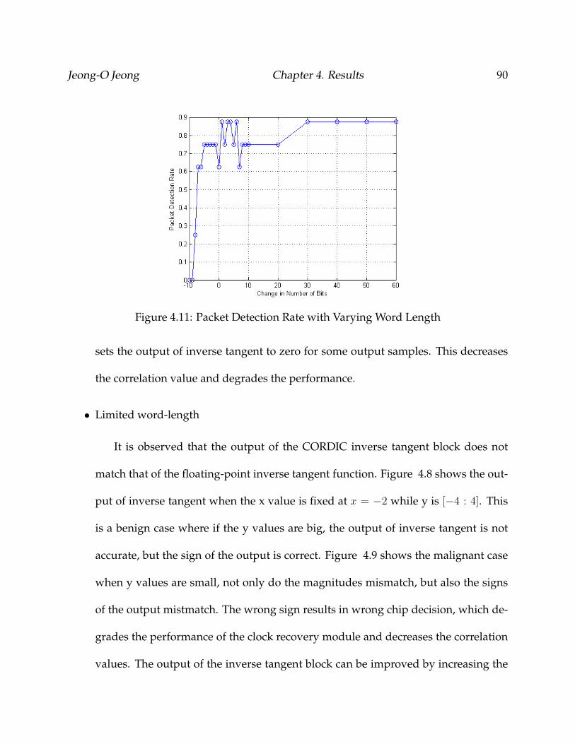
Jeong-O Jeong Chapter 4. Results 90
Figure 4.11: Packet Detection Rate with Varying Word Length
sets the output of inverse tangent to zero for some output samples. This decreases
the correlation value and degrades the performance.
• Limited word-length
It is observed that the output of the CORDIC inverse tangent block does not
match that of the floating-point inverse tangent function. Figure 4.8 shows the out-
put of inverse tangent when the x value is fixed at x = −2 while y is [−4 : 4]. This
is a benign case where if the y values are big, the output of inverse tangent is not
accurate, but the sign of the output is correct. Figure 4.9 shows the malignant case
when y values are small, not only do the magnitudes mismatch, but also the signs
of the output mistmatch. The wrong sign results in wrong chip decision, which de-
grades the performance of the clock recovery module and decreases the correlation
values. The output of the inverse tangent block can be improved by increasing the
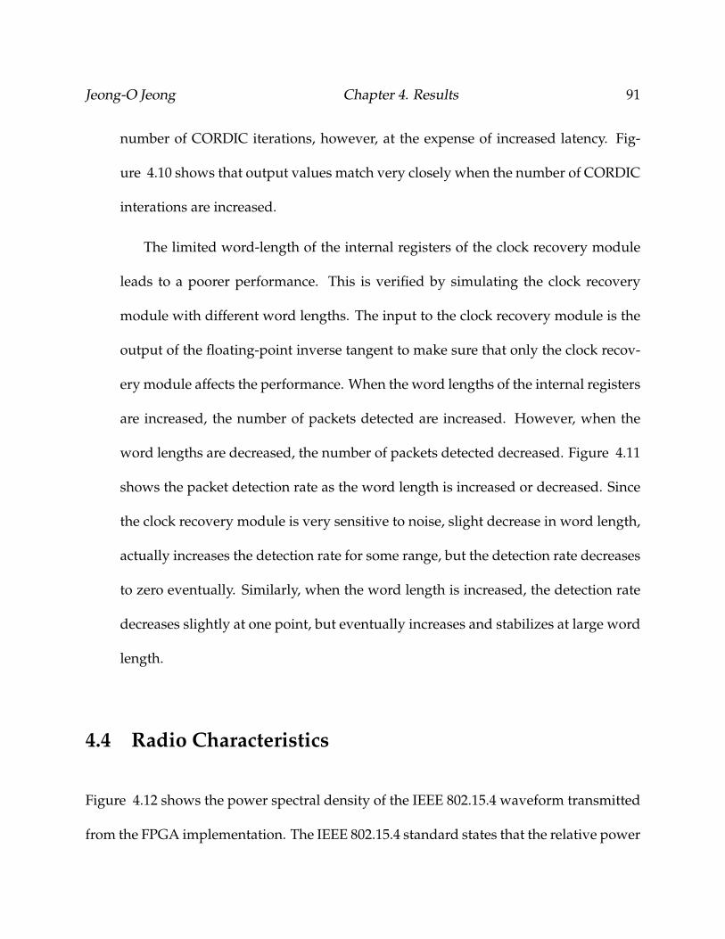
Jeong-O Jeong Chapter 4. Results 91
number of CORDIC iterations, however, at the expense of increased latency. Fig-
ure 4.10 shows that output values match very closely when the number of CORDIC
interations are increased.
The limited word-length of the internal registers of the clock recovery module
leads to a poorer performance. This is verified by simulating the clock recovery
module with different word lengths. The input to the clock recovery module is the
output of the floating-point inverse tangent to make sure that only the clock recov-
ery module affects the performance. When the word lengths of the internal registers
are increased, the number of packets detected are increased. However, when the
word lengths are decreased, the number of packets detected decreased. Figure 4.11
shows the packet detection rate as the word length is increased or decreased. Since
the clock recovery module is very sensitive to noise, slight decrease in word length,
actually increases the detection rate for some range, but the detection rate decreases
to zero eventually. Similarly, when the word length is increased, the detection rate
decreases slightly at one point, but eventually increases and stabilizes at large word
length.
4.4 Radio Characteristics
Figure 4.12 shows the power spectral density of the IEEE 802.15.4 waveform transmitted
from the FPGA implementation. The IEEE 802.15.4 standard states that the relative power

Jeong-O Jeong Chapter 4. Results 92
Figure 4.12: Spectral Mask of IEEE 802.15.4 transmitted using USRP N210 FPGA
in frequency |f − fc| > 3.5MHz shall be less than -20 dBr compared to the average spec-
trałpower measured within ±1MHz of the carrier frequency. The measurement shall be
made using a 100 kHz resolution bandwidth. Figure 4.12 shows that power in the upper
and lower bands 3.5 MHz away from the center frequencies are -30.47 dB and -29.81 dB,
which satisfies the requirement.
The standards states that the transmitted center frequency tolerance shall be ±40ppm =
0.004%. Figure 4.13 shows that the frequency deviation is about 2.480008492 GHz − 2.48 GHz2.48 GHz
=
0.0003%, which lies within the tolerance limit.
The 99% occupied bandwidth is approximately 2 MHz as shown in Figure 4.14.
Figure 4.15 shows the constellation plot of the O-QPSK signal transmitted by the USRP
N210 FPGA implementation. As expected of O-QPSK signals, the constellation points do
not travel across the origin.
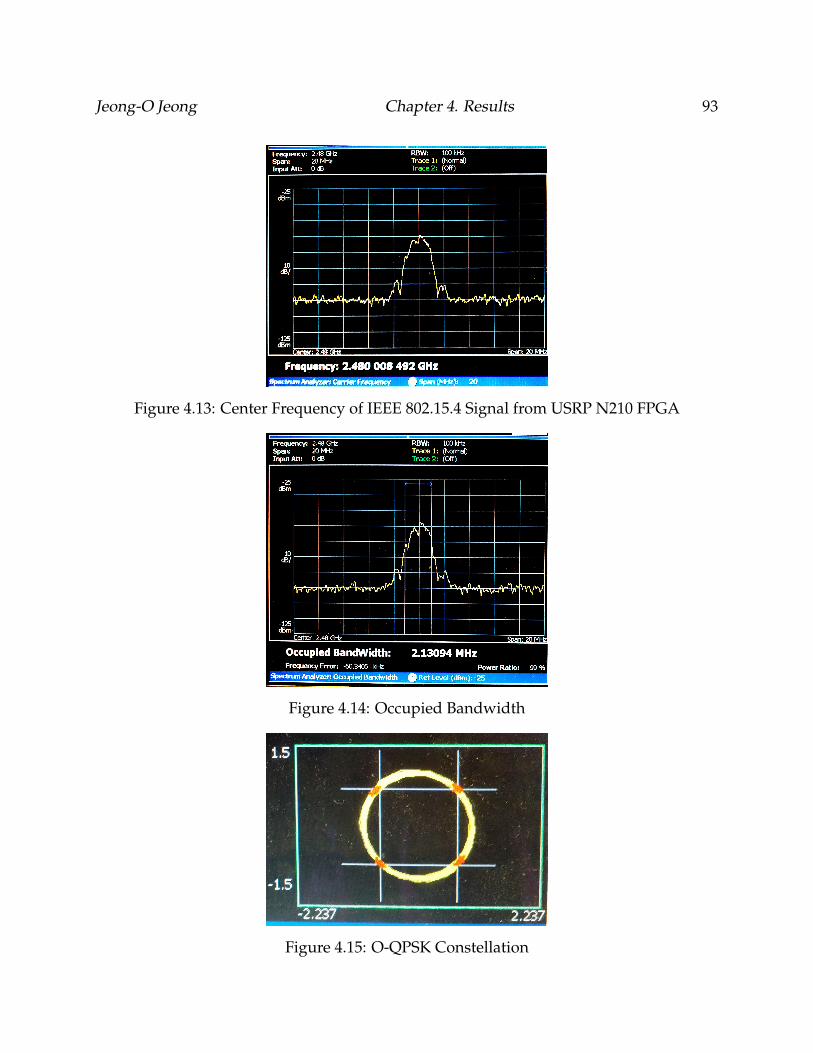
Jeong-O Jeong Chapter 4. Results 93
Figure 4.13: Center Frequency of IEEE 802.15.4 Signal from USRP N210 FPGA
Figure 4.14: Occupied Bandwidth
Figure 4.15: O-QPSK Constellation

Chapter 5
Conclusion and Future Work
Two different versions of IEEE 802.15.4 PHY implementations have been explored. The
first implementation demonstrates how a signal processing application such as IEEE 802.15.4
PHY can be embedded inside the USRP N210’s FPGA. This enables developers to take
advantage of the spare resources in the USRP N210’s FPGA and delegate complex signal
processing tasks from slow GPP to fast FPGA. GNU Radio is now free to do much more
processing since FPGA takes care of all the complex tasks.
The second implementation demonstrates the use of an external FPGA in the USRP and
GNU Radio environment. By modifying the firmware inside the USRP N210, it is possi-
ble to redirect packets from USRP N210 to the external FPGA. The external FPGA then
extracts the samples from the UDP packets and performs signal processing on the sam-
ples. Because external FPGAs can be much larger than USRP’s FPGA, even more complex
94
Jeong-O Jeong Chapter 5. Conclusion and Future Work 95
tasks can be performed on it. The example implementation of the multi-channel IEEE
802.15.4 demonstrates the viability of the platform by successfully decoding packets from
commercially available IEEE 802.15.4 node. If desired, a signal processing chain can be
distributed among all three platforms, the USRP’s FPGA, an external FPGA, and GNU
Radio. This platform is also extensible to additional external FPGAs if desired. The first
FPGA can process the samples from USRP and relay to the next FPGA, and so on, until
the result reaches GNU Radio.
Future work includes implementing a more complex signal processing applications such
as spectrum sensing algorithms or IEEE 802.11a.

Bibliography
[1] IEEE Std 802.15.4-2006, IEEE Std.
[2] M. P. Karve, “Evaluation of gnu radio platform enhanced for hardware accelerated
radio design,” Ph.D. dissertation, Virginia Polytechnic Institute and State University,
2010.
[3] D. Bursky. (2006, May) Designers stretched in asic, fpga tug-of-war. [On-
line]. Available: http://www.eetimes.com/design/automotive-design/4004080/
Designers-stretched-in-ASIC-FPGA-tug-of-war
[4] C. R. Irick, “Enhancing gnu radio for hardware accelerated radio design,” Ph.D. dis-
sertation, Virginia Polytechnic Institute and State University, 2010.
[5] K. Tan, J. Zhang, J. Fang, H. Liu, Y. Ye, S. Wang, Y. Zhang, H. Wu, W. Wang, and
G. M. Voelker, “Sora: High performance software radio using general purpose multi-
core processors,” NSDI 09: 6th USENIX Symposium on Networked Systems Design and
Implementation, 2009.
96
[6] A. T. Tran, D. N. Truong, and B. M. Baas, “A complete real-time 802.11a baseband
receiver implemented on an array of programmable processors,” Signals, Systems and
Computers, 2008 42nd Asilomar Conference on, pp. 165–170, 2008.
[7] J. H. Reed, Software Radio - A Modern Approach to Radio Engineering. PEARSON
Education, 2006.
[8] D. Lau, J. Blackburn, and J. A. Seely, “The use of hardware acceleration in sdr wave-
forms,” Altera Corporation, Tech. Rep., 2005.
[9] Intel. (2003) Intel hyper-threading technology. Intel. [Online]. Available: http:
//cache-www.intel.com/cd/00/00/01/77/17705 htt user guide.pdf
[10] Fftw. http://www.fftw.org/.
[11] T. Rondeau. (2010, 12) Volk: Vector-optimized library of kernels.
GNU Radio. [Online]. Available: http://www.trondeau.com/blog/2010/12/
11/volk-vector-optimized-library-of-kernels.html
[12] T. Schmid, “Gnu radio 802.15.4 en- and decoding,” NESL Department of Electrical
Engineering University of California, Los Angeles, Tech. Rep., 2006.
[13] M. A. R. Saghir, P. Chow, and C. G. Lee. (1998) A comparison of traditional and vliw
dsp architectures for compiled dsp applications. University of Toronto. [Online].
Available: www.eecg.toronto.edu/∼saghir/papers/CASES98.ps
97
[14] D. Liu, Embedded DSP Processor Design: Application Specific Instruction Set Processors.
Morgan Kaufmann, 2008.
[15] Altera. (2001) Fpgas provide reconfigurable dsp solutions. [Online]. Available:
http://www.altera.com/literature/wp/wp dsp fpga.pdf
[16] Xilinx. (2012, January) Virtex-5 fpga xtremedsp design considerations. [Online].
Available: http://www.xilinx.com/support/documentation/user guides/ug193.
[17] R. P. Brent, F. T. Luk, and C. V. Loan, “Computation of the singular value decompo-
sition using mesh-connected processors,” Journal of VLSI and Computer Systems, pp.
242–270, 1985.
[18] AccelChip. Using fpgas to improve the performance of radar, navigation and guid-
ance systems. [Online]. Available: http://www.design-reuse.com/articles/11366/
using-fpgas-to-improve-the-performance-of-radar-navigation-and-guidance-systems.
html
[19] I. Berkeley Design Technology. (2010) High-level synthesis tools for xilinx fpgas.
Berkeley Design Technology, Inc. [Online]. Available: www.bdti.com/MyBDTI/
pubs/Xilinx hlstcp.pdf
[20] ——. (2007, January) Fpgas vs. dsps: A look at the unanswered questions.
[Online]. Available: http://www.eetimes.com/design/signal-processing-dsp/
4017003/FPGAs-vs-DSPs-A-look-at-the-unanswered-questions/
98

[21] D. Gislason, ZigBee Wireless Networking. Newnes, 2008.
[22] E. Research. Ettus research. [Online]. Available: http://ettus.com/
[23] fredric j harris, Multirate Signal Processing For Communication Systems. Prentice Hall,
2004.
[24] J. Notor, A. Caviglia, and G. Levy. (2003) Cmos rfic architectures for ieee
802.15.4 networks. Cadence Design Systems, Inc. 6210 Old Dobbin Lane, Suite
100 Columbia, Maryland 21045, USA. [Online]. Available: http://chipbook.com/
databook/Interface/ZIGBEE/CMOSRFICArchforIEEE80215.pdf
[25] H. Meyr, M. Moeneclaey, and S. A. Fechtel, Digital Communication Receivers. John
Wiley & Sons, 1998.
[26] S. B. Wicker, Error Control Systems. Prentice Hall, 1995.
[27] K. Sankar. (2008, March) Frequency offset estimation using 802.11a
short preamble. [Online]. Available: http://www.dsplog.com/2008/03/03/
frequency-offset-estimation-using-80211a-short-preamble/
[28] MathWorks. Simulink hdl coder. MathWorks. [Online]. Available: http://www.
mathworks.com/products/slhdlcoder/
[29] J. Blum. (2012, May) Usrp users mailing list – universal software radio peripheral
by ettus research. [Online]. Available: http://comments.gmane.org/gmane.comp.
hardware.usrp.e100/3719
99

Appendix A
Verilog Source Code for IEEE 802.15.4Receiver on USRP N210’s FPGA
A.1 Receiver Top Level
1 ‘ t i m e s c a l e 1 ns / 1 ns/////////////////////////////////////////////////////////////////////////////
3 // Company : Wireless @ VT// Author : Jeong−O Jeong
5 //// Date : 1 6 : 4 1 : 4 8 12/17/2011
7 // Design Name:// Filename : xbee rx . v
9 // P r o j e c t Name:// Target Devices :
11 // Tool vers ions :// Descr ipt ion : Top f i l e f o r the IEEE 8 0 2 . 1 5 . 4 r e c e i v e r
13 //// Dependencies :
15 //// Revision :
17 // Revision 0 . 0 1 − F i l e Created// Addit ional Comments :
19 ///////////////////////////////////////////////////////////////////////////////
21 module xbee rx(
23 input clk , // Clock 100 MHzinput r e s e t , // Reset
25 input s t r o b e i n , // 4 MHz s t ro beinput signed [ 1 5 : 0 ] i n r e a l , // Input 16−b i t r e a l
27 input signed [ 1 5 : 0 ] in imag , // Input 16−b i t imaginaryinput signed [ 2 4 : 0 ] in THP , // Preamble Threshold
100
29 input signed [ 2 4 : 0 ] in THP NEXT , // Secondary Preamble Thresholdinput signed [ 2 2 : 0 ] in THS , // SFD Threshold
31 output reg out strobe symbol , // Symbol s t rob eoutput reg out strobe symbol delayed , // Delayed symbol s t rob e
33 output reg o u t s t r o b e b y t e , // Delayed byte s t rob eoutput reg o u t s t r o b e b y t e p r e , // Byte s t rob e
35 output reg [ 3 : 0 ] out symbol , // Decoded symboloutput reg [ 7 : 0 ] out byte , // Decoded byte
37 output reg [ 2 4 : 0 ] out p corr , // Preamble c o r r e l a t i o noutput reg [ 2 2 : 0 ] o u t s c o r r , // SFD c o r r e l a t i o n
39 output reg [ 3 : 0 ] o u t s t a t e , // MAC s t a t eoutput reg o u t c r c c o r r e c t , // Strobe f o r c o r r e c t CRC
41 output [ 5 1 1 : 0 ] debug // Debug s i g n a l s) ;
43
// maximum index of findmax1645 wire [ 1 5 : 0 ] index max ;
47 // delay conjugate mult iplywire signed [ 1 5 : 0 ] out phase ; // phase output
49 wire out phase ready ; // va l id when phase output i s ready
51 // output of f i f o between c lock recovery and c o r r e l a t i o n blockswire signed [ 1 5 : 0 ] f i f o a v g o u t ;
53
// output of f i f o between preamble c o r r e l a t i o n and MAC s t a t e machine55 wire signed [ 2 4 : 0 ] f i fo preamble dout ;
57 // output of coregen f i r preamblewire signed [ 2 4 : 0 ] preamble dout ;
59 wire preamble rfd ;wire preamble rdy ;
61
// output of f i f o between sfd c o r r e l a t i o n and MAC s t a t e machine63 wire signed [ 2 4 : 0 ] f i f o s f d d o u t ;
wire signed [ 2 2 : 0 ] f i f o s f d d o u t ;65 wire f i f o s f d f u l l , f i f o s f d e m p t y ;
67 // output of c o r e g e n f i r s f dwire signed [ 2 2 : 0 ] sfd dout ;
69 wire s f d r f d , s fd rdy ;
71 // output of MAC s t a t e machinewire strobe sym from mac ;
73 wire strobe byte from mac ;wire s trobe byte pre from mac ;
75 wire [ 3 : 0 ] out s ta te from mac ;wire o u t c r c c o r r e c t f r o m m a c ;
77 wire [ 7 : 0 ] out byte from mac ;wire [ 1 5 : 0 ] out crc from mac ;
79
101
// Debug s i g n a l s81 wire [ 5 1 1 : 0 ] debug mac ;
83 // Generate 2MHz s t ro be f o r chipsc i c s t r o b e r # ( .WIDTH( 8 ) ) // output 2MHz c l k
85 s t r o b e r 2 (. c lock ( c l k ) ,
87 . r e s e t ( r e s e t ) ,. enable ( 1 ’ b1 ) ,
89 . r a t e ( 2 ) ,. s t r o b e f a s t ( s t r o b e i n ) ,
91 . s t robe s low ( strobe out 2mhz )) ;
93
// r e g i s t e r i n g output of MAC s t a t e machine95 always @( posedge c l k ) begin
i f ( r e s e t ) begin97 o u t s t a t e <= 0 ;
o u t c r c c o r r e c t <= 0 ;99 out byte <= 0 ;
out strobe symbol <= 0 ;101 o u t s t r o b e b y t e <= 0 ;
out strobe symbol delayed <= 0 ;103 end
e l s e begin105 o u t s t a t e <= out s ta te from mac ;
o u t c r c c o r r e c t <= o u t c r c c o r r e c t f r o m m a c ;107 out byte <= out byte from mac ;
out strobe symbol <= strobe sym from mac ;109 o u t s t r o b e b y t e p r e <= strobe byte pre from mac ;
o u t s t r o b e b y t e <= strobe byte from mac ;111 out strobe symbol delayed <= out strobe symbol ;
end113 end
115 // R e g i s t e r i n g symbol outputalways @( posedge c l k ) begin
117 i f ( r e s e t ) beginout symbol <= 0 ;
119 ende l s e begin
121 i f ( strobe sym from mac )out symbol <= index max [ 3 : 0 ] ;
123 endend
125
// AGC127 wire [ 3 2 : 0 ] out agc ;
wire [ 2 0 : 0 ] debug agc ;129 agc agc (
. c l k ( c l k ) ,
102

131 . r s t ( r e s e t ) ,. in ({ i n r e a l , in imag , s t r o b e i n } ) , // input
133 . out ( out agc ) , // output. debug ( debug agc ) // debug s i g n a l s
135 ) ;
137 // Delay−conjugate−mult iplyfmdemod fmdemod (
139 . c l k ( c l k ) ,. r e s e t ( r e s e t ) ,
141 . ce ( out agc [ 0 ] ) , // enable s i g n a l = va l id from agc output. i n r e a l ( out agc [ 3 2 : 1 7 ] ) , // input r e a l
143 . in imag ( out agc [ 1 6 : 1 ] ) , // input imag. i n r e a l v a l i d ( 1 ’ b1 ) , // input va l id
145 . in imag val id ( 1 ’ b1 ) , // input va l id. out phase ( out phase ) , // output phase , f r a c t i o n a l b i t s = 13
147 . out phase ready ( out phase ready ) // output phase a v a i l a b l e) ;
149
// Clock Recovery151 wire [ 3 2 : 0 ] out mm ;
clock recovery mm clock recovery mm (153 . c l k ( c l k ) ,
. r s t ( r e s e t ) ,155 . in ({ out phase , 16 ’ d0 , s t r o b e i n }/∗out agc∗/ ) ,
. out ( out mm )157 ) ;
159 // FIFO to s t o r e output of c lock recoveryc o r e g e n f i f o 5 1 2 1 6 c o r e g e n f i f o a v g o u t (
161 . c l k ( c l k ) , // input c l k. r s t ( r e s e t ) , // input r s t
163 . din ( out mm [ 3 2 : 1 7 ] ) , // input [15 : 0 ] din. wr en ( ˜ f i f o a v g o u t f u l l & out mm [ 0 ] ) , // input wr en
165 . rd en ( ˜ f i fo avg out empty & preamble rfd ) , // input rd en. dout ( f i f o a v g o u t ) , // output [15 : 0 ] dout
167 . f u l l ( f i f o a v g o u t f u l l ) , // output f u l l. empty ( f i fo avg out empty ) // output empty
169 ) ;
171 // Preamble c o r r e l a t i o ncoregen f i r preamble coregen f i r preamble (
173 . c l k ( c l k ) , // 100MHz. r fd ( preamble rfd ) , // ready f o r data
175 . rdy ( preamble rdy ) , // output data ready. din ( f i f o a v g o u t ) , // [ 1 5 : 0 ]
177 . dout ( preamble dout ) // [ 2 4 : 0 ]) ;
179
// FIFO to s t o r e preamble c o r r e l a t i o n181 c o r e g e n f i f o 5 1 2 2 5 c o r e g e n f i f o 2 5 p r e a m b l e (
103

. c l k ( c l k ) , // input c l k183 . r s t ( r e s e t ) , // input r s t
. din ( preamble dout ) , // input [24 : 0 ] din185 . wr en ( ˜ f i f o p r e a m b l e f u l l & preamble rdy ) , // input wr en
. rd en ( ˜ f i fo preamble empty & strobe out 2mhz ) ,// input rd en187 . dout ( f i fo preamble dout ) , // output [24 : 0 ] dout
. f u l l ( f i f o p r e a m b l e f u l l ) , // output f u l l189 . empty ( f i fo preamble empty ) // output empty
) ;191
// SFD c o r r e l a t i o n193 c o r e g e n f i r s f d c o r e g e n f i r s f d (
. c l k ( c l k ) ,195 . r fd ( s f d r f d ) ,
. rdy ( s fd rdy ) ,197 . din ( f i f o a v g o u t ) ,
. dout ( sfd dout ) // [ 2 2 : 0 ]199 ) ;
201 // FIFO to s t o r e SFD c o r r e l a t i o nass ign f i f o s f d d o u t = f i f o s f d d o u t [ 2 2 : 0 ] ;
203 c o r e g e n f i f o 5 1 2 2 5 c o r e g e n f i f o 2 5 s f d (. c l k ( c l k ) , // input c l k
205 . r s t ( r e s e t ) , // input r s t. din ({{2{ sfd dout [ 2 2 ]}} , s fd dout } ) , // input [24 : 0 ] din
207 . wr en ( ˜ f i f o s f d f u l l & sfd rdy ) , // input wr en. rd en ( ˜ f i f o s f d e m p t y & strobe out 2mhz ) , // input rd en
209 . dout ( f i f o s f d d o u t ) , // output [24 : 0 ] dout. f u l l ( f i f o s f d f u l l ) , // output f u l l
211 . empty ( f i f o s f d e m p t y ) // output empty) ;
213
// Symbol c o r r e l a t i o n s215 wire f i r b a n k s y m o u t r f d ;
wire signed [ 2 1 : 0 ] f i r bank sym out 0 ;217 wire signed [ 2 1 : 0 ] f i r bank sym out 1 ;
wire signed [ 2 1 : 0 ] f i r bank sym out 2 ;219 wire signed [ 2 1 : 0 ] f i r bank sym out 3 ;
wire signed [ 2 1 : 0 ] f i r bank sym out 4 ;221 wire signed [ 2 1 : 0 ] f i r bank sym out 5 ;
wire signed [ 2 1 : 0 ] f i r bank sym out 6 ;223 wire signed [ 2 1 : 0 ] f i r bank sym out 7 ;
wire signed [ 2 1 : 0 ] f i r bank sym out 8 ;225 wire signed [ 2 1 : 0 ] f i r bank sym out 9 ;
wire signed [ 2 1 : 0 ] f i r bank sym out 10 ;227 wire signed [ 2 1 : 0 ] f i r bank sym out 11 ;
wire signed [ 2 1 : 0 ] f i r bank sym out 12 ;229 wire signed [ 2 1 : 0 ] f i r bank sym out 13 ;
wire signed [ 2 1 : 0 ] f i r bank sym out 14 ;231 wire signed [ 2 1 : 0 ] f i r bank sym out 15 ;
104
233 // Symbol C o r r e l a t i o n s bankfir bank sym fir bank sym (
235 . c l k ( c l k ) ,. r e s e t ( r e s e t ) ,
237 . s t r o b e i n ( strobe out 2mhz ) , // Strobe a t input chip r a t e. s t r o b e o u t ( strobe out 2mhz ) , // Strobe a t output c o r r e l a t i o n r a t e
239 . din ( f i f o a v g o u t ) , // Input chips. o u t r f d ( f i r b a n k s y m o u t r f d ) , // Ready−for−data of c o r r e l a t i o n blocks
241 . out 0 ( f i r bank sym out 0 ) , // C o r r e l a t i o n value f o r symbol 0. out 1 ( f i r bank sym out 1 ) , // C o r r e l a t i o n value f o r symbol 1
243 . out 2 ( f i r bank sym out 2 ) , // C o r r e l a t i o n value f o r symbol 2. out 3 ( f i r bank sym out 3 ) , // C o r r e l a t i o n value f o r symbol 3
245 . out 4 ( f i r bank sym out 4 ) , // C o r r e l a t i o n value f o r symbol 4. out 5 ( f i r bank sym out 5 ) , // C o r r e l a t i o n value f o r symbol 5
247 . out 6 ( f i r bank sym out 6 ) , // C o r r e l a t i o n value f o r symbol 6. out 7 ( f i r bank sym out 7 ) , // C o r r e l a t i o n value f o r symbol 7
249 . out 8 ( f i r bank sym out 8 ) , // C o r r e l a t i o n value f o r symbol 8. out 9 ( f i r bank sym out 9 ) , // C o r r e l a t i o n value f o r symbol 9
251 . out 10 ( f i r bank sym out 10 ) , // C o r r e l a t i o n value f o r symbol 10. out 11 ( f i r bank sym out 11 ) , // C o r r e l a t i o n value f o r symbol 11
253 . out 12 ( f i r bank sym out 12 ) , // C o r r e l a t i o n value f o r symbol 12. out 13 ( f i r bank sym out 13 ) , // C o r r e l a t i o n value f o r symbol 13
255 . out 14 ( f i r bank sym out 14 ) , // C o r r e l a t i o n value f o r symbol 14. out 15 ( f i r bank sym out 15 ) // C o r r e l a t i o n value f o r symbol 15
257 ) ;
259 // Findmax 16findmax16 findmax16 (
261 . c l k ( c l k ) ,. ce ( strobe out 2mhz ) ,
263 . r e s e t ( r e s e t ) ,. value0 ( f i r bank sym out 0 ) ,
265 . value1 ( f i r bank sym out 1 ) ,. value2 ( f i r bank sym out 2 ) ,
267 . value3 ( f i r bank sym out 3 ) ,. value4 ( f i r bank sym out 4 ) ,
269 . value5 ( f i r bank sym out 5 ) ,. value6 ( f i r bank sym out 6 ) ,
271 . value7 ( f i r bank sym out 7 ) ,. value8 ( f i r bank sym out 8 ) ,
273 . value9 ( f i r bank sym out 9 ) ,. value10 ( f i r bank sym out 10 ) ,
275 . value11 ( f i r bank sym out 11 ) ,. value12 ( f i r bank sym out 12 ) ,
277 . value13 ( f i r bank sym out 13 ) ,. value14 ( f i r bank sym out 14 ) ,
279 . value15 ( f i r bank sym out 15 ) ,. index out ( index max ) ,
281 . va lue out ( ) ,. passthrough ( )
283 ) ;
105
285 // MACreg [ 2 4 : 0 ] delay p [ 0 : 2 ] ;
287 reg [ 2 2 : 0 ] de lay s [ 0 : 2 ] ;reg [ 2 4 : 0 ] i n p c o r r ;
289 reg [ 2 2 : 0 ] i n s c o r r ;
291 // need to delay preamble and sfd by 4 2mhz c lock c y c l e s because of findmax ’ sl a t e n c y
always @( posedge c l k )293 begin
i f ( r e s e t ) begin295 i n p c o r r <= 0 ;
i n s c o r r <= 0 ;297 delay p [ 0 ] <= 0 ;
delay p [ 1 ] <= 0 ;299 delay p [ 2 ] <= 0 ;
de lay s [ 0 ] <= 0 ;301 delay s [ 1 ] <= 0 ;
de lay s [ 2 ] <= 0 ;303 end
e l s e i f ( strobe out 2mhz ) begin305 delay p [ 2 ] <= f i fo preamble dout ;
delay p [ 1 ] <= delay p [ 2 ] ;307 delay p [ 0 ] <= delay p [ 1 ] ;
i n p c o r r <= delay p [ 0 ] ;309 delay s [ 2 ] <= f i f o s f d d o u t ;
de lay s [ 1 ] <= delay s [ 2 ] ;311 delay s [ 0 ] <= delay s [ 1 ] ;
i n s c o r r <= delay s [ 0 ] ;313 end
end315
// MAC s t a t e machine317 xbee mac xbee mac (
. c l k ( c l k ) ,319 . r e s e t ( r e s e t ) ,
. s t r o b e i n ( strobe out 2mhz ) , // 2mhz321 . i n p c o r r ( i n p c o r r ) , // preamble c o r r e l a t i o n
. i n s c o r r ( i n s c o r r ) , // SFD c o r r e l a t i o n323 . in sym ( index max [ 3 : 0 ] ) , // symbol
. strobe sym ( strobe sym from mac ) , // output s t robe 6 2 . 5 khz325 . s t r o b e b y t e ( strobe byte from mac ) , // output s t r obe 31 .25 khz
. s t r o b e b y t e p r e ( s trobe byte pre from mac ) ,// output s t rob e 31 .25 khz327 . out byte ( out byte from mac ) , // output byte
. o u t c r c ( out crc from mac ) , // output c r c329 . s t a t e ( out s ta te from mac ) , // output s t a t e
. o u t c r c c o r r e c t ( o u t c r c c o r r e c t f r o m m a c ) ,// output c r c s t rob e331 . debug ( debug mac ) , // debug
. in THP ( in THP ) , // preamble threshold333 . in THP NEXT ( in THP NEXT ) , // secondary preamble threshold
106
. in THS ( in THS ) // SFD threshold335 ) ;
337 // R e g i s t e r preamble c o r r e l a t i o nalways @( posedge c l k )
339 begini f ( r e s e t )
341 o u t p c o r r <= 0 ;e l s e
343 o u t p c o r r <= f i fo preamble dout ;end
345
// R e g i s t e r SFD c o r r e l a t i o n347 always @( posedge c l k )
begin349 i f ( r e s e t )
o u t s c o r r <= 0 ;351 e l s e
o u t s c o r r <= f i f o s f d d o u t ;353 end
355 // Debug s i g n a l sass ign debug = {debug agc , i n r e a l , in imag , s t r o b e i n , out agc } ;
357
endmodule // xbee rx
src/rx/xbee rx.v
A.2 Strober
1 //// USRP2 − Universal Software Radio P e r ip h e ra l Mk I I
3 //// Copyright (C) 2008 Matt Et tus
5 //// This program i s f r e e software ; you can r e d i s t r i b u t e i t and/or modify
7 // i t under the terms of the GNU General Publ ic License as published by// the Free Software Foundation ; e i t h e r vers ion 2 of the License , or
9 // ( a t your option ) any l a t e r vers ion .//
11 // This program i s d i s t r i b u t e d in the hope t h a t i t w i l l be useful ,// but WITHOUT ANY WARRANTY; without even the implied warranty of
13 // MERCHANTABILITY or FITNESS FOR A PARTICULAR PURPOSE . See the// GNU General Publ ic License f o r more d e t a i l s .
15 //// You should have rece ived a copy of the GNU General Publ ic License
17 // along with t h i s program ; i f not , wri te to the Free Software// Foundation , Inc . , 51 Frankl in S t r e e t , Boston , MA 02110−1301 USA
107

19 //
21 module c i c s t r o b e r# ( parameter WIDTH=8)
23 ( input clock ,input r e s e t ,
25 input enable ,input [WIDTH−1:0] ra te , // Rate should EQUAL to your des ired divide
r a t i o , no more −1 BS27 input s t r o b e f a s t ,
output wire s t robe s low ) ;29
reg [WIDTH−1:0] counter ;31 wire now = ( counter ==1) ;
ass ign strobe s low = now && enable && s t r o b e f a s t ;33
always @( posedge c lock )35 i f ( r e s e t )
counter <= 8 ;37 e l s e i f ( ˜ enable )
counter <= r a t e ;39 e l s e i f ( s t r o b e f a s t )
i f (now)41 counter <= r a t e ;
e l s e43 counter <= counter − 1 ;
45 endmodule // c i c s t r o b e r
src/rx/cic strober.v
A.3 AGC
1 ‘ t i m e s c a l e 1ns / 1ps/////////////////////////////////////////////////////////////////////////////
3 // Company : Wireless @ VT, V i r g i n i a Tech CCM Lab// Author : Jeong−O Jeong
5 //// Date : 1 7 : 3 7 : 4 1 05/14/2012
7 // Design Name:// Filename : agc . v
9 // P r o j e c t Name:// Target Devices :
11 // Tool vers ions :// Descr ipt ion : Automatic Gain Control based on GNU Radio ’ s ’ agc2 ’ block
13 //// Dependencies : mult − X i l i n x core 16 x16 m u l t i p l i e r
15 // s q r t − X i l i n x core square root
108
//17 // Revision :
// Revision 0 . 0 1 − F i l e Created19 // Addit ional Comments :
//21 /////////////////////////////////////////////////////////////////////////////
module agc23 #( parameter REFERENCE = 16 ’ d512 , // 0 . 5 (10 decimal p laces )
parameter ATTACK RATE = 16 ’ d32 , // 1e−3 (15 decimal p laces )25 parameter DECAY RATE = 16 ’ d32767 , // 0 . 9 9 (15 decimal p laces )
parameter INITIAL GAIN = 16 ’ d16384 , // 4 . 0 (12 decimal p laces )27 parameter MAX GAIN = 21 ’ d262144 // 6 4 . 0 (12 decimal p laces )
)29 (
input clk ,31 input r s t ,
input [ 3 2 : 0 ] in , // 16−b i t I , 16−b i t Q, va l id33 output reg [ 3 2 : 0 ] out , // 16−b i t I , 16−b i t Q, va l id
output [ 1 2 7 : 0 ] debug // debug s i g n a l35 ) ;
37 wire signed [ 3 1 : 0 ] p r o d e r r o r r a t e ; // 25 decimal p lacesreg signed [ 1 5 : 0 ] e r r o r ; // 10 decimal p laces
39 reg signed [ 1 5 : 0 ] r a t e ; // 15 decimal
41 // r e g i s t e r e d inputsreg signed [ 1 5 : 0 ] i n i ;
43 reg signed [ 1 5 : 0 ] in q ;reg i n v a l i d ;
45
// r e g i s t e r inputs47 always @( posedge c l k ) begin
i f ( r s t ) begin49 i n i <= 0 ;
in q <= 0 ;51 end
e l s e begin53 i f ( in [ 0 ] ) begin
i n i <= in [ 3 2 : 1 7 ] ;55 in q <= in [ 1 6 : 1 ] ;
end57 i n v a l i d <= in [ 0 ] ;
end59 end
61 // s e t gainwire signed [ 2 0 : 0 ] gain ; // 21 b i t s , 12 f r a c t i o n a l
63
// p i p e l i n e r e g i s t e r s f o r r d y e r r o r r a t e = rdy s i g n a l from s q r t block65 reg r d y e r r o r r a t e [ 0 : 2 ] ;
109
67 // e r r o r ∗ r a t ewire signed [ 3 9 : 0 ] p r o d e r r o r r a t e a d j u s t e d ;
69 ass ign p r o d e r r o r r a t e a d j u s t e d = {{3{ p r o d e r r o r r a t e [ 3 1 ]}} , p r o d e r r o r r a t e , 5 ’d0 } ; // need to make 25 −> 30 f r a c t i o n a l
71 reg signed [ 3 9 : 0 ] f u l l g a i n ; // 30 decimal p laces
73 // gain − ( e r r o r ∗ r a t e )wire signed [ 3 9 : 0 ] d i f f g a i n p r o d e r r o r r a t e ;
75 ass ign d i f f g a i n p r o d e r r o r r a t e = ( f u l l g a i n − p r o d e r r o r r a t e a d j u s t e d ) ;
77 // maximum gainwire signed [ 3 9 : 0 ] max gain ;
79 ass ign max gain = {MAX GAIN, 1 8 ’ d0 } ;
81 always @( posedge c l k ) begini f ( r s t ) begin
83 f u l l g a i n <= {INITIAL GAIN , 1 8 ’ d0 } ; //18 = 30 decimal − 12 decimal p lacesend
85 e l s e begini f ( r d y e r r o r r a t e [ 2 ] ) begin // when r a t e ∗ e r r o r s i g n a l i s ready
87 i f ( d i f f g a i n p r o d e r r o r r a t e > max gain )f u l l g a i n <= max gain ;
89 e l s e i f ( d i f f g a i n p r o d e r r o r r a t e < 0)f u l l g a i n <= 1 ; // small number as per GNU Radio code
91 e l s ef u l l g a i n <= d i f f g a i n p r o d e r r o r r a t e ;
93 endend
95 end
97 // t r u n c a t e gain to be 21 b i t s with 12 f r a c t i o n a lass ign gain = f u l l g a i n [ 3 8 : 1 8 ] ;
99 wire signed [ 3 6 : 0 ] o u t i ; // 27 decimal p laceswire signed [ 3 6 : 0 ] out q ; // 27 decimal p laces
101
// mult iply inputs by gain to produce outputs103 mult16x21 mult16x21 out i (
. c l k ( c l k ) , // input c l k105 . a ( i n i ) , // input [15 : 0 ] a (15 decimal p laces )
. b ( gain ) , // input [20 : 0 ] b (12 decimal p laces )107 . ce ( 1 ’ b1 ) , // input ce
. p ( o u t i ) // output [36 : 0 ] p (27 decimal p laces )109 ) ;
mult16x21 mult16x21 out q (111 . c l k ( c l k ) , // input c l k
. a ( in q ) , // input [15 : 0 ] a113 . b ( gain ) , // input [20 : 0 ] b
. ce ( 1 ’ b1 ) , // input ce115 . p ( out q ) // output [36 : 0 ] p
) ;
110
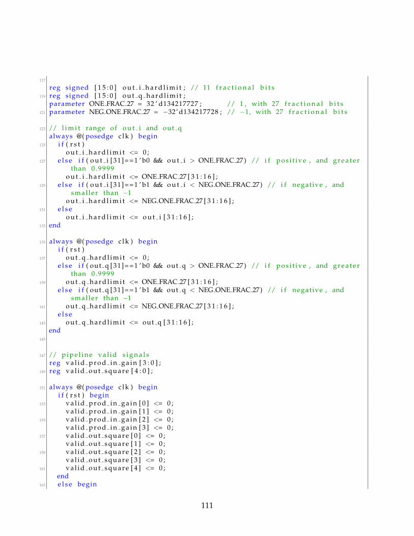
117
reg signed [ 1 5 : 0 ] o u t i h a r d l i m i t ; // 11 f r a c t i o n a l b i t s119 reg signed [ 1 5 : 0 ] o u t q h a r d l i m i t ;
parameter ONE FRAC 27 = 32 ’ d134217727 ; // 1 , with 27 f r a c t i o n a l b i t s121 parameter NEG ONE FRAC 27 = −32’ d134217728 ; // −1, with 27 f r a c t i o n a l b i t s
123 // l i m i t range of o u t i and out qalways @( posedge c l k ) begin
125 i f ( r s t )o u t i h a r d l i m i t <= 0 ;
127 e l s e i f ( o u t i [31]==1 ’ b0 && o u t i > ONE FRAC 27 ) // i f p o s i t i v e , and g r e a t e rthan 0 .9999
o u t i h a r d l i m i t <= ONE FRAC 27 [ 3 1 : 1 6 ] ;129 e l s e i f ( o u t i [31]==1 ’ b1 && o u t i < NEG ONE FRAC 27) // i f negative , and
smal ler than −1o u t i h a r d l i m i t <= NEG ONE FRAC 27 [ 3 1 : 1 6 ] ;
131 e l s eo u t i h a r d l i m i t <= o u t i [ 3 1 : 1 6 ] ;
133 end
135 always @( posedge c l k ) begini f ( r s t )
137 o u t q h a r d l i m i t <= 0 ;e l s e i f ( out q [31]==1 ’ b0 && out q > ONE FRAC 27 ) // i f p o s i t i v e , and g r e a t e r
than 0 .9999139 o u t q h a r d l i m i t <= ONE FRAC 27 [ 3 1 : 1 6 ] ;
e l s e i f ( out q [31]==1 ’ b1 && out q < NEG ONE FRAC 27) // i f negative , andsmal ler than −1
141 o u t q h a r d l i m i t <= NEG ONE FRAC 27 [ 3 1 : 1 6 ] ;e l s e
143 o u t q h a r d l i m i t <= out q [ 3 1 : 1 6 ] ;end
145
147 // p i p e l i n e va l id s i g n a l sreg v a l i d p r o d i n g a i n [ 3 : 0 ] ;
149 reg v a l i d o u t s q u a r e [ 4 : 0 ] ;
151 always @( posedge c l k ) begini f ( r s t ) begin
153 v a l i d p r o d i n g a i n [ 0 ] <= 0 ;v a l i d p r o d i n g a i n [ 1 ] <= 0 ;
155 v a l i d p r o d i n g a i n [ 2 ] <= 0 ;v a l i d p r o d i n g a i n [ 3 ] <= 0 ;
157 v a l i d o u t s q u a r e [ 0 ] <= 0 ;v a l i d o u t s q u a r e [ 1 ] <= 0 ;
159 v a l i d o u t s q u a r e [ 2 ] <= 0 ;v a l i d o u t s q u a r e [ 3 ] <= 0 ;
161 v a l i d o u t s q u a r e [ 4 ] <= 0 ;end
163 e l s e begin
111
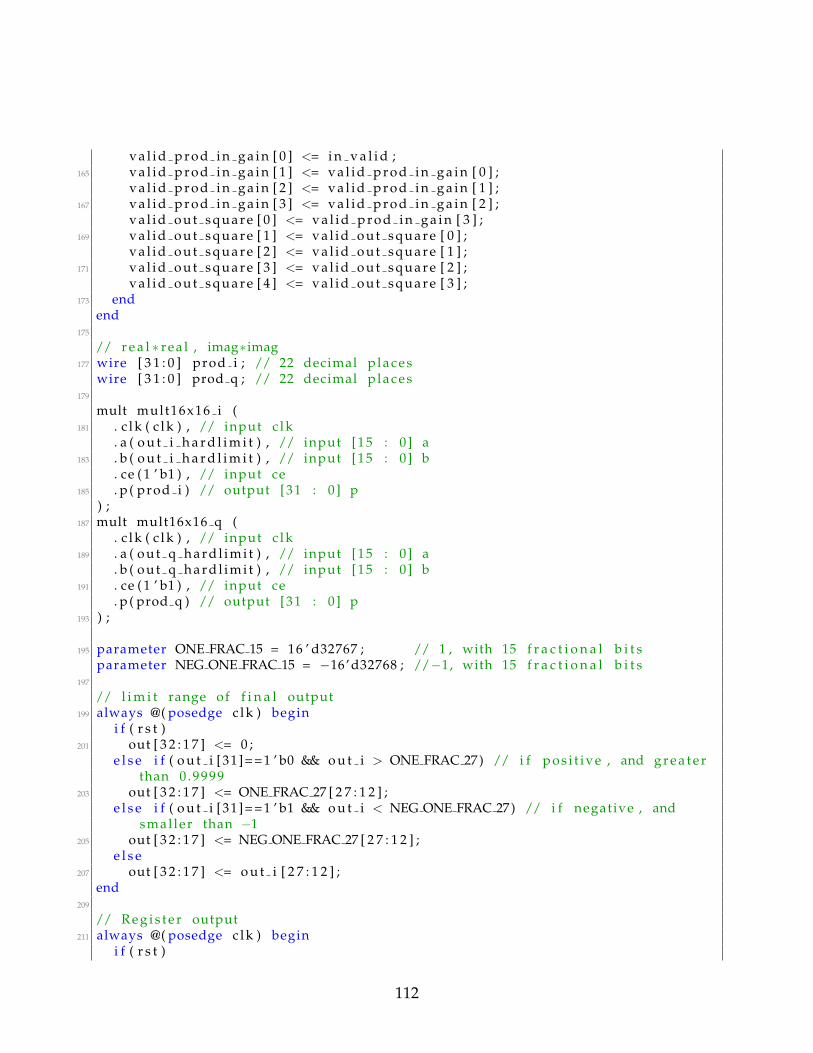
v a l i d p r o d i n g a i n [ 0 ] <= i n v a l i d ;165 v a l i d p r o d i n g a i n [ 1 ] <= v a l i d p r o d i n g a i n [ 0 ] ;
v a l i d p r o d i n g a i n [ 2 ] <= v a l i d p r o d i n g a i n [ 1 ] ;167 v a l i d p r o d i n g a i n [ 3 ] <= v a l i d p r o d i n g a i n [ 2 ] ;
v a l i d o u t s q u a r e [ 0 ] <= v a l i d p r o d i n g a i n [ 3 ] ;169 v a l i d o u t s q u a r e [ 1 ] <= v a l i d o u t s q u a r e [ 0 ] ;
v a l i d o u t s q u a r e [ 2 ] <= v a l i d o u t s q u a r e [ 1 ] ;171 v a l i d o u t s q u a r e [ 3 ] <= v a l i d o u t s q u a r e [ 2 ] ;
v a l i d o u t s q u a r e [ 4 ] <= v a l i d o u t s q u a r e [ 3 ] ;173 end
end175
// r e a l ∗ rea l , imag∗imag177 wire [ 3 1 : 0 ] prod i ; // 22 decimal p laces
wire [ 3 1 : 0 ] prod q ; // 22 decimal p laces179
mult mult16x16 i (181 . c l k ( c l k ) , // input c l k
. a ( o u t i h a r d l i m i t ) , // input [15 : 0 ] a183 . b ( o u t i h a r d l i m i t ) , // input [15 : 0 ] b
. ce ( 1 ’ b1 ) , // input ce185 . p ( prod i ) // output [31 : 0 ] p
) ;187 mult mult16x16 q (
. c l k ( c l k ) , // input c l k189 . a ( o u t q h a r d l i m i t ) , // input [15 : 0 ] a
. b ( o u t q h a r d l i m i t ) , // input [15 : 0 ] b191 . ce ( 1 ’ b1 ) , // input ce
. p ( prod q ) // output [31 : 0 ] p193 ) ;
195 parameter ONE FRAC 15 = 16 ’ d32767 ; // 1 , with 15 f r a c t i o n a l b i t sparameter NEG ONE FRAC 15 = −16’d32768 ; //−1, with 15 f r a c t i o n a l b i t s
197
// l i m i t range of f i n a l output199 always @( posedge c l k ) begin
i f ( r s t )201 out [ 3 2 : 1 7 ] <= 0 ;
e l s e i f ( o u t i [31]==1 ’ b0 && o u t i > ONE FRAC 27 ) // i f p o s i t i v e , and g r e a t e rthan 0 .9999
203 out [ 3 2 : 1 7 ] <= ONE FRAC 27 [ 2 7 : 1 2 ] ;e l s e i f ( o u t i [31]==1 ’ b1 && o u t i < NEG ONE FRAC 27) // i f negative , and
smal ler than −1205 out [ 3 2 : 1 7 ] <= NEG ONE FRAC 27 [ 2 7 : 1 2 ] ;
e l s e207 out [ 3 2 : 1 7 ] <= o u t i [ 2 7 : 1 2 ] ;
end209
// R e g i s t e r output211 always @( posedge c l k ) begin
i f ( r s t )
112
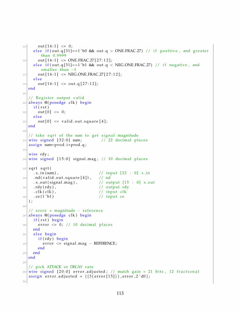
213 out [ 1 6 : 1 ] <= 0 ;e l s e i f ( out q [31]==1 ’ b0 && out q > ONE FRAC 27 ) // i f p o s i t i v e , and g r e a t e r
than 0 .9999215 out [ 1 6 : 1 ] <= ONE FRAC 27 [ 2 7 : 1 2 ] ;
e l s e i f ( out q [31]==1 ’ b1 && out q < NEG ONE FRAC 27) // i f negative , andsmal ler than −1
217 out [ 1 6 : 1 ] <= NEG ONE FRAC 27 [ 2 7 : 1 2 ] ;e l s e
219 out [ 1 6 : 1 ] <= out q [ 2 7 : 1 2 ] ;end
221
// R e g i s t e r output va l id223 always @( posedge c l k ) begin
i f ( r s t )225 out [ 0 ] <= 0 ;
e l s e227 out [ 0 ] <= v a l i d o u t s q u a r e [ 4 ] ;
end229
// take s q r t of the sum to get s i g n a l magnitude231 wire signed [ 3 2 : 0 ] sum ; // 22 decimal p laces
ass ign sum=prod i+prod q ;233
wire rdy ;235 wire signed [ 1 5 : 0 ] signal mag ; // 10 decimal p laces
237 s q r t s q r t (. x i n (sum) , // input [32 : 0 ] x i n
239 . nd ( v a l i d o u t s q u a r e [ 4 ] ) , // nd. x out ( signal mag ) , // output [15 : 0 ] x out
241 . rdy ( rdy ) , // output rdy. c l k ( c l k ) , // input c l k
243 . ce ( 1 ’ b1 ) // input ce) ;
245
// e r r o r = magnitude − r e f e r e n c e247 always @( posedge c l k ) begin
i f ( r s t ) begin249 e r r o r <= 0 ; // 10 decimal p laces
end251 e l s e begin
i f ( rdy ) begin253 e r r o r <= signal mag − REFERENCE ;
end255 end
end257
// pick ATTACK or DECAY r a t e259 wire signed [ 2 0 : 0 ] e r r o r a d j u s t e d ; // match gain = 21 b i t s , 12 f r a c t i o n a l
ass ign e r r o r a d j u s t e d = {{3{ e r r o r [ 1 5 ]}} , error , 2 ’ d0 } ;261
113
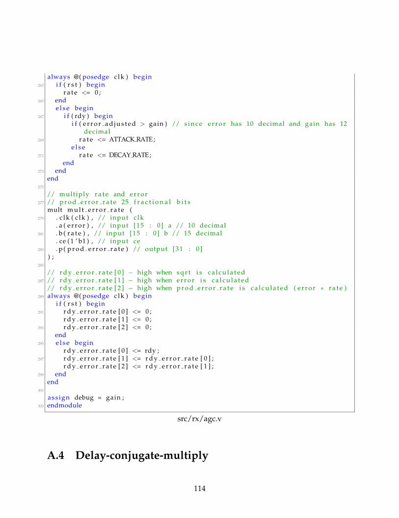
always @( posedge c l k ) begin263 i f ( r s t ) begin
r a t e <= 0 ;265 end
e l s e begin267 i f ( rdy ) begin
i f ( e r r o r a d j u s t e d > gain ) // s i n c e e r r o r has 10 decimal and gain has 12decimal
269 r a t e <= ATTACK RATE;e l s e
271 r a t e <= DECAY RATE;end
273 endend
275
// mult iply r a t e and e r r o r277 // p r o d e r r o r r a t e 25 f r a c t i o n a l b i t s
mult m u l t e r r o r r a t e (279 . c l k ( c l k ) , // input c l k
. a ( e r r o r ) , // input [15 : 0 ] a // 10 decimal281 . b ( r a t e ) , // input [15 : 0 ] b // 15 decimal
. ce ( 1 ’ b1 ) , // input ce283 . p ( p r o d e r r o r r a t e ) // output [31 : 0 ]
) ;285
// r d y e r r o r r a t e [ 0 ] − high when s q r t i s c a l c u l a t e d287 // r d y e r r o r r a t e [ 1 ] − high when e r r o r i s c a l c u l a t e d
// r d y e r r o r r a t e [ 2 ] − high when p r o d e r r o r r a t e i s c a l c u l a t e d ( e r r o r ∗ r a t e )289 always @( posedge c l k ) begin
i f ( r s t ) begin291 r d y e r r o r r a t e [ 0 ] <= 0 ;
r d y e r r o r r a t e [ 1 ] <= 0 ;293 r d y e r r o r r a t e [ 2 ] <= 0 ;
end295 e l s e begin
r d y e r r o r r a t e [ 0 ] <= rdy ;297 r d y e r r o r r a t e [ 1 ] <= r d y e r r o r r a t e [ 0 ] ;
r d y e r r o r r a t e [ 2 ] <= r d y e r r o r r a t e [ 1 ] ;299 end
end301
ass ign debug = gain ;303 endmodule
src/rx/agc.v
A.4 Delay-conjugate-multiply
114
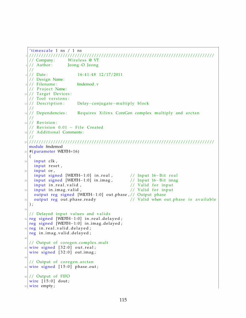
‘ t i m e s c a l e 1 ns / 1 ns2 /////////////////////////////////////////////////////////////////////////////
// Company : Wireless @ VT4 // Author : Jeong−O Jeong
//6 // Date : 1 6 : 4 1 : 4 8 12/17/2011
// Design Name:8 // Filename : fmdemod . v
// P r o j e c t Name:10 // Target Devices :
// Tool vers ions :12 // Descr ipt ion : Delay−conjugate−mult iply block
//14 // Dependencies : Requires X i l i n x CoreGen complex mult iply and arc tan
//16 // Revision :
// Revision 0 . 0 1 − F i l e Created18 // Addit ional Comments :
//20 /////////////////////////////////////////////////////////////////////////////
module fmdemod22 #( parameter WIDTH=16)
(24 input clk ,
input r e s e t ,26 input ce ,
input signed [WIDTH−1:0] i n r e a l , // Input 16−B i t r e a l28 input signed [WIDTH−1:0] in imag , // Input 16−B i t imag
input i n r e a l v a l i d , // Valid f o r input30 input in imag val id , // Valid f o r input
output reg signed [WIDTH−1:0] out phase , // Output phase32 output reg out phase ready // Valid when out phase i s a v a i l a b l e
) ;34
// Delayed input values and v a l i d s36 reg signed [WIDTH−1:0] i n r e a l d e l a y e d ;
reg signed [WIDTH−1:0] in imag delayed ;38 reg i n r e a l v a l i d d e l a y e d ;
reg in imag val id delayed ;40
// Output of coregen complex mult42 wire signed [ 3 2 : 0 ] o u t r e a l ;
wire signed [ 3 2 : 0 ] out imag ;44
// Output of coregen arc tan46 wire signed [ 1 5 : 0 ] phase out ;
48 // Output of FIFOwire [ 1 5 : 0 ] dout ;
50 wire empty ;
115
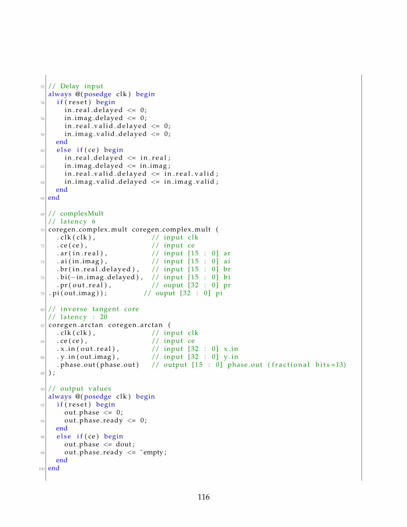
52 // Delay inputalways @( posedge c l k ) begin
54 i f ( r e s e t ) begini n r e a l d e l a y e d <= 0 ;
56 in imag delayed <= 0 ;i n r e a l v a l i d d e l a y e d <= 0 ;
58 in imag val id delayed <= 0 ;end
60 e l s e i f ( ce ) begini n r e a l d e l a y e d <= i n r e a l ;
62 in imag delayed <= in imag ;i n r e a l v a l i d d e l a y e d <= i n r e a l v a l i d ;
64 in imag val id delayed <= in imag val id ;end
66 end
68 // complexMult// l a t e n c y 6
70 coregen complex mult coregen complex mult (. c l k ( c l k ) , // input c l k
72 . ce ( ce ) , // input ce. ar ( i n r e a l ) , // input [15 : 0 ] ar
74 . a i ( in imag ) , // input [15 : 0 ] a i. br ( i n r e a l d e l a y e d ) , // input [15 : 0 ] br
76 . b i (− in imag delayed ) , // input [15 : 0 ] b i. pr ( o u t r e a l ) , // ouput [32 : 0 ] pr
78 . pi ( out imag ) ) ; // ouput [32 : 0 ] pi
80 // inverse tangent core// l a t e n c y : 20
82 coregen arc tan coregen arc tan (. c l k ( c l k ) , // input c l k
84 . ce ( ce ) , // input ce. x i n ( o u t r e a l ) , // input [32 : 0 ] x i n
86 . y in ( out imag ) , // input [32 : 0 ] y in. phase out ( phase out ) // output [15 : 0 ] phase out ( f r a c t i o n a l b i t s =13)
88 ) ;
90 // output valuesalways @( posedge c l k ) begin
92 i f ( r e s e t ) beginout phase <= 0 ;
94 out phase ready <= 0 ;end
96 e l s e i f ( ce ) beginout phase <= dout ;
98 out phase ready <= ˜ empty ;end
100 end
116
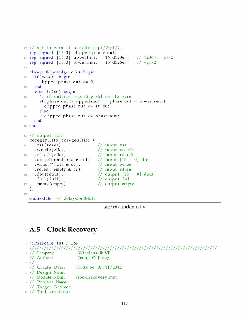
102 // s e t to zero i f outs ide [−pi /2: pi /2]reg signed [ 1 5 : 0 ] c l ipped phase out ;
104 reg signed [ 1 5 : 0 ] upperl imit = 16 ’ d12868 ; // 12868 = pi /2reg signed [ 1 5 : 0 ] lower l imi t = 16 ’ d52668 ; // −pi /2
106
always @( posedge c l k ) begin108 i f ( r e s e t ) begin
c l ipped phase out <= 0 ;110 end
e l s e i f ( ce ) begin112 // i f outs ide [−pi /2: pi /2] s e t to zero
i f ( phase out > upperl imit | | phase out < lower l imi t )114 c l ipped phase out <= 16 ’ d0 ;
e l s e116 c l ipped phase out <= phase out ;
end118 end
120 // output f i f oc o r e g e n f i f o c o r e g e n f i f o (
122 . r s t ( r e s e t ) , // input r s t. wr clk ( c l k ) , // input wr clk
124 . r d c l k ( c l k ) , // input r d c l k. din ( c l ipped phase out ) , // input [15 : 0 ] din
126 . wr en ( ˜ f u l l & ce ) , // input wr en. rd en ( ˜ empty & ce ) , // input rd en
128 . dout ( dout ) , // output [15 : 0 ] dout. f u l l ( f u l l ) , // output f u l l
130 . empty ( empty ) // output empty) ;
132
endmodule // delayConjMult
src/rx/fmdemod.v
A.5 Clock Recovery
1 ‘ t i m e s c a l e 1ns / 1ps/////////////////////////////////////////////////////////////////////////////
3 // Company : Wireless @ VT// Author : Jeong−O Jeong
5 //// Create Date : 1 1 : 3 3 : 5 6 07/11/2012
7 // Design Name:// Module Name: clock recovery mm
9 // P r o j e c t Name:// Target Devices :
11 // Tool vers ions :
117
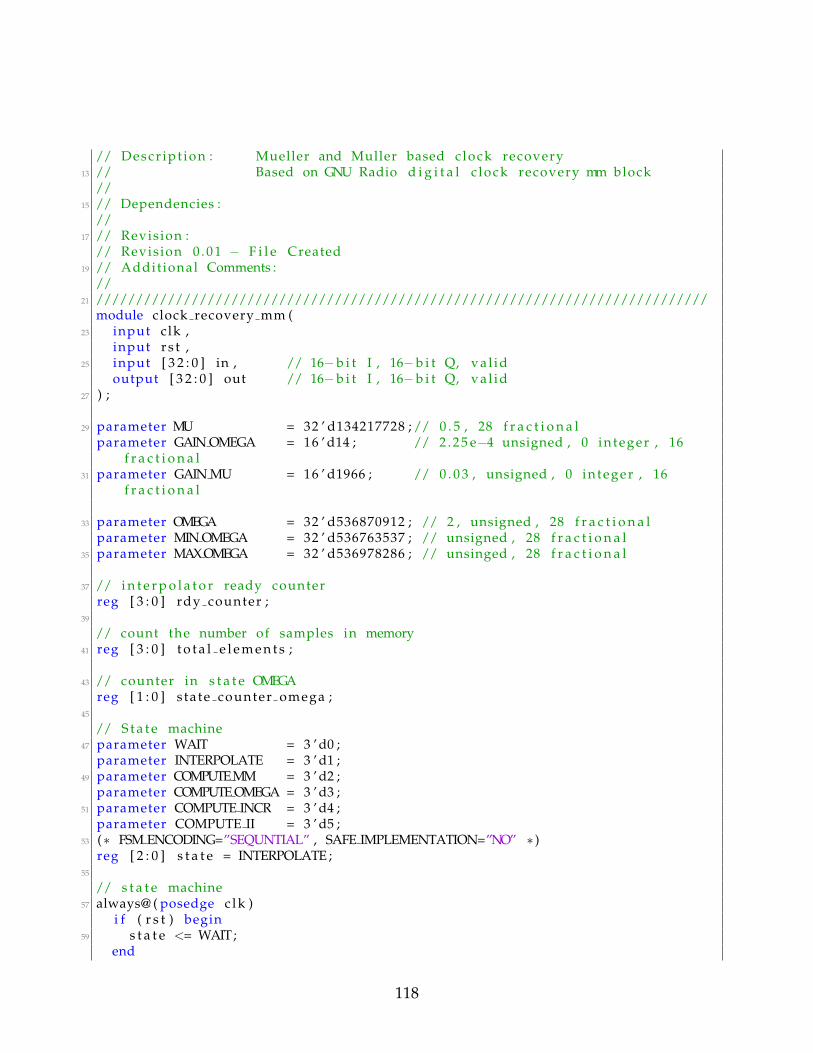
// Descr ipt ion : Mueller and Muller based c lock recovery13 // Based on GNU Radio d i g i t a l c lock recovery mm block
//15 // Dependencies :
//17 // Revision :
// Revision 0 . 0 1 − F i l e Created19 // Addit ional Comments :
//21 /////////////////////////////////////////////////////////////////////////////
module clock recovery mm (23 input clk ,
input r s t ,25 input [ 3 2 : 0 ] in , // 16−b i t I , 16−b i t Q, va l id
output [ 3 2 : 0 ] out // 16−b i t I , 16−b i t Q, va l id27 ) ;
29 parameter MU = 32 ’ d134217728 ; // 0 . 5 , 28 f r a c t i o n a lparameter GAIN OMEGA = 16 ’ d14 ; // 2 . 2 5 e−4 unsigned , 0 in teger , 16
f r a c t i o n a l31 parameter GAIN MU = 16 ’ d1966 ; // 0 . 0 3 , unsigned , 0 in teger , 16
f r a c t i o n a l
33 parameter OMEGA = 32 ’ d536870912 ; // 2 , unsigned , 28 f r a c t i o n a lparameter MIN OMEGA = 32 ’ d536763537 ; // unsigned , 28 f r a c t i o n a l
35 parameter MAXOMEGA = 32 ’ d536978286 ; // unsinged , 28 f r a c t i o n a l
37 // i n t e r p o l a t o r ready counterreg [ 3 : 0 ] rdy counter ;
39
// count the number of samples in memory41 reg [ 3 : 0 ] t o t a l e l e m e n t s ;
43 // counter in s t a t e OMEGAreg [ 1 : 0 ] s ta te counter omega ;
45
// S t a t e machine47 parameter WAIT = 3 ’ d0 ;
parameter INTERPOLATE = 3 ’ d1 ;49 parameter COMPUTEMM = 3 ’ d2 ;
parameter COMPUTE OMEGA = 3 ’ d3 ;51 parameter COMPUTE INCR = 3 ’ d4 ;
parameter COMPUTE II = 3 ’ d5 ;53 (∗ FSM ENCODING=”SEQUNTIAL” , SAFE IMPLEMENTATION=”NO” ∗ )
reg [ 2 : 0 ] s t a t e = INTERPOLATE ;55
// s t a t e machine57 always@ ( posedge c l k )
i f ( r s t ) begin59 s t a t e <= WAIT;
end
118

61 e l s e begincase ( s t a t e )
63 WAIT : begini f ( t o t a l e l e m e n t s > 10)
65 s t a t e <= INTERPOLATE ;e l s e
67 s t a t e <= WAIT;end
69 INTERPOLATE : begini f ( rdy counter == 7) // i n t e r p o l a t i o n i s f i n i s h e d with 8 input samples
;71 // 7 , because rdy counter changes to 8 one c lock c y c l e a f t e r the 8 th
output i s computeds t a t e <= COMPUTEMM;
73 e l s es t a t e <= INTERPOLATE ;
75 endCOMPUTEMM : begin
77 i f ( 1 ’ b1 )s t a t e <= COMPUTE OMEGA;
79 e l s es t a t e <= COMPUTEMM;
81 endCOMPUTE OMEGA : begin
83 i f ( s ta te counter omega == 1)s t a t e <= COMPUTE INCR;
85 e l s es t a t e <= COMPUTE OMEGA;
87 endCOMPUTE INCR : begin
89 i f ( 1 ’ b1 )s t a t e <= COMPUTE II ;
91 e l s es t a t e <= COMPUTE INCR;
93 endCOMPUTE II : begin
95 i f ( 1 ’ b1 )s t a t e <= WAIT;
97 e l s es t a t e <= COMPUTE II ;
99 endendcase
101 end
103 // input r e g i s t e r sreg signed [ 1 5 : 0 ] i r e g ;
105 reg va l id ;
107 // f r a c t i o n a l o f f s e treg signed [ 3 1 : 0 ] mu; // 28 f r a c t i o n a l
109 // samples per symbol
119
reg signed [ 3 1 : 0 ] omega ; // 28 f r a c t i o n a l111 // e r r o r
reg signed [ 1 5 : 0 ] mm val ; // signed 4 integer , 12 f r a c t i o n a l113
115 // I n t e r p o l a t o r wireswire rfd , rdy ;
117
// r e g i s t e r inputs ( only r e a l value needed )119 always @( posedge c l k ) begin
i f ( r s t ) begin121 i r e g <= 0 ;
end123 e l s e i f ( in [ 0 ] ) begin
i r e g <= in [ 3 2 : 1 7 ] ;125 end
val id <= in [ 0 ] ;127 end
129 // wires needed f o r 2 port block ramreg [ 3 : 0 ] addr write ;
131 reg [ 3 : 0 ] i i ; // pointer to s t a r t of read l o c a t i o nreg [ 3 : 0 ] addr read ; // a c t u a l memory read index
133 wire [ 1 5 : 0 ] dout mem ;reg valid mem ;
135
reg [ 3 1 : 0 ] i n c r ; // increment f o r read index , 28 f r a c t i o n a l b i t137
// t o t a l elements counter139 always @( posedge c l k ) begin
i f ( r s t ) begin141 t o t a l e l e m e n t s <= 0 ;
end143 e l s e i f ( va l id ) begin
t o t a l e l e m e n t s <= t o t a l e l e m e n t s + 1 ;145 end
i f ( s t a t e == COMPUTE II ) begin147 t o t a l e l e m e n t s <= t o t a l e l e m e n t s − i n c r [ 3 1 : 2 8 ] ;
end149 end
151 // write addressalways @( posedge c l k ) begin
153 i f ( r s t ) beginaddr write <= 1 ’ b0 ;
155 end// whenever there i s a new data increment wri te addr
157 e l s e i f ( va l id ) beginaddr write <= addr write + 1 ;
159 endend
120
161
// prepare f o r m u l t i p l i c a t i o n163 wire signed [ 3 1 : 0 ] gain mu ;
wire signed [ 3 1 : 0 ] gain omega ;165 wire signed [ 3 1 : 0 ] mm val ;
ass ign gain omega = {16 ’ b0 , GAIN OMEGA} ;167 ass ign gain mu = {16 ’ b0 , GAIN MU} ;
ass ign mm val = {{16{mm val [ 1 5 ]}} , mm val } ;169
reg signed [ 3 1 : 0 ] prod gainMu mmVal ; // 28 f r a c t i o n a l171 always @( posedge c l k ) begin
i f ( r s t ) begin173 prod gainMu mmVal <= 0 ;
end175 e l s e begin
// 16 f r a c t i o n a l ∗ 12 f r a c t i o n a l = 28 f r a c t i o n a l177 prod gainMu mmVal <= gain mu ∗ mm val ;
end179 end
181 // increment f o r read index , 28 f r a c t i o n a l b i talways @( posedge c l k ) begin
183 i f ( r s t ) begini n c r <= 0 ;
185 ende l s e i f ( s t a t e == COMPUTE INCR) begin
187 // 28 + 28 + 28 f r a c t i o n a li n c r <= mu + omega + prod gainMu mmVal ;
189 endend
191
wire [ 3 : 0 ] i n c r i n t ;193 ass ign i n c r i n t = i n c r [ 3 1 : 2 8 ] ;
195 // pointer to s t a r t indexalways @( posedge c l k ) begin
197 i f ( r s t ) begini i <= 0 ;
199 ende l s e i f ( s t a t e == COMPUTE II ) begin
201 i i <= i i + i n c r [ 3 1 : 2 8 ] ;end
203 end
205 // read addressalways @( posedge c l k ) begin
207 i f ( r s t ) beginaddr read <= 0 ;
209 ende l s e i f ( s t a t e == INTERPOLATE) begin
121
211 i f ( r fd && ˜ rdy ) // using ˜ rdy because i t goes high 8 c y c l e s l a t e r s i n c ef i r s t new data
addr read <= addr read + 1 ’ b1 ;213 end
e l s e // s e t to i i215 addr read <= i i ;
end217
// rdy counter219 always @( posedge c l k ) begin
i f ( r s t ) begin221 rdy counter <= 0 ;
end223 e l s e i f ( s t a t e == INTERPOLATE) begin
i f ( rdy )225 rdy counter <= rdy counter + 1 ;
end227 e l s e
rdy counter <= 0 ;229 end
231 core mem core mem (// port a
233 . c lka ( c l k ) , // input c lka. wea ( va l id ) , // input [0 : 0 ] wea
235 . ena ( ˜ r s t ) ,. addra ( addr write ) , // input [3 : 0 ] addra
237 . dina ( i r e g ) , // input [15 : 0 ] dina. douta ( ) , // output [15 : 0 ] douta
239 // port b. c lkb ( c l k ) , // input c lkb
241 . enb ( ˜ r s t ) ,. web( 1 ’ b0 ) , // input [0 : 0 ] web
243 . addrb ( addr read ) , // input [3 : 0 ] addrb. dinb ( 1 6 ’ b0 ) , // input [15 : 0 ] dinb
245 . doutb ( dout mem ) // output [15 : 0 ] doutb) ;
247
wire signed [ 3 1 : 0 ] dout ; // f r a c t i o n a l 30249 reg signed [ 1 5 : 0 ] outputs [ 0 : 1 ] ; // 14 f r a c t i o n a l b i t s
251 // s t o r e previous and current outputs of the i n t e r p o l a t o ralways @( posedge c l k ) begin
253 i f ( r s t ) beginoutputs [ 0 ] <= 0 ;
255 outputs [ 1 ] <= 0 ;end
257 e l s e i f ( rdy counter == 7) beginoutputs [ 0 ] <= dout [ 3 1 : 1 6 ] ; // 14 f r a c t i o n a l b i t s
259 outputs [ 1 ] <= outputs [ 0 ] ;end
122
261 end
263 //ass ign out = {dout [ 3 0 : 1 5 ] , 16 ’ b0 , rdy counter == 7} ;ass ign out = {dout [ 3 1 : 1 6 ] , 16 ’ b0 , rdy counter == 7} ;
265
wire signed [ 1 5 : 0 ] sample current ; // 14 f r a c t i o n a l b i t s267 wire signed [ 1 5 : 0 ] s a m p l e l a s t ;
ass ign sample current = outputs [ 0 ] ;269 ass ign s a m p l e l a s t =outputs [ 1 ] ;
271 // mm error , 12 f r a c t i o n a l b i t swire signed [ 1 5 : 0 ] mm val 0 , mm val 1 , mm val 2 , mm val 3 ;
273 ass ign mm val 0 = −sample current + s a m p l e l a s t ; // 14 f r a c t i o n a lass ign mm val 1 = sample current + s a m p l e l a s t ;
275 ass ign mm val 2 = −sample current − s a m p l e l a s t ;ass ign mm val 3 = sample current − s a m p l e l a s t ;
277
// compute a l l four cases and pick one279 always @( posedge c l k ) begin
i f ( r s t ) begin281 mm val <= 0 ;
end283 e l s e i f ( s t a t e == COMPUTEMM) begin
i f ( s a m p l e l a s t < 0 && sample current < 0)285 mm val <= {{2{mm val 0 [ 1 5 ]}} , mm val 0 [ 1 5 : 2 ] } ;
e l s e i f ( s a m p l e l a s t > 0 && sample current < 0)287 mm val <= {{2{mm val 1 [ 1 5 ]}} , mm val 1 [ 1 5 : 2 ] } ;
e l s e i f ( s a m p l e l a s t < 0 && sample current > 0)289 mm val <= {{2{mm val 2 [ 1 5 ]}} , mm val 2 [ 1 5 : 2 ] } ;
e l s e291 mm val <= {{2{mm val 3 [ 1 5 ]}} , mm val 3 [ 1 5 : 2 ] } ;
end293 end
295 // OMEGA s t a t e counteralways @( posedge c l k ) begin
297 i f ( r s t ) beginstate counter omega <= 0 ;
299 ende l s e i f ( s t a t e == COMPUTE OMEGA) begin
301 s tate counter omega <= state counter omega + 1 ’ b1 ;end
303 e l s es tate counter omega <= 0 ;
305 end
307 reg signed [ 3 1 : 0 ] prod gainOmega mmVal ; // 28 f r a c t i o n a l// GAIN OMEGA ∗ mm val
309 always @( posedge c l k ) begini f ( r s t ) begin
311 prod gainOmega mmVal <= 0 ;
123

end313 e l s e begin
// 16 f r a c t i o n a l ∗ 12 f r a c t i o n a l = 28 f r a c t i o n a l315 prod gainOmega mmVal <= gain omega ∗ mm val ;
end317 end
319 wire [ 3 2 : 0 ] omega preclip = omega + prod gainOmega mmVal ;
321 // omega = samples per symbol , 28 f r a c t i o n a lalways @( posedge c l k ) begin
323 i f ( r s t ) beginomega <= OMEGA;
325 ende l s e i f ( s t a t e == COMPUTE OMEGA & state counter omega == 1) begin
327 i f ( omega preclip > MAXOMEGA)omega <= MAXOMEGA;
329 e l s e i f ( omega preclip < MIN OMEGA)omega <= MIN OMEGA;
331 e l s eomega <= omega preclip ;
333 endend
335
// f r a c t i o n a l o f f s e t , 28 f r a c t i o n a l337 always @( posedge c l k ) begin
i f ( r s t ) begin339 mu <= MU;
end341 e l s e i f ( s t a t e == COMPUTE II ) begin
mu <= { i n c r [ 2 7 : 0 ] } ; // f r a c t i o n a l port ion of i n c r343 end
end345
wire [ 7 : 0 ] f i l t e r s e l ;347 wire signed [ 3 1 : 0 ] round mu ;
wire signed [ 3 1 : 0 ] h a l f ;349 ass ign h a l f = 1 ’ b1<<20;
ass ign round mu = mu + h a l f ;351 ass ign f i l t e r s e l = round mu [ 2 8 : 2 1 ] ;
353 // r e g s i t e r to i n d i c a t e i f the s t a t e i s i n t e r p o l a t ereg r e g s t a t e i n t e r p o l a t e ;
355 always @( posedge c l k ) begini f ( r s t )
357 r e g s t a t e i n t e r p o l a t e <= 0 ;e l s e
359 r e g s t a t e i n t e r p o l a t e <= ( s t a t e == INTERPOLATE) ;end
361
wire nd ;
124
363 ass ign nd = r e g s t a t e i n t e r p o l a t e & ˜ rdy & ( s t a t e == INTERPOLATE) ;
365 // 8−tap i n t e r p o l a t o rc o r e i n t e r p o l a t o r c o r e i n t e r p o l a t o r (
367 . s c l r ( ˜ r e g s t a t e i n t e r p o l a t e ) , // input s c l r. c l k ( c l k ) , // input c l k
369 . ce ( ˜ r s t ) , // input ce. nd ( nd ) , // input nd
371 . f i l t e r s e l ( f i l t e r s e l ) , // input [7 : 0 ] f i l t e r s e l. r fd ( r fd ) , // ouput r fd
373 . rdy ( rdy ) , // ouput rdy. din ( dout mem ) , // input [15 : 0 ] din
375 . dout ( dout ) ) ; // ouput [31 : 0 ] dout
377 endmodule
src/rx/clock recovery mm.v
A.6 Symbol Correlation
1 ‘ t i m e s c a l e 1ns / 1ps/////////////////////////////////////////////////////////////////////////////
3 // Company : Wireless @ VT// Engineer : Jeong−O Jeong
5 //// Create Date : 0 1 : 1 4 : 3 3 12/11/2011
7 // Design Name:// Module Name: f ir bank sym
9 // P r o j e c t Name:// Target Devices :
11 // Tool vers ions :// Descr ipt ion : Find the symbol c o r r e l a t i o n s of 16 symbols
13 //// Dependencies : CoreGen FIR and FIFO
15 //// Revision :
17 // Revision 0 . 0 1 − F i l e Created// Addit ional Comments :
19 ///////////////////////////////////////////////////////////////////////////////
21 module f ir bank sym#( parameter WIDTH=16 , parameter N=16)
23 (input clk ,
25 input r e s e t ,input s t r o b e i n , // 2Mhz s t rob e
27 input s t robe out , // 2MHz st rob einput [WIDTH−1:0] din , // input chip
125
29 output out r fd ,output [ 2 1 : 0 ] out 0 , // symbol c o r r e l a t i o n output 0
31 output [ 2 1 : 0 ] out 1 ,output [ 2 1 : 0 ] out 2 ,
33 output [ 2 1 : 0 ] out 3 ,output [ 2 1 : 0 ] out 4 ,
35 output [ 2 1 : 0 ] out 5 ,output [ 2 1 : 0 ] out 6 ,
37 output [ 2 1 : 0 ] out 7 ,output [ 2 1 : 0 ] out 8 ,
39 output [ 2 1 : 0 ] out 9 ,output [ 2 1 : 0 ] out 10 ,
41 output [ 2 1 : 0 ] out 11 ,output [ 2 1 : 0 ] out 12 ,
43 output [ 2 1 : 0 ] out 13 ,output [ 2 1 : 0 ] out 14 ,
45 output [ 2 1 : 0 ] out 15 // symbol c o r r e l a t i o n output 15) ;
47
genvar i ;49
wire rfd [ 0 : 1 5 ] ;51 wire rdy [ 0 : 1 5 ] ;
wire [ 2 1 : 0 ] dout [ 0 : 1 5 ] ;53 wire f i f o f u l l s y m [ 0 : 1 5 ] ;
wire fifo empty sym [ 0 : 1 5 ] ;55 wire [ 2 4 : 0 ] f i fo dout sym [ 0 : 1 5 ] ;
57 ass ign o u t r f d = rfd [ 0 ] ;
59
// output s i g n a l s61 ass ign out 0 = f i fo dout sym [ 0 ] [ 2 1 : 0 ] ;
ass ign out 1 = f i fo dout sym [ 1 ] [ 2 1 : 0 ] ;63 ass ign out 2 = f i fo dout sym [ 2 ] [ 2 1 : 0 ] ;
ass ign out 3 = f i fo dout sym [ 3 ] [ 2 1 : 0 ] ;65 ass ign out 4 = f i fo dout sym [ 4 ] [ 2 1 : 0 ] ;
ass ign out 5 = f i fo dout sym [ 5 ] [ 2 1 : 0 ] ;67 ass ign out 6 = f i fo dout sym [ 6 ] [ 2 1 : 0 ] ;
ass ign out 7 = f i fo dout sym [ 7 ] [ 2 1 : 0 ] ;69 ass ign out 8 = f i fo dout sym [ 8 ] [ 2 1 : 0 ] ;
ass ign out 9 = f i fo dout sym [ 9 ] [ 2 1 : 0 ] ;71 ass ign out 10 = f i fo dout sym [ 1 0 ] [ 2 1 : 0 ] ;
ass ign out 11 = f i fo dout sym [ 1 1 ] [ 2 1 : 0 ] ;73 ass ign out 12 = f i fo dout sym [ 1 2 ] [ 2 1 : 0 ] ;
ass ign out 13 = f i fo dout sym [ 1 3 ] [ 2 1 : 0 ] ;75 ass ign out 14 = f i fo dout sym [ 1 4 ] [ 2 1 : 0 ] ;
ass ign out 15 = f i fo dout sym [ 1 5 ] [ 2 1 : 0 ] ;77
// generate 16 c o r r e l a t i o n FIR f i l t e r s79 generate
126
f o r ( i =0 ; i<N; i = i +1) begin : coregen f i r sym81 co re gen f i r sy m 0 coregen f i r sym (
. c l k ( c l k ) , // input c l k83 . f i l t e r s e l ( i ) , // input [3 : 0 ] f i l t e r s e l
. r fd ( r fd [ i ] ) , // ouput r fd85 . rdy ( rdy [ i ] ) , // ouput rdy
. din ( din ) , // input [15 : 0 ] din87 . dout ( dout [ i ] ) ) ; // ouput [21 : 0 ] dout
end89 endgenerate
91 // generate 16 FIFO ’ sgenerate
93 f o r ( i =0 ; i<N; i = i +1) begin : f i fo symc o r e g e n f i f o 5 1 2 2 5 coregen f i fo 25 sym (
95 . c l k ( c l k ) , // input c l k. r s t ( r e s e t ) , // input r s t
97 . din ({{3{dout [ i ] [ 2 1 ] } } , dout [ i ] } ) , // input [24 : 0 ] din. wr en ( ˜ f i f o f u l l s y m [ i ] & rdy [ i ] ) , // input wr en
99 . rd en ( ˜ f ifo empty sym [ i ] & s t r o b e o u t ) , // input rd en. dout ( f i fo dout sym [ i ] ) , // output [24 : 0 ] dout
101 . f u l l ( f i f o f u l l s y m [ i ] ) , // output f u l l. empty ( fifo empty sym [ i ] ) // output empty
103 ) ;end
105 endgenerate
107 endmodule
src/rx/fir bank sym.v
A.7 Find Max 16-input
1 /////////////////////////////////////////////////////////////////////////////// Company : Wireless @ VT
3 // Author : Jeong−O Jeong//
5 // Date : 1 6 : 3 9 : 4 8 12/17/2011// Design Name:
7 // Filename : findmax . v// P r o j e c t Name:
9 // Target Devices :// Tool vers ions :
11 // Descr ipt ion : f ind maximum between two values//
13 // Dependencies ://
15 // Revision :
127

// Revision 0 . 0 1 − F i l e Created17 // Addit ional Comments :
//19 /////////////////////////////////////////////////////////////////////////////
‘ t i m e s c a l e 1 ns / 1 ns21
module findmax23 #( parameter WIDTH=22)
(25 clk ,
ce ,27 r e s e t ,
index1 , // index of f i r s t element29 value1 , // value of f i r s t element
index2 , // index of second element31 value2 , // value of second element
index out , // index of max element33 value out // value of max element
) ;35
input c l k ;37 input ce ;
input r e s e t ;39 input [ 1 5 : 0 ] index1 ; // uf ix16
input [ 1 5 : 0 ] index2 ; // uf ix1641 input signed [WIDTH−1:0] value1 ; // s f ix16 En14
input signed [WIDTH−1:0] value2 ; // s f ix16 En1443
output reg [ 1 5 : 0 ] index out ; // uf ix1645 output reg [WIDTH−1:0] value out ; // s f ix16 En14
47 // output the index of max elementalways @( posedge c l k )
49 begini f ( r e s e t ) begin
51 index out = 0 ;end
53 e l s e begini f ( ce )
55 index out = ( value1 > value2 ) ? index1 : index2 ;end
57 end
59 // output the value of max elementalways @( posedge c l k )
61 begini f ( r e s e t )
63 value out = 0 ;e l s e
65 i f ( ce )value out = ( value1 > value2 ) ? value1 : value2 ;
128
67 end
69 endmodule // findmax
src/rx/findmax.v
A.8 Find Max 2-input
‘ t i m e s c a l e 1 ns / 1 ns2 /////////////////////////////////////////////////////////////////////////////
// Company : Wireless @ VT4 // Author : Jeong−O Jeong
//6 // Date : 1 6 : 3 9 : 5 9 12/17/2011
// Design Name:8 // Filename : findmax16 . v
// P r o j e c t Name:10 // Target Devices :
// Tool vers ions :12 // Descr ipt ion : f ind the maximum among 16 d i f f e r e n t values
//14 // Dependencies :
//16 // Revision :
// Revision 0 . 0 1 − F i l e Created18 // Addit ional Comments :
//20 /////////////////////////////////////////////////////////////////////////////
module findmax1622 #( parameter WIDTH=22)
(24 input clk ,
input ce ,26 input r e s e t ,
input [WIDTH−1:0] value0 ,28 input [WIDTH−1:0] value1 ,
input [WIDTH−1:0] value2 ,30 input [WIDTH−1:0] value3 ,
input [WIDTH−1:0] value4 ,32 input [WIDTH−1:0] value5 ,
input [WIDTH−1:0] value6 ,34 input [WIDTH−1:0] value7 ,
input [WIDTH−1:0] value8 ,36 input [WIDTH−1:0] value9 ,
input [WIDTH−1:0] value10 ,38 input [WIDTH−1:0] value11 ,
input [WIDTH−1:0] value12 ,40 input [WIDTH−1:0] value13 ,
129

input [WIDTH−1:0] value14 ,42 input [WIDTH−1:0] value15 ,
output [ 1 5 : 0 ] index out ,44 output signed [WIDTH−1:0] value out ,
output reg [WIDTH−1:0] passthrough46 ) ;
48 // max index of 8 values when comparing 16 valueswire [ 1 5 : 0 ] index 1 1 ;
50 wire [ 1 5 : 0 ] index 1 2 ;wire [ 1 5 : 0 ] index 1 3 ;
52 wire [ 1 5 : 0 ] index 1 4 ;wire [ 1 5 : 0 ] index 1 5 ;
54 wire [ 1 5 : 0 ] index 1 6 ;wire [ 1 5 : 0 ] index 1 7 ;
56 wire [ 1 5 : 0 ] index 1 8 ;
58 // max index of 4 values when comparing 8 valueswire [ 1 5 : 0 ] index 2 1 ;
60 wire [ 1 5 : 0 ] index 2 2 ;wire [ 1 5 : 0 ] index 2 3 ;
62 wire [ 1 5 : 0 ] index 2 4 ;
64 // max index of 2 values when comparing 4 valueswire [ 1 5 : 0 ] index 3 1 ;
66 wire [ 1 5 : 0 ] index 3 2 ;
68 // max 8 values when comparing 16 valueswire signed [WIDTH−1:0] va lue 1 1 ;
70 wire signed [WIDTH−1:0] va lue 1 2 ;wire signed [WIDTH−1:0] va lue 1 3 ;
72 wire signed [WIDTH−1:0] va lue 1 4 ;wire signed [WIDTH−1:0] va lue 1 5 ;
74 wire signed [WIDTH−1:0] va lue 1 6 ;wire signed [WIDTH−1:0] va lue 1 7 ;
76 wire signed [WIDTH−1:0] va lue 1 8 ;
78 // max 4 values when comparing 8 valueswire signed [WIDTH−1:0] va lue 2 1 ;
80 wire signed [WIDTH−1:0] va lue 2 2 ;wire signed [WIDTH−1:0] va lue 2 3 ;
82 wire signed [WIDTH−1:0] va lue 2 4 ;
84 // max 2 values when comparing 4 valueswire signed [WIDTH−1:0] va lue 3 1 ;
86 wire signed [WIDTH−1:0] va lue 3 2 ;
88 // 1 s t s tage// value0 , value1
90 findmax findmax1 ( clk , ce , r e s e t , 16 ’ d0 , value0 , 16 ’ d1 , value1 , index 1 1 ,va lue 1 1 ) ;
130
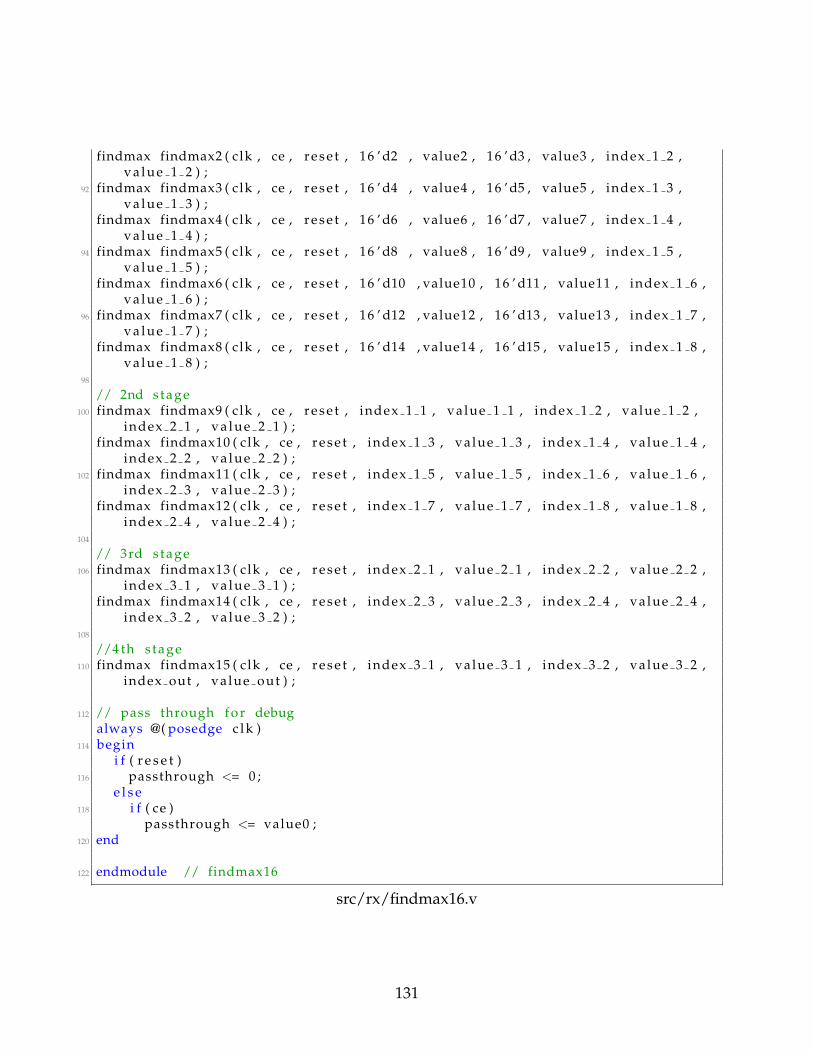
findmax findmax2 ( clk , ce , r e s e t , 16 ’ d2 , value2 , 16 ’ d3 , value3 , index 1 2 ,va lue 1 2 ) ;
92 findmax findmax3 ( clk , ce , r e s e t , 16 ’ d4 , value4 , 16 ’ d5 , value5 , index 1 3 ,va lue 1 3 ) ;
findmax findmax4 ( clk , ce , r e s e t , 16 ’ d6 , value6 , 16 ’ d7 , value7 , index 1 4 ,va lue 1 4 ) ;
94 findmax findmax5 ( clk , ce , r e s e t , 16 ’ d8 , value8 , 16 ’ d9 , value9 , index 1 5 ,va lue 1 5 ) ;
findmax findmax6 ( clk , ce , r e s e t , 16 ’ d10 , value10 , 16 ’ d11 , value11 , index 1 6 ,va lue 1 6 ) ;
96 findmax findmax7 ( clk , ce , r e s e t , 16 ’ d12 , value12 , 16 ’ d13 , value13 , index 1 7 ,va lue 1 7 ) ;
findmax findmax8 ( clk , ce , r e s e t , 16 ’ d14 , value14 , 16 ’ d15 , value15 , index 1 8 ,va lue 1 8 ) ;
98
// 2nd stage100 findmax findmax9 ( clk , ce , r e s e t , index 1 1 , value 1 1 , index 1 2 , value 1 2 ,
index 2 1 , va lue 2 1 ) ;findmax findmax10 ( clk , ce , r e s e t , index 1 3 , value 1 3 , index 1 4 , value 1 4 ,
index 2 2 , va lue 2 2 ) ;102 findmax findmax11 ( clk , ce , r e s e t , index 1 5 , value 1 5 , index 1 6 , value 1 6 ,
index 2 3 , va lue 2 3 ) ;findmax findmax12 ( clk , ce , r e s e t , index 1 7 , value 1 7 , index 1 8 , value 1 8 ,
index 2 4 , va lue 2 4 ) ;104
// 3rd stage106 findmax findmax13 ( clk , ce , r e s e t , index 2 1 , value 2 1 , index 2 2 , value 2 2 ,
index 3 1 , va lue 3 1 ) ;findmax findmax14 ( clk , ce , r e s e t , index 2 3 , value 2 3 , index 2 4 , value 2 4 ,
index 3 2 , va lue 3 2 ) ;108
//4 th stage110 findmax findmax15 ( clk , ce , r e s e t , index 3 1 , value 3 1 , index 3 2 , value 3 2 ,
index out , value out ) ;
112 // pass through f o r debugalways @( posedge c l k )
114 begini f ( r e s e t )
116 passthrough <= 0 ;e l s e
118 i f ( ce )passthrough <= value0 ;
120 end
122 endmodule // findmax16
src/rx/findmax16.v
131
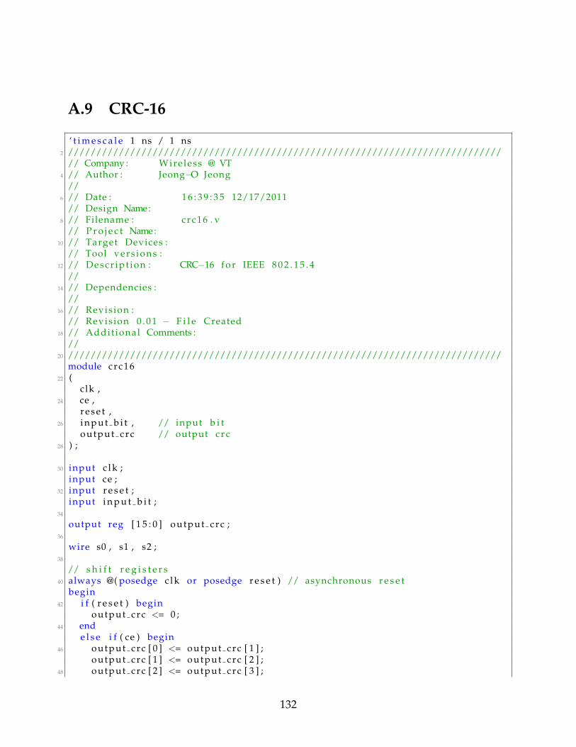
A.9 CRC-16
‘ t i m e s c a l e 1 ns / 1 ns2 /////////////////////////////////////////////////////////////////////////////
// Company : Wireless @ VT4 // Author : Jeong−O Jeong
//6 // Date : 1 6 : 3 9 : 3 5 12/17/2011
// Design Name:8 // Filename : crc16 . v
// P r o j e c t Name:10 // Target Devices :
// Tool vers ions :12 // Descr ipt ion : CRC−16 f o r IEEE 8 0 2 . 1 5 . 4
//14 // Dependencies :
//16 // Revision :
// Revision 0 . 0 1 − F i l e Created18 // Addit ional Comments :
//20 /////////////////////////////////////////////////////////////////////////////
module crc1622 (
c lk ,24 ce ,
r e s e t ,26 i n p u t b i t , // input b i t
output crc // output c r c28 ) ;
30 input c l k ;input ce ;
32 input r e s e t ;input i n p u t b i t ;
34
output reg [ 1 5 : 0 ] output crc ;36
wire s0 , s1 , s2 ;38
// s h i f t r e g i s t e r s40 always @( posedge c l k or posedge r e s e t ) // asynchronous r e s e t
begin42 i f ( r e s e t ) begin
output crc <= 0 ;44 end
e l s e i f ( ce ) begin46 output crc [ 0 ] <= output crc [ 1 ] ;
output crc [ 1 ] <= output crc [ 2 ] ;48 output crc [ 2 ] <= output crc [ 3 ] ;
132

output crc [ 3 ] <= s1 ;50 output crc [ 4 ] <= output crc [ 5 ] ;
output crc [ 5 ] <= output crc [ 6 ] ;52 output crc [ 6 ] <= output crc [ 7 ] ;
output crc [ 7 ] <= output crc [ 8 ] ;54 output crc [ 8 ] <= output crc [ 9 ] ;
output crc [ 9 ] <= output crc [ 1 0 ] ;56 output crc [ 1 0 ] <= s2 ;
output crc [ 1 1 ] <= output crc [ 1 2 ] ;58 output crc [ 1 2 ] <= output crc [ 1 3 ] ;
output crc [ 1 3 ] <= output crc [ 1 4 ] ;60 output crc [ 1 4 ] <= output crc [ 1 5 ] ;
output crc [ 1 5 ] <= s0 ;62 end
end64
xor ( s0 , i n p u t b i t , output crc [ 0 ] ) ;66 xor ( s1 , s0 , output crc [ 4 ] ) ;
xor ( s2 , s0 , output crc [ 1 1 ] ) ;68
endmodule // crc16
src/rx/crc16.v
A.10 MAC State Machine
1 ‘ t i m e s c a l e 1 ns / 1 ns/////////////////////////////////////////////////////////////////////////////
3 // Company : Wireless @ VT// Author : Jeong−O Jeong
5 //// Date : 1 6 : 3 9 : 5 9 12/17/2011
7 // Design Name:// Filename : xbee mac . v
9 // P r o j e c t Name:// Target Devices :
11 // Tool vers ions :// Descr ipt ion : s t a t e machine f o r d e t e c t i n g and decoding the rece ived
packet13 // r e q u i r e s premble and SFD c o r r e l a t i o n f o r packet d e t e c t i o n
// outputs decoded byte and s t r obe f o r va l id CRC15 //
// Dependencies :17 //
// Revision :19 // Revision 0 . 0 1 − F i l e Created
// Addit ional Comments :21 //
133
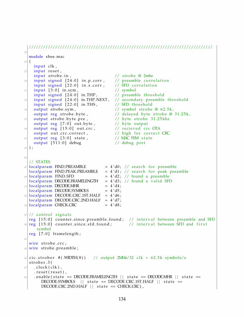
/////////////////////////////////////////////////////////////////////////////23
module xbee mac25 (
input clk ,27 input r e s e t ,
input s t r o b e i n , // s t rob e @ 2mhz29 input signed [ 2 4 : 0 ] i n p c o r r , // preamble c o r r e l a t i o n
input signed [ 2 2 : 0 ] i n s c o r r , // SFD c o r r e l a t i o n31 input [ 3 : 0 ] in sym , // symbol
input signed [ 2 4 : 0 ] in THP , // preamble threshold33 input signed [ 2 4 : 0 ] in THP NEXT , // secondary preamble threshold
input signed [ 2 2 : 0 ] in THS , // SFD threshold35 output strobe sym , // symbol s t robe @ 6 2 . 5 k ,
output reg s t robe byte , // delayed byte s t rob e @ 31 .25 k ,37 output s t r o b e b y t e p r e , // byte s t r obe 31 .25 khz
output reg [ 7 : 0 ] out byte , // byte output39 output reg [ 1 5 : 0 ] out crc , // rec ieved c r c OTA
output o u t c r c c o r r e c t , // high f o r c o r r e c t CRC41 output reg [ 3 : 0 ] s t a t e , // MAC FSM s t a t e
output [ 5 1 1 : 0 ] debug // debug port43 ) ;
45
// STATES47 localparam FIND PREAMBLE = 4 ’ d0 ; // search f o r preamble
localparam FIND PEAK PREAMBLE = 4 ’ d1 ; // search f o r peak preamble49 localparam FIND SFD = 4 ’ d2 ; // found a preamble
localparam DECODE FRAMELENGTH = 4 ’ d3 ; // found a va l id SFD51 localparam DECODE MHR = 4 ’ d4 ;
localparam DECODE SYMBOLS = 4 ’ d5 ;53 localparam DECODE CRC 1ST HALF = 4 ’ d6 ;
localparam DECODE CRC 2ND HALF = 4 ’ d7 ;55 localparam CHECK CRC = 4 ’ d8 ;
57 // c o n t r o l s i g n a l sreg [ 1 5 : 0 ] counter s ince preamble found ; // i n t e r v a l between preamble and SFD
59 reg [ 1 5 : 0 ] c o u n t e r s i n c e s f d f o u n d ; // i n t e r v a l between SFD and f i r s tsymbol
reg [ 7 : 0 ] framelength ;61
wire s t r o b e c r c ;63 wire strobe preamble ;
65 c i c s t r o b e r # ( .WIDTH( 8 ) ) // output 2MHz/32 c l k = 6 2 . 5 k symbols/ss t r o b e r 3 (
67 . c lock ( c l k ) ,. r e s e t ( r e s e t ) ,
69 . enable ( s t a t e == DECODE FRAMELENGTH | | s t a t e == DECODE MHR | | s t a t e ==DECODE SYMBOLS | | s t a t e == DECODE CRC 1ST HALF | | s t a t e ==DECODE CRC 2ND HALF | | s t a t e == CHECK CRC) ,
134

. r a t e ( 3 2 ) ,71 . s t r o b e f a s t ( s t r o b e i n ) ,
. s t robe s low ( strobe sym )73 ) ;
75 c i c s t r o b e r # ( .WIDTH( 8 ) ) // output 6 2 . 5 k sym/s ∗ 4 b i t /sym = 250 k b i t /s// 250 k b i t s /s = 31 .25B/s
77 s t r o b e r 4 (. c lock ( c l k ) ,
79 . r e s e t ( r e s e t ) ,. enable ( s t a t e == DECODE SYMBOLS | | s t a t e == DECODE MHR | | s t a t e ==
DECODE CRC 1ST HALF | | s t a t e == DECODE CRC 2ND HALF | | s t a t e ==CHECK CRC) ,
81 . r a t e ( 2 ) ,. s t r o b e f a s t ( strobe sym ) ,
83 . s t robe s low ( s t r o b e b y t e p r e )) ;
85
c i c s t r o b e r # ( .WIDTH( 8 ) ) // s t r o b e r @ 250khz87 s t r o b e r 5 (
. c lock ( c l k ) ,89 . r e s e t ( r e s e t ) ,
. enable ( s t a t e == DECODE MHR | | s t a t e == DECODE SYMBOLS | | s t a t e ==DECODE CRC 1ST HALF) ,
91 . r a t e ( 8 ) ,. s t r o b e f a s t ( s t r o b e i n ) ,
93 . s t robe s low ( s t r o b e c r c )) ;
95
c i c s t r o b e r # ( .WIDTH( 8 ) ) // output 2MHz/32 c l k = 6 2 . 5 k f o r f inding peakpreamble
97 s t r o b e r 6 (. c lock ( c l k ) ,
99 . r e s e t ( r e s e t ) ,. enable ( s t a t e == FIND PEAK PREAMBLE) ,
101 . r a t e ( 3 2 ) ,. s t r o b e f a s t ( s t r o b e i n ) ,
103 . s t robe s low ( strobe preamble )) ;
105
// byte s t ro be107 always @( posedge c l k ) begin
i f ( r e s e t ) begin109 s t r o b e b y t e <= 0 ;
end111 e l s e begin
s t r o b e b y t e <= s t r o b e b y t e p r e ;113 end
end115
// Preamble and SFD thresholds
135
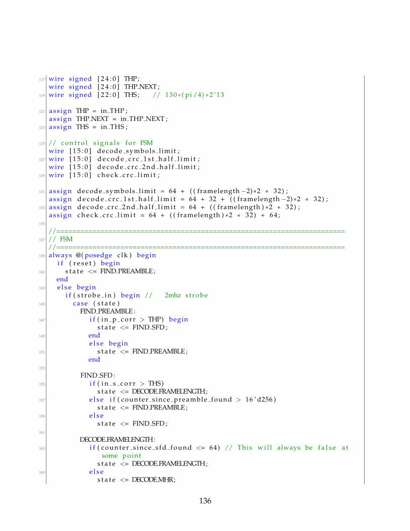
117 wire signed [ 2 4 : 0 ] THP;wire signed [ 2 4 : 0 ] THP NEXT ;
119 wire signed [ 2 2 : 0 ] THS ; // 130∗ ( pi /4) ∗2ˆ13
121 ass ign THP = in THP ;ass ign THP NEXT = in THP NEXT ;
123 ass ign THS = in THS ;
125 // c o n t r o l s i g n a l s f o r FSMwire [ 1 5 : 0 ] decode symbols l imit ;
127 wire [ 1 5 : 0 ] d e c o d e c r c 1 s t h a l f l i m i t ;wire [ 1 5 : 0 ] d e c o d e c r c 2 n d h a l f l i m i t ;
129 wire [ 1 5 : 0 ] c h e c k c r c l i m i t ;
131 ass ign decode symbols l imit = 64 + ( ( framelength−2)∗2 ∗ 32) ;ass ign d e c o d e c r c 1 s t h a l f l i m i t = 64 + 32 + ( ( framelength−2)∗2 ∗ 32) ;
133 ass ign d e c o d e c r c 2 n d h a l f l i m i t = 64 + ( ( framelength ) ∗2 ∗ 32) ;ass ign c h e c k c r c l i m i t = 64 + ( ( framelength ) ∗2 ∗ 32) + 6 4 ;
135
//========================================================================137 // FSM
//========================================================================139 always @( posedge c l k ) begin
i f ( r e s e t ) begin141 s t a t e <= FIND PREAMBLE ;
end143 e l s e begin
i f ( s t r o b e i n ) begin // 2mhz s t rob e145 case ( s t a t e )
FIND PREAMBLE :147 i f ( i n p c o r r > THP) begin
s t a t e <= FIND SFD ;149 end
e l s e begin151 s t a t e <= FIND PREAMBLE ;
end153
FIND SFD :155 i f ( i n s c o r r > THS)
s t a t e <= DECODE FRAMELENGTH;157 e l s e i f ( counter s ince preamble found > 16 ’ d256 )
s t a t e <= FIND PREAMBLE ;159 e l s e
s t a t e <= FIND SFD ;161
DECODE FRAMELENGTH:163 i f ( c o u n t e r s i n c e s f d f o u n d <= 64) // This w i l l always be f a l s e a t
some points t a t e <= DECODE FRAMELENGTH;
165 e l s es t a t e <= DECODE MHR;
136

167
DECODE MHR:169 i f ( c o u n t e r s i n c e s f d f o u n d <= 64 + 704 /∗ =11( bytes ) ∗2(sym/byte ) ∗32(
chips/sym) ∗/ )s t a t e <= DECODE MHR;
171 e l s es t a t e <= DECODE SYMBOLS;
173
DECODE SYMBOLS:175 i f ( c o u n t e r s i n c e s f d f o u n d <= decode symbols l imit )
s t a t e <= DECODE SYMBOLS;177 e l s e
s t a t e <= DECODE CRC 1ST HALF ;179
DECODE CRC 1ST HALF :181 i f ( c o u n t e r s i n c e s f d f o u n d <= d e c o d e c r c 1 s t h a l f l i m i t )
s t a t e <= DECODE CRC 1ST HALF ;183 e l s e
s t a t e <= DECODE CRC 2ND HALF ;185
DECODE CRC 2ND HALF :187 i f ( c o u n t e r s i n c e s f d f o u n d <= d e c o d e c r c 2 n d h a l f l i m i t )
s t a t e <= DECODE CRC 2ND HALF ;189 e l s e
s t a t e <= CHECK CRC;191
CHECK CRC:193 i f ( c o u n t e r s i n c e s f d f o u n d <= c h e c k c r c l i m i t ) begin
s t a t e <= CHECK CRC;195 end
e l s e begin197 s t a t e <= FIND PREAMBLE ;
end199 endcase
end201 end
end203
//=========================================================205 // counters between preamble and SFD s t a t e s
//=========================================================207 // s t a r t counting i f preamble found
always @( posedge c l k )209 begin
i f ( r e s e t ) begin211 counter s ince preamble found <= 9 ’ d0 ;
end213 e l s e i f ( s t r o b e i n ) begin // 2mhz
begin215 i f ( s t a t e == FIND SFD )
counter s ince preamble found <= counter s ince preamble found + 9 ’ d1 ;
137

217 e l s ecounter s ince preamble found <= 9 ’ d0 ;
219 endend
221 end
223 // s t a r t counting i f sfd foundalways @( posedge c l k )
225 begini f ( r e s e t )
227 c o u n t e r s i n c e s f d f o u n d <= 0 ;e l s e i f ( s t r o b e i n ) begin // 2mhz
229 i f ( s t a t e == DECODE FRAMELENGTH | | s t a t e == DECODE MHR | | s t a t e ==DECODE SYMBOLS | | s t a t e == DECODE CRC 1ST HALF | | s t a t e ==DECODE CRC 2ND HALF | | s t a t e == CHECK CRC)
c o u n t e r s i n c e s f d f o u n d <= c o u n t e r s i n c e s f d f o u n d + 1 ;231 e l s e
c o u n t e r s i n c e s f d f o u n d <= 0 ;233 end
end235
// save framelength237 always @( posedge c l k )
begin239 i f ( r e s e t )
framelength <= 8 ’ b0111 1111 ;241 e l s e i f ( strobe sym & s t a t e == DECODE FRAMELENGTH) begin
framelength [ 7 : 4 ] <= in sym ;243 framelength [ 3 : 0 ] <= framelength [ 7 : 4 ] ;
end245
// f i x framelength i f bigger than max allowed247 i f ( framelength >= 8 ’ b0111 1111 && s t a t e == DECODE MHR)
framelength <= 8 ’ b0111 1111 ;249 end
251 // save bytealways @( posedge c l k )
253 begini f ( r e s e t )
255 out byte [ 7 : 0 ] <= 0 ;e l s e i f ( strobe sym & ( s t a t e == DECODE SYMBOLS | | s t a t e == DECODE MHR) ) begin
257 out byte [ 7 : 4 ] <= in sym ;out byte [ 3 : 0 ] <= out byte [ 7 : 4 ] ;
259 endend
261
// save CRC263 always @( posedge c l k )
begin265 i f ( r e s e t )
138

o u t c r c [ 1 5 : 0 ] <= 0 ;267 e l s e i f ( strobe sym & ( s t a t e == DECODE CRC 1ST HALF | | s t a t e ==
DECODE CRC 2ND HALF) ) begino u t c r c [ 1 5 : 1 2 ] <= in sym ;
269 o u t c r c [ 1 1 : 8 ] <= o u t c r c [ 1 5 : 1 2 ] ;o u t c r c [ 7 : 4 ] <= o u t c r c [ 1 1 : 8 ] ;
271 o u t c r c [ 3 : 0 ] <= o u t c r c [ 7 : 4 ] ;end
273 end
275 // count between symbolsreg [ 1 : 0 ] counter between symbols ;
277
always @( posedge c l k )279 begin
i f ( r e s e t )281 counter between symbols <= 0 ;
e l s e i f ( ( s t a t e == DECODE MHR | | s t a t e == DECODE SYMBOLS | | s t a t e ==DECODE CRC 1ST HALF) ) begin
283 i f ( s t r o b e c r c ) begincounter between symbols <= counter between symbols + 1 ;
285 endend
287 end
289 // r e g i s t e r symbolreg [ 3 : 0 ] pers i s tent sym ;
291 always @( posedge c l k ) begini f ( r e s e t )
293 pers i s tent sym <= 0 ;e l s e i f ( ( s t a t e == DECODE MHR | | s t a t e == DECODE SYMBOLS) ) begin
295 i f ( strobe sym ) beginpers i s tent sym <= in sym [ 3 : 0 ] ;
297 endend
299 e l s e i f ( s t a t e == FIND PREAMBLE | | s t a t e == FIND SFD )pers i s tent sym <= 0 ;
301 end
303 // delayed s t r o b e c r c f o r the mul t ip lexerreg s t r o b e c r c d e l a y e d ;
305 always @( posedge c l k ) begini f ( r e s e t ) begin
307 s t r o b e c r c d e l a y e d <= 0 ;end
309 e l s es t r o b e c r c d e l a y e d <= s t r o b e c r c ;
311 end
313 reg i n p u t b i t ;// mul t ip lexer
139

315 always @( counter between symbols ) begini f ( r e s e t ) begin
317 i n p u t b i t <= 0 ;end
319 e l s e i f ( ( s t a t e == DECODE MHR | | s t a t e == DECODE SYMBOLS | | s t a t e ==DECODE CRC 1ST HALF) ) begin
i f ( s t r o b e c r c d e l a y e d ) begin321 i f ( counter between symbols == 0)
i n p u t b i t <= pers i s tent sym [ 0 ] ; // get i t from input323 e l s e i f ( counter between symbols == 1)
i n p u t b i t <= pers i s tent sym [ 1 ] ; // get i t froms ym bo l p er s i s t en t
325 e l s e i f ( counter between symbols == 2)i n p u t b i t <= pers i s tent sym [ 2 ] ;
327 e l s e i f ( counter between symbols == 3)i n p u t b i t <= pers i s tent sym [ 3 ] ;
329 endend
331 e l s ei n p u t b i t <= 0 ;
333 end
335 // CRC16wire [ 1 5 : 0 ] output crc ;
337 crc16 u crc16 (. c l k ( c l k ) ,
339 . ce ( s t r o b e c r c d e l a y e d & ( s t a t e == DECODE MHR | | s t a t e == DECODE SYMBOLS | |s t a t e == DECODE CRC 1ST HALF) ) ,
. r e s e t ( r e s e t | | s t a t e == FIND PREAMBLE | | s t a t e == FIND SFD ) ,341 . i n p u t b i t ( i n p u t b i t ) ,
. output crc ( output crc )343 ) ;
345 // s t ro be i f CRC i s c o r r e c tass ign o u t c r c c o r r e c t = ( s t a t e == CHECK CRC && ( o u t c r c == output crc ) ) ;
347
// debug port349 ass ign debug = { out crc , output crc } ;
351 endmodule
src/rx/xbee mac.v
140

Appendix B
Verilog Source Code for IEEE 802.15.4Transmitter on USRP N210’s FPGA
B.1 Top Level Transmitter
1 ‘ t i m e s c a l e 1 ns / 1 ns/////////////////////////////////////////////////////////////////////////////
3 // Company : Wireless @ VT// Author : Jeong−O Jeong
5 //// Date : 10/30/2011
7 // Design Name:// Filename : zb ieee 802 15 4 mod . v
9 // P r o j e c t Name:// Target Devices :
11 // Tool vers ions :// Descr ipt ion : Top f i l e f o r IEEE 8 0 2 . 1 5 . 4 Transmit ter
13 //// Dependencies :
15 //// Revision :
17 // Revision 0 . 0 1 − F i l e Created// Addit ional Comments :
19 ///////////////////////////////////////////////////////////////////////////////
21
module zb ieee 802 15 4 mod23 #( parameter WIDTH=32)
(25 input clk ,
input ce ,27 input r s t ,
input [ 7 : 0 ] byte , // input byte to be modulated
141

29 output [WIDTH−1:0] qpsk pulse , // baseband qpsk pulseoutput [WIDTH−1:0] oqpsk pulse , // baseband oqpsk pulse
31 input s t r o b e i n , // input s t ro be @ 4 MHzoutput s t r o b e t x , // output s t r obe @ byte r a t e
33 output strobe out qpsk sym , // qpsk symbol s t robeoutput s t r o b e o u t c h i p s // chip s t r obe
35 ) ;
37
wire [ 3 : 0 ] b i tpos ;39 wire [ 3 1 : 0 ] pulse ;
wire [ 3 1 : 0 ] pulse delayed ;41 wire [ 1 : 0 ] chunk ;
wire [ 3 1 : 0 ] chip ;43 wire [ 1 5 : 0 ] iphase , qphase , iphase delayed , qphase delayed ;
wire [WIDTH−1:0] output data ;45 wire [WIDTH−1:0] symbol ;
47 ass ign qpsk pulse = pulse ;ass ign oqpsk pulse = pulse delayed ;
49
ass ign iphase = pulse [ 3 1 : 1 6 ] ;51 ass ign qphase = pulse [ 1 5 : 0 ] ;
ass ign iphase delayed = pulse delayed [ 3 1 : 1 6 ] ;53 ass ign qphase delayed = pulse delayed [ 1 5 : 0 ] ;
55 wire s t r o b e o u t p u l s e ;wire s t r o b e i n b y t e ;
57
// FIFO s i g n a l s59 wire f u l l 1 , empty 1 ;
wire f u l l 2 , empty 2 ;61 wire f u l l 3 , empty 3 ;
wire f u l l 4 , empty 4 ;63 wire f u l l 5 , empty 5 ;
wire f u l l 6 , empty 6 ;65
ass ign s t r o b e t x = s t r o b e i n b y t e ; // s t robe @ byte r a t e67 ass ign s t r o b e o u t p u l s e = s t r o b e i n ; // s t r o b e t x from d s p t x c o r e @ 4 MHz
69 // input 4 MHz, output 1 MHz st ro bec i c s t r o b e r # ( .WIDTH( 8 ) )
71 s t r o b e r 2 (. c lock ( c l k ) ,
73 . r e s e t ( r s t ) ,. enable ( 1 ’ b1 ) ,
75 . r a t e ( 4 ) ,. s t r o b e f a s t ( s t r o b e o u t p u l s e ) ,
77 . s t robe s low ( strobe out qpsk sym )) ;
79
142
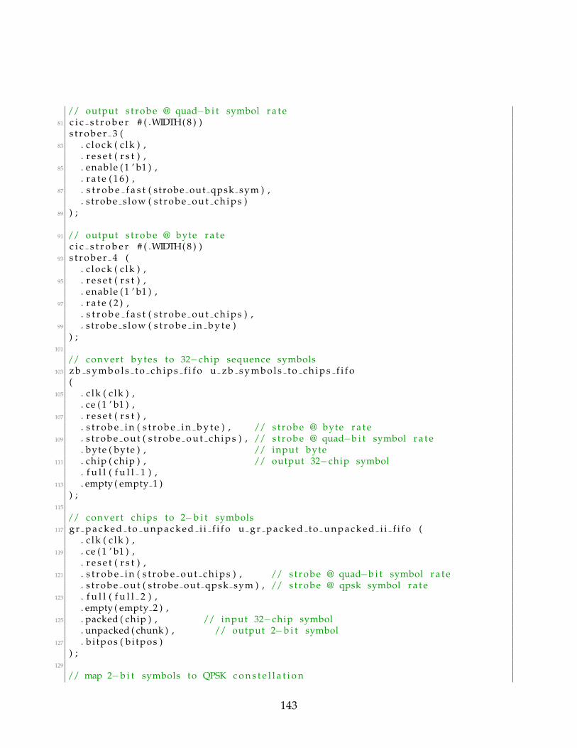
// output s t ro be @ quad−b i t symbol r a t e81 c i c s t r o b e r # ( .WIDTH( 8 ) )
s t r o b e r 3 (83 . c lock ( c l k ) ,
. r e s e t ( r s t ) ,85 . enable ( 1 ’ b1 ) ,
. r a t e ( 1 6 ) ,87 . s t r o b e f a s t ( strobe out qpsk sym ) ,
. s t robe s low ( s t r o b e o u t c h i p s )89 ) ;
91 // output s t ro be @ byte r a t ec i c s t r o b e r # ( .WIDTH( 8 ) )
93 s t r o b e r 4 (. c lock ( c l k ) ,
95 . r e s e t ( r s t ) ,. enable ( 1 ’ b1 ) ,
97 . r a t e ( 2 ) ,. s t r o b e f a s t ( s t r o b e o u t c h i p s ) ,
99 . s t robe s low ( s t r o b e i n b y t e )) ;
101
// convert bytes to 32−chip sequence symbols103 z b s y m b o l s t o c h i p s f i f o u z b s y m b o l s t o c h i p s f i f o
(105 . c l k ( c l k ) ,
. ce ( 1 ’ b1 ) ,107 . r e s e t ( r s t ) ,
. s t r o b e i n ( s t r o b e i n b y t e ) , // s t rob e @ byte r a t e109 . s t r o b e o u t ( s t r o b e o u t c h i p s ) , // s t ro be @ quad−b i t symbol r a t e
. byte ( byte ) , // input byte111 . chip ( chip ) , // output 32−chip symbol
. f u l l ( f u l l 1 ) ,113 . empty ( empty 1 )
) ;115
// convert chips to 2−b i t symbols117 g r p a c k e d t o u n p a c k e d i i f i f o u g r p a c k e d t o u n p a c k e d i i f i f o (
. c l k ( c l k ) ,119 . ce ( 1 ’ b1 ) ,
. r e s e t ( r s t ) ,121 . s t r o b e i n ( s t r o b e o u t c h i p s ) , // s t r obe @ quad−b i t symbol r a t e
. s t r o b e o u t ( strobe out qpsk sym ) , // s t robe @ qpsk symbol r a t e123 . f u l l ( f u l l 2 ) ,
. empty ( empty 2 ) ,125 . packed ( chip ) , // input 32−chip symbol
. unpacked ( chunk ) , // output 2−b i t symbol127 . b i tpos ( b i tpos )
) ;129
// map 2−b i t symbols to QPSK c o n s t e l l a t i o n
143
131 g r c h u n k s t o s y m b o l s i c f i f o u g r c h u n k s t o s y m b o l s i c f i f o (. c l k ( c l k ) , // f a s t e s t c l k 100 MHz
133 . ce ( 1 ’ b1 ) ,. s t r o b e i n ( strobe out qpsk sym ) , // s t rob e @ qpsk symbol r a t e
135 . s t r o b e o u t ( strobe out qpsk sym ) , // s t robe @ qpsk symbol r a t e. f u l l ( f u l l 3 ) ,
137 . empty ( empty 3 ) ,. r e s e t ( r s t ) ,
139 . chunk ( chunk ) , // input 2−b i t symbol. symbol ( symbol ) // output qpsk c o n s t e l l a t i o n symbol
141 ) ;
143 // upsample QPSK symbols by 4s p u p s a m p l e c c f i f o # ( . L ( 4 ) )
145 u sp up sa mp le cc f i fo(
147 . c l k ( c l k ) ,. ce ( 1 ’ b1 ) ,
149 . r e s e t ( r s t ) ,. s t r o b e i n ( strobe out qpsk sym ) , // s t rob e @ qpsk symbol r a t e
151 . s t r o b e o u t ( s t r o b e o u t p u l s e ) , // s t rob e @ 4 MHz. f u l l ( f u l l 4 ) ,
153 . empty ( empty 4 ) ,. input data ( symbol ) , // complex qpsk symbol
155 . output data ( output data ) // output upsampled qpsk symbol) ;
157
// hal f−s i n pulse shaper159 // z b h a l f s i n p u l s e n o m u l t f i f o u z b h a l f s i n p u l s e n o m u l t f i f o
z b h a l f s i n p u l s e f i f o u z b h a l f s i n p u l s e n o m u l t f i f o161 (
. c l k ( c l k ) ,163 . ce ( 1 ’ b1 ) ,
. r e s e t ( r s t ) ,165 . s t r o b e i n ( s t r o b e o u t p u l s e ) , // 4 MHz st rob e
. s t r o b e o u t ( s t r o b e o u t p u l s e ) , // 4 MHz s t rob e167 . f u l l ( f u l l 5 ) ,
. empty ( empty 5 ) ,169 . symbol ( output data ) , // 32 b i t , 16−b i t in−phase , 16−b i t q−phase
. out ( pulse ) // output 32 b i t I and Q baseband pulse171 ) ;
173 // delay quadarture to make QPSK to O−QPSKz b d e l a y c c f i f o u z b d e l a y c c f i f o
175 (. c l k ( c l k ) ,
177 . ce ( 1 ’ b1 ) ,. r e s e t ( r s t ) ,
179 . s t r o b e i n ( s t r o b e o u t p u l s e ) , // 4 MHz st rob e. s t r o b e o u t ( s t r o b e o u t p u l s e ) , // 4 MHz s t rob e
181 . f u l l ( f u l l 6 ) ,
144

. empty ( empty 6 ) ,183 . input data ( pulse ) ,
. output data ( pulse delayed )185 ) ;
187 endmodule
src/tx/zb ieee 802 15 4 mod.v
B.2 Symbols to Chips
1 ‘ t i m e s c a l e 1 ns / 1 ns/////////////////////////////////////////////////////////////////////////////
3 // Company : Wireless @ VT// Author : Jeong−O Jeong
5 //// Date : 10/17/2011
7 // Design Name:// Filename : z b s y m b o l s t o c h i p s f i f o . v
9 // P r o j e c t Name:// Target Devices :
11 // Tool vers ions :// Descr ipt ion : Map quad−b i t s to chips
13 //// Dependencies :
15 //// Revision :
17 // Revision 0 . 0 1 − F i l e Created// Addit ional Comments :
19 ///////////////////////////////////////////////////////////////////////////////
21 module z b s y m b o l s t o c h i p s f i f o(
23 input clk ,input ce ,
25 input s t r o b e i n , // s t rob e @ byte r a t einput s t robe out , // s t rob e @ symbol r a t e
27 input r e s e t ,input [ 7 : 0 ] byte , // input byte
29 output reg [ 3 1 : 0 ] chip , // output chip sequenceoutput f u l l , // FIFO f u l l
31 output empty // FIFO empty) ;
33
// s t o r e upper and lower 4 b i t s35 wire [ 3 : 0 ] lower ;
wire [ 3 : 0 ] upper ;37
145

// s i g n a l to switch between upper and lower 4 b i t s39 reg msb or lsb ;
41 // FIFO s i g n a l swire [ 3 1 : 0 ] dout ;
43 wire wr en , rd en ;ass ign wr en = s t r o b e i n && ˜ f u l l ;
45 ass ign rd en = s t r o b e i n && ˜ empty ;
47 // f i f o to s t o r e inputf i f o g e n e r a t o r v 6 2 f i f o (
49 . r s t ( r e s e t ) ,. wr clk ( c l k ) ,
51 . r d c l k ( c l k ) ,. din ( byte ) ,
53 . wr en ( wr en ) ,. rd en ( rd en ) ,
55 . dout ( dout ) ,. f u l l ( f u l l ) ,
57 . empty ( empty )) ;
59
// switch between upper and lower 4 b i t s61 always @( posedge c l k ) begin
i f ( r e s e t ) begin63 msb or lsb <= 0 ;
end65 e l s e i f ( s t r o b e i n )
msb or lsb <= 0 ;67 e l s e i f ( s t r o b e o u t ) begin
msb or lsb <= ˜ msb or lsb ;69 end
end71
// s p l i t i n t o lower and upper 4 b i t s73 ass ign lower = dout [ 3 : 0 ] ;
ass ign upper = dout [ 7 : 4 ] ;75
// lower 4 b i t s f i r s t77 // map 4 b i t s to chips
always @( msb or lsb or lower or upper ) begin79 i f ( r e s e t )
chip <= 0 ;81 e l s e begin
i f ( ˜ msb or lsb ) begin83 case ( lower )
0 : chip <= 3653456430 ;85 1 : chip <= 3986437410 ;
2 : chip <= 786023250 ;87 3 : chip <= 585997365 ;
4 : chip <= 1378802115 ;
146
89 5 : chip <= 891481500 ;6 : chip <= 3276943065 ;
91 7 : chip <= 2620728045 ;8 : chip <= 2358642555 ;
93 9 : chip <= 3100205175 ;1 0 : chip <= 2072811015 ;
95 1 1 : chip <= 2008598880 ;1 2 : chip <= 125537430 ;
97 1 3 : chip <= 1618458825 ;1 4 : chip <= 2517072780 ;
99 1 5 : chip <= 3378542520 ;d e f a u l t : chip <= 0 ;
101 endcaseend
103 e l s e begincase ( upper )
105 0 : chip <= 3653456430 ;1 : chip <= 3986437410 ;
107 2 : chip <= 786023250 ;3 : chip <= 585997365 ;
109 4 : chip <= 1378802115 ;5 : chip <= 891481500 ;
111 6 : chip <= 3276943065 ;7 : chip <= 2620728045 ;
113 8 : chip <= 2358642555 ;9 : chip <= 3100205175 ;
115 1 0 : chip <= 2072811015 ;1 1 : chip <= 2008598880 ;
117 1 2 : chip <= 125537430 ;1 3 : chip <= 1618458825 ;
119 1 4 : chip <= 2517072780 ;1 5 : chip <= 3378542520 ;
121 d e f a u l t : chip <= 0 ;endcase
123 endend
125 end
127 endmodule
src/tx/zb symbols to chips fifo.v
B.3 GNU Radio Packed to Unpacked
1 ‘ t i m e s c a l e 1 ns / 1 ns/////////////////////////////////////////////////////////////////////////////
3 // Company : Wireless @ VT// Author : Jeong−O Jeong
147

5 //// Date : 09/19/2011
7 // Design Name:// Filename : g r p a c k e d t o u n p a c k e d i i f i f o . v
9 // P r o j e c t Name:// Target Devices :
11 // Tool vers ions :// Descr ipt ion : break 32−chip sequence i n t o 16 2−b i t symbols
13 //// Dependencies :
15 //// Revision :
17 // Revision 0 . 0 1 − F i l e Created// Addit ional Comments :
19 ///////////////////////////////////////////////////////////////////////////////
21
module g r p a c k e d t o u n p a c k e d i i f i f o23 #( parameter BITS PER CHUNK=2)
(25 input clk ,
input ce ,27 input r e s e t ,
input s t r o b e i n , // s t ro be @ quad−b i t symbol r a t e29 input s t robe out , // s t rob e @ qpsk symbol r a t e
output f u l l , // FIFO f u l l31 output empty , // FIFO empty
input [ 3 1 : 0 ] packed , // 32−chip sequence33 output reg [BITS PER CHUNK−1:0] unpacked , // 2−chip symbol
output reg [ 3 : 0 ] b i tpos // 0−15 bi−chip p o s i t i o n35 ) ;
37 // output of FIFO ( chip sequence )wire [ 3 1 : 0 ] dout ;
39
// ASSUME MSB, 2 b i t s per chunk41 // unpacked
always @( b i tpos or dout or r e s e t ) begin43 i f ( r e s e t )
unpacked <= 0 ;45 e l s e begin
case ( b i tpos )47 0 : unpacked <= dout [ 3 1 : 3 0 ] ;
1 : unpacked <= dout [ 2 9 : 2 8 ] ;49 2 : unpacked <= dout [ 2 7 : 2 6 ] ;
3 : unpacked <= dout [ 2 5 : 2 4 ] ;51 4 : unpacked <= dout [ 2 3 : 2 2 ] ;
5 : unpacked <= dout [ 2 1 : 2 0 ] ;53 6 : unpacked <= dout [ 1 9 : 1 8 ] ;
7 : unpacked <= dout [ 1 7 : 1 6 ] ;55 8 : unpacked <= dout [ 1 5 : 1 4 ] ;
148
9 : unpacked <= dout [ 1 3 : 1 2 ] ;57 1 0 : unpacked <= dout [ 1 1 : 1 0 ] ;
1 1 : unpacked <= dout [ 9 : 8 ] ;59 1 2 : unpacked <= dout [ 7 : 6 ] ;
1 3 : unpacked <= dout [ 5 : 4 ] ;61 1 4 : unpacked <= dout [ 3 : 2 ] ;
1 5 : unpacked <= dout [ 1 : 0 ] ;63 endcase
end65 end
67 // FIFO s i g n a l swire wr en , rd en ;
69 ass ign wr en = s t r o b e i n && ˜ f u l l ;ass ign rd en = s t r o b e i n && ˜ empty ;
71
// FIFO to s t o r e input73 f i f o g e n e r a t o r v 6 2 f i f o (
. r s t ( r e s e t ) ,75 . wr clk ( c l k ) ,
. r d c l k ( c l k ) ,77 . din ( packed ) ,
. wr en ( wr en ) ,79 . rd en ( rd en ) ,
. dout ( dout ) ,81 . f u l l ( f u l l ) ,
. empty ( empty )83 ) ;
85 // bi tpos// c o n t r o l which two chips out of 32 chips to map to output
87 always @( posedge c l k or posedge r e s e t or posedge s t r o b e i n ) begini f ( r e s e t )
89 bi tpos <= 0 ;e l s e i f ( s t r o b e i n )
91 bi tpos <= 0 ;e l s e begin
93 i f ( s t r o b e o u t )b i tpos <= bi tpos + 1 ;
95 endend
97
endmodule
src/tx/gr packed to unpacked ii fifo.v
B.4 GNU Radio Chunks to Symbols
149
‘ t i m e s c a l e 1 ns / 1 ns2 /////////////////////////////////////////////////////////////////////////////
// Company : Wireless @ VT4 // Author : Jeong−O Jeong
//6 // Date : 09/19/2011
// Design Name:8 // Filename : g r c h u n k s t o s y m b o l s i c f i f o . v
// P r o j e c t Name:10 // Target Devices :
// Tool vers ions :12 // Descr ipt ion : Convert 2 b i t s i n t o QPSK symbols
//14 // Dependencies :
//16 // Revision :
// Revision 0 . 0 1 − F i l e Created18 // Addit ional Comments :
//20 /////////////////////////////////////////////////////////////////////////////
22 module g r c h u n k s t o s y m b o l s i c f i f o# ( parameter BITS PER CHUNK=2 ,
24 parameter WIDTH=32)(
26 input clk ,input ce ,
28 input r e s e t ,input s t r o b e i n , // s t rob e @ qpsk symbol r a t e
30 input s t robe out , // s t rob e @ qpsk symbol r a t eoutput f u l l , // FIFO f u l l
32 output empty , // FIFO emptyinput [BITS PER CHUNK−1:0] chunk , // 32 b i t i n t e g e r
34 output reg [WIDTH−1:0] symbol // MSB=in−phase , LSB=q−phase) ;
36
38 // FIFO s i g n a l swire [ 3 1 : 0 ] dout ;
40 wire wr en , rd en ;
42 // ASSUME QPSK// symbol
44 // −1 : 16 ’ b1111111111111111// 1 : 16 ’ b0000000000000001
46 always @( r e s e t or dout ) begini f ( r e s e t )
48 symbol <= 0 ;e l s e begin
50 case ( dout [ 1 : 0 ] )
150
0 : symbol <= 32 ’ b1000000000000000 1000000000000000 ; // −1−1 j52 1 : symbol <= 32 ’ b1000000000000000 0111111111111111 ; // −1+1 j
2 : symbol <= 32 ’ b0111111111111111 1000000000000000 ; // 1−1 j54 3 : symbol <= 32 ’ b0111111111111111 0111111111111111 ; // 1+1 j
endcase56 end
end58
// FIFO to s t o r e input60 ass ign wr en = s t r o b e i n && ˜ f u l l ;
ass ign rd en = s t r o b e i n && ˜ empty ;62
f i f o g e n e r a t o r v 6 2 f i f o (64 . r s t ( r e s e t ) ,
. wr clk ( c l k ) ,66 . r d c l k ( c l k ) ,
. din ( chunk ) ,68 . wr en ( wr en ) ,
. rd en ( rd en ) ,70 . dout ( dout ) ,
. f u l l ( f u l l ) ,72 . empty ( empty )
) ;74
endmodule
src/tx/gr chunks to symbols ic fifo.v
B.5 Upsampler K=4
1 ‘ t i m e s c a l e 1 ns / 1 ns/////////////////////////////////////////////////////////////////////////////
3 // Company : Wireless @ VT// Author : Jeong−O Jeong
5 //// Date : 10/18/2011
7 // Design Name:// Filename : s p u p s a m p l e c c f i f o
9 // P r o j e c t Name:// Target Devices :
11 // Tool vers ions :// Descr ipt ion : Upsample by a f a c t o r of 4
13 //// Dependencies :
15 //// Revision :
17 // Revision 0 . 0 1 − F i l e Created// Addit ional Comments :
151
19 ///////////////////////////////////////////////////////////////////////////////
21
module s p u p s a m p l e c c f i f o23 # ( parameter WIDTH=32 ,
parameter L=4 // upsample f a c t o r25 )
(27 input clk ,
input ce ,29 input r e s e t ,
input s t r o b e i n , // s t rob e @ qpsk symbol r a t e31 input s t robe out , // s t rob e @ 4 MHz
output f u l l ,33 output empty ,
input [WIDTH−1:0] input data , // I and Q baseband input35 output reg [WIDTH−1:0] output data // upsampled output
) ;37
wire [ 3 1 : 0 ] dout ;39 reg [ 3 1 : 0 ] counter ; // 32 b i t should be big enough
41 // counter f o r upsamplingalways @( posedge c l k or posedge r e s e t ) begin
43 i f ( r e s e t ) begincounter <= 0 ;
45 ende l s e i f ( s t r o b e i n )
47 counter <= 0 ;e l s e begin
49 i f ( s t r o b e o u t ) begini f ( counter == L−1)
51 counter <= 0 ;e l s e
53 counter <= counter + 1 ’ b1 ;end
55 endend
57
// output input sample and i n s e r t zeros f o r the r e s t59 always @( posedge c l k or posedge r e s e t ) begin
i f ( r e s e t )61 output data <= 0 ;
e l s e begin63 i f ( s t r o b e o u t ) begin
i f ( counter == 0)65 output data <= dout ;
e l s e67 output data <= 0 ;
end69 end
152
end71
// FIFO f o r input73 wire wr en , rd en ;
ass ign wr en = s t r o b e i n && ˜ f u l l ;75 ass ign rd en = s t r o b e i n && ˜ empty ;
77 f i f o g e n e r a t o r v 6 2 f i f o (. r s t ( r e s e t ) ,
79 . wr clk ( c l k ) ,. r d c l k ( c l k ) ,
81 . din ( input data ) ,. wr en ( wr en ) ,
83 . rd en ( rd en ) ,. dout ( dout ) ,
85 . f u l l ( f u l l ) ,. empty ( empty )
87 ) ;
89 endmodule
src/tx/sp upsample cc fifo.v
B.6 Half-Sine Pulse Shaper
1 ‘ t i m e s c a l e 1 ns / 1 ns/////////////////////////////////////////////////////////////////////////////
3 // Company : Wireless @ VT// Author : Jeong−O Jeong
5 //// Date : 10/07/2011
7 // Design Name:// Filename : z b h a l f s i n p u l s e f i f o . v
9 // P r o j e c t Name:// Target Devices :
11 // Tool vers ions :// Descr ipt ion : Half−s ine pulse shaper
13 //// Dependencies :
15 //// Revision :
17 // Revision 0 . 0 1 − F i l e Created// Addit ional Comments :
19 ///////////////////////////////////////////////////////////////////////////////
21 module z b h a l f s i n p u l s e f i f o# ( parameter WIDTH=32)
23 (
153
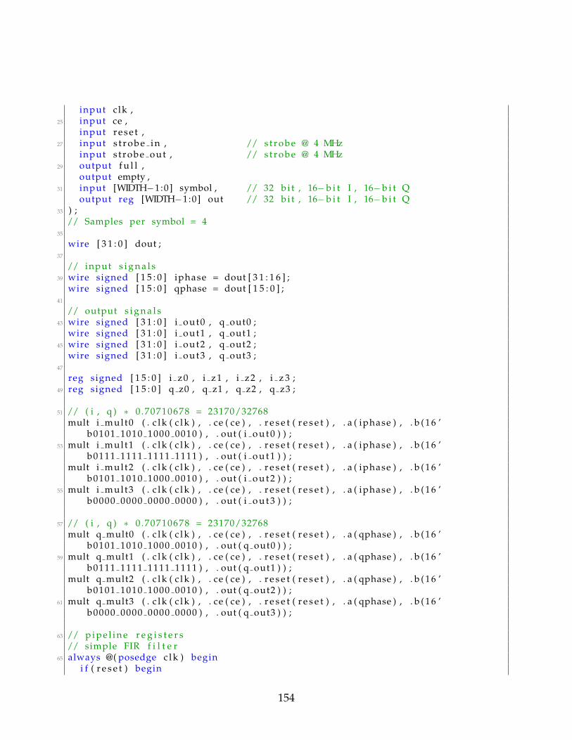
input clk ,25 input ce ,
input r e s e t ,27 input s t r o b e i n , // s t rob e @ 4 MHz
input s t robe out , // s t rob e @ 4 MHz29 output f u l l ,
output empty ,31 input [WIDTH−1:0] symbol , // 32 b i t , 16−b i t I , 16−b i t Q
output reg [WIDTH−1:0] out // 32 b i t , 16−b i t I , 16−b i t Q33 ) ;
// Samples per symbol = 435
wire [ 3 1 : 0 ] dout ;37
// input s i g n a l s39 wire signed [ 1 5 : 0 ] iphase = dout [ 3 1 : 1 6 ] ;
wire signed [ 1 5 : 0 ] qphase = dout [ 1 5 : 0 ] ;41
// output s i g n a l s43 wire signed [ 3 1 : 0 ] i out0 , q out0 ;
wire signed [ 3 1 : 0 ] i out1 , q out1 ;45 wire signed [ 3 1 : 0 ] i out2 , q out2 ;
wire signed [ 3 1 : 0 ] i out3 , q out3 ;47
reg signed [ 1 5 : 0 ] i z0 , i z1 , i z2 , i z 3 ;49 reg signed [ 1 5 : 0 ] q z0 , q z1 , q z2 , q z3 ;
51 // ( i , q ) ∗ 0 .70710678 = 23170/32768mult i mul t0 ( . c l k ( c l k ) , . ce ( ce ) , . r e s e t ( r e s e t ) , . a ( iphase ) , . b ( 1 6 ’
b0101 1010 1000 0010 ) , . out ( i o u t 0 ) ) ;53 mult i mul t1 ( . c l k ( c l k ) , . ce ( ce ) , . r e s e t ( r e s e t ) , . a ( iphase ) , . b ( 1 6 ’
b0111 1111 1111 1111 ) , . out ( i o u t 1 ) ) ;mult i mul t2 ( . c l k ( c l k ) , . ce ( ce ) , . r e s e t ( r e s e t ) , . a ( iphase ) , . b ( 1 6 ’
b0101 1010 1000 0010 ) , . out ( i o u t 2 ) ) ;55 mult i mul t3 ( . c l k ( c l k ) , . ce ( ce ) , . r e s e t ( r e s e t ) , . a ( iphase ) , . b ( 1 6 ’
b0000 0000 0000 0000 ) , . out ( i o u t 3 ) ) ;
57 // ( i , q ) ∗ 0 .70710678 = 23170/32768mult q mult0 ( . c l k ( c l k ) , . ce ( ce ) , . r e s e t ( r e s e t ) , . a ( qphase ) , . b ( 1 6 ’
b0101 1010 1000 0010 ) , . out ( q out0 ) ) ;59 mult q mult1 ( . c l k ( c l k ) , . ce ( ce ) , . r e s e t ( r e s e t ) , . a ( qphase ) , . b ( 1 6 ’
b0111 1111 1111 1111 ) , . out ( q out1 ) ) ;mult q mult2 ( . c l k ( c l k ) , . ce ( ce ) , . r e s e t ( r e s e t ) , . a ( qphase ) , . b ( 1 6 ’
b0101 1010 1000 0010 ) , . out ( q out2 ) ) ;61 mult q mult3 ( . c l k ( c l k ) , . ce ( ce ) , . r e s e t ( r e s e t ) , . a ( qphase ) , . b ( 1 6 ’
b0000 0000 0000 0000 ) , . out ( q out3 ) ) ;
63 // p i p e l i n e r e g i s t e r s// simple FIR f i l t e r
65 always @( posedge c l k ) begini f ( r e s e t ) begin
154

67 i z 0 <= 0 ;i z 1 <= 0 ;
69 i z 2 <= 0 ;end
71 e l s e begini f ( s t r o b e o u t ) begin
73 i z 0 <= i o u t 0 [ 3 1 : 1 6 ] ;i z 1 <= i z 0 + i o u t 1 [ 3 1 : 1 6 ] ;
75 i z 2 <= i z 1 + i o u t 2 [ 3 1 : 1 6 ] ;end
77 endend
79
always @( posedge c l k ) begin81 i f ( r e s e t ) begin
q z0 <= 0 ;83 q z1 <= 0 ;
q z2 <= 0 ;85 end
e l s e begin87 i f ( s t r o b e o u t ) begin
q z0 <= q out0 [ 3 1 : 1 6 ] ;89 q z1 <= q z0 + q out1 [ 3 1 : 1 6 ] ;
q z2 <= q z1 + q out2 [ 3 1 : 1 6 ] ;91 end
end93 end
95 // r e g i s t e r outputalways @( posedge c l k ) begin
97 i f ( r e s e t ) beginout <= 0 ;
99 ende l s e begin
101 i f ( s t r o b e o u t ) beginout <= { i z 2 + i o u t 3 [ 3 1 : 1 6 ] , q z2 + q out3 [ 3 1 : 1 6 ] } ;
103 endend
105 end
107 // FIFO f o r inputwire wr en , rd en ;
109 ass ign wr en = s t r o b e i n && ˜ f u l l ;ass ign rd en = s t r o b e i n && ˜ empty ;
111
f i f o g e n e r a t o r v 6 2 f i f o (113 . r s t ( r e s e t ) ,
. wr clk ( c l k ) ,115 . r d c l k ( c l k ) ,
. din ( symbol ) ,117 . wr en ( wr en ) ,
155
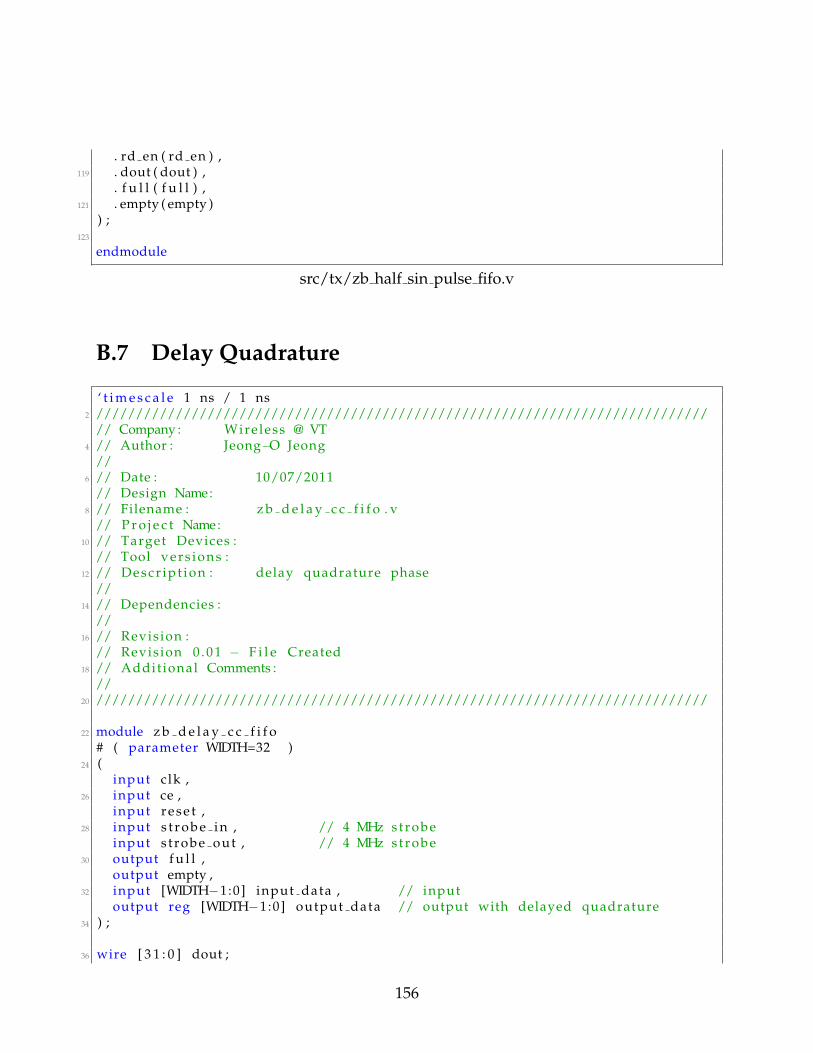
. rd en ( rd en ) ,119 . dout ( dout ) ,
. f u l l ( f u l l ) ,121 . empty ( empty )
) ;123
endmodule
src/tx/zb half sin pulse fifo.v
B.7 Delay Quadrature
‘ t i m e s c a l e 1 ns / 1 ns2 /////////////////////////////////////////////////////////////////////////////
// Company : Wireless @ VT4 // Author : Jeong−O Jeong
//6 // Date : 10/07/2011
// Design Name:8 // Filename : z b d e l a y c c f i f o . v
// P r o j e c t Name:10 // Target Devices :
// Tool vers ions :12 // Descr ipt ion : delay quadrature phase
//14 // Dependencies :
//16 // Revision :
// Revision 0 . 0 1 − F i l e Created18 // Addit ional Comments :
//20 /////////////////////////////////////////////////////////////////////////////
22 module z b d e l a y c c f i f o# ( parameter WIDTH=32 )
24 (input clk ,
26 input ce ,input r e s e t ,
28 input s t r o b e i n , // 4 MHz s t rob einput s t robe out , // 4 MHz st rob e
30 output f u l l ,output empty ,
32 input [WIDTH−1:0] input data , // inputoutput reg [WIDTH−1:0] output data // output with delayed quadrature
34 ) ;
36 wire [ 3 1 : 0 ] dout ;
156
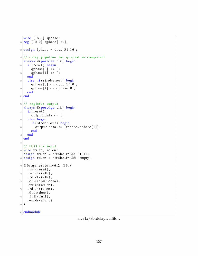
wire [ 1 5 : 0 ] iphase ;38 reg [ 1 5 : 0 ] qphase [ 0 : 1 ] ;
40 ass ign iphase = dout [ 3 1 : 1 6 ] ;
42 // delay p i p e l i n e f o r quadrature componentalways @( posedge c l k ) begin
44 i f ( r e s e t ) beginqphase [ 0 ] <= 0 ;
46 qphase [ 1 ] <= 0 ;end
48 e l s e i f ( s t r o b e o u t ) beginqphase [ 0 ] <= dout [ 1 5 : 0 ] ;
50 qphase [ 1 ] <= qphase [ 0 ] ;end
52 end
54 // r e g i s t e r outputalways @( posedge c l k ) begin
56 i f ( r e s e t )output data <= 0 ;
58 e l s e begini f ( s t r o b e o u t ) begin
60 output data <= { iphase , qphase [ 1 ] } ;end
62 endend
64
// FIFO f o r input66 wire wr en , rd en ;
ass ign wr en = s t r o b e i n && ˜ f u l l ;68 ass ign rd en = s t r o b e i n && ˜ empty ;
70 f i f o g e n e r a t o r v 6 2 f i f o (. r s t ( r e s e t ) ,
72 . wr clk ( c l k ) ,. r d c l k ( c l k ) ,
74 . din ( input data ) ,. wr en ( wr en ) ,
76 . rd en ( rd en ) ,. dout ( dout ) ,
78 . f u l l ( f u l l ) ,. empty ( empty )
80 ) ;
82 endmodule
src/tx/zb delay cc fifo.v
157
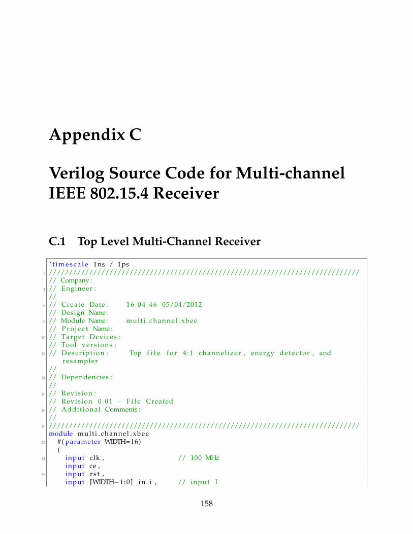
Appendix C
Verilog Source Code for Multi-channelIEEE 802.15.4 Receiver
C.1 Top Level Multi-Channel Receiver
‘ t i m e s c a l e 1ns / 1ps2 /////////////////////////////////////////////////////////////////////////////
// Company :4 // Engineer :
//6 // Create Date : 1 6 : 0 4 : 4 6 05/04/2012
// Design Name:8 // Module Name: mult i channel xbee
// P r o j e c t Name:10 // Target Devices :
// Tool vers ions :12 // Descr ipt ion : Top f i l e f o r 4 : 1 channel izer , energy detec tor , and
resampler//
14 // Dependencies ://
16 // Revision :// Revision 0 . 0 1 − F i l e Created
18 // Addit ional Comments ://
20 /////////////////////////////////////////////////////////////////////////////module mult i channel xbee
22 #( parameter WIDTH=16)(
24 input clk , // 100 MHzinput ce ,
26 input r s t ,input [WIDTH−1:0] i n i , // input I
158
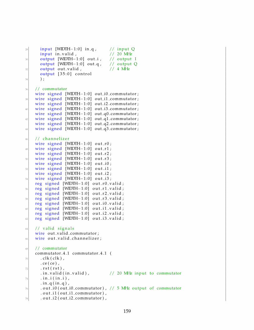
28 input [WIDTH−1:0] in q , // input Qinput i n v a l i d , // 20 MHz
30 output [WIDTH−1:0] out i , // output Ioutput [WIDTH−1:0] out q , // output Q
32 output out va l id , // 4 MHzoutput [ 3 5 : 0 ] c o n t r o l
34 ) ;
36 // commutatorwire signed [WIDTH−1:0] out i0 commutator ;
38 wire signed [WIDTH−1:0] out i1 commutator ;wire signed [WIDTH−1:0] out i2 commutator ;
40 wire signed [WIDTH−1:0] out i3 commutator ;wire signed [WIDTH−1:0] out q0 commutator ;
42 wire signed [WIDTH−1:0] out q1 commutator ;wire signed [WIDTH−1:0] out q2 commutator ;
44 wire signed [WIDTH−1:0] out q3 commutator ;
46 // channel izerwire signed [WIDTH−1:0] out r0 ;
48 wire signed [WIDTH−1:0] out r1 ;wire signed [WIDTH−1:0] out r2 ;
50 wire signed [WIDTH−1:0] out r3 ;wire signed [WIDTH−1:0] o u t i 0 ;
52 wire signed [WIDTH−1:0] o u t i 1 ;wire signed [WIDTH−1:0] o u t i 2 ;
54 wire signed [WIDTH−1:0] o u t i 3 ;reg signed [WIDTH−1:0] o u t r 0 v a l i d ;
56 reg signed [WIDTH−1:0] o u t r 1 v a l i d ;reg signed [WIDTH−1:0] o u t r 2 v a l i d ;
58 reg signed [WIDTH−1:0] o u t r 3 v a l i d ;reg signed [WIDTH−1:0] o u t i 0 v a l i d ;
60 reg signed [WIDTH−1:0] o u t i 1 v a l i d ;reg signed [WIDTH−1:0] o u t i 2 v a l i d ;
62 reg signed [WIDTH−1:0] o u t i 3 v a l i d ;
64 // val id s i g n a l swire out valid commutator ;
66 wire o u t v a l i d c h a n n e l i z e r ;
68 // commutatorcommutator 4 1 commutator 4 1 (
70 . c l k ( c l k ) ,. ce ( ce ) ,
72 . r s t ( r s t ) ,. i n v a l i d ( i n v a l i d ) , // 20 MHz input to commutator
74 . i n i ( i n i ) ,. in q ( in q ) ,
76 . o u t i 0 ( out i0 commutator ) , // 5 MHz output of commutator. o u t i 1 ( out i1 commutator ) ,
78 . o u t i 2 ( out i2 commutator ) ,
159
. o u t i 3 ( out i3 commutator ) ,80 . out q0 ( out q0 commutator ) ,
. out q1 ( out q1 commutator ) ,82 . out q2 ( out q2 commutator ) ,
. out q3 ( out q3 commutator ) ,84 . o u t v a l i d ( out valid commutator )
) ;86
// four−channel channe l izer88 channel izer4 channel izer4 (
. c l k ( c l k ) ,90 . r s t ( r s t ) ,
. ce ( ce ) ,92 . i n v a l i d ( i n v a l i d ) ,
. i n r 0 ( out i0 commutator ) , // input94 . i n r 1 ( out i1 commutator ) ,
. i n r 2 ( out i2 commutator ) ,96 . i n r 3 ( out i3 commutator ) ,
. i n i 0 ( out q0 commutator ) ,98 . i n i 1 ( out q1 commutator ) ,
. i n i 2 ( out q2 commutator ) ,100 . i n i 3 ( out q3 commutator ) ,
. out r0 ( out r0 ) , // output of each channel102 . ou t r1 ( out r1 ) ,
. out r2 ( out r2 ) ,104 . ou t r3 ( out r3 ) ,
. o u t i 0 ( o u t i 0 ) ,106 . o u t i 1 ( o u t i 1 ) ,
. o u t i 2 ( o u t i 2 ) ,108 . o u t i 3 ( o u t i 3 ) ,
. o u t v a l i d ( o u t v a l i d c h a n n e l i z e r )110 ) ;
112 // r e g i s t e r va l id output from channe l izeralways @( posedge c l k ) begin
114 i f ( r s t ) begino u t r 0 v a l i d <= 0 ;
116 o u t r 1 v a l i d <= 0 ;o u t r 2 v a l i d <= 0 ;
118 o u t r 3 v a l i d <= 0 ;o u t i 0 v a l i d <= 0 ;
120 o u t i 1 v a l i d <= 0 ;o u t i 2 v a l i d <= 0 ;
122 o u t i 3 v a l i d <= 0 ;end
124 e l s e i f ( o u t v a l i d c h a n n e l i z e r ) begino u t r 0 v a l i d <= out r0 ;
126 o u t r 1 v a l i d <= out r1 ;o u t r 2 v a l i d <= out r2 ;
128 o u t r 3 v a l i d <= out r3 ;o u t i 0 v a l i d <= o u t i 0 ;
160
130 o u t i 1 v a l i d <= o u t i 1 ;o u t i 2 v a l i d <= o u t i 2 ;
132 o u t i 3 v a l i d <= o u t i 3 ;end
134 end
136 wire [WIDTH−1:0] o u t r e n e r g y d e t e c t o r ;wire [WIDTH−1:0] o u t i e n e r g y d e t e c t o r ;
138 wire o u t v a l i d e n e r g y d e t e c t o r ;
140 // energy d e t e c t o renergydetector energydetector (
142 . c l k ( c l k ) ,. r s t ( r s t ) ,
144 . ce ( ce ) ,. i n v a l i d ( o u t v a l i d c h a n n e l i z e r ) ,
146 . i n r 0 ( out r0 ) , // input. i n r 1 ( out r1 ) ,
148 . i n r 2 ( out r2 ) ,. i n r 3 ( out r3 ) ,
150 . i n i 0 ( o u t i 0 ) ,. i n i 1 ( o u t i 1 ) ,
152 . i n i 2 ( o u t i 2 ) ,. i n i 3 ( o u t i 3 ) ,
154 . o u t r ( o u t r e n e r g y d e t e c t o r ) , // output. o u t i ( o u t i e n e r g y d e t e c t o r ) ,
156 . o u t v a l i d ( o u t v a l i d e n e r g y d e t e c t o r )) ;
158
// resampler K=4/5160 resampler 2 4 resampler 2 4 (
. c l k ( c l k ) ,162 . ce ( ce ) ,
. r s t ( r s t ) ,164 . i n v a l i d ( o u t v a l i d e n e r g y d e t e c t o r ) ,
. i n i ( o u t r e n e r g y d e t e c t o r ) , // input166 . in q ( o u t i e n e r g y d e t e c t o r ) ,
. o u t v a l i d ( o u t v a l i d ) , // output168 . o u t i ( o u t i ) ,
. out q ( out q )170 ) ;
172 endmodule
src/multi channel/multi channel xbee.v
C.2 1:4 Commutator
161
‘ t i m e s c a l e 1ns / 1ps2 /////////////////////////////////////////////////////////////////////////////
// Company : Wireless @ VT4 // Engineer : Jeong−O Jeong
//6 // Create Date : 1 6 : 1 5 : 0 1 05/04/2012
// Design Name:8 // Module Name: commutator 4 1
// P r o j e c t Name:10 // Target Devices :
// Tool vers ions :12 // Descr ipt ion : Commutator 1 : 4 , used before four−channel channe l izer
//14 // Dependencies :
//16 // Revision :
// Revision 0 . 0 1 − F i l e Created18 // Addit ional Comments :
//20 /////////////////////////////////////////////////////////////////////////////
module commutator 4 122 #( parameter WIDTH=16)
(24 input clk ,
input ce ,26 input r s t ,
input i n v a l i d ,28 input signed [WIDTH−1:0] i n i , // input
input signed [WIDTH−1:0] in q ,30 output reg signed [WIDTH−1:0] out i0 , // output a t 1/4 r a t e
output reg signed [WIDTH−1:0] out q0 ,32 output reg signed [WIDTH−1:0] out i1 ,
output reg signed [WIDTH−1:0] out q1 ,34 output reg signed [WIDTH−1:0] out i2 ,
output reg signed [WIDTH−1:0] out q2 ,36 output reg signed [WIDTH−1:0] out i3 ,
output reg signed [WIDTH−1:0] out q3 ,38 output reg o u t v a l i d
) ;40
// commutate input42 always @( posedge c l k ) begin
i f ( r s t ) begin44 o u t i 0 <= 0 ;
out q0 <= 0 ;46 o u t i 1 <= 0 ;
out q1 <= 0 ;48 o u t i 2 <= 0 ;
out q2 <= 0 ;50 o u t i 3 <= 0 ;
162

out q3 <= 0 ;52 end
e l s e i f ( ce & i n v a l i d ) begin54 o u t i 0 <= i n i ;
out q0 <= in q ;56 o u t i 1 <= o u t i 0 ;
out q1 <= out q0 ;58 o u t i 2 <= o u t i 1 ;
out q2 <= out q1 ;60 o u t i 3 <= o u t i 2 ;
out q3 <= out q2 ;62 end
end64
// counter 0−366 reg [ 1 : 0 ] counter ;
always @( posedge c l k ) begin68 i f ( r s t ) begin
counter <= 0 ;70 end
e l s e i f ( ce & i n v a l i d ) begin72 counter <= counter + 1 ’ b1 ;
end74 end
76 // output va l idalways @( posedge c l k ) begin
78 i f ( r s t ) begino u t v a l i d <= 0 ;
80 ende l s e i f ( ce ) begin
82 o u t v a l i d <= ( counter == 0) & i n v a l i d ;end
84 end
86 endmodule
src/multi channel/commutator 4 1.v
C.3 Four-Channel Channelizer
‘ t i m e s c a l e 1ns / 1ps2 /////////////////////////////////////////////////////////////////////////////
// Company : Wireless @ VT4 // Engineer : Jeong−O Jeong
//6 // Create Date : 1 5 : 0 2 : 1 3 04/27/2012
// Design Name:
163

8 // Module Name: channel izer4// P r o j e c t Name:
10 // Target Devices :// Tool vers ions :
12 // Descr ipt ion : Four−channel channe l izer with complex c o e f f i c i e n t s//
14 // Dependencies ://
16 // Revision :// Revision 0 . 0 1 − F i l e Created
18 // Addit ional Comments ://
20 /////////////////////////////////////////////////////////////////////////////module channel izer4
22 #( parameter WIDTH INPUT=16 ,parameter WIDTH OUTPUT=16)
24 (input clk ,
26 input r s t ,input ce ,
28 input i n v a l i d , // inputinput signed [WIDTH INPUT−1:0] in r0 ,
30 input signed [WIDTH INPUT−1:0] in r1 ,input signed [WIDTH INPUT−1:0] in r2 ,
32 input signed [WIDTH INPUT−1:0] in r3 ,input signed [WIDTH INPUT−1:0] i n i 0 ,
34 input signed [WIDTH INPUT−1:0] i n i 1 ,input signed [WIDTH INPUT−1:0] i n i 2 ,
36 input signed [WIDTH INPUT−1:0] i n i 3 ,output signed [WIDTH OUTPUT−1:0] out r0 , // output
38 output signed [WIDTH OUTPUT−1:0] out r1 ,output signed [WIDTH OUTPUT−1:0] out r2 ,
40 output signed [WIDTH OUTPUT−1:0] out r3 ,output signed [WIDTH OUTPUT−1:0] out i0 ,
42 output signed [WIDTH OUTPUT−1:0] out i1 ,output signed [WIDTH OUTPUT−1:0] out i2 ,
44 output signed [WIDTH OUTPUT−1:0] out i3 ,output o u t v a l i d
46 ) ;
48
// output of polyphase f i l t e r bank50 parameter WIDTH POLY OUTPUT = 1 6 ;
wire signed [WIDTH POLY OUTPUT−1:0] o u t p o l y r 0 ;52 wire signed [WIDTH POLY OUTPUT−1:0] o u t p o l y r 1 ;
wire signed [WIDTH POLY OUTPUT−1:0] o u t p o l y r 2 ;54 wire signed [WIDTH POLY OUTPUT−1:0] o u t p o l y r 3 ;
wire signed [WIDTH POLY OUTPUT−1:0] o u t p o l y i 0 ;56 wire signed [WIDTH POLY OUTPUT−1:0] o u t p o l y i 1 ;
wire signed [WIDTH POLY OUTPUT−1:0] o u t p o l y i 2 ;58 wire signed [WIDTH POLY OUTPUT−1:0] o u t p o l y i 3 ;
164
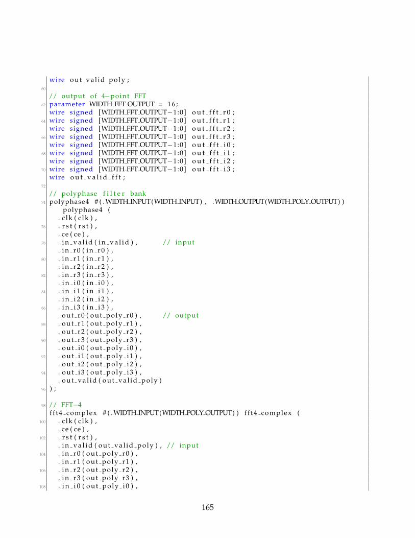
wire o u t v a l i d p o l y ;60
// output of 4−point FFT62 parameter WIDTH FFT OUTPUT = 1 6 ;
wire signed [WIDTH FFT OUTPUT−1:0] o u t f f t r 0 ;64 wire signed [WIDTH FFT OUTPUT−1:0] o u t f f t r 1 ;
wire signed [WIDTH FFT OUTPUT−1:0] o u t f f t r 2 ;66 wire signed [WIDTH FFT OUTPUT−1:0] o u t f f t r 3 ;
wire signed [WIDTH FFT OUTPUT−1:0] o u t f f t i 0 ;68 wire signed [WIDTH FFT OUTPUT−1:0] o u t f f t i 1 ;
wire signed [WIDTH FFT OUTPUT−1:0] o u t f f t i 2 ;70 wire signed [WIDTH FFT OUTPUT−1:0] o u t f f t i 3 ;
wire o u t v a l i d f f t ;72
// polyphase f i l t e r bank74 polyphase4 # ( . WIDTH INPUT(WIDTH INPUT) , .WIDTH OUTPUT(WIDTH POLY OUTPUT) )
polyphase4 (. c l k ( c l k ) ,
76 . r s t ( r s t ) ,. ce ( ce ) ,
78 . i n v a l i d ( i n v a l i d ) , // input. i n r 0 ( i n r 0 ) ,
80 . i n r 1 ( i n r 1 ) ,. i n r 2 ( i n r 2 ) ,
82 . i n r 3 ( i n r 3 ) ,. i n i 0 ( i n i 0 ) ,
84 . i n i 1 ( i n i 1 ) ,. i n i 2 ( i n i 2 ) ,
86 . i n i 3 ( i n i 3 ) ,. out r0 ( o u t p o l y r 0 ) , // output
88 . ou t r1 ( o u t p o l y r 1 ) ,. out r2 ( o u t p o l y r 2 ) ,
90 . ou t r3 ( o u t p o l y r 3 ) ,. o u t i 0 ( o u t p o l y i 0 ) ,
92 . o u t i 1 ( o u t p o l y i 1 ) ,. o u t i 2 ( o u t p o l y i 2 ) ,
94 . o u t i 3 ( o u t p o l y i 3 ) ,. o u t v a l i d ( o u t v a l i d p o l y )
96 ) ;
98 // FFT−4f f t4 complex # ( . WIDTH INPUT(WIDTH POLY OUTPUT) ) f f t4 complex (
100 . c l k ( c l k ) ,. ce ( ce ) ,
102 . r s t ( r s t ) ,. i n v a l i d ( o u t v a l i d p o l y ) , // input
104 . i n r 0 ( o u t p o l y r 0 ) ,. i n r 1 ( o u t p o l y r 1 ) ,
106 . i n r 2 ( o u t p o l y r 2 ) ,. i n r 3 ( o u t p o l y r 3 ) ,
108 . i n i 0 ( o u t p o l y i 0 ) ,
165

. i n i 1 ( o u t p o l y i 1 ) ,110 . i n i 2 ( o u t p o l y i 2 ) ,
. i n i 3 ( o u t p o l y i 3 ) ,112 . ou t r0 ( o u t f f t r 0 ) , // output
. out r1 ( o u t f f t r 1 ) ,114 . ou t r2 ( o u t f f t r 2 ) ,
. out r3 ( o u t f f t r 3 ) ,116 . o u t i 0 ( o u t f f t i 0 ) ,
. o u t i 1 ( o u t f f t i 1 ) ,118 . o u t i 2 ( o u t f f t i 2 ) ,
. o u t i 3 ( o u t f f t i 3 ) ,120 . o u t v a l i d ( o u t v a l i d f f t )
) ;122
// complex mixer f o r downconversion124 complex mixer complex mixer (
. c l k ( c l k ) ,126 . ce ( ce ) ,
. r s t ( r s t ) ,128 . i n v a l i d ( o u t v a l i d f f t ) , // input
. i n r 0 ( o u t f f t r 0 ) ,130 . i n r 1 ( o u t f f t r 1 ) ,
. i n r 2 ( o u t f f t r 2 ) ,132 . i n r 3 ( o u t f f t r 3 ) ,
. i n i 0 ( o u t f f t i 0 ) ,134 . i n i 1 ( o u t f f t i 1 ) ,
. i n i 2 ( o u t f f t i 2 ) ,136 . i n i 3 ( o u t f f t i 3 ) ,
. out r0 ( out r0 ) , // output138 . ou t r1 ( out r1 ) ,
. out r2 ( out r2 ) ,140 . ou t r3 ( out r3 ) ,
. o u t i 0 ( o u t i 0 ) ,142 . o u t i 1 ( o u t i 1 ) ,
. o u t i 2 ( o u t i 2 ) ,144 . o u t i 3 ( o u t i 3 ) ,
. o u t v a l i d ( o u t v a l i d )146 ) ;
148 endmodule
src/multi channel/channelizer4.v
C.4 Polyphase Filter Bank
‘ t i m e s c a l e 1ns / 1ps2 /////////////////////////////////////////////////////////////////////////////
// Company : Wireless @ VT
166
4 // Engineer : Jeong−O Jeong//
6 // Create Date : 1 0 : 2 1 : 5 5 04/28/2012// Design Name:
8 // Module Name: polyphase4// P r o j e c t Name:
10 // Target Devices :// Tool vers ions :
12 // Descr ipt ion : polyphase f i l t e r b a n k with complex c o e f f i c i e n t s//
14 // Dependencies ://
16 // Revision :// Revision 0 . 0 1 − F i l e Created
18 // Addit ional Comments ://
20 /////////////////////////////////////////////////////////////////////////////module polyphase4
22 #( parameter WIDTH INPUT=16 ,parameter WIDTH OUTPUT=16 ,
24 parameter WIDTH FIR OUTPUT=30)(
26 input clk ,input r s t ,
28 input ce ,input i n v a l i d ,
30 input signed [WIDTH INPUT−1:0] in r0 , // inputs t h a t are alreadycommutated
input signed [WIDTH INPUT−1:0] in r1 ,32 input signed [WIDTH INPUT−1:0] in r2 ,
input signed [WIDTH INPUT−1:0] in r3 ,34 input signed [WIDTH INPUT−1:0] i n i 0 ,
input signed [WIDTH INPUT−1:0] i n i 1 ,36 input signed [WIDTH INPUT−1:0] i n i 2 ,
input signed [WIDTH INPUT−1:0] i n i 3 ,38 output out va l id ,
output signed [WIDTH OUTPUT−1:0] out r0 , // outputs of the f i l t e r s40 output signed [WIDTH OUTPUT−1:0] out r1 ,
output signed [WIDTH OUTPUT−1:0] out r2 ,42 output signed [WIDTH OUTPUT−1:0] out r3 ,
output signed [WIDTH OUTPUT−1:0] out i0 , // outputs of the f i l t e r s44 output signed [WIDTH OUTPUT−1:0] out i1 ,
output signed [WIDTH OUTPUT−1:0] out i2 ,46 output signed [WIDTH OUTPUT−1:0] o u t i 3
) ;48
// c o n t r o l s i g n a l s f o r FIR f i l t e r s50 wire rdy r0 , r d y i 0 ;
wire rdy r1 , r d y i 1 ;52 wire rdy r2 , r d y i 2 ;
wire rdy r3 , r d y i 3 ;
167

54
wire r f d r 0 , r f d i 0 ;56 wire r f d r 1 , r f d i 1 ;
wire r f d r 2 , r f d i 2 ;58 wire r f d r 3 , r f d i 3 ;
60 // output of FIR f i l t e r swire signed [WIDTH FIR OUTPUT−1:0] dout r0 , dout i0 , dout i r0 , d o u t r i 0 ;
62 wire signed [WIDTH FIR OUTPUT−1:0] dout r1 , dout i1 , dout i r1 , d o u t r i 1 ;wire signed [WIDTH FIR OUTPUT−1:0] dout r2 , dout i2 , dout i r2 , d o u t r i 2 ;
64 wire signed [WIDTH FIR OUTPUT−1:0] dout r3 , dout i3 , dout i r3 , d o u t r i 3 ;
66 // temporary r e g i s t e r s f o r addi t ion and s u b t r a c t i o nreg signed [WIDTH FIR OUTPUT : 0 ] tmp r0 , tmp i0 ;
68 reg signed [WIDTH FIR OUTPUT : 0 ] tmp r1 , tmp i1 ;reg signed [WIDTH FIR OUTPUT : 0 ] tmp r2 , tmp i2 ;
70 reg signed [WIDTH FIR OUTPUT : 0 ] tmp r3 , tmp i3 ;reg tmp valid ;
72
// combine the output of f i l t e r s t h i s way s i n c e the f i l t e r c o e f f i e n t s arecomplex
74 always @( posedge c l k ) begini f ( r s t ) begin
76 tmp r0 <= 0 ;tmp r1 <= 0 ;
78 tmp r2 <= 0 ;tmp r3 <= 0 ;
80 tmp i0 <= 0 ;tmp i1 <= 0 ;
82 tmp i2 <= 0 ;tmp i3 <= 0 ;
84 tmp valid <= 0 ;end
86 e l s e i f ( ce ) begintmp r0 <= dout r0−dout i0 ;
88 tmp r1 <= dout r1−dout i1 ;tmp r2 <= dout r2−dout i2 ;
90 tmp r3 <= dout r3−dout i3 ;tmp i0 <= d o u t r i 0 + d o u t i r 0 ;
92 tmp i1 <= d o u t r i 1 + d o u t i r 1 ;tmp i2 <= d o u t r i 2 + d o u t i r 2 ;
94 tmp i3 <= d o u t r i 3 + d o u t i r 3 ;tmp valid <= r d y i 3 ;
96 endend
98
parameter OFFSET=0;100
// output102 ass ign out r0 = tmp r0 [WIDTH FIR OUTPUT+1−1−OFFSET : WIDTH FIR OUTPUT+1−1−
WIDTH OUTPUT+1−OFFSET ] ;
168
ass ign out r1 = tmp r1 [WIDTH FIR OUTPUT+1−1−OFFSET : WIDTH FIR OUTPUT+1−1−WIDTH OUTPUT+1−OFFSET ] ;
104 ass ign out r2 = tmp r2 [WIDTH FIR OUTPUT+1−1−OFFSET : WIDTH FIR OUTPUT+1−1−WIDTH OUTPUT+1−OFFSET ] ;
ass ign out r3 = tmp r3 [WIDTH FIR OUTPUT+1−1−OFFSET : WIDTH FIR OUTPUT+1−1−WIDTH OUTPUT+1−OFFSET ] ;
106
ass ign o u t i 0 = tmp i0 [WIDTH FIR OUTPUT+1−1−OFFSET : WIDTH FIR OUTPUT+1−1−WIDTH OUTPUT+1−OFFSET ] ;
108 ass ign o u t i 1 = tmp i1 [WIDTH FIR OUTPUT+1−1−OFFSET : WIDTH FIR OUTPUT+1−1−WIDTH OUTPUT+1−OFFSET ] ;
ass ign o u t i 2 = tmp i2 [WIDTH FIR OUTPUT+1−1−OFFSET : WIDTH FIR OUTPUT+1−1−WIDTH OUTPUT+1−OFFSET ] ;
110 ass ign o u t i 3 = tmp i3 [WIDTH FIR OUTPUT+1−1−OFFSET : WIDTH FIR OUTPUT+1−1−WIDTH OUTPUT+1−OFFSET ] ;
112 ass ign o u t v a l i d = tmp valid ;//=================================================================
114 // r e a l c o e f f i c i e n t s , r e a l inputs//=================================================================
116 f i r r e a l f i r h 0 (. c l k ( c l k ) , // input c l k
118 . ce ( ce ) , // input ce. nd ( i n v a l i d ) , // input nd
120 . f i l t e r s e l ( 2 ’ d0 ) , // input [1 : 0 ] f i l t e r s e l. r fd ( r f d r 0 ) , // ouput r fd
122 . rdy ( rdy r0 ) , // ouput rdy. din ( i n r 0 ) , // input [15 : 0 ] din 1
124 . dout ( dout r0 ) ) ; // ouput [29 : 0 ] dout 1
126 f i r r e a l f i r h 1 (. c l k ( c l k ) , // input c l k
128 . ce ( ce ) , // input ce. nd ( i n v a l i d ) , // input nd
130 . f i l t e r s e l ( 2 ’ d1 ) , // input [2 : 0 ] f i l t e r s e l. r fd ( r f d r 1 ) , // ouput r fd
132 . rdy ( rdy r1 ) , // ouput rdy. din ( i n r 1 ) , // input [15 : 0 ] din 1
134 . dout ( dout r1 ) ) ; // ouput [29 : 0 ] dout 1
136 f i r r e a l f i r h 2 (. c l k ( c l k ) , // input c l k
138 . ce ( ce ) , // input ce. nd ( i n v a l i d ) , // input nd
140 . f i l t e r s e l ( 2 ’ d2 ) , // input [2 : 0 ] f i l t e r s e l. r fd ( r f d r 2 ) , // ouput r fd
142 . rdy ( rdy r2 ) , // ouput rdy. din ( i n r 2 ) , // input [15 : 0 ] din 1
144 . dout ( dout r2 ) ) ; // ouput [29 : 0 ] dout 1
146 f i r r e a l f i r h 3 (
169

. c l k ( c l k ) , // input c l k148 . ce ( ce ) , // input ce
. nd ( i n v a l i d ) , // input nd150 . f i l t e r s e l ( 2 ’ d3 ) , // input [2 : 0 ] f i l t e r s e l
. r fd ( r f d r 3 ) , // ouput r fd152 . rdy ( rdy r3 ) , // ouput rdy
. din ( i n r 3 ) , // input [15 : 0 ] din 1154 . dout ( dout r3 ) ) ; // ouput [29 : 0 ] dout 1
156 //=================================================================// imaginary c o e f f i c i e n t s , imag inputs
158 //=================================================================f i r i m a g f i r i m a g h 0 (
160 . c l k ( c l k ) , // input c l k. ce ( ce ) , // input ce
162 . nd ( i n v a l i d ) , // input nd. f i l t e r s e l ( 2 ’ d0 ) , // input [2 : 0 ] f i l t e r s e l
164 . r fd ( r f d i 0 ) , // ouput r fd. rdy ( r d y i 0 ) , // ouput rdy
166 . din ( i n i 0 ) , // input [15 : 0 ] din 1. dout ( dout i0 ) ) ; // ouput [29 : 0 ] dout 1
168
f i r i m a g f i r i m a g h 1 (170 . c l k ( c l k ) , // input c l k
. ce ( ce ) , // input ce172 . nd ( i n v a l i d ) , // input nd
. f i l t e r s e l ( 2 ’ d1 ) , // input [2 : 0 ] f i l t e r s e l174 . r fd ( r f d i 1 ) , // ouput r fd
. rdy ( r d y i 1 ) , // ouput rdy176 . din ( i n i 1 ) , // input [15 : 0 ] din 1
. dout ( dout i1 ) ) ; // ouput [29 : 0 ] dout 1178
f i r i m a g f i r i m a g h 2 (180 . c l k ( c l k ) , // input c l k
. ce ( ce ) , // input ce182 . nd ( i n v a l i d ) , // input nd
. f i l t e r s e l ( 2 ’ d2 ) , // input [2 : 0 ] f i l t e r s e l184 . r fd ( r f d i 2 ) , // ouput r fd
. rdy ( r d y i 2 ) , // ouput rdy186 . din ( i n i 2 ) , // input [15 : 0 ] din 1
. dout ( dout i2 ) ) ; // ouput [29 : 0 ] dout 1188
f i r i m a g f i r i m a g h 3 (190 . c l k ( c l k ) , // input c l k
. ce ( ce ) , // input ce192 . nd ( i n v a l i d ) , // input nd
. f i l t e r s e l ( 2 ’ d3 ) , // input [2 : 0 ] f i l t e r s e l194 . r fd ( r f d i 3 ) , // ouput r fd
. rdy ( r d y i 3 ) , // ouput rdy196 . din ( i n i 3 ) , // input [15 : 0 ] din 1
. dout ( dout i3 ) ) ; // ouput [29 : 0 ] dout 1
170
198
//=================================================================200 // imaginary c o e f f i c i e n t s , r e a l inputs
//=================================================================202 f i r i m a g f i r i r h 0 (
. c l k ( c l k ) , // input c l k204 . ce ( ce ) , // input ce
. nd ( i n v a l i d ) , // input nd206 . f i l t e r s e l ( 2 ’ d0 ) , // input [2 : 0 ] f i l t e r s e l
. r fd ( ) , // ouput r fd208 . rdy ( ) , // ouput rdy
. din ( i n r 0 ) , // input [15 : 0 ] din 1210 . dout ( d o u t i r 0 ) ) ; // ouput [29 : 0 ] dout 1
212 f i r i m a g f i r i r h 1 (. c l k ( c l k ) , // input c l k
214 . ce ( ce ) , // input ce. nd ( i n v a l i d ) , // input nd
216 . f i l t e r s e l ( 2 ’ d1 ) , // input [2 : 0 ] f i l t e r s e l. r fd ( ) , // ouput r fd
218 . rdy ( ) , // ouput rdy. din ( i n r 1 ) , // input [15 : 0 ] din 1
220 . dout ( d o u t i r 1 ) ) ; // ouput [29 : 0 ] dout 1
222 f i r i m a g f i r i r h 2 (. c l k ( c l k ) , // input c l k
224 . ce ( ce ) , // input ce. nd ( i n v a l i d ) , // input nd
226 . f i l t e r s e l ( 2 ’ d2 ) , // input [2 : 0 ] f i l t e r s e l. r fd ( ) , // ouput r fd
228 . rdy ( ) , // ouput rdy. din ( i n r 2 ) , // input [15 : 0 ] din 1
230 . dout ( d o u t i r 2 ) ) ; // ouput [29 : 0 ] dout 1
232 f i r i m a g f i r i r h 3 (. c l k ( c l k ) , // input c l k
234 . ce ( ce ) , // input ce. nd ( i n v a l i d ) , // input nd
236 . f i l t e r s e l ( 2 ’ d3 ) , // input [2 : 0 ] f i l t e r s e l. r fd ( ) , // ouput r fd
238 . rdy ( ) , // ouput rdy. din ( i n r 3 ) , // input [15 : 0 ] din 1
240 . dout ( d o u t i r 3 ) ) ; // ouput [29 : 0 ] dout 1
242 //=================================================================// r e a l c o e f f i c i e n t s , imag inputs
244 //=================================================================f i r r e a l f i r r i h 0 (
246 . c l k ( c l k ) , // input c l k. ce ( ce ) , // input ce
248 . nd ( i n v a l i d ) , // input nd
171

. f i l t e r s e l ( 2 ’ d0 ) , // input [1 : 0 ] f i l t e r s e l250 . r fd ( ) , // ouput r fd
. rdy ( ) , // ouput rdy252 . din ( i n i 0 ) , // input [15 : 0 ] din 1
. dout ( d o u t r i 0 ) ) ; // ouput [29 : 0 ] dout 1254
f i r r e a l f i r r i h 1 (256 . c l k ( c l k ) , // input c l k
. ce ( ce ) , // input ce258 . nd ( i n v a l i d ) , // input nd
. f i l t e r s e l ( 2 ’ d1 ) , // input [2 : 0 ] f i l t e r s e l260 . r fd ( ) , // ouput r fd
. rdy ( ) , // ouput rdy262 . din ( i n i 1 ) , // input [15 : 0 ] din 1
. dout ( d o u t r i 1 ) ) ; // ouput [29 : 0 ] dout 1264
f i r r e a l f i r r i h 2 (266 . c l k ( c l k ) , // input c l k
. ce ( ce ) , // input ce268 . nd ( i n v a l i d ) , // input nd
. f i l t e r s e l ( 2 ’ d2 ) , // input [2 : 0 ] f i l t e r s e l270 . r fd ( ) , // ouput r fd
. rdy ( ) , // ouput rdy272 . din ( i n i 2 ) , // input [15 : 0 ] din 1
. dout ( d o u t r i 2 ) ) ; // ouput [29 : 0 ] dout 1274
f i r r e a l f i r r i h 3 (276 . c l k ( c l k ) , // input c l k
. ce ( ce ) , // input ce278 . nd ( i n v a l i d ) , // input nd
. f i l t e r s e l ( 2 ’ d3 ) , // input [2 : 0 ] f i l t e r s e l280 . r fd ( ) , // ouput r fd
. rdy ( ) , // ouput rdy282 . din ( i n i 3 ) , // input [15 : 0 ] din 1
. dout ( d o u t r i 3 ) ) ; // ouput [29 : 0 ] dout 1284
endmodule
src/multi channel/polyphase4.v
C.5 Four-point FFT
‘ t i m e s c a l e 1ns / 1ps2 /////////////////////////////////////////////////////////////////////////////
// Company : Wireless@VT4 // Engineer : Jeong−O Jeong
//6 // Create Date : 1 5 : 0 8 : 5 8 04/27/2012
172

// Design Name:8 // Module Name: f f t4 complex
// P r o j e c t Name:10 // Target Devices :
// Tool vers ions :12 // Descr ipt ion : Complex four−point FFT
//14 // Dependencies :
//16 // Revision :
// Revision 0 . 0 1 − F i l e Created18 // Addit ional Comments :
//20 /////////////////////////////////////////////////////////////////////////////
module f f t4 complex22 #( parameter WIDTH INPUT=16 ,
parameter WIDTH OUTPUT=16)24 (
input clk ,26 input r s t ,
input ce ,28 input i n v a l i d ,
input signed [WIDTH INPUT−1:0] in r0 , // inputs30 input signed [WIDTH INPUT−1:0] in r1 ,
input signed [WIDTH INPUT−1:0] in r2 ,32 input signed [WIDTH INPUT−1:0] in r3 ,
input signed [WIDTH INPUT−1:0] i n i 0 ,34 input signed [WIDTH INPUT−1:0] i n i 1 ,
input signed [WIDTH INPUT−1:0] i n i 2 ,36 input signed [WIDTH INPUT−1:0] i n i 3 ,
output reg signed [WIDTH OUTPUT−1:0] out r0 , // outputs38 output reg signed [WIDTH OUTPUT−1:0] out r1 ,
output reg signed [WIDTH OUTPUT−1:0] out r2 ,40 output reg signed [WIDTH OUTPUT−1:0] out r3 ,
output reg signed [WIDTH OUTPUT−1:0] out i0 ,42 output reg signed [WIDTH OUTPUT−1:0] out i1 ,
output reg signed [WIDTH OUTPUT−1:0] out i2 ,44 output reg signed [WIDTH OUTPUT−1:0] out i3 ,
output reg o u t v a l i d46 ) ;
48
// Radix 4 FFT reduces to addi t ions and s u b t a c t i o n s as the fol lowing50 wire [ 1 8 : 0 ] sum r0 = i n r 0 + i n r 1 + i n r 2 + i n r 3 ;
wire [ 1 8 : 0 ] sum r1 = i n r 0 + i n i 1 − i n r 2 − i n i 3 ;52 wire [ 1 8 : 0 ] sum r2 = i n r 0 − i n r 1 + i n r 2 − i n r 3 ;
wire [ 1 8 : 0 ] sum r3 = i n r 0 − i n i 1 − i n r 2 + i n i 3 ;54 wire [ 1 8 : 0 ] sum r4 = i n i 0 + i n i 1 + i n i 2 + i n i 3 ;
wire [ 1 8 : 0 ] sum r5 = i n i 0 − i n r 1 − i n i 2 + i n r 3 ;56 wire [ 1 8 : 0 ] sum r6 = i n i 0 − i n i 1 + i n i 2 − i n i 3 ;
wire [ 1 8 : 0 ] sum r7 = i n i 0 + i n r 1 − i n i 2 − i n r 3 ;
173
58
// R e g i s t e r outputs60 always @( posedge c l k ) begin
i f ( r s t ) begin62 out r0 <= 0 ;
out r1 <= 0 ;64 out r2 <= 0 ;
out r3 <= 0 ;66 o u t i 0 <= 0 ;
o u t i 1 <= 0 ;68 o u t i 2 <= 0 ;
o u t i 3 <= 0 ;70 o u t v a l i d <= 0 ;
end72 e l s e i f ( ce ) begin
out r0 <= sum r0 [ 1 8 : 3 ] ;74 out r1 <= sum r1 [ 1 8 : 3 ] ;
out r2 <= sum r2 [ 1 8 : 3 ] ;76 out r3 <= sum r3 [ 1 8 : 3 ] ;
o u t i 0 <= sum r4 [ 1 8 : 3 ] ;78 o u t i 1 <= sum r5 [ 1 8 : 3 ] ;
o u t i 2 <= sum r6 [ 1 8 : 3 ] ;80 o u t i 3 <= sum r7 [ 1 8 : 3 ] ;
o u t v a l i d <= i n v a l i d ;82 end
end84
endmodule
src/multi channel/fft4 complex.v
C.6 Complex Mixer
1 ‘ t i m e s c a l e 1ns / 1ps/////////////////////////////////////////////////////////////////////////////
3 // Company : Wireless @ VT// Engineer : Jeong−O Jeong
5 //// Create Date : 1 1 : 0 8 : 5 9 05/02/2012
7 // Design Name:// Module Name: complex mixer
9 // P r o j e c t Name:// Target Devices :
11 // Tool vers ions :// Descr ipt ion : Downconvert input by F =0.5
13 //// Dependencies :
15 //
174
// Revision :17 // Revision 0 . 0 1 − F i l e Created
// Addit ional Comments :19 //
/////////////////////////////////////////////////////////////////////////////21 module complex mixer
# ( parameter WIDTH INPUT=16 ,23 parameter WIDTH OUTPUT=16)
(25 input clk ,
input r s t ,27 input ce ,
input i n v a l i d , // input29 input signed [WIDTH INPUT−1:0] in r0 ,
input signed [WIDTH INPUT−1:0] in r1 ,31 input signed [WIDTH INPUT−1:0] in r2 ,
input signed [WIDTH INPUT−1:0] in r3 ,33 input signed [WIDTH INPUT−1:0] i n i 0 ,
input signed [WIDTH INPUT−1:0] i n i 1 ,35 input signed [WIDTH INPUT−1:0] i n i 2 ,
input signed [WIDTH INPUT−1:0] i n i 3 ,37 output reg signed [WIDTH OUTPUT−1:0] out r0 , // output
output reg signed [WIDTH OUTPUT−1:0] out r1 ,39 output reg signed [WIDTH OUTPUT−1:0] out r2 ,
output reg signed [WIDTH OUTPUT−1:0] out r3 ,41 output reg signed [WIDTH OUTPUT−1:0] out i0 ,
output reg signed [WIDTH OUTPUT−1:0] out i1 ,43 output reg signed [WIDTH OUTPUT−1:0] out i2 ,
output reg signed [WIDTH OUTPUT−1:0] out i3 ,45 output reg o u t v a l i d
) ;47
// toggle between 0 and 149 reg counter ;
51 always @( posedge c l k ) begini f ( r s t ) begin
53 counter <= 0 ;end
55 e l s e i f ( ce & i n v a l i d ) begincounter <= counter + 1 ’ b1 ;
57 endend
59
// Downconversion by F =0.5 i s simply f l i p p i n g the sign at every other sample61 always @( posedge c l k ) begin
i f ( r s t ) begin63 out r0 <= 0 ;
out r1 <= 0 ;65 out r2 <= 0 ;
out r3 <= 0 ;
175
67 o u t i 0 <= 0 ;o u t i 1 <= 0 ;
69 o u t i 2 <= 0 ;o u t i 3 <= 0 ;
71 o u t v a l i d <= 0 ;end
73 e l s e i f ( ce ) begino u t v a l i d <= i n v a l i d ;
75 i f ( counter ) beginout r0 <= i n r 0 ;
77 out r1 <= i n r 1 ;out r2 <= i n r 2 ;
79 out r3 <= i n r 3 ;o u t i 0 <= i n i 0 ;
81 o u t i 1 <= i n i 1 ;o u t i 2 <= i n i 2 ;
83 o u t i 3 <= i n i 3 ;end
85 e l s e beginout r0 <= −i n r 0 ;
87 out r1 <= −i n r 1 ;out r2 <= −i n r 2 ;
89 out r3 <= −i n r 3 ;o u t i 0 <= − i n i 0 ;
91 o u t i 1 <= − i n i 1 ;o u t i 2 <= − i n i 2 ;
93 o u t i 3 <= − i n i 3 ;end
95 endend
97 endmodule
src/multi channel/complex mixer.v
C.7 Energy Detector
‘ t i m e s c a l e 1ns / 1ps2 /////////////////////////////////////////////////////////////////////////////
// Company : Wireless@VT4 // Engineer : Jeong−O Jeong
//6 // Create Date : 1 4 : 4 0 : 5 9 05/09/2012
// Design Name:8 // Module Name: energydetec tor
// P r o j e c t Name:10 // Target Devices :
// Tool vers ions :12 // Descr ipt ion : simple energy d e t e c t o r
176
// outputs the channel with maximum energy based on 4consecut ive
14 // samples//
16 // Dependencies ://
18 // Revision :// Revision 0 . 0 1 − F i l e Created
20 // Addit ional Comments ://
22 /////////////////////////////////////////////////////////////////////////////module energydetector
24 #( parameter WIDTH=16)(
26 input clk ,input r s t ,
28 input ce ,input i n v a l i d , // input
30 input signed [WIDTH−1:0] in r0 ,input signed [WIDTH−1:0] in r1 ,
32 input signed [WIDTH−1:0] in r2 ,input signed [WIDTH−1:0] in r3 ,
34 input signed [WIDTH−1:0] i n i 0 ,input signed [WIDTH−1:0] i n i 1 ,
36 input signed [WIDTH−1:0] i n i 2 ,input signed [WIDTH−1:0] i n i 3 ,
38 output reg signed [WIDTH−1:0] out r , // outputoutput reg signed [WIDTH−1:0] out i ,
40 output reg signed o u t v a l i d) ;
42
reg signed [2∗WIDTH−1:0] prod r0 , prod r1 , prod r2 , prod r3 ;44 reg signed [2∗WIDTH−1:0] prod i0 , prod i1 , prod i2 , prod i3 ;
reg out va l id prod ;46
// square each r e a l and imag48 always @( posedge c l k ) begin
i f ( r s t ) begin50 prod r0 <= 0 ;
prod r1 <= 0 ;52 prod r2 <= 0 ;
prod r3 <= 0 ;54 prod i0 <= 0 ;
prod i1 <= 0 ;56 prod i2 <= 0 ;
prod i3 <= 0 ;58 out val id prod <= 0 ;
end60 e l s e i f ( ce ) begin
i f ( i n v a l i d ) begin62 prod r0 <= i n r 0 ∗ i n r 0 ;
177
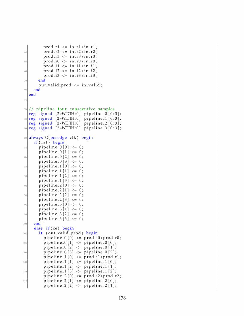
prod r1 <= i n r 1 ∗ i n r 1 ;64 prod r2 <= i n r 2 ∗ i n r 2 ;
prod r3 <= i n r 3 ∗ i n r 3 ;66 prod i0 <= i n i 0 ∗ i n i 0 ;
prod i1 <= i n i 1 ∗ i n i 1 ;68 prod i2 <= i n i 2 ∗ i n i 2 ;
prod i3 <= i n i 3 ∗ i n i 3 ;70 end
out val id prod <= i n v a l i d ;72 end
end74
76 // p i p e l i n e four consecut ive samplesreg signed [2∗WIDTH: 0 ] p i p e l i n e 0 [ 0 : 3 ] ;
78 reg signed [2∗WIDTH: 0 ] p i p e l i n e 1 [ 0 : 3 ] ;reg signed [2∗WIDTH: 0 ] p i p e l i n e 2 [ 0 : 3 ] ;
80 reg signed [2∗WIDTH: 0 ] p i p e l i n e 3 [ 0 : 3 ] ;
82 always @( posedge c l k ) begini f ( r s t ) begin
84 p i p e l i n e 0 [ 0 ] <= 0 ;p i p e l i n e 0 [ 1 ] <= 0 ;
86 p i p e l i n e 0 [ 2 ] <= 0 ;p i p e l i n e 0 [ 3 ] <= 0 ;
88 p i p e l i n e 1 [ 0 ] <= 0 ;p i p e l i n e 1 [ 1 ] <= 0 ;
90 p i p e l i n e 1 [ 2 ] <= 0 ;p i p e l i n e 1 [ 3 ] <= 0 ;
92 p i p e l i n e 2 [ 0 ] <= 0 ;p i p e l i n e 2 [ 1 ] <= 0 ;
94 p i p e l i n e 2 [ 2 ] <= 0 ;p i p e l i n e 2 [ 3 ] <= 0 ;
96 p i p e l i n e 3 [ 0 ] <= 0 ;p i p e l i n e 3 [ 1 ] <= 0 ;
98 p i p e l i n e 3 [ 2 ] <= 0 ;p i p e l i n e 3 [ 3 ] <= 0 ;
100 ende l s e i f ( ce ) begin
102 i f ( out va l id prod ) beginp i p e l i n e 0 [ 0 ] <= prod i0+prod r0 ;
104 p i p e l i n e 0 [ 1 ] <= p i p e l i n e 0 [ 0 ] ;p i p e l i n e 0 [ 2 ] <= p i p e l i n e 0 [ 1 ] ;
106 p i p e l i n e 0 [ 3 ] <= p i p e l i n e 0 [ 2 ] ;p i p e l i n e 1 [ 0 ] <= prod i1+prod r1 ;
108 p i p e l i n e 1 [ 1 ] <= p i p e l i n e 1 [ 0 ] ;p i p e l i n e 1 [ 2 ] <= p i p e l i n e 1 [ 1 ] ;
110 p i p e l i n e 1 [ 3 ] <= p i p e l i n e 1 [ 2 ] ;p i p e l i n e 2 [ 0 ] <= prod i2+prod r2 ;
112 p i p e l i n e 2 [ 1 ] <= p i p e l i n e 2 [ 0 ] ;p i p e l i n e 2 [ 2 ] <= p i p e l i n e 2 [ 1 ] ;
178
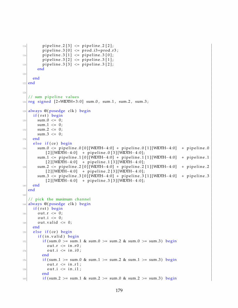
114 p i p e l i n e 2 [ 3 ] <= p i p e l i n e 2 [ 2 ] ;p i p e l i n e 3 [ 0 ] <= prod i3+prod r3 ;
116 p i p e l i n e 3 [ 1 ] <= p i p e l i n e 3 [ 0 ] ;p i p e l i n e 3 [ 2 ] <= p i p e l i n e 3 [ 1 ] ;
118 p i p e l i n e 3 [ 3 ] <= p i p e l i n e 3 [ 2 ] ;end
120
end122 end
124
// sum p i p e l i n e values126 reg signed [2∗WIDTH+ 3 : 0 ] sum 0 , sum 1 , sum 2 , sum 3 ;
128 always @( posedge c l k ) begini f ( r s t ) begin
130 sum 0 <= 0 ;sum 1 <= 0 ;
132 sum 2 <= 0 ;sum 3 <= 0 ;
134 ende l s e i f ( ce ) begin
136 sum 0 <= p i p e l i n e 0 [ 0 ] [WIDTH−4:0] + p i p e l i n e 0 [ 1 ] [WIDTH−4:0] + p i p e l i n e 0[ 2 ] [WIDTH−4:0] + p i p e l i n e 0 [ 3 ] [WIDTH−4 : 0 ] ;
sum 1 <= p i p e l i n e 1 [ 0 ] [WIDTH−4:0] + p i p e l i n e 1 [ 1 ] [WIDTH−4:0] + p i p e l i n e 1[ 2 ] [WIDTH−4:0] + p i p e l i n e 1 [ 3 ] [WIDTH−4 : 0 ] ;
138 sum 2 <= p i p e l i n e 2 [ 0 ] [WIDTH−4:0] + p i p e l i n e 2 [ 1 ] [WIDTH−4:0] + p i p e l i n e 2[ 2 ] [WIDTH−4:0] + p i p e l i n e 2 [ 3 ] [WIDTH−4 : 0 ] ;
sum 3 <= p i p e l i n e 3 [ 0 ] [WIDTH−4:0] + p i p e l i n e 3 [ 1 ] [WIDTH−4:0] + p i p e l i n e 3[ 2 ] [WIDTH−4:0] + p i p e l i n e 3 [ 3 ] [WIDTH−4 : 0 ] ;
140 endend
142
// pick the maximum channel144 always @( posedge c l k ) begin
i f ( r s t ) begin146 o u t r <= 0 ;
o u t i <= 0 ;148 o u t v a l i d <= 0 ;
end150 e l s e i f ( ce ) begin
i f ( i n v a l i d ) begin152 i f ( sum 0 >= sum 1 & sum 0 >= sum 2 & sum 0 >= sum 3 ) begin
o u t r <= i n r 0 ;154 o u t i <= i n i 0 ;
end156 i f ( sum 1 >= sum 0 & sum 1 >= sum 2 & sum 1 >= sum 3 ) begin
o u t r <= i n r 1 ;158 o u t i <= i n i 1 ;
end160 i f ( sum 2 >= sum 1 & sum 2 >= sum 0 & sum 2 >= sum 3 ) begin
179

o u t r <= i n r 2 ;162 o u t i <= i n i 2 ;
end164 i f ( sum 3 >= sum 1 & sum 3 >= sum 2 & sum 3 >= sum 0 ) begin
o u t r <= i n r 3 ;166 o u t i <= i n i 3 ;
end168 end
o u t v a l i d <= i n v a l i d ;170 end
end172
endmodule
src/multi channel/energydetector.v
C.8 Resampler 4/5
1 ‘ t i m e s c a l e 1ns / 1ps//
////////////////////////////////////////////////////////////////////////////////
3 // Company : Wireless @ VT// Engineer : Jeong−O Jeong
5 //// Create Date : 1 3 : 5 0 : 1 4 05/04/2012
7 // Design Name:// Module Name: resampler 2 4
9 // P r o j e c t Name:// Target Devices :
11 // Tool vers ions :// Descr ipt ion : Arbi t rary resampler , Max i n t e r p o l a t i o n r a t e = 2
13 //// Dependencies :
15 //// Revision :
17 // Revision 0 . 0 1 − F i l e Created// Addit ional Comments :
19 ////
////////////////////////////////////////////////////////////////////////////////
21 module resampler 2 4 (input clk ,
23 input ce ,input r s t ,
25 input i n v a l i d , // inputinput [ 1 5 : 0 ] i n i ,
180
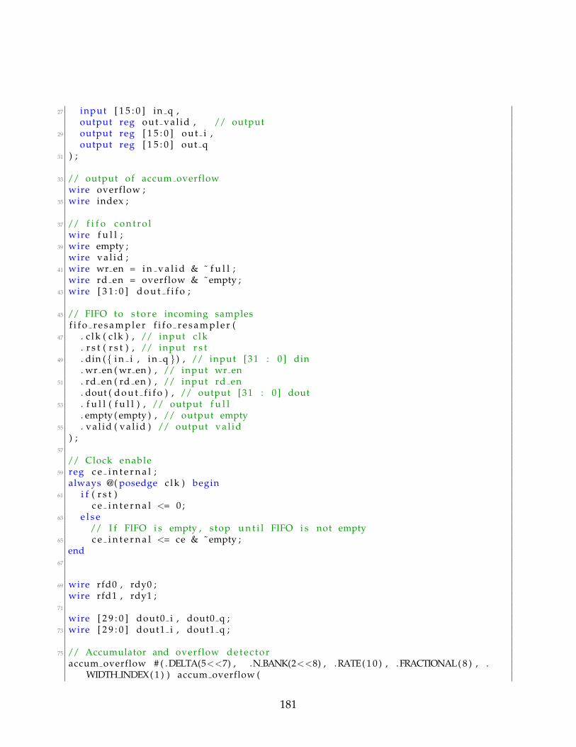
27 input [ 1 5 : 0 ] in q ,output reg out val id , // output
29 output reg [ 1 5 : 0 ] out i ,output reg [ 1 5 : 0 ] out q
31 ) ;
33 // output of accum overflowwire overflow ;
35 wire index ;
37 // f i f o c o n t r o lwire f u l l ;
39 wire empty ;wire va l id ;
41 wire wr en = i n v a l i d & ˜ f u l l ;wire rd en = overflow & ˜ empty ;
43 wire [ 3 1 : 0 ] d o u t f i f o ;
45 // FIFO to s t o r e incoming samplesf i f o r e s a m p l e r f i f o r e s a m p l e r (
47 . c l k ( c l k ) , // input c l k. r s t ( r s t ) , // input r s t
49 . din ({ i n i , in q } ) , // input [31 : 0 ] din. wr en ( wr en ) , // input wr en
51 . rd en ( rd en ) , // input rd en. dout ( d o u t f i f o ) , // output [31 : 0 ] dout
53 . f u l l ( f u l l ) , // output f u l l. empty ( empty ) , // output empty
55 . va l id ( va l id ) // output va l id) ;
57
// Clock enable59 reg c e i n t e r n a l ;
always @( posedge c l k ) begin61 i f ( r s t )
c e i n t e r n a l <= 0 ;63 e l s e
// I f FIFO i s empty , stop u n t i l FIFO i s not empty65 c e i n t e r n a l <= ce & ˜ empty ;
end67
69 wire rfd0 , rdy0 ;wire rfd1 , rdy1 ;
71
wire [ 2 9 : 0 ] dout0 i , dout0 q ;73 wire [ 2 9 : 0 ] dout1 i , dout1 q ;
75 // Accumulator and overflow d e t e c t o raccum overflow # ( .DELTA(5<<7) , .N BANK(2<<8) , .RATE( 1 0 ) , .FRACTIONAL( 8 ) , .
WIDTH INDEX( 1 ) ) accum overflow (
181
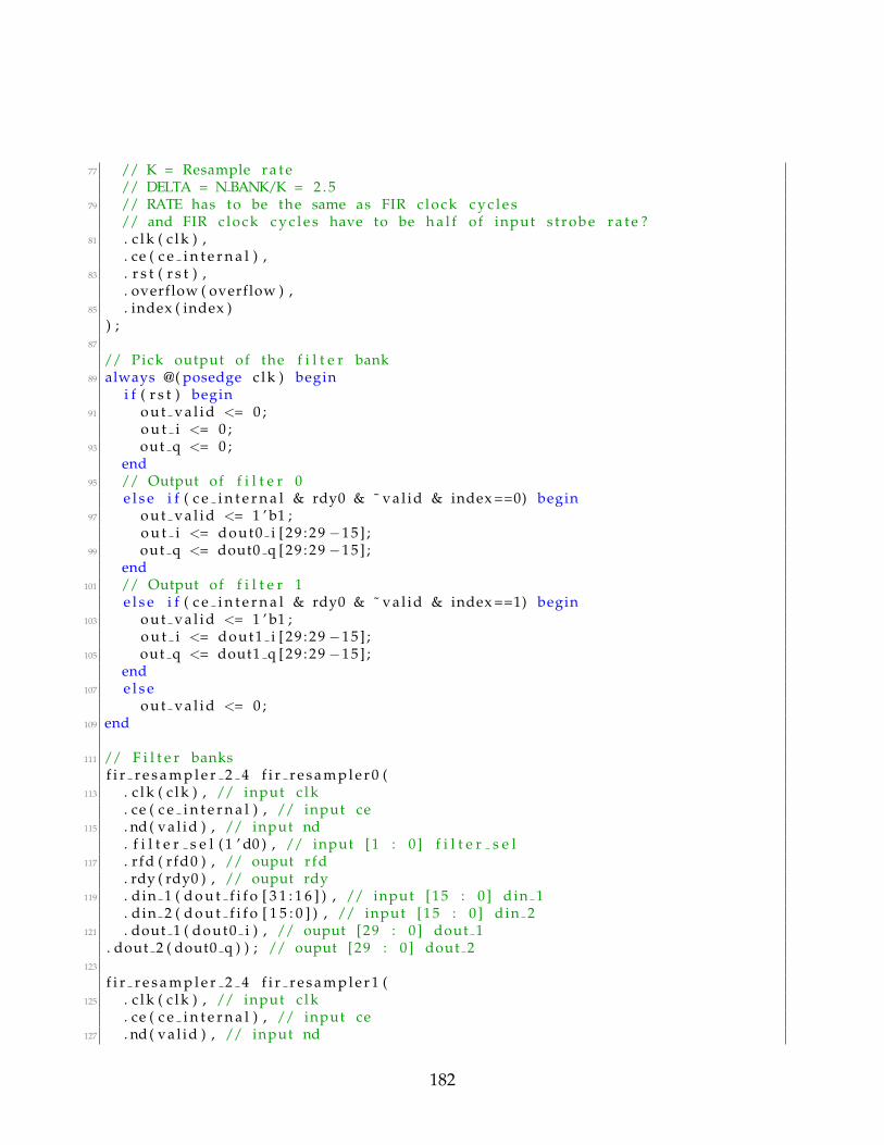
77 // K = Resample r a t e// DELTA = N BANK/K = 2 . 5
79 // RATE has to be the same as FIR c lock c y c l e s// and FIR c lock c y c l e s have to be h a l f of input s t r obe r a t e ?
81 . c l k ( c l k ) ,. ce ( c e i n t e r n a l ) ,
83 . r s t ( r s t ) ,. overflow ( overflow ) ,
85 . index ( index )) ;
87
// Pick output of the f i l t e r bank89 always @( posedge c l k ) begin
i f ( r s t ) begin91 o u t v a l i d <= 0 ;
o u t i <= 0 ;93 out q <= 0 ;
end95 // Output of f i l t e r 0
e l s e i f ( c e i n t e r n a l & rdy0 & ˜ va l id & index ==0) begin97 o u t v a l i d <= 1 ’ b1 ;
o u t i <= dout0 i [ 2 9 : 2 9 −1 5 ] ;99 out q <= dout0 q [ 2 9 : 2 9 −1 5 ] ;
end101 // Output of f i l t e r 1
e l s e i f ( c e i n t e r n a l & rdy0 & ˜ va l id & index ==1) begin103 o u t v a l i d <= 1 ’ b1 ;
o u t i <= dout1 i [ 2 9 : 2 9 −1 5 ] ;105 out q <= dout1 q [ 2 9 : 2 9 −1 5 ] ;
end107 e l s e
o u t v a l i d <= 0 ;109 end
111 // F i l t e r banksf i r r e s a m p l e r 2 4 f i r r e s a m p l e r 0 (
113 . c l k ( c l k ) , // input c l k. ce ( c e i n t e r n a l ) , // input ce
115 . nd ( va l id ) , // input nd. f i l t e r s e l ( 1 ’ d0 ) , // input [1 : 0 ] f i l t e r s e l
117 . r fd ( r fd0 ) , // ouput r fd. rdy ( rdy0 ) , // ouput rdy
119 . d in 1 ( d o u t f i f o [ 3 1 : 1 6 ] ) , // input [15 : 0 ] din 1. din 2 ( d o u t f i f o [ 1 5 : 0 ] ) , // input [15 : 0 ] din 2
121 . dout 1 ( dout0 i ) , // ouput [29 : 0 ] dout 1. dout 2 ( dout0 q ) ) ; // ouput [29 : 0 ] dout 2
123
f i r r e s a m p l e r 2 4 f i r r e s a m p l e r 1 (125 . c l k ( c l k ) , // input c l k
. ce ( c e i n t e r n a l ) , // input ce127 . nd ( va l id ) , // input nd
182
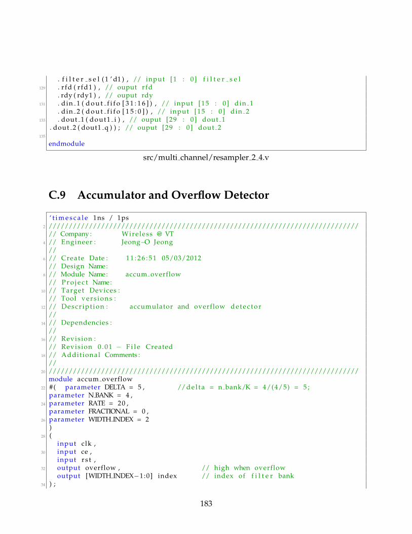
. f i l t e r s e l ( 1 ’ d1 ) , // input [1 : 0 ] f i l t e r s e l129 . r fd ( r fd1 ) , // ouput r fd
. rdy ( rdy1 ) , // ouput rdy131 . d in 1 ( d o u t f i f o [ 3 1 : 1 6 ] ) , // input [15 : 0 ] din 1
. din 2 ( d o u t f i f o [ 1 5 : 0 ] ) , // input [15 : 0 ] din 2133 . dout 1 ( dout1 i ) , // ouput [29 : 0 ] dout 1
. dout 2 ( dout1 q ) ) ; // ouput [29 : 0 ] dout 2135
endmodule
src/multi channel/resampler 2 4.v
C.9 Accumulator and Overflow Detector
‘ t i m e s c a l e 1ns / 1ps2 /////////////////////////////////////////////////////////////////////////////
// Company : Wireless @ VT4 // Engineer : Jeong−O Jeong
//6 // Create Date : 1 1 : 2 6 : 5 1 05/03/2012
// Design Name:8 // Module Name: accum overflow
// P r o j e c t Name:10 // Target Devices :
// Tool vers ions :12 // Descr ipt ion : accumulator and overflow d e t e c t o r
//14 // Dependencies :
//16 // Revision :
// Revision 0 . 0 1 − F i l e Created18 // Addit ional Comments :
//20 /////////////////////////////////////////////////////////////////////////////
module accum overflow22 #( parameter DELTA = 5 , // d e l t a = n bank/K = 4/(4/5) = 5 ;
parameter N BANK = 4 ,24 parameter RATE = 20 ,
parameter FRACTIONAL = 0 ,26 parameter WIDTH INDEX = 2
)28 (
input clk ,30 input ce ,
input r s t ,32 output overflow , // high when overflow
output [WIDTH INDEX−1:0] index // index of f i l t e r bank34 ) ;
183
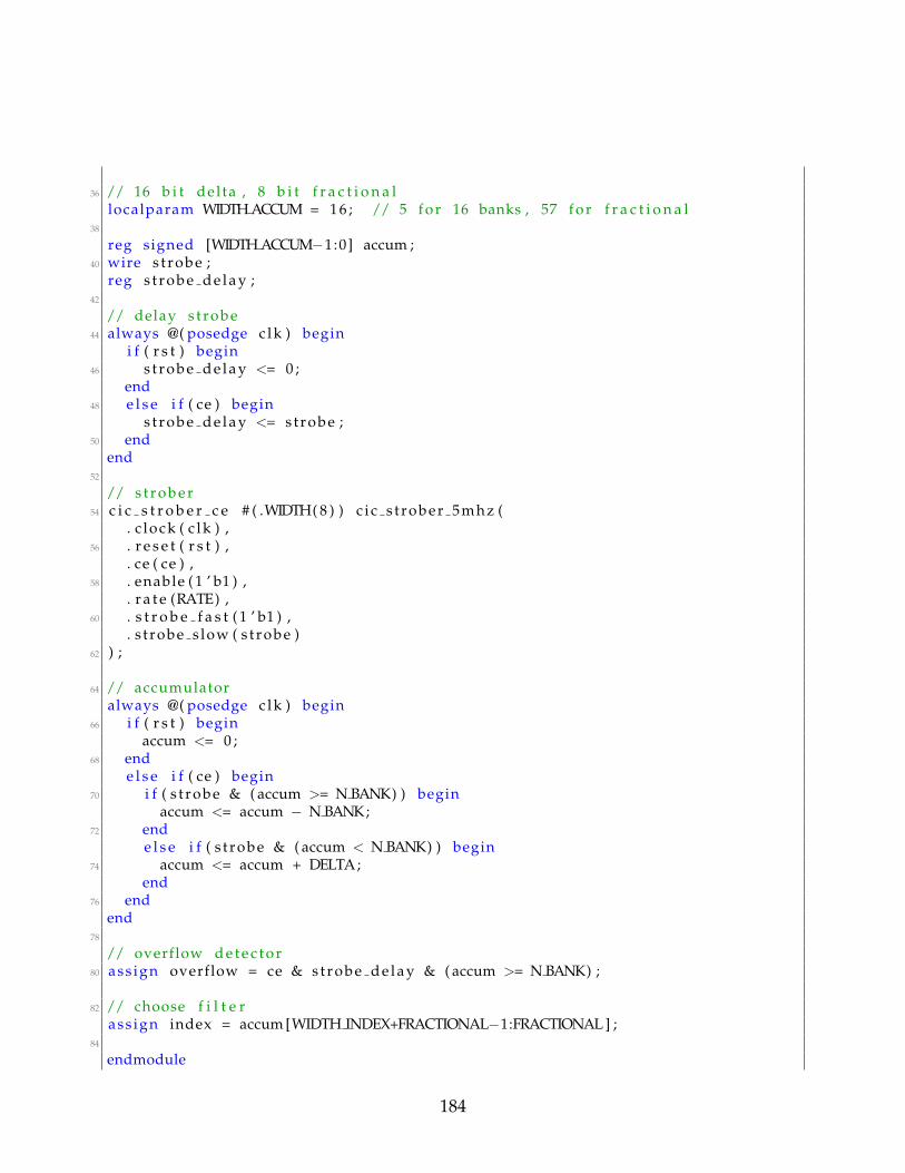
36 // 16 b i t del ta , 8 b i t f r a c t i o n a llocalparam WIDTH ACCUM = 1 6 ; // 5 f o r 16 banks , 57 f o r f r a c t i o n a l
38
reg signed [WIDTH ACCUM−1:0] accum ;40 wire s t rob e ;
reg s t r o b e d e l a y ;42
// delay s t ro be44 always @( posedge c l k ) begin
i f ( r s t ) begin46 s t r o b e d e l a y <= 0 ;
end48 e l s e i f ( ce ) begin
s t r o b e d e l a y <= s t ro be ;50 end
end52
// s t r o b e r54 c i c s t r o b e r c e # ( .WIDTH( 8 ) ) c i c s t rober 5mhz (
. c lock ( c l k ) ,56 . r e s e t ( r s t ) ,
. ce ( ce ) ,58 . enable ( 1 ’ b1 ) ,
. r a t e (RATE) ,60 . s t r o b e f a s t ( 1 ’ b1 ) ,
. s t robe s low ( s t rob e )62 ) ;
64 // accumulatoralways @( posedge c l k ) begin
66 i f ( r s t ) beginaccum <= 0 ;
68 ende l s e i f ( ce ) begin
70 i f ( s t ro be & ( accum >= N BANK) ) beginaccum <= accum − N BANK;
72 ende l s e i f ( s t robe & ( accum < N BANK) ) begin
74 accum <= accum + DELTA;end
76 endend
78
// overflow d e t e c t o r80 ass ign overflow = ce & s t r o b e d e l a y & ( accum >= N BANK) ;
82 // choose f i l t e rass ign index = accum [WIDTH INDEX+FRACTIONAL−1:FRACTIONAL ] ;
84
endmodule
184

src/multi channel/accum overflow.v
185
Appendix D
C++ Source Code for GNU Radio Blocks
D.1 GNU Radio Transmitter .h and .cc
1 /∗ −∗− c++ −∗− ∗//∗
3 ∗ Copyright 2004 Free Software Foundation , Inc .∗
5 ∗ This f i l e i s par t of GNU Radio∗
7 ∗ GNU Radio i s f r e e software ; you can r e d i s t r i b u t e i t and/or modify∗ i t under the terms of the GNU General Publ ic License as published by
9 ∗ the Free Software Foundation ; e i t h e r vers ion 3 , or ( a t your option )∗ any l a t e r vers ion .
11 ∗∗ GNU Radio i s d i s t r i b u t e d in the hope t h a t i t w i l l be useful ,
13 ∗ but WITHOUT ANY WARRANTY; without even the implied warranty of∗ MERCHANTABILITY or FITNESS FOR A PARTICULAR PURPOSE . See the
15 ∗ GNU General Publ ic License f o r more d e t a i l s .∗
17 ∗ You should have rece ived a copy of the GNU General Publ ic License∗ along with GNU Radio ; see the f i l e COPYING. I f not , wri te to
19 ∗ the Free Software Foundation , Inc . , 51 Frankl in S t r e e t ,∗ Boston , MA 02110−1301 , USA.
21 ∗/
23 // WARNING: t h i s f i l e i s machine generated . Edi t s w i l l be over wri t ten
25 # i f n d e f INCLUDED ZIGBEE SIG SOURCE C H# def ine INCLUDED ZIGBEE SIG SOURCE C H
27
# include <gr sync b lock . h>29
c l a s s z i g b e e s i g s o u r c e c ;
186
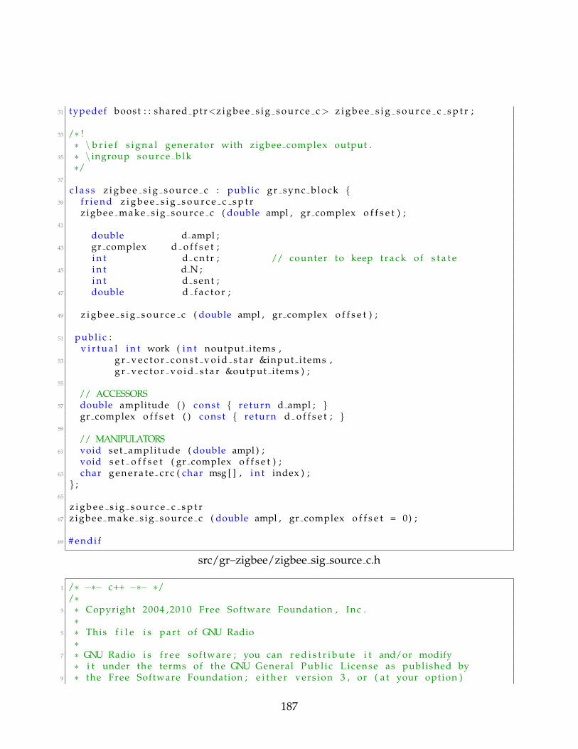
31 typedef boost : : shared ptr<z i g b e e s i g s o u r c e c> z i g b e e s i g s o u r c e c s p t r ;
33 /∗ !∗ \ b r i e f s i g n a l generator with zigbee complex output .
35 ∗ \ ingroup source b lk∗/
37
c l a s s z i g b e e s i g s o u r c e c : publ ic gr sync b lock {39 f r i e n d z i g b e e s i g s o u r c e c s p t r
z igbee make s ig source c ( double ampl , gr complex o f f s e t ) ;41
double d ampl ;43 gr complex d o f f s e t ;
i n t d c n t r ; // counter to keep t r a c k of s t a t e45 i n t d N ;
i n t d sent ;47 double d f a c t o r ;
49 z i g b e e s i g s o u r c e c ( double ampl , gr complex o f f s e t ) ;
51 publ ic :v i r t u a l i n t work ( i n t noutput items ,
53 g r v e c t o r c o n s t v o i d s t a r &input i tems ,g r v e c t o r v o i d s t a r &output i tems ) ;
55
// ACCESSORS57 double amplitude ( ) const { re turn d ampl ; }
gr complex o f f s e t ( ) const { re turn d o f f s e t ; }59
// MANIPULATORS61 void set ampl i tude ( double ampl ) ;
void s e t o f f s e t ( gr complex o f f s e t ) ;63 char g e n e r a t e c r c ( char msg [ ] , i n t index ) ;} ;
65
z i g b e e s i g s o u r c e c s p t r67 z igbee make s ig source c ( double ampl , gr complex o f f s e t = 0) ;
69 # endi f
src/gr–zigbee/zigbee sig source c.h
1 /∗ −∗− c++ −∗− ∗//∗
3 ∗ Copyright 2004 ,2010 Free Software Foundation , Inc .∗
5 ∗ This f i l e i s par t of GNU Radio∗
7 ∗ GNU Radio i s f r e e software ; you can r e d i s t r i b u t e i t and/or modify∗ i t under the terms of the GNU General Publ ic License as published by
9 ∗ the Free Software Foundation ; e i t h e r vers ion 3 , or ( a t your option )
187
∗ any l a t e r vers ion .11 ∗∗ GNU Radio i s d i s t r i b u t e d in the hope t h a t i t w i l l be useful ,
13 ∗ but WITHOUT ANY WARRANTY; without even the implied warranty of∗ MERCHANTABILITY or FITNESS FOR A PARTICULAR PURPOSE . See the
15 ∗ GNU General Publ ic License f o r more d e t a i l s .∗
17 ∗ You should have rece ived a copy of the GNU General Publ ic License∗ along with GNU Radio ; see the f i l e COPYING. I f not , wri te to
19 ∗ the Free Software Foundation , Inc . , 51 Frankl in S t r e e t ,∗ Boston , MA 02110−1301 , USA.
21 ∗/
23 // WARNING: t h i s f i l e i s machine generated . Edi t s w i l l be over wri t ten
25 # i f d e f HAVE CONFIG H# include <conf ig . h>
27 # endi f# inc lude <z i g b e e s i g s o u r c e c . h>
29 # include <algorithm># include <g r i o s i g n a t u r e . h>
31 # include <stdexcept># include <gr complex . h>
33 # include <iostream>//char msg[ ]={0 x14 , 0x61 , 0x88 , 0x5E , 0x32 , 0x33 , 0x00 , 0x00 , 0x00 , 0x00 , 0x00
, 0x00 , ’H ’ , ’E ’ , ’L ’ , ’L ’ , ’O ’ , ’ ! ’ , ’ ! ’ , ’ ! ’ } ;35 //char msg[ ]={0 x61 , 0x88 , 0xc0 , 0x32 , 0x33 , 0x0 , 0x0 , 0x0 , 0x0 , 0xa2 , 0x0 , 0
x48 , 0x45 , 0x4c , 0x4c , 0 x4f } ;// message to be transmi t ted
37 char msg[ ]={0 x41 , 0 xcc , 0xe5 , 0x78 , 0x56 , 0x22 , 0x5a , 0x63 , 0x40 , 0x00 , 0xa2 ,0x13 , 0x00 , 0x70 , 0x5a , 0x63 , 0x40 , 0x00 , 0xa2 , 0x13 , 0x00 , ’M’ , ’E ’ , ’ S ’ , ’ S’ , ’A ’ , ’G ’ , ’E ’ , ’ ’ , ’C ’ , ’O’ , ’M’ , ’ I ’ , ’N’ , ’G ’ , ’ ’ , ’ F ’ , ’R ’ , ’O’ , ’M’ , ’ ’ , ’U ’ , ’ S ’ ,’R ’ , ’P ’ , ’ ’ , ’ F ’ , ’P ’ , ’G ’ , ’A ’ ,0 x0d } ;
char chk [ ]={0 x1f , 0 xce } ; //{0xE7 , 0x3F } ;39
z i g b e e s i g s o u r c e c : : z i g b e e s i g s o u r c e c ( double ampl , gr complex o f f s e t )41 : g r sync b lock ( ” s i g s o u r c e c ” ,
gr make io s ignature ( 0 , 0 , 0 ) ,43 gr make io s ignature ( 1 , 1 , s i z e o f ( gr complex ) ) ) ,
d ampl ( ampl ) , d o f f s e t ( o f f s e t )45 {
d ampl =0;47 d c n t r =0;
d N=53; // length of packet49 d f a c t o r = 3 2 7 6 8 . 0 ;
d sent =0;51 chk [ 0 ] = g e n e r a t e c r c (msg , 0 ) ;
chk [ 1 ] = g e n e r a t e c r c (msg , 1 ) ;53 std : : cout << ”==================================” << std : : endl ;
s td : : cout << ( unsigned shor t ) ( chk [ 0 ] ) << std : : endl ;55 std : : cout << ( unsigned shor t ) ( chk [ 1 ] ) << std : : endl ;
188

std : : cout << ”==================================” << std : : endl ;57 }
59 z i g b e e s i g s o u r c e c s p t rz igbee make s ig source c ( double ampl , gr complex o f f s e t )
61 {re turn gnuradio : : g e t i n i t i a l s p t r (new z i g b e e s i g s o u r c e c ( ampl , o f f s e t ) ) ;
63 }
65 // Generate checksumchar z i g b e e s i g s o u r c e c : : g e n e r a t e c r c ( char msg [ ] , i n t index )
67 {char checksum [2]={0 x00 , 0 x00 } ;
69 char FCS [ 1 6 ] ;// i n i t i a l i z e FCS vector
71 f o r ( i n t i =0 ; i <16; i ++){FCS [ i ] = 0 ;
73 }i n t j =0 ;
75 char input ;char s0 , s1 , s2 ;
77 f o r ( i n t i =0 ; i <(d N−2) ∗8 ; i ++){
79 input = 0x01 & ( ( char )msg[ i /8] >> j ) ;s0 = input ˆ FCS [ 0 ] ;
81 s1 = s0 ˆ FCS [ 4 ] ;s2 = s0 ˆ FCS [ 1 1 ] ;
83 FCS [ 0 ] = FCS [ 1 ] ;FCS [ 1 ] = FCS [ 2 ] ;
85 FCS [ 2 ] = FCS [ 3 ] ;FCS [ 3 ] = s1 ;
87 FCS [ 4 ] = FCS [ 5 ] ;FCS [ 5 ] = FCS [ 6 ] ;
89 FCS [ 6 ] = FCS [ 7 ] ;FCS [ 7 ] = FCS [ 8 ] ;
91 FCS [ 8 ] = FCS [ 9 ] ;FCS [ 9 ] = FCS [ 1 0 ] ;
93 FCS [ 1 0 ] = s2 ;FCS [ 1 1 ] = FCS [ 1 2 ] ;
95 FCS [ 1 2 ] = FCS [ 1 3 ] ;FCS [ 1 3 ] = FCS [ 1 4 ] ;
97 FCS [ 1 4 ] = FCS [ 1 5 ] ;FCS [ 1 5 ] = s0 ;
99 j =( j +1) % 8 ;}
101
f o r ( i n t i =0 ; i <8; i ++)103 {
checksum [0 ] = checksum [ 0 ] | ( ( FCS [ i ] << i ) ) ;105 }
f o r ( i n t i =8 ; i <16; i ++)
189
107 {checksum [1 ] = checksum [ 1 ] | ( ( FCS [ i ] << ( i −8) ) ) ;
109 }/∗ std : : cout << ”==================================” << std : : endl ;
111 std : : cout << ( unsigned shor t ) (0 xFF & checksum [ 0 ] ) << std : : endl ;s td : : cout << ( unsigned shor t ) (0 xFF & checksum [ 1 ] ) << std : : endl ;
113 std : : cout << ”==================================” << std : : endl ; ∗/return checksum [ index ] ;
115 }
117 i n tz i g b e e s i g s o u r c e c : : work ( i n t noutput items ,
119 g r v e c t o r c o n s t v o i d s t a r &input i tems ,g r v e c t o r v o i d s t a r &output i tems )
121 {gr complex ∗optr = ( gr complex ∗ ) output i tems [ 0 ] ;
123 gr complex t ;
125 t = ( gr complex ) d ampl + d o f f s e t ;//=================================
127 // d ampl can be between 0 and 255//=================================
129 std : : cout << ” noutput items : ” << noutput items << std : : f l u s h << std : : endl ;f o r ( i n t i = 0 ; i < noutput items ; i ++)
131 {// preamble (4 bytes )
133 // SFD (1 bytes )// framelength (1 bytes )
135 // payload (N bytes )// FCS (2 bytes )
137
i f ( d c n t r < 4) // preamble139 d ampl = 0 ;
e l s e i f ( d c n t r < 5) // SFD141 d ampl = 1 6 7 ;
e l s e i f ( d c n t r < 6) // framelength143 d ampl = d N ;
e l s e i f ( d c n t r < 6+d N−2) // payload145 d ampl=msg[ d cntr −6] ;
e l s e i f ( d c n t r < 6+d N−1) // FCS147 d ampl=chk [ 0 ] ;
e l s e i f ( d c n t r < 6+d N ) // FCS149 {
d ampl=chk [ 1 ] ;151 }
153 // convert char i n t o complex shor toptr [ i ] = gr complex ( d ampl/ d f a c t o r , 1 .0/ d f a c t o r ) ;
155
// r e s e t i f f i n i s h e d encoding a packet157 i f ( d c n t r >= 6+d N+2)
190
d c n t r = 0 ;159 e l s e
d c n t r ++;161
}163 std : : cout << ” Generating packets . . ” << std : : f l u s h << std : : endl ;
re turn noutput items ;165 }
167 voidz i g b e e s i g s o u r c e c : : se t ampl i tude ( double ampl )
169 {// d ampl = ampl ;
171 }
173 voidz i g b e e s i g s o u r c e c : : s e t o f f s e t ( gr complex o f f s e t )
175 {d o f f s e t = o f f s e t ;
177 }
src/gr–zigbee/zigbee sig source c.cc
D.2 GNU Radio Receiver .h and .cc
# i f n d e f INCLUDED ZIGBEE RX MOD SS H2 # def ine INCLUDED ZIGBEE RX MOD SS H
4 # include <gr b lock . h># include <fstream>
6
c l a s s zigbee rx mod ss ;8
typedef boost : : shared ptr<zigbee rx mod ss> z i gbe e rx mo d ss sp t r ;10
// publ ic i n t e r f a c e f o r c r e a t i n g new i n s t a n c e s12 // howto square f f ’ s c o n s t r u c t o r i s p r i v a t e
z i gbe e rx mo d ss sp t r zigbee make rx mod ss ( s i z e t i t ems ize ) ;14
c l a s s zigbee rx mod ss : publ ic gr b lock16 {
p r i v a t e :18 // allow howto make square ff to a c c e s s the p r i v a t e c o n s t r u c t o r
// ” f r i e n d ” − once a non−member funct ion i s declared as a fr iend , i t canacess p r i v a t e data of the c l a s s
20 f r i e n d z ig bee rx mo d ss sp t r zigbee make rx mod ss ( s i z e t i t ems ize ) ;
22 zigbee rx mod ss ( s i z e t i t ems ize ) ; // p r i v a t e c o n s t r u c t o r
191
24 //enum s t a t e t {STATE FRAMELENGTH, STATE PAYLOAD, STATE CRC}// i n t d s t a t e ; // FRAMELENGTH, PAYLOAD, CRC
26 i n t d counter detec ted ;i n t d counter64 ;
28 i n t d byte counter ;i n t d t o t a l c r c c o r r e c t ;
30 i n t d t o t a l b i t s ;i n t d e r r o r b i t s ;
32 std : : ofstream d o f i l e ;s td : : ofstream d p r e a m b l e f i l e ;
34
publ ic :36 ˜ z igbee rx mod ss ( ) ; // publ ic d e s t r u c t o r
38 i n t general work ( i n t noutput items ,g r v e c t o r i n t &ninput items ,
40 g r v e c t o r c o n s t v o i d s t a r &input i tems ,g r v e c t o r v o i d s t a r &output i tems ) ;
42
} ;44
# endi f /∗ INCLUDED HOWTO SQUARE FF H ∗/
src/gr–zigbee/zigbee rx mod ss.h
# i f d e f HAVE CONFIG H2 # include ” conf ig . h”
# endi f4
# include <zigbee rx mod ss . h>6 # include <g r i o s i g n a t u r e . h>
# include <iostream>8 # include <iomanip>
# include <c s t r i n g>10 # include <s t d i o . h>
# include <fstream>12
std : : ofstream o u t p u t f i l e ;14
z i gbe e rx mo d ss sp t r zigbee make rx mod ss ( s i z e t i t ems ize )16 {
re turn z igb ee rx mo d ss sp t r (new zigbee rx mod ss ( i t ems ize ) ) ;18 }
20 s t a t i c const i n t MIN IN = 1 ;s t a t i c const i n t MAX IN = 1 ;
22 s t a t i c const i n t MIN OUT = 0 ;s t a t i c const i n t MAX OUT = 0 ;
24
// P r i v a t e c o n s t r u c t o r
192
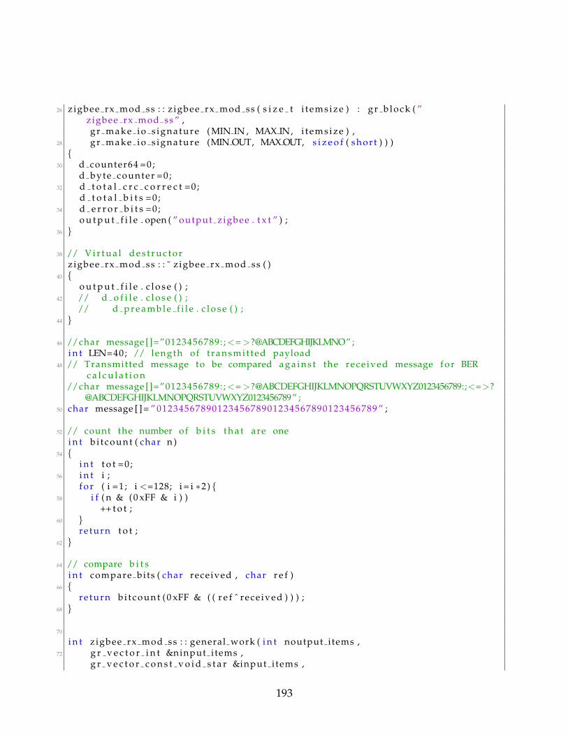
26 zigbee rx mod ss : : z igbee rx mod ss ( s i z e t i t ems ize ) : gr b lock ( ”zigbee rx mod ss ” ,gr make io s ignature ( MIN IN , MAX IN, i t em s ize ) ,
28 gr make io s ignature (MIN OUT, MAX OUT, s i z e o f ( shor t ) ) ){
30 d counter64 =0;d byte counter =0;
32 d t o t a l c r c c o r r e c t =0;d t o t a l b i t s =0;
34 d e r r o r b i t s =0;o u t p u t f i l e . open ( ” output zigbee . t x t ” ) ;
36 }
38 // V i r t u a l d e s t r u c t o rzigbee rx mod ss : : ˜ z igbee rx mod ss ( )
40 {o u t p u t f i l e . c l o s e ( ) ;
42 // d o f i l e . c l o s e ( ) ;// d p r e a m b l e f i l e . c l o s e ( ) ;
44 }
46 //char message []=”0123456789:;<=>?@ABCDEFGHIJKLMNO” ;i n t LEN=40; // length of t ransmit ted payload
48 // Transmitted message to be compared a g a i n s t the rece ived message f o r BERc a l c u l a t i o n
//char message []=”0123456789:;<=>?@ABCDEFGHIJKLMNOPQRSTUVWXYZ0123456789:;<=>?@ABCDEFGHIJKLMNOPQRSTUVWXYZ0123456789” ;
50 char message [ ] = ” 0123456789012345678901234567890123456789 ” ;
52 // count the number of b i t s t h a t are onei n t b i t cou nt ( char n )
54 {i n t t o t =0;
56 i n t i ;f o r ( i =1 ; i <=128; i = i ∗2) {
58 i f ( n & (0 xFF & i ) )++ t o t ;
60 }re turn t o t ;
62 }
64 // compare b i t si n t compare bits ( char received , char r e f )
66 {re turn b i t co un t (0 xFF & ( ( r e f ˆ rece ived ) ) ) ;
68 }
70
i n t z igbee rx mod ss : : general work ( i n t noutput items ,72 g r v e c t o r i n t &ninput items ,
g r v e c t o r c o n s t v o i d s t a r &input i tems ,
193
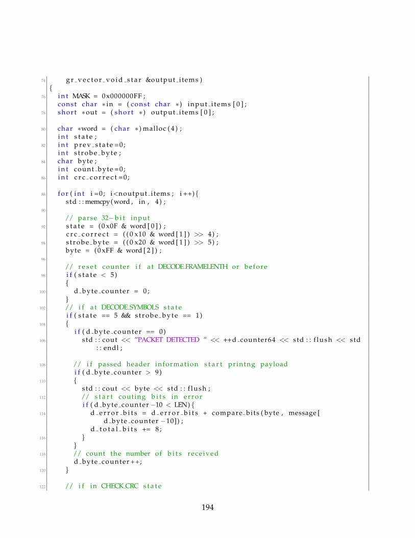
74 g r v e c t o r v o i d s t a r &output i tems ){
76 i n t MASK = 0 x000000FF ;const char ∗ in = ( const char ∗ ) input i tems [ 0 ] ;
78 shor t ∗out = ( shor t ∗ ) output i tems [ 0 ] ;
80 char ∗word = ( char ∗ ) malloc ( 4 ) ;i n t s t a t e ;
82 i n t p r e v s t a t e =0;i n t s t r o b e b y t e ;
84 char byte ;i n t count byte =0;
86 i n t c r c c o r r e c t =0;
88 f o r ( i n t i =0 ; i<noutput items ; i ++){std : : memcpy( word , in , 4 ) ;
90
// parse 32−b i t input92 s t a t e = (0 x0F & word [ 0 ] ) ;
c r c c o r r e c t = ( ( 0 x10 & word [ 1 ] ) >> 4) ;94 s t r o b e b y t e = ( ( 0 x20 & word [ 1 ] ) >> 5) ;
byte = (0 xFF & word [ 2 ] ) ;96
// r e s e t counter i f a t DECODE FRAMELENTH or before98 i f ( s t a t e < 5)
{100 d byte counter = 0 ;
}102 // i f a t DECODE SYMBOLS s t a t e
i f ( s t a t e == 5 && s t r o b e b y t e == 1)104 {
i f ( d byte counter == 0)106 std : : cout << ”PACKET DETECTED ” << ++d counter64 << std : : f l u s h << std
: : endl ;
108 // i f passed header information s t a r t printng payloadi f ( d byte counter > 9)
110 {std : : cout << byte << std : : f l u s h ;
112 // s t a r t couting b i t s in e r r o ri f ( d byte counter−10 < LEN) {
114 d e r r o r b i t s = d e r r o r b i t s + compare bits ( byte , message [d byte counter −10]) ;
d t o t a l b i t s += 8 ;116 }
}118 // count the number of b i t s rece ived
d byte counter ++;120 }
122 // i f in CHECK CRC s t a t e
194
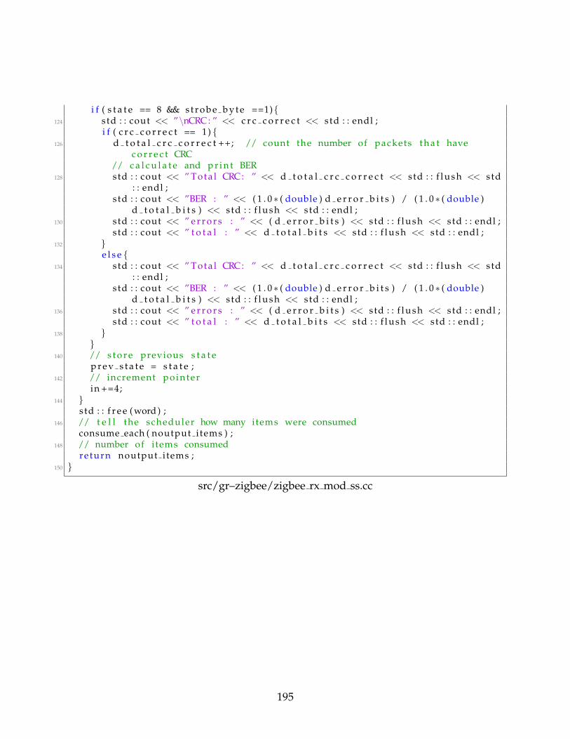
i f ( s t a t e == 8 && s t r o b e b y t e ==1){124 std : : cout << ”\nCRC: ” << c r c c o r r e c t << std : : endl ;
i f ( c r c c o r r e c t == 1) {126 d t o t a l c r c c o r r e c t ++; // count the number of packets t h a t have
c o r r e c t CRC// c a l c u l a t e and p r i n t BER
128 std : : cout << ” Tota l CRC: ” << d t o t a l c r c c o r r e c t << std : : f l u s h << std: : endl ;
s td : : cout << ”BER : ” << ( 1 . 0 ∗ ( double ) d e r r o r b i t s ) / ( 1 . 0 ∗ ( double )d t o t a l b i t s ) << std : : f l u s h << std : : endl ;
130 std : : cout << ” e r r o r s : ” << ( d e r r o r b i t s ) << std : : f l u s h << std : : endl ;s td : : cout << ” t o t a l : ” << d t o t a l b i t s << std : : f l u s h << std : : endl ;
132 }e l s e {
134 std : : cout << ” Tota l CRC: ” << d t o t a l c r c c o r r e c t << std : : f l u s h << std: : endl ;
s td : : cout << ”BER : ” << ( 1 . 0 ∗ ( double ) d e r r o r b i t s ) / ( 1 . 0 ∗ ( double )d t o t a l b i t s ) << std : : f l u s h << std : : endl ;
136 std : : cout << ” e r r o r s : ” << ( d e r r o r b i t s ) << std : : f l u s h << std : : endl ;s td : : cout << ” t o t a l : ” << d t o t a l b i t s << std : : f l u s h << std : : endl ;
138 }}
140 // s t o r e previous s t a t ep r e v s t a t e = s t a t e ;
142 // increment pointerin +=4;
144 }std : : f r e e ( word ) ;
146 // t e l l the scheduler how many items were consumedconsume each ( noutput items ) ;
148 // number of items consumedreturn noutput items ;
150 }
src/gr–zigbee/zigbee rx mod ss.cc
195