hybrid on-chip data networks - hot · pdf filehybrid on-chip data networks ... local write...
TRANSCRIPT
Hybrid On-chip Data Networks
Gilbert HendryKeren Bergman
Lightwave Research Lab
Columbia University

2
Chip-Scale Interconnection Networks
Intel Polaris IBM Cell AMD Opteron
• Chip multi-processors create need for high performance interconnects
• Performance bottleneck of on-chip networks and I/O• Power dissipation constraints of the chip package
• > 50% of total power comes from interconnects*
* N. Magen et al., “Interconnect-power dissipation in a microprocessor,” SLIP 2004.

3
Motivation
• CMPs of the future = 3D stacking• Lots of data on chip• Photonics offers
key advantages
4
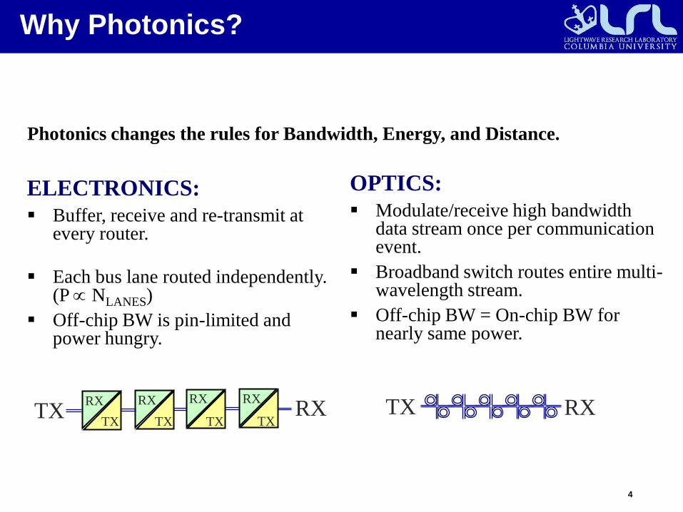
Why Photonics?
TX RX
ELECTRONICS: Buffer, receive and re-transmit at
every router.
Each bus lane routed independently. (P ∝ NLANES)
Off-chip BW is pin-limited and power hungry.
Photonics changes the rules for Bandwidth, Energy, and Distance.
OPTICS: Modulate/receive high bandwidth
data stream once per communication event.
Broadband switch routes entire multi-wavelength stream.
Off-chip BW = On-chip BW for nearly same power.
RX
TX
RX RX
TX
RX
TX RXTX TX TXTXTX TX
RX

5
Hybrid Network Premise
Optical processing difficult and limited
Source, destination routing inefficient
Use electronics for routing, optics for switching and transmission
Hybrid Circuit-Switching

6
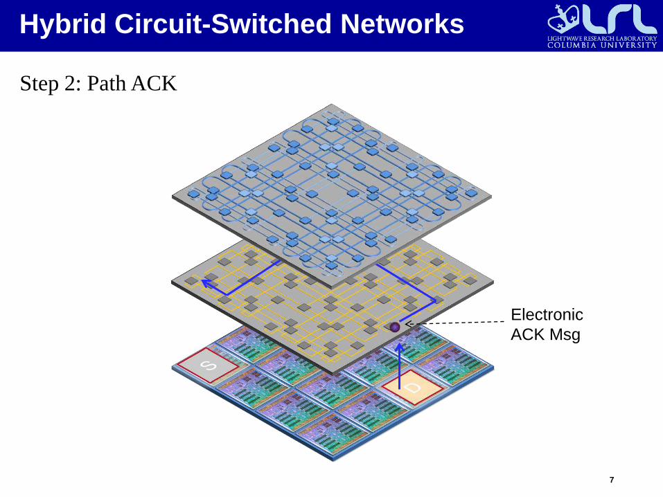
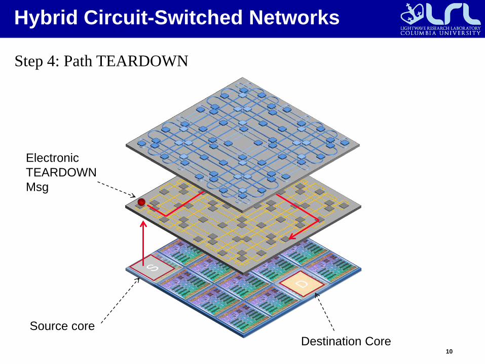
Hybrid Circuit-Switched Networks
Step 1: Path SETUP request
Electronic SETUP Msg
Source coreDestination Core
7
Hybrid Circuit-Switched Networks
Step 2: Path ACK
Electronic ACK Msg

8
Hybrid Circuit-Switched Networks
Step 3: Transmit Data
Photonic Switch Use Information

9
Hybrid Circuit-Switched Networks
Meanwhile: Path Contention
Path BLOCKED Msg(Backoff)
10
Hybrid Circuit-Switched Networks
Step 4: Path TEARDOWN
Electronic TEARDOWN Msg
Source coreDestination Core

11
Hybrid Circuit-Switched Networks
• Energy-efficient end-to-end transmission
• High bandwidth through WDM
• Electronic network still available for small control messages*
• Network-level support for secure regions
• Path setup latency• Path setup contention
(no fairness)
Pros: Cons:
* [G. Hendry et al. Analysis of Photonic Networks for a Chip Multiprocessor Using Scientific Applications. In NOCS, 2009]

Programming and Communication

13
Shared Memory
Implicit Communication
Explicit Communication
scaling
“… [ OpenMPon large systems] often performs worse than message passing due to a combination of false sharing, coherence traffic, contention, and system issues that arise from the difference in scheduling and network interface moderation”
~ ExascaleReport
14
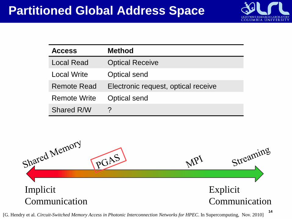
Partitioned Global Address Space
Implicit Communication
Explicit Communication
[G. Hendry et al. Circuit-Switched Memory Access in Photonic Interconnection Networks for HPEC. In Supercomputing, Nov. 2010]
Access Method
Local Read Optical Receive
Local Write Optical send
Remote Read Electronic request, optical receive
Remote Write Optical send
Shared R/W ?

15
Message Passing
Implicit Communication
Explicit Communication
* [G. Hendry et al. Analysis of Photonic Networks for a Chip Multiprocessor Using Scientific Applications. In NOCS, 2009]
• Complex, dynamic access patterns
• Relatively larger blocks of data• Scientific computing

16
Streaming
Implicit Communication
Explicit Communication
1
2
3
4
Input DataOutput Data
Persistent optical circuits
• Embedded / specialized systems (Graphics, Image + Signal Proc.)• Execution mode of general-purpose systems (Cell Processor)

Electronic Plane

18
Electronic Router
Arbiter
…
Control Router
Data Switch
Buffer Crossbar
Buffer Cntrl
Data Path
XbarCntrlRequest Bus
Flow Control
XbarAllocation
Data Switch Allocation
Routing Logic
Credits In
XbarCntrl
Ring Cntrl
Ring Cntrl
• Low frequency operation (~ 1GHz)• 1 VC (typically)• Small buffers (64-28)• Narrow Channels (8-32)

19
Network Gateway
Core
Core
Core
Core
Tx/Rx
Net
wor
k IF
Bidirectional Waveguide
Bidirectional Electronic Channel
Control RouterElectronic Crossbar
5-port photonic switch
To/From Control plane
To/From Data plane
Se
rializ
atio
n
Driv
ers
Des
eria
lizat
ion
Re
ceiv
ers
[P. Kumar et al. Exploring concentration and channel slicing in on-chip network router. In NOCS, 2009]
External Concentration

The Photonic Plane

21
Wavelength Division Multiplexing
λ
waveguide

22
Silicon Photonic Waveguide Technology
[Vlasov and McNab, Optics Express 12 (8) 1622 (2004)]
C23(1559 nm)
C28
(1555 nm)C46
(1541 nm)C51
(1537 nm)
before injection into waveguide
after 5-cm waveguide and EDFA
[B. G. Lee et al., Photon. Technol. Lett. 20 (10) 767 (2008)]
1.28 Tb/s Data Transmission Experiment(occupies small slice of available WG BW)
100 ps
Silicon photonic waveguides provide low-power optical interconnects in CMOS-compatible platform.
Low-loss (1.7 dB/cm), high-bandwidth (> 200 nm) silicon photonic waveguides can be fabricated in commercial CMOS process.

23
Ring Resonator Operation
λ
λ
modulator/filter
Broadband spatial switch

24
Silicon Photonic Modulator and Detector Technology
[M Watts, Group Four Photonics (2008)]
[M Lipson, Optics Express (2007)]
85 fJ/bit demonstrated at 10 Gb/s Scalable to < 25 fJ/bit
18 Gb/s demonstrated
[S Koester, J. Lightw. Technol. (2007)]
Ge-on-Si Detectors: 40-GHz bandwidths 1 A/W responsivities
Receivers (detectors w/ CMOS amplifiers): 1.1 pJ/bit demonstrated at 10 Gb/s Scalable to < 50 fJ/bit
(CW) LASER
modulator detector

25
Higher Order Switch Designs
[A. Biberman, IEEE Phot. Tech. Letters (2010)]

26
On-Chip Topology Exploration
• Photonic Torus • Nonblocking Photonic Torus
[A. Shacham et al., Trans. on Comput., 2008] [M. Petracca et al. IEEE Micro, 2008]

27
On-Chip Topology Exploration
• TorusNX • Square Root
[J. Chan et al. JLT, May 2010]

28
Photonic Plane Characteristics
• Insertion Loss• Noise• Power

29
Insertion Loss and Optical Power Budget
Nonlinear Effects
WDM FactorO
pti
cal
P
ow
er B
ud
get
Worst-case Insertion Loss
Detector Sensitivity

30
Insertion Loss vs. Bandwidth
Network Size
Num
ber
of λ
Topologies

31
Simulation Results
4×46×6
8×810×10
12×12
14×14
16×16
18×18
0
10
20
30
40
50
Inse
rtio
n Lo
ss (
dB)
Topology Size (nodes)
Torus Topology
20.625.6
31.237.0
42.848.6
54.560.3
4×46×6
8×810×10
12×12
14×14
16×16
0
10
20
30
40
50
Inse
rtio
n Lo
ss (
dB)
Topology Size (nodes)
Non-BlockingTorus Topology
18.7 25.331.5
38.044.1
50.656.8
18×18
63.2
4×46×6
8×810×10
12×12
14×14
16×16
18×18
0
10
20
30
40
50
Inse
rtio
n Lo
ss (
dB)
Topology Size (nodes)
TorusNX Topology
15.819.5
23.227.1
31.034.9
38.842.7
4×48×8
16×16
0
10
20
30
40
50
Inse
rtio
n Lo
ss (
dB) Square Root Topology
12.221.5
30.6
Propagation Crossing Dropping Into a Ring
0 2 4 6 8Topology Size (nodes)

32
Simulation Results
0 100 200 3001
10
100
Num
ber
ofW
avel
engt
h C
hann
els
Number of Access Points
Torus Topology
100
Non-Blocking Torus Topology
10 20 301
10
Num
ber
ofW
avel
engt
h C
hann
els
Number of Access Points
20 dB30 dB40 dB
Improved
20 dB30 dB40 dB
Original
TorusNX Topology
0 100 200 3001
10
100
Num
ber
ofW
avel
engt
h C
hann
els
Number of Access Points
Square Root Topology
0 100 200 3001
10
100
Num
ber
ofW
avel
engt
h C
hann
els
Number of Access Points
20 dB30 dB40 dB
Improved
20 dB30 dB40 dB
Original
Original is based on the IL results from previous slide, Improved is based on a hypothetical improvement in crossing loss from 0.15 dB to 0.05 dB.
Optical power budget
Optical power budget

33
Photonic Plane Characteristics
• Insertion Loss• Noise• Power
34
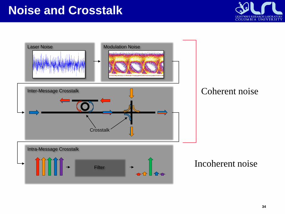
Noise and Crosstalk
Laser Noise
Inter-Message Crosstalk
Intra-Message Crosstalk
Modulation Noise
Crosstalk
Filter
Coherent noise
Incoherent noise
35
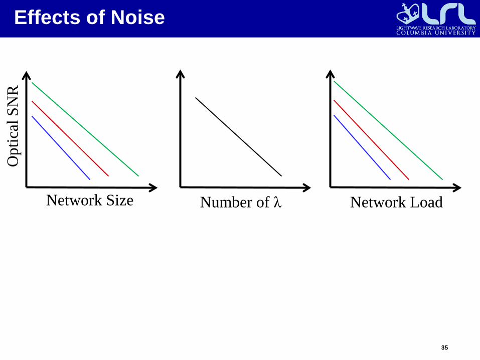
Effects of Noise
Network Size
Op
tical
SN
R
Number of λ Network Load

36
Simulation Results
0
10
20
30
40
50
Opt
ical
SN
R(d
B)
100 101 102 103 104 105 106 107
Message Size (bit)
TorusNon-blocking TorusTorusNXSquare Root
The line at OSNR=16.9 dB is where a bit-error-rate of 10-12 can be achieved, assuming an ideal binary receiver circuit and orthogonal signaling.
Results •Results are plotted for network size of 8×8 at saturation, at the detectors.• Maximum OSNR = ~45 dB (due to laser noise)• Minimum OSNR < 17 dB (due to message-to-message crosstalk)• Variations between networks due to varying likelihood of two message intersecting on network topology.
System Performance• SNR measures the likelihood of error-free transmission.• Lower SNR designs will require additional retransmission, resulting in lower throughput performance.

37
Photonic Plane Characteristics
• Insertion Loss• Noise• Power

38
Power Usage
0V1V
n-regionp-regionElectronic Control
0V
1V
OhmicHeater
Thermal Control
λ
Tran
sm
issio
n
Injected Wavelengths
Off-resonance profile
On-resonance profile
• Laser Power• Active Power
• Modulating• Detecting• Broadband
• Static Power• Thermal tuning
• Tx\Rx Power• Drivers• TIAs

39
Energy Per Bit
10-13
10-12
10-11
10-10
10-9
10-8E
nerg
ype
rB
it(J
/bit)
10-7
100 101 102 103 104 105 106 107
Message Size (bit)
TorusNon-blocking TorusTorusNXSquare Root

40
Power Breakdown
Router Logic43%
Router Buffer44%
Electronic Wire3%
Detector3%
Modulator4%
PSE2%
Thermal1%
Router Logic45%
Router Buffer44%
Electronic Wire2%
Detector2%
Modulator4%
PSE2%
Thermal1%
• Results based on randomly generated traffic with message sizes of 100 kbit, with network in saturation.• Data was collected on 64 nodes topologies constrained to a total surface area of 2 cm × 2 cm.
Torus Topology Nonblocking Torus Topology
• 7 wavelengths @ 10 Gbps/each• Power Dissipation = 1.59 W
• 12 wavelengths @ 10 Gbps/each• Power Dissipation = 4.31 W

41
Power Breakdown
Router Logic37%
Router Buffer31%
Electronic Wire1%
Detector10%
Modulator17%
PSE1%
Thermal3%
Router Logic34%
Router Buffer31%
Electronic Wire7%
Detector8%
Modulator14%
PSE2%
Thermal4%
Square Root Topology TorusNX Topology
• 38 wavelengths @ 10 Gbps/each• Power Dissipation = 3.22 W
• 27 wavelengths @ 10 Gbps/each• Power Dissipation = 1.89 W

Performance

43
Performance
• Uniform random traffic• 256 cores, 64-node network

44
Scientific Applications0.00001
0.0001
0.001
0.01
Cactus GTC MADbench PARATEC
Exe
cutio
n T
ime
(s) E-Mesh P-Mesh
0.00001
0.0001
0.001
0.01
0.1
Cactus GTC MADbench PARATEC
Ene
rgy
(J)
E-Mesh P-Mesh

Other Interesting Issues

46
Memory Access
Processor Core
Network Router
Memory Access Point
[G. Hendry et al. Circuit-Switched Memory Access in Photonic Interconnection Networks for HPEC. In Supercomputing, Nov. 2010]

47
Other Arbitration Means - TDM
[G. Hendry et al. Silicon Nanophotonic Network-On-Chip Using TDM Arbitration. In HOTI, Aug. 2010]

48
Wavelength Granularity
• Original Re-design
λ λ
Scalable number of WDM channels

49
Conclusion
• Some applications / programming models definitely well-suited to a circuit-switched photonic network
• Interesting tradeoffs and design space• Photonic physical layout / design• System-level benefits from device improvement• Network-level improvements