hybrid silicon / lithium niobate modulators: design …...hybrid silicon / lithium niobate...
TRANSCRIPT
Hybrid Silicon / Lithium Niobate Modulators:
Design and Wafer Bonding
TALI ILOVITSH
Submitted in partial fulfillment of the requirements for the Master's Degree
in the Faculty of Engineering, Bar-Ilan University
August 2012 Ramat-Gan, Israel

This research thesis was carried out under the supervision of
Dr. Avi Zadok from the Faculty of Engineering at Bar-Ilan
University

Acknowledgements
This Thesis would not have been possible without the guidance and the help of several individuals who in one way or another contributed and extended their valuable assistance in the preparation and completion of this study. First and foremost I offer my utmost gratitude to my supervisor, Dr. Avi Zadok, who has supported me throughout my thesis with his patience, knowledge and encouragement . Prof. Chaim Sukenik from the Department of Chemistry and his students – Vlada Artel and Moran Shubely, for their major contribution in the chemical processes and allowing the usage of their clean room . Idan Bakish, my colleague, who worked alongside me in the clean room, assisted me in samples preparation and was a full companionship throughout the research work. My fellow students in Dr. Avi Zadok's group, for creating a friendly and cheerful environment to work in: Ofir Klinger, Yonatan Stern, Raphael Cohen, Yair Antman, Ran Califa, Shahar Levy, Eyal Preter, Daniel Kravitz, Daniel Grodensky, Alon Lehrer, David Elooz, and Dr. Arkady Rudnitsky Prof. Shlomo Ruschin from the Department of Electrical Engineering, Tel Aviv University for the valuable insights he has shared. Eyal Shekel from Civan Advanced Technologies Ltd., who assist me in overcoming obstacles throughout this research work, and provided us with LiNbO3 samples . Dina Yemini, the administrator of the Faculty of Engineering Bar Ilan University, for assisting me whenever needed and for encouraging me to pursue professional growth. The Faculty of Engineering, Bar Ilan University, that has provided the support and equipment I have needed to produce and complete my thesis and for providing me a scholarship that allowed me to complete my studies. The Bar-Ilan Institute of Nanotechnology and Advanced Materials (BINA), for providing my fellowship, and providing the access to fabrication and characterization instrumentation. Finally, I would like to thank my beloved husband, Asaf, for his companionship, his constant support and useful advices . Last but not least, I want to show my gratitude to my family, and especially my mother and father, for their readiness to give me the time to concentrate on this research. Thank you for your care, and for teaching me to strive for the best.


i
Table of contents
TABLE OF CONTENTS ............................................................................................................................... I
TABLE OF FIGURES ................................................................................................................................. III
GLOSSARY OF ACRONYMS ....................................................................................................................VI
LIST OF PUBLICATIONS ....................................................................................................................... VIII
ABSTRACT ............................................................................................................................................... 1
1. INTRODUCTION ...................................................................................................................... 4
1.1 THEORETICAL BACKGROUND .................................................................................................. 5
1.1.1 Why Silicon photonics? ............................................................................................ 5
1.1.2 Passive devices in Silicon .......................................................................................... 8
1.1.3 Active devices in Silicon ......................................................................................... 10
2. ELECTRO OPTIC MODULATORS (EOM) .................................................................................. 11
2.1 MODULATION PRINCIPLES .................................................................................................... 11
2.2 LINEAR ELECTRO-OPTIC EFFECT (POCKELS EFFECT) ....................................................................... 12
2.3 SILICON MODULATORS ....................................................................................................... 13
2.4 HYBRID SILICON/INP MODULATORS ........................................................................................ 16
2.5 HYBRID SILICON/LINBO3 MODULATORS ................................................................................... 18
2.5.1 Bonding techniques for use in silicon photonics ....................................................... 20
2.5.2 Reported attempts for bonding silicon and LiNbO3 ................................................... 21
3. DEVICE DESIGN .................................................................................................................... 26
3.1 DEVICE STRUCTURE ............................................................................................................ 26
3.2 HYBRID WAVEGUIDE DESIGN ................................................................................................. 27
3.2.1 Modulator operation voltage and length calculation ............................................... 31
3.2.2 Waveguide dimensions .......................................................................................... 36
3.2.3 Operation voltage and length results ...................................................................... 38
4. WAFER BONDING USING SELF-ASSEMBLED MONOLAYERS ..................................................... 42
4.1 BONDING BETWEEN SILICON AND LINBO3 ................................................................................. 42
4.2 SELF-ASSEMBLED MONOLAYER (SAM) ................................................................................... 43
4.3 WAFER BONDING PROCEDURE, BASED ON SELF-ASSEMBLED MONOLAYERS ......................................... 46

ii
4.4 SURFACE ANALYSIS ............................................................................................................. 51
4.5 BONDING INTERFACE CHARACTERIZATION ................................................................................. 56
5. CHARACTERIZATION OF DEPOSITED MONOLAYERS AND SUBSEQUENT BONDING ....... 60
5.1 MONOLAYER DEPOSITION .................................................................................................... 60
5.1.1 Octadecyltrichlorosilane(OTS) terminated SAM ...................................................... 60
5.1.2 Thioacetate (TA) terminated SAM ......................................................................... 62
5.2 THIOLS-FORMING HYDROLYSIS ............................................................................................... 64
5.3 CONVERSION OF THIOLS TO DISULFIDES .................................................................................... 66
5.4 WAFER BONDING ATTEMPTS BASED ON DISULFIDE EXCHANGE REACTION ............................................ 66
5.5 ALTERNATIVE BONDING PROCEDURE: THIOLS-TO-PLATINUM .......................................................... 70
6. SUMMERY AND CONCLUSIONS ............................................................................................. 72
REFERENCES ......................................................................................................................................................... 74
iii
Table of figures
Figure 1.1 Heat generation per unit area within micro-processor chip, as a function of decreasing
device feature size [15]. .......................................................................................................................... 6
Figure 1.2 The linear absorption spectrum of silicon [16]. ..................................................................... 7
Figure 1.3 left – top view of a directional coupler, consisted of two waveguides. The waveguides are
in close proximity over a certain region. Right – transverse cross-section of the refractive index
geometry of the two waveguides in proximity, and are the refractive indexes of the two
waveguides, is the refractive index of the volume in which the two waveguides are places [21]. .. 8
Figure 1.4 Schematic illustration of a Mach-Zender interferometer [21] .............................................. 9
Figure 1.5 Left – Schematic illustration of a ring resonator. Right – several examples of fabricated
micro-ring resonators on silicon [22]. ..................................................................................................... 9
Figure 2.1 Schematic illustration of a Mach-Zender interferometer electro-optic modulator ............ 12
Figure 2.2 A ring-resonator electro-optic modulator in silicon. The transmission of the modulator is
modified by the electrical injection of carriers to the ring waveguide, which spans a p-n junction.
Right – schematic illustration. Left – fabricated device before and after the deposition of electrodes
[32] . ...................................................................................................................................................... 14
Figure 2.3 A scanning electron microscope image of silicon rib waveguide at a p-n junction (left), and
the junction I-V characteristics (right). Right inset: a schematic illustration of MZI modulator that is
based on carrier injection into the junction[33]. .................................................................................. 15
Figure 2.4 Cross-sectional diagram of a high-bandwidth, all-silicon phase modulator [34] ................ 16
Figure 2.5 Detailed structure of the III–V epitaxial stack and the SOI wafer [38] ................................ 17
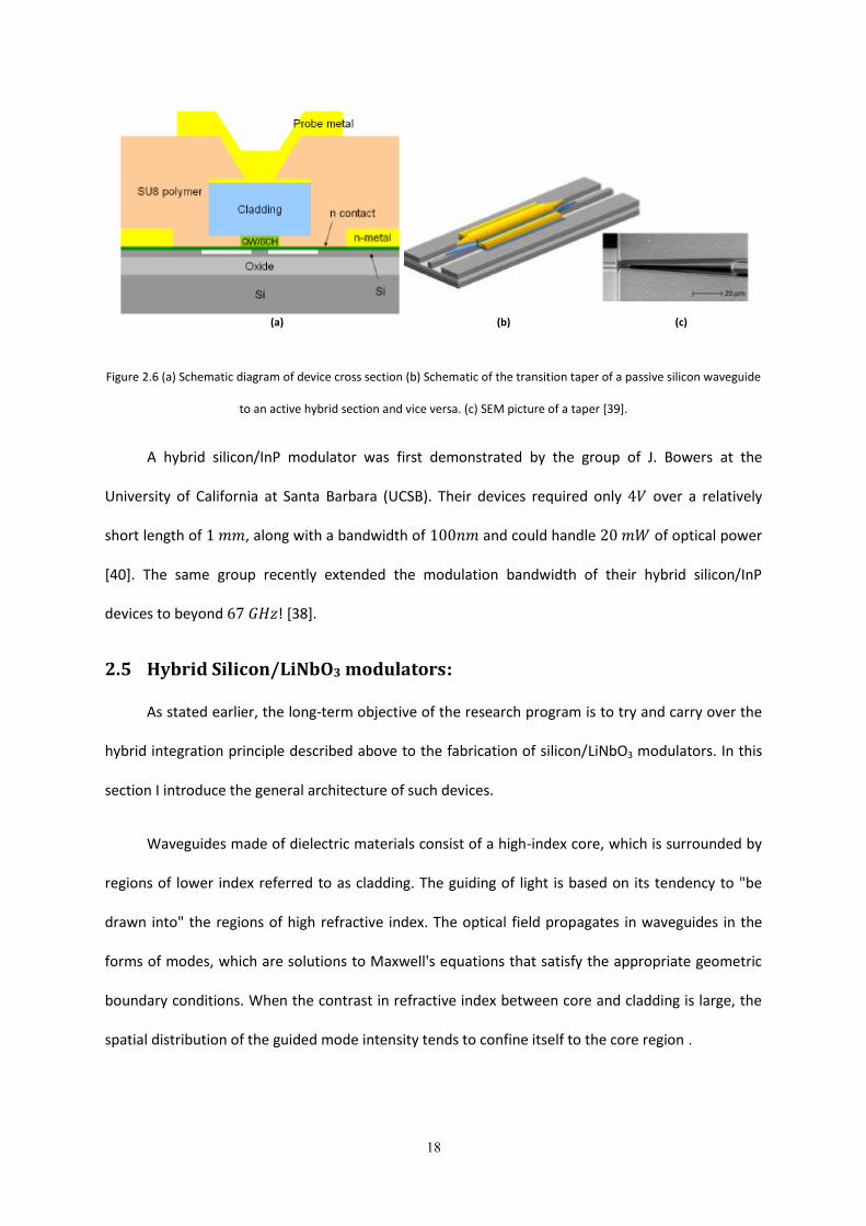
Figure 2.6 (a) Schematic diagram of device cross section (b) Schematic of the transition taper of a
passive silicon waveguide to an active hybrid section and vice versa. (c) SEM picture of a taper [39].
.............................................................................................................................................................. 18
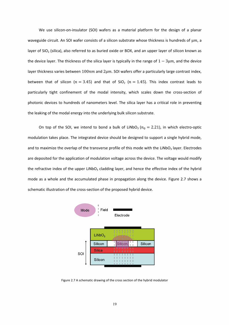
Figure 2.7 A schematic drawing of the cross section of the hybrid modulator .................................... 19
Figure 2.8 Transmission electron image of the extracted lamella. From bottom to top the layers are
silicon, the bonded silver layer, Lithium Niobate, and the protective platinum layer[9]. .................... 22
Figure 2.9 Infrared transmission image of Si/ LiNbO3 bonded by the modified SAB process at room
temperature[11]. .................................................................................................................................. 22
Figure 2.10 The procedure for obtaining single crystal LiNbO3 micro-platelets and transferring and
integrating them on Si-on-insulator substrate[10]. .............................................................................. 24
Figure 2.11 The integration procedure for the hybrid structure LiNbO3 micro-platelet and silicon
micro-ring waveguide[10]. .................................................................................................................... 24
Figure 3.1 Potential geometries of hybrid silicon / LiNbO3 electro-optic modulators. ........................ 26
Figure 3.2 Schematic drawing of the hybrid waveguide device cross-section. The waveguide consists
of a guiding Si layer of thickness d with a refractive index n2, surrounded by LiNbO3 and Silica medias
of refractive index n1 and n3 respectively ............................................................................................. 27
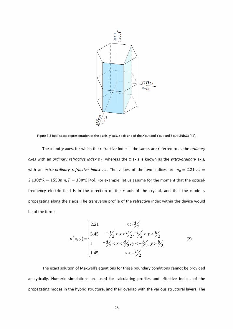
Figure 3.3 Real-space representation of the x axis, y axis, z axis and of the X cut and Y cut and Z cut
LiNbO3 [44]. .......................................................................................................................................... 28
Figure 3.4 illustration of one-dimensional asymmetric slab waveguide .............................................. 30
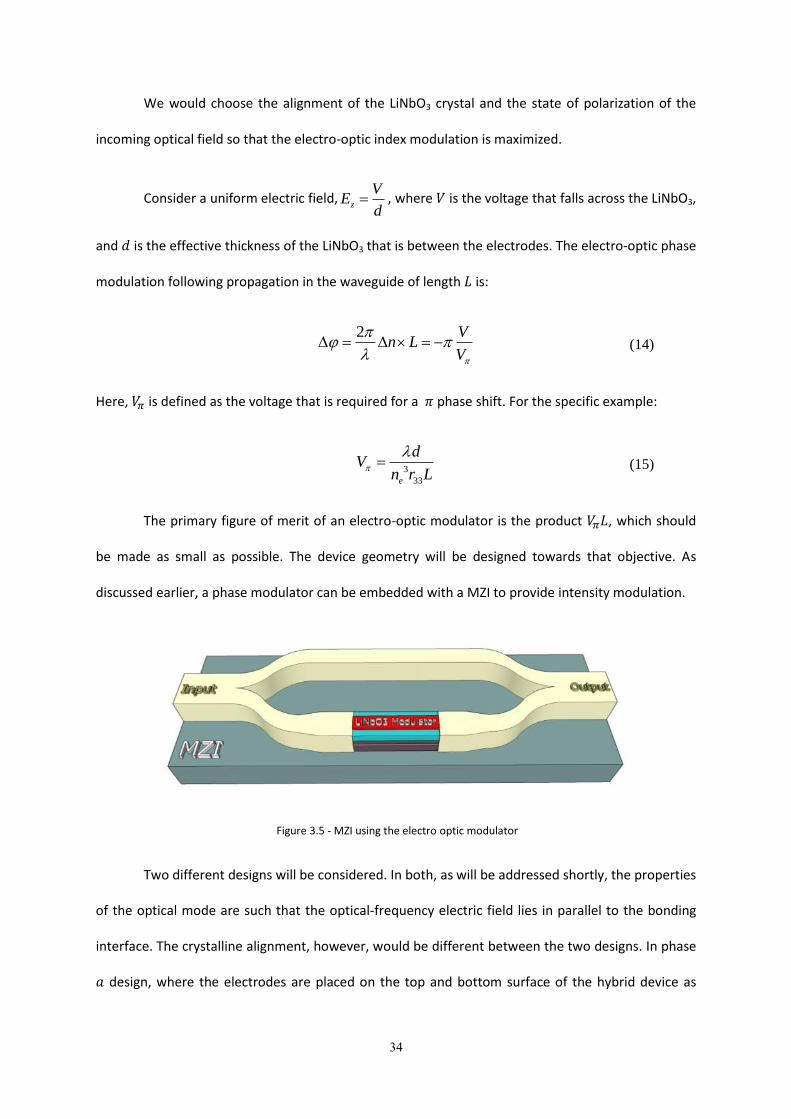
Figure 3.5 - MZI using the electro optic modulator .............................................................................. 34
iv
Figure 3.6 – Applied voltage and electrodes orientation of the modulator. The orientation of the axes
in both panels relate to the crystalline axes of LiNbO3. ........................................................................ 35
Figure 3.7 – Transverse profiels of electric field components. left, middle,
right ............................................................................................................................. 36
Figure 3.8 – Transverse profiels of magnetic field components. left,
middle, right ............................................................................................................... 37
Figure 3.9 - Calculated two dimensional electric field strength ( ) mode profiles with different
silicon waveguide width of (a) 0.4 μm, (b) 0.45μm, (c) 0.5 μm and (d) 0.6 μm. The silicon waveguide
height is fixed at 0.22 μm...................................................................................................................... 37
Figure 3.10 - Calculated confinement factors and effective index of the fundamental TM mode with
different silicon waveguide widths. ...................................................................................................... 38
Figure 3.11 - Calculated two dimensional electric field strength ( ) mode profile of the second
mode, with silicon waveguide width of 1 μm and height of 0.22 μm .................................................. 38
Figure 3.12 – Simulated external electric field through the device in the large electrode spacing
configuration ......................................................................................................................................... 39
Figure 3.13 – Comsol simulations of the voltage and electric field through the device in the close
electrode spacing configuration. The colors present the voltage and the arrows show the electric
field directions ...................................................................................................................................... 41
Figure 4.1 molecule structure of Trichlorosilane (SiCl3). ...................................................................... 44
Figure 4.2 Molecular structure of Octadecyl-trichloro-silane(OTS). ..................................................... 45
Figure 4.3 Structure of the monolayer-forming molecule, with thioacetate group on the other end. 46
Figure 4.4 Monolayer molecule (left) and assembly process (right). ................................................... 48
Figure 4.5 Illustration of the hydrolysis reaction for cleaving the free-standing thioacetate end-group
of self-assembled monolayers, leaving a thiol-decorated surface. ...................................................... 49
Figure 4.6 A reaction for converting Thiol terminating groups to disulphide groups. ......................... 50
Figure 4.7 The bonding press closed (left) and the bonding press open (right). .................................. 50
Figure 4.8 Illustration of a wafer bonding process, based on a disulphide exchange reaction among
monolayers on both surfaces. .............................................................................................................. 51
Figure 4.9 Contact angle measurement of a water droplet on an untreated Silicon surface (left) and
on an OTS-coated Silicon surface (right). .............................................................................................. 53
Figure 4.10 Schematic illustration of an ATR-FTIR measurement of thin organic films ....................... 53
Figure 4.11 schematic drawing of Ellipsometry measurement ............................................................ 54
Figure 4.12 Schematic view of Air/Film/Substrate Ellipsometry experiment ....................................... 55
Figure 4.13 Schematic infrared transmission microscopy setup. ......................................................... 57
Figure 4.14 schematic drawing of the electron and x-ray optics of a SEM........................................... 58
Figure 4.15 Pull-off adhesion test equipment ...................................................................................... 59
Figure 5.1 Infra-red absorption spectra of OTS coated Silicon (top) and LiNbO3 (bottom) sample . .. 61
Figure 5.2 a water droplet on an untreated surface of both Si (a) and LiNbO3 (c) and on OTS coated Si
(b) and LiNbO3 (d) ................................................................................................................................. 62
Figure 5.3 Infra-red absorption spectra of TA coated silicon sample. .................................................. 63
Figure 5.4 a water droplet on TA coated Si (a) and LiNbO3 (b) ............................................................. 63
Figure 5.5 Infra-red absorption spectra of a monolayer-coated silicon sample. Following deposition
(red) and following successful hydrolysis (blue). .................................................................................. 64
Figure 5.6 a droplet of water on a TA coated Si before (a) and after (b) hydrolysis ............................ 65

v
Figure 5.7 a droplet of water on a TA coated LiNbO3 before (a) and after (b) hydrolysis. Striping of the
monolayer is evident after hydrolysis. .................................................................................................. 65
Figure 5.8 a droplet of water on a TA coated on LiNbO3 surface that was pre-deposited by a 20 nm-
thick layer of silica before (left) and after (right) hydrolysis ................................................................ 66
Figure 5.9 A sample of two bonded silicon pieces (~ 1 X 1 cm2)........................................................... 67
Figure 5.10 A sample of Si and LiNbO3 bonded pieces using Silica as a mediated layer ..................... 68
Figure 5.11 SEM image of the interface of Si bonded to InP ................................................................ 69
Figure 5.12 (a) Bonded InP and silicon samples. (b) Infra-red microscopy image of an InP sample and
a silicon sample bonded together. Rings appear in a corner region that was taken from the edge of
the InP wafer and could not be bonded. An illustration of the partially bonded samples is shown
above the microscopy image. IR image of the interface of Silicon bonded to InP ............................... 70
Figure 5.13 A sample of Si and LiNbO3 bonded pieces using platinum as a mediated layer. .............. 71

vi
Glossary of Acronyms
AFM Atomic force microscopy
Ar Argon
ATR Attenuated total reflection
BCB Benzocyclobutene
CMOS Complementary metal oxide semiconductor
CO2 Carbon dioxide
CTE Coefficient of thermal expansion
CVD Chemical vapor deposition
CW continuous wave
DI Deionized
DNFB Dinitrofluorobenzene
EAM Electro absorption modulator
EOM Electro optic modulator
FCI Free-carrier index change effect
FTIR Fourier transform infrared spectroscopy
FWM Four-wave mixing
GaAs Gallium-Arsenide
H Hydrogen
H2O2 Hydrogen peroxide
H2SO4 Sulfuric acid
HCL Hydrochloric acid
He Helium
HF Hydrofluoric acid
IC integrated circuits
vii
IIR Infinite impulse response
InP Indium Phosphide
IR Infrared
LED Light-emitting diode
LiNbO3 Lithium Niobate
MQW Multiple quantum well
MZI Mach-Zehnder interferometer
OTS Octadecyl-trichloro-silane
QCSE Quantum-confined Stark effect
QW Quantum well
SAM Scanning acoustic microscopy
SAM Self-assembled monolayers
SEM Scanning electron microscope
Si silicon
SiCl3 Trichlorosilane
SiO2 Silica
SOA Semiconductor optical amplifier
SOI Silicon on insulator
SPM Self-phase modulation
SRS Stimulated Raman scattering
TA Thioacetate
TE Transverse Electric
TM Transverse Magnetic
V volt
XPM Cross-phase modulation
viii
List of publications
Journal Publications:
I. Bakish, V. Artel, T. Ilovitsh, M. Shubely, Y. Ben-Ezra, A. Zadok and C. N. Sukenik, "Self-assembled monolayer assisted bonding of Si and InP", Optical Materials Express, 2, 1141-1148 (2012) .
Refereed proceedings publications:
V. Artel, I. Bakish, T. Ilovitsh, M. Shubely, A. Zadok, and C. N. Sukenik "Organic Self-Assembled Monolayers as a Tool for Low Temperature Wafer Bonding", 4th Congress of the European Association for Chemical and Molecular Sciences (EuCheMS) Chemistry Congress, Prague, Czech Republic, (August 2012).
I. Bakish, T. Ilovitsh, V. Artel, M. Shubely, A. Zadok and C. N. Sukenik, "Low Temperature Wafer Bonding of Silicon to InP and Silicon to LiNbO3 Using Self-Assembled Monolayers", Optical Fiber Communication (OFC) conference, Convention center, LA (March 2012).
V. Artel, T. Ilovitsh, I. Bakish, M. Shubely, E. Shekel, Y. Ben-Ezra, C. N. Sukenik, and A. Zadok, “Wafer bonding techniques for hybrid silicon photonic devices based on surface modifications,” proceedings of the 14th Transparent Optical Networks (ICTON), Coventry, UK, July 2011.
Non-refereed presentations:
T. Ilovitsh, I. Bakish, V. Artel, M. Shubely, Y. Ben-Ezra, E. Shekel, S. Zach, A. Zadok and C. N. Sukenik ,"Low Temperature Wafer Bonding of Silicon to InP and Silicon to LiNbO3 Using Self-Assembled Monolayers", NanoIsrael 3rd conference, David Intercontinental hotel, Tel Aviv (March 2012).
I. Bakish, T. Kraus, V. Artel, M. Shubely, Y. Ben-Ezra, E. Shekel, S. Zach, A. Zadok and C. N. Sukenik ,"Low Temperature Wafer Bonding of Silicon to InP and Silicon to LiNbO3 Using Self-Assembled Monolayers", BINA conference, Na Laga'at center, Jaffa port, Tel Aviv (October 2011).

1
Abstract
Optical communication has provided the exclusive means for carrying high capacity data
over long distances for over three decades. As modern data storage and computing rely increasingly
on high-rate sharing of information, optics-based techniques steadily penetrate towards rack-level,
board-level and even chip-level communications. The future growth of both computation and
communication depends, to a large extent, on the successful integration of optical communication
system functionalities alongside electronic integrated circuits on the silicon material platform.
Hence, the realization of photonic devices on silicon, or silicon photonics, is a research area of much
interest and significance.
While the silicon-on-insulator (SOI) material platform is generally favorable for making
passive devices such as waveguides, interferometers and resonators, the properties of silicon raise
several challenges to the implementation of active photonic devices such as electro-optic
modulators and light sources. The state-of-the-art silicon-photonic light sources, amplifiers,
modulators and detectors rely on the hybrid integration of additional electro-optic materials, most
often InP-based semiconductors, on top of SOI waveguides. One material drawback of silicon is the
absence of a second-order electro-optic effect. This effect is responsible for the change in refractive
index through the application of external voltage, and is at the basis of electro-optic modulators,
which are key components in optical communication networks. The most widely used material in
electro-optic modulators is LiNbO3. LiNbO3 has a high electro optic coefficient, and the fabrication
technology of LiNbO3-based devices is mature and well established. The hybrid integration of LiNBO3
alongside silicon in a single device is therefore of much interest and potential significance.
The work presented herein is part of a long-term research program, aiming to realize hybrid
electro-optic modulators in LiNbO3 over SOI. More specifically, the work addresses two main
2
challenges associated with that objective: the bonding of LiNbO3 to silicon, and the design of the
hybrid waveguide structure
The most commonly-used technique for bonding dissimilar electro-optic materials is direct
bonding. Direct bonding is carried out without any additional intermediate layers. When clean and
activated, mirror-polished, flat surfaces are put together subject to pressure and heat hydrogen
bonds can initially form across the two surfaces. Following annealing at comparatively high
temperatures of , the hydrogen may be released and covalent bonds may form
instead. Although this method is successfully employed, for example, in the fabrication of hybrid
silicon-InP electro-optic devices, it is not applicable for the bonding of silicon and LiNbO3 due to the
mismatch in thermal expansion coefficients between the two materials. Another bonding method
relies on the application of relatively thick intermediate adhesive layer. However, the adhesive could
disrupt the coupling of light between the two media. Correspondingly, there are only a few reports
of bonding LiNbO3 to Silicon in the literature.
A large part of the work is dedicated to a new bonding paradigm, which relies on the
deposition of self-assembled monolayers (SAMs) of specially-synthesized organic materials on both
surfaces and their subsequent functionalization using chemical reactions. The SAMs modify the
surface properties of the two materials in ways that permit their subsequent bonding at low
temperatures. The wafer bonding procedure and its monitoring and analysis are described in detail.
The advantage of this method is the use of a relatively low temperature of 120⁰C. Low bonding
temperatures reduce the excessive thermal stresses across the bonding interface. The monolayer-
based processed was successfully applied to the bonding of two silicon samples to one another.
On the design parts, two geometries are considered. First, a design with large electrodes
spacing, on the order of hundreds of microns, is proposed and analyzed. This design is simpler to
fabricate, but the large spacing restricts its potential operation of high voltages and low rates.
Second, a more advanced device with closely spaced electrodes is also designed. Our analysis and

3
simulations suggest that hybrid silicon-LiNbO3 modulators should be feasible, with a product
that is on the same order of magnitude as that of stand-alone LiNbO3 modulators.
The final part of this thesis will discuss the bonding results. Despite several successes, the
bonding of silicon to LiNbO3 faced difficulties and most of the attempts did not result in actual
bonding, and only showed handling strength. We attribute these difficulties primarily to unfavorable
preparation conditions. Potential solution paths for bonding improvements are discussed in the
summarizing section. I hope that with certain modifications in place for the bonding process, hybrid
LiNbO3 / silicon electro-optic modulators could be realized.

4
1. Introduction
Silicon photonics is a research subject dedicated to the implementation of electro-optic
devices on the silicon material platform[1]. The field is of great significance, due to the promise of
monolithic integration of electro-optic devices with silicon electronics [2]. However, silicon suffers
from a few drawbacks from optical devices perspective. One such drawback is the absence of a
second-order electro-optic effect [3]. This effect is responsible for the change in refractive index
through the application of external voltage [4]. The effect is at the basis of electro-optic modulators,
which are key components in optical communication networks. The most widely used material in
electro-optic modulators is LiNbO3. The electro optic coefficient of LiNbO3 is a high:
⁄ , and
the fabrication technology of LiNbO3 based devices is mature and well established [5].
The hybrid integration of LiNbO3 alongside silicon in a single device is therefore of much
interest and potential significance. One possible solution path towards silicon-photonic modulators
relies on the hybrid integration of additional electro-optic materials, in our case LiNbO3, on top of
silicon waveguides. The main method used for bonding dissimilar electro-optic materials is direct
bonding. Direct bonding is carried out without any additional intermediate layers. When clean and
activated, mirror polished, flat surfaces are put one on top of the other under pressure and heat,
hydrogen bonds can initially form across the two surfaces. Following annealing at high temperatures
between , the hydrogen may be released and covalent bonds may form instead.
Although this method is successfully employed, for example, in the fabrication of hybrid silicon-InP
electro-optic devices [6,7], only few reports of bonding silicon to LiNbO3 appear in the literature[8–
13]. The bonding of LiNbO3 and Silicon is particularly challenging, due to the mismatch in the
coefficients of thermal expansion (CTEs) between Silicon and LiNbO3. The mismatch is in the range
of – at room temperature and depends on the orientation of LiNbO3: The CTE values are
⁄ for Silicon,
⁄ for X-cut LiNbO3 and
⁄ for Z-cut LiNbO3 at [14]. These CTE
5
levels do not allow for direct wafer bonding at high temperatures due to thermal stresses across the
interface.
The thesis focuses on two critical aspects of the silicon / LiNbO3 hybrid technology: the
bonding between the two surfaces, and the design and simulation of the hybrid waveguide
geometry, as well as the propagation of light in the combined structure.
1.1 Theoretical background:
1.1.1 Why Silicon photonics?
The main driving force behind the modern silicon photonics research is that of optical inter-
connects among computer boards, among processor chips and even within a single chip. For nearly a
decade already, the operating speed of micro-electronic devices is no longer restricted by the
switching time of transistor gates themselves, but rather by the delay associated with the electrical
wiring inside the processor chip. Every squared centimeter of chip area has an estimated wiring
length of ! The complexity that is associated with such wiring length is immense. Even as early
as , processor chips had six different metallic layers. Nowadays they have even more. The
reduction in dimensions and increase in density of electrical wiring give rise to a plethora of issues,
such as prolonged latency and crosstalk among devices. Optical interconnect might, at least in
principle, alleviate such problems.
6
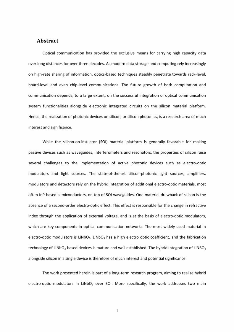
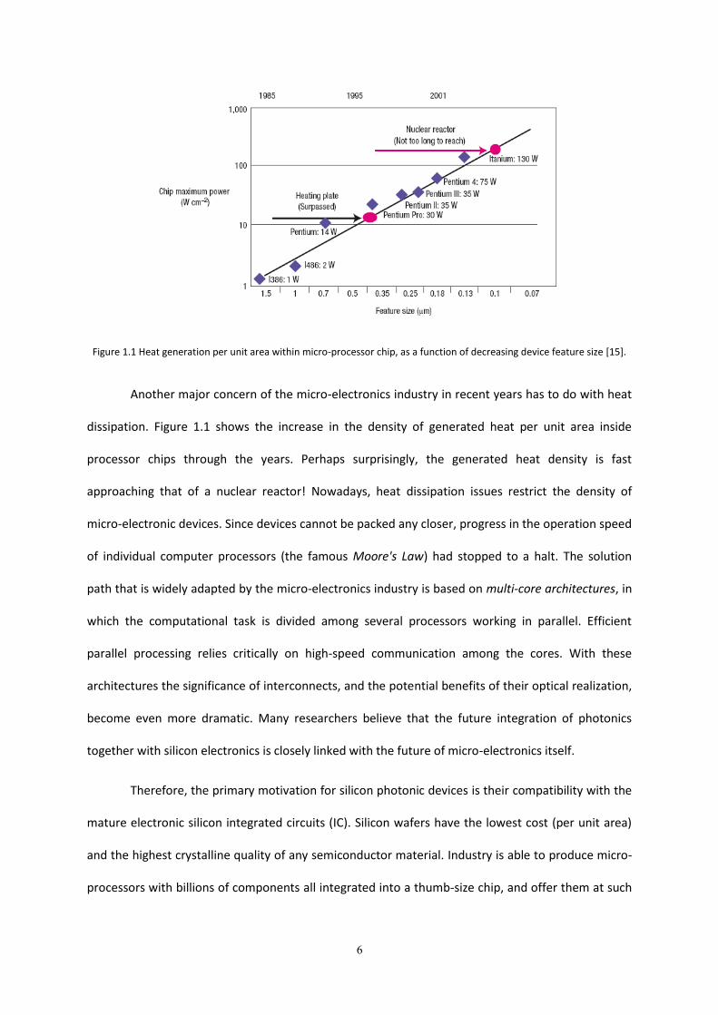
Figure 1.1 Heat generation per unit area within micro-processor chip, as a function of decreasing device feature size [15].
Another major concern of the micro-electronics industry in recent years has to do with heat
dissipation. Figure 1.1 shows the increase in the density of generated heat per unit area inside
processor chips through the years. Perhaps surprisingly, the generated heat density is fast
approaching that of a nuclear reactor! Nowadays, heat dissipation issues restrict the density of
micro-electronic devices. Since devices cannot be packed any closer, progress in the operation speed
of individual computer processors (the famous Moore's Law) had stopped to a halt. The solution
path that is widely adapted by the micro-electronics industry is based on multi-core architectures, in
which the computational task is divided among several processors working in parallel. Efficient
parallel processing relies critically on high-speed communication among the cores. With these
architectures the significance of interconnects, and the potential benefits of their optical realization,
become even more dramatic. Many researchers believe that the future integration of photonics
together with silicon electronics is closely linked with the future of micro-electronics itself.
Therefore, the primary motivation for silicon photonic devices is their compatibility with the
mature electronic silicon integrated circuits (IC). Silicon wafers have the lowest cost (per unit area)
and the highest crystalline quality of any semiconductor material. Industry is able to produce micro-
processors with billions of components all integrated into a thumb-size chip, and offer them at such
7
a low price that they appear in consumer electronics. Creating low-cost photonics for the mass
market applications by exploiting the IC industry is a major motivation for silicon photonics.
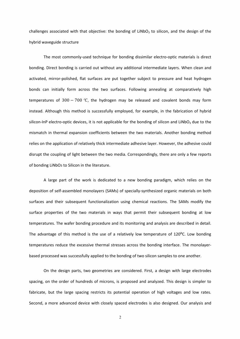
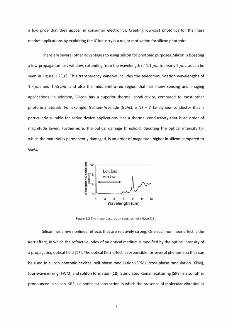
There are several other advantages to using silicon for photonic purposes. Silicon is boasting
a low-propagation-loss window, extending from the wavelength of to nearly , as can be
seen in Figure 1.2[16]. This transparency window includes the telecommunication wavelengths of
and , and also the middle-infra-red region that has many sensing and imaging
applications. In addition, Silicon has a superior thermal conductivity, compared to most other
photonic materials. For example, Gallium-Arsenide (GaAs), a family semiconductor that is
particularly suitable for active device applications, has a thermal conductivity that is an order of
magnitude lower. Furthermore, the optical damage threshold, denoting the optical intensity for
which the material is permanently damaged, is an order of magnitude higher in silicon compared to
GaAs.
Figure 1.2 The linear absorption spectrum of silicon [16].
Silicon has a few nonlinear effects that are relatively strong. One such nonlinear effect is the
Kerr effect, in which the refractive index of an optical medium is modified by the optical intensity of
a propagating optical field [17]. The optical Kerr effect is responsible for several phenomena that can
be used in silicon photonic devices: self-phase modulation (SPM), cross-phase modulation (XPM),
four-wave mixing (FWM) and soliton formation [18]. Stimulated Raman scattering (SRS) is also rather
pronounced in silicon. SRS is a nonlinear interaction in which the presence of molecular vibration at
8
THz frequencies ("optical phonons") modifies the effective refractive index of the optical medium
and couples between light waves of different frequencies [19].
1.1.2 Passive devices in Silicon
By passive devices we refer to the routing of light in waveguide paths from one point on a
photonic chip to another. Waveguide paths may split and combine to form filters, and even close
into rings that provide feedback loops, also referred to as resonator structures. Devices in which
light undergoes absorption and attenuation at particular locations or wavelengths also qualify as
passive. Passive silicon-photonic devices are highly compact, provide low losses, withstand high
intensities, and may operate in a broad range of wavelengths. In the following I briefly introduce
three examples of passive photonic devices that are commonly realized in silicon:
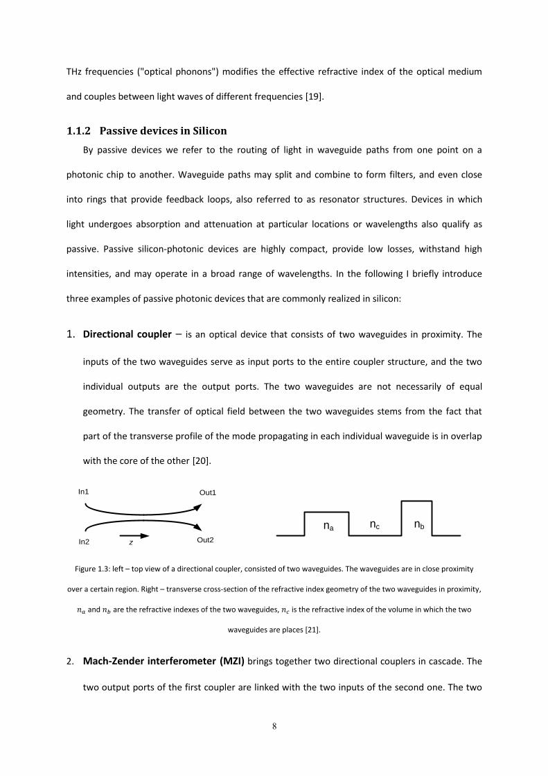
1. Directional coupler – is an optical device that consists of two waveguides in proximity. The
inputs of the two waveguides serve as input ports to the entire coupler structure, and the two
individual outputs are the output ports. The two waveguides are not necessarily of equal
geometry. The transfer of optical field between the two waveguides stems from the fact that
part of the transverse profile of the mode propagating in each individual waveguide is in overlap
with the core of the other [20].
In1
In2
Out1
Out2z
na nbnc
ncna nb
In1
In2
Out1
Out2z
na nbnc
ncna nb
Figure 1.3: left – top view of a directional coupler, consisted of two waveguides. The waveguides are in close proximity
over a certain region. Right – transverse cross-section of the refractive index geometry of the two waveguides in proximity,
and are the refractive indexes of the two waveguides, is the refractive index of the volume in which the two
waveguides are places [21].
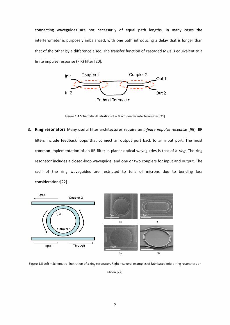
2. Mach-Zender interferometer (MZI) brings together two directional couplers in cascade. The
two output ports of the first coupler are linked with the two inputs of the second one. The two
9
connecting waveguides are not necessarily of equal path lengths. In many cases the
interferometer is purposely imbalanced, with one path introducing a delay that is longer than
that of the other by a difference sec. The transfer function of cascaded MZIs is equivalent to a
finite impulse response (FIR) filter [20].
Figure 1.4 Schematic illustration of a Mach-Zender interferometer [21]
3. Ring resonators Many useful filter architectures require an infinite impulse response (IIR). IIR
filters include feedback loops that connect an output port back to an input port. The most
common implementation of an IIR filter in planar optical waveguides is that of a ring. The ring
resonator includes a closed-loop waveguide, and one or two couplers for input and output. The
radii of the ring waveguides are restricted to tens of microns due to bending loss
considerations[22].
Figure 1.5 Left – Schematic illustration of a ring resonator. Right – several examples of fabricated micro-ring resonators on
silicon [22].
11
1.1.3 Active devices in Silicon
The role of silicon is more complex in active photonic devices. These include critical
components such as light sources in the forms of light-emitting diodes (LEDs) and laser diodes,
semiconductor optical amplifiers (SOAs), electro-optic modulators which imprint information upon a
continuous optical field, and detectors. Silicon suffers from fundamental drawbacks which keep it
from realizing few of these functionalities in a straight-forward manner. For example, the indirect
semiconductor band gap of silicon makes it a poor converter of electrical current to light, a
deficiency which makes the realization of silicon light sources very challenging. Also, the electro-
optic effect which underlies the operation of modulators in several other materials is practically
absent in silicon. Therefore, integration of additional materials is often needed to realize active
devices on silicon. In the next section we focus on modulators, which are the objectives of this work.
11
2. Electro Optic modulators (EOM):
An electro-optic modulator (EOM) is a device which uses an electrical input waveform to modify
the amplitude and / or phase of an incoming light wave. The role of an electro-optic modulator in a
communication system is to super-impose data, which exists in the electrical domain, onto a
continuous wave (CW) optical carrier.
2.1 Modulation Principles
In traditional optical communication, the data is carried as binary on/off keying of the optical
amplitude: a logical ' ' is represented by some level P of the optical power, whereas a logical ' ' is
represented by transmitting (ideally) no power. There are two ways to obtain amplitude modulation:
The first is direct modulation, in which the current driving a laser diode light source is being
modified. The advantage in this method is that it doesn't require additional components. However, it
imposes severe restrictions upon the modulation rate, and introduces parasitic frequency
modulation (referred to as 'chirp')[23]. The second method is known as external light modulation, in
which an additional component modifies the amplitude of a laser source which is operated in
continuous-wave mode.
Two types of external modulators are widely used commercially:
a) Electro-absorption modulators (EAMs) [24], which directly modify the amplitude of a
propagating optical wave. Its principle of operation is based on the Franz-Keldysh effect [25]: an
applied electric field changes the bandgap energy, which in turn modifies the absorption
spectrum. EAMs make use of a waveguide that is made with a semiconductor material whose
bandgap is slightly higher than the energy of incoming photons. Therefore, the material is
nominally transparent. However, the material bandgap can become smaller with the application
of an external voltage, making the material highly absorptive.
12
Many EAMs make use of multiple quantum wells (MQWs): thin layers of low-bandgap
semiconductor which lie in between barriers of higher bandgap. The spatial confinement leads
for discretization of the electron and hole energy levels in the structure. Absorption in MQW is
typically stronger than in bulk semiconductor media [26], due to the spatial overlap between
the electron and hole wave functions. EAMs in MQWs make use of the quantum-confined Stark
effect (QCSE) [27]: an external electric field pulls electrons and holes in opposite directions,
thereby reducing their spatial overlap and the absorption efficiency. EAM is effective for photon
energies slightly below the medium bandgap. The bandgap of silicon, which corresponds to a
wavelength of approximately , is far larger than the energy of photons at the
telecommunication wavelength of . Therefore, the effect is inadequate for use in
silicon modulators.
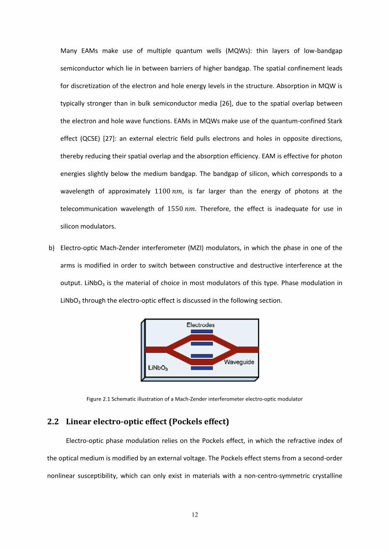
b) Electro-optic Mach-Zender interferometer (MZI) modulators, in which the phase in one of the
arms is modified in order to switch between constructive and destructive interference at the
output. LiNbO3 is the material of choice in most modulators of this type. Phase modulation in
LiNbO3 through the electro-optic effect is discussed in the following section.
Figure 2.1 Schematic illustration of a Mach-Zender interferometer electro-optic modulator
2.2 Linear electro-optic effect (Pockels effect)
Electro-optic phase modulation relies on the Pockels effect, in which the refractive index of
the optical medium is modified by an external voltage. The Pockels effect stems from a second-order
nonlinear susceptibility, which can only exist in materials with a non-centro-symmetric crystalline
13
structure [28]. Silicon, whose crystalline arrangement possesses a center of symmetry, does not
support this effect.
The Pockels effect is particularly pronounced in LiNbO3. The extent of refractive index change
in a LiNbO3 crystal depends on the relative orientations of the external field, the electric field vector
of the optical-frequency wave, and the orientation of the crystal. Different arrangements will be
addressed in detail later. An order of magnitude estimate can be obtained as follows. Subject to an
external voltage , the electro-optic change in refractive index is given by [29]:
, (1)
where d is the distance between the electrodes surrounding the crystal, is the
refractive index for linear propagation, and its numeric value would depend on the polarization and
crystalline alignment, and
is an element out of the electro-optic tensor of the crystal
(see following sections).
2.3 Silicon Modulators
Before we proceed to describe our proposed solution of hybrid silicon and LiNbO3 modulators,
let me briefly describe contemporary efforts for the implementation of all-silicon modulators[30,31]
and other hybrid configurations. The modulation in silicon relies on the free-carrier index change
effect (FCI). Carriers can be introduced either by electrical injection, or via absorption of light at a
shorter wavelength. Due to FCI, changes in the number of carriers translate into a change in the
refractive index, which in turn leads to a change in the optical phase that is acquired by propagating
waveforms. Phase changes can be converted to intensity modulation in either MZI of ring resonator
arrangements as described earlier. Several examples are provided below.
One demonstration, which was provided by the group of Prof. Michal Lipson from Cornell
University in [1], makes use of a ring resonator that is located within a p-n junction.
14
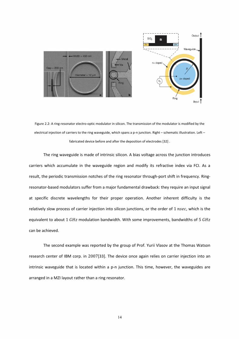
Figure 2.2: A ring-resonator electro-optic modulator in silicon. The transmission of the modulator is modified by the
electrical injection of carriers to the ring waveguide, which spans a p-n junction. Right – schematic illustration. Left –
fabricated device before and after the deposition of electrodes [32] .
The ring waveguide is made of intrinsic silicon. A bias voltage across the junction introduces
carriers which accumulate in the waveguide region and modify its refractive index via FCI. As a
result, the periodic transmission notches of the ring resonator through-port shift in frequency. Ring-
resonator-based modulators suffer from a major fundamental drawback: they require an input signal
at specific discrete wavelengths for their proper operation. Another inherent difficulty is the
relatively slow process of carrier injection into silicon junctions, or the order of , which is the
equivalent to about modulation bandwidth. With some improvements, bandwidths of
can be achieved.
The second example was reported by the group of Prof. Yurii Vlasov at the Thomas Watson
research center of IBM corp. in [33]. The device once again relies on carrier injection into an
intrinsic waveguide that is located within a p-n junction. This time, however, the waveguides are
arranged in a MZI layout rather than a ring resonator.
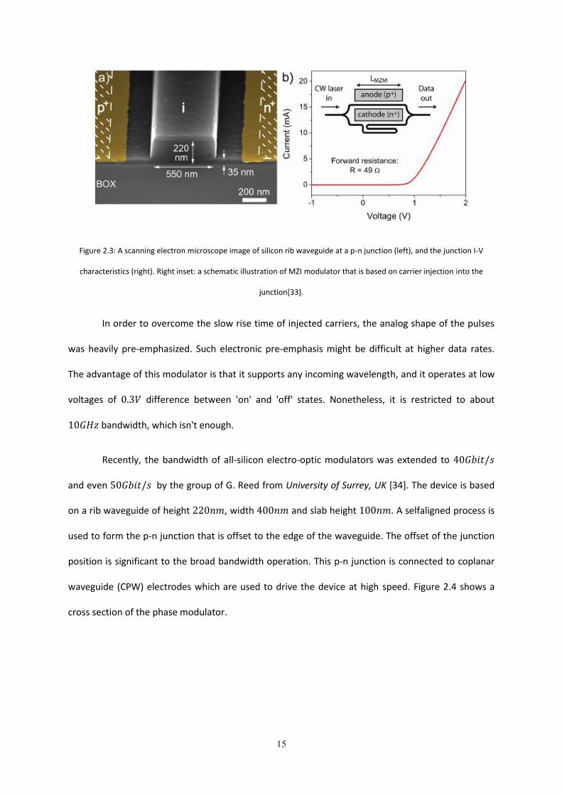
15
Figure 2.3: A scanning electron microscope image of silicon rib waveguide at a p-n junction (left), and the junction I-V
characteristics (right). Right inset: a schematic illustration of MZI modulator that is based on carrier injection into the
junction[33].
In order to overcome the slow rise time of injected carriers, the analog shape of the pulses
was heavily pre-emphasized. Such electronic pre-emphasis might be difficult at higher data rates.
The advantage of this modulator is that it supports any incoming wavelength, and it operates at low
voltages of difference between 'on' and 'off' states. Nonetheless, it is restricted to about
bandwidth, which isn't enough.
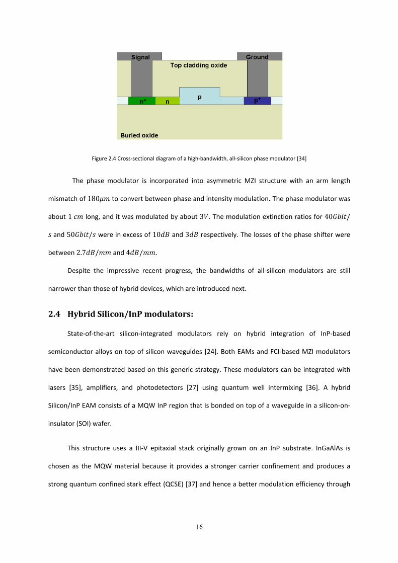
Recently, the bandwidth of all-silicon electro-optic modulators was extended to
and even by the group of G. Reed from University of Surrey, UK [34]. The device is based
on a rib waveguide of height , width and slab height . A selfaligned process is
used to form the p-n junction that is offset to the edge of the waveguide. The offset of the junction
position is significant to the broad bandwidth operation. This p-n junction is connected to coplanar
waveguide (CPW) electrodes which are used to drive the device at high speed. Figure 2.4 shows a
cross section of the phase modulator.
16
Figure 2.4 Cross-sectional diagram of a high-bandwidth, all-silicon phase modulator [34]
The phase modulator is incorporated into asymmetric MZI structure with an arm length
mismatch of to convert between phase and intensity modulation. The phase modulator was
about long, and it was modulated by about . The modulation extinction ratios for
and were in excess of and respectively. The losses of the phase shifter were
between and .
Despite the impressive recent progress, the bandwidths of all-silicon modulators are still
narrower than those of hybrid devices, which are introduced next.
2.4 Hybrid Silicon/InP modulators:
State-of-the-art silicon-integrated modulators rely on hybrid integration of InP-based
semiconductor alloys on top of silicon waveguides [24]. Both EAMs and FCI-based MZI modulators
have been demonstrated based on this generic strategy. These modulators can be integrated with
lasers [35], amplifiers, and photodetectors [27] using quantum well intermixing [36]. A hybrid
Silicon/InP EAM consists of a MQW InP region that is bonded on top of a waveguide in a silicon-on-
insulator (SOI) wafer.
This structure uses a III-V epitaxial stack originally grown on an InP substrate. InGaAlAs is
chosen as the MQW material because it provides a stronger carrier confinement and produces a
strong quantum confined stark effect (QCSE) [37] and hence a better modulation efficiency through
17
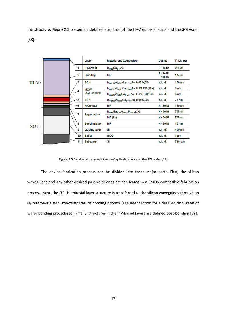
the structure. Figure 2.5 presents a detailed structure of the III–V epitaxial stack and the SOI wafer
[38].
Figure 2.5 Detailed structure of the III–V epitaxial stack and the SOI wafer [38]
The device fabrication process can be divided into three major parts. First, the silicon
waveguides and any other desired passive devices are fabricated in a CMOS-compatible fabrication
process. Next, the – epitaxial layer structure is transferred to the silicon waveguides through an
O2 plasma-assisted, low-temperature bonding process (see later section for a detailed discussion of
wafer bonding procedures). Finally, structures in the InP-based layers are defined post-bonding [39].
18
Figure 2.6 (a) Schematic diagram of device cross section (b) Schematic of the transition taper of a passive silicon waveguide
to an active hybrid section and vice versa. (c) SEM picture of a taper [39].
A hybrid silicon/InP modulator was first demonstrated by the group of J. Bowers at the
University of California at Santa Barbara (UCSB). Their devices required only over a relatively
short length of , along with a bandwidth of and could handle of optical power
[40]. The same group recently extended the modulation bandwidth of their hybrid silicon/InP
devices to beyond ! [38].
2.5 Hybrid Silicon/LiNbO3 modulators:
As stated earlier, the long-term objective of the research program is to try and carry over the
hybrid integration principle described above to the fabrication of silicon/LiNbO3 modulators. In this
section I introduce the general architecture of such devices.
Waveguides made of dielectric materials consist of a high-index core, which is surrounded by
regions of lower index referred to as cladding. The guiding of light is based on its tendency to "be
drawn into" the regions of high refractive index. The optical field propagates in waveguides in the
forms of modes, which are solutions to Maxwell's equations that satisfy the appropriate geometric
boundary conditions. When the contrast in refractive index between core and cladding is large, the
spatial distribution of the guided mode intensity tends to confine itself to the core region .
(a) (b) (c)
19
We use silicon-on-insulator (SOI) wafers as a material platform for the design of a planar
waveguide circuit. An SOI wafer consists of a silicon substrate whose thickness is hundreds of , a
layer of SiO2 (silica), also referred to as buried oxide or BOX, and an upper layer of silicon known as
the device layer. The thickness of the silica layer is typically in the range of , and the device
layer thickness varies between and . SOI wafers offer a particularly large contrast index,
between that of silicon ( ) and that of SiO2 ( ). This index contrast leads to
particularly tight confinement of the modal intensity, which scales down the cross-section of
photonic devices to hundreds of nanometers level. The silica layer has a critical role in preventing
the leaking of the modal energy into the underlying bulk silicon substrate.
On top of the SOI, we intend to bond a bulk of LiNbO3 ( ), in which electro-optic
modulation takes place. The integrated device should be designed to support a single hybrid mode,
and to maximize the overlap of the transverse profile of this mode with the LiNbO3 layer. Electrodes
are deposited for the application of modulation voltage across the device. The voltage would modify
the refractive index of the upper LiNbO3 cladding layer, and hence the effective index of the hybrid
mode as a whole and the accumulated phase in propagation along the device. Figure 2.7 shows a
schematic illustration of the cross-section of the proposed hybrid device.
Figure 2.7 A schematic drawing of the cross section of the hybrid modulator
21
As mentioned above, the combination of mature and well established manufacturing
industry and passive waveguides properties of silicon and the electro-optic properties of Lithium
Niobate appears an appealing approach towards hybrid electro optic modulators. On the other
hand, LiNbO3 and silicon have very different thermal expansion coefficients, which prevent the
evaporation of LiNbO3 on silicon [14]. Therefore careful bonding techniques are necessary for such
integration.
2.5.1 Bonding techniques for use in silicon photonics
The two main methods for bonding dissimilar electro-optic materials are direct bonding and
adhesive bonding using polymers. Direct bonding is carried out without any additional intermediate
layers. When clean and activated, mirror polished, flat surfaces are put one on top of the other
under pressure and heat, hydrogen bonds can initially form across the two surfaces. Following
annealing at high temperatures between , the hydrogen may be released and covalent
bonds may form instead [41]. Adhesive-based bonding employs an intermediate thermosetting
polymer layer such as benzocyclobutene (BCB) based polymers. In BCB-mediated bonding, a diluted
oligomer solution is first spin-coated on the surface of one sample. The solvent is then evaporated,
the two samples are attached and the adhesive is cured [42].
Although both methods are successfully employed, for example, in the fabrication of hybrid
silicon-InP electro-optic devices, they are not without drawbacks. Direct bonding suffers from out-
gassing of by-products such as hydrogen or water which can lead to local de-bonding. It also does
not tolerate even modest levels of contamination and surface roughness. In the case of direct
bonding of silicon and LiNbO3, the thermal expansion coefficients mismatch between the two
materials would induce excessive thermal stresses. BCB-based bonding results is a relatively thick
interface which can hinder the coupling of light and the thermal conductivity across the interface.
Therefore, new methods should be explored for the bonding of silicon and LiNbO3.
21
2.5.2 Reported attempts for bonding silicon and LiNbO3
There are several reports of bonding these two materials together in the literature [8–13].
The first two use thin layers of LiNbO3 that are transferred onto silicon substrates using ion
implantation and subsequent silver diffusion or laser irradiation [8,9]. In one method layer transfer
was induced by laser irradiation in conjunction with ion implantation. The technique was developed
by the group of Harry A. Atwater from California Institute of Technology [8]. High-dose and high-
energy H+ and He+ co-implantation is used to synthesize a buried damage layer in the LiNbO3 bulk
crystal, which is bonded to the Si substrate. After bonding, high power CW-CO2 laser-irradiation
leads to formation and lateral propagation of gas microcavities at the buried damage layer through
the rapid absorption of radiation and heat, eventually leading to localized layer exfoliation from the
LiNbO3 donor substrate. Large-area single-crystal LiNbO3 thin films ( , thick)
have been transferred to silicon substrates. However, this method creates cracks along particular
orientations of the LiNbO3 thin film. In addition, ion implantation is complex and not always
accessible outside specialty foundries.
A second method by the same group was based on silver diffusion bonding and layer
transfer of Lithium-Niobate to silicon [9]. A Lithium-Niobate crystal was co-implanted with hydrogen
and helium ions. Silver was evaporated on both the implanted Lithium Niobate and silicon substrates
and the silvered surfaces were then bonded together at . The high temperature anneal caused
the silver layers to bond together. Simultaneously, the annealing induced crack formation within the
Lithium Niobate at the peak implantation depth. As a result, a layer of Lithium Niobate, whose
thickness corresponds to the peak depth of ion implantation, was transferred to the silicon handle
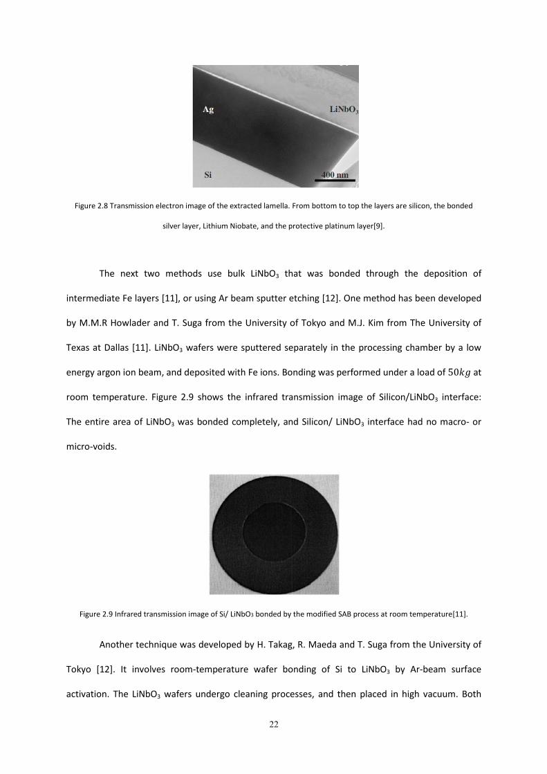
substrate. A transmission electron microscopy image of the bonding interface is shown in Figure 2.8.
The presence of a metallic silver layer at the interface between silicon and LiNbO3 would disrupt the
coupling of light between waveguides each material.
22
Figure 2.8 Transmission electron image of the extracted lamella. From bottom to top the layers are silicon, the bonded
silver layer, Lithium Niobate, and the protective platinum layer[9].
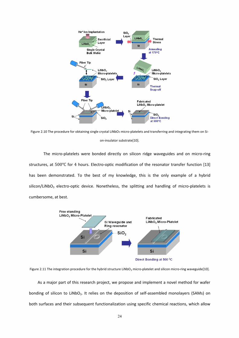
The next two methods use bulk LiNbO3 that was bonded through the deposition of
intermediate Fe layers [11], or using Ar beam sputter etching [12]. One method has been developed
by M.M.R Howlader and T. Suga from the University of Tokyo and M.J. Kim from The University of
Texas at Dallas [11]. LiNbO3 wafers were sputtered separately in the processing chamber by a low
energy argon ion beam, and deposited with Fe ions. Bonding was performed under a load of at
room temperature. Figure 2.9 shows the infrared transmission image of Silicon/LiNbO3 interface:
The entire area of LiNbO3 was bonded completely, and Silicon/ LiNbO3 interface had no macro- or
micro-voids.
Figure 2.9 Infrared transmission image of Si/ LiNbO3 bonded by the modified SAB process at room temperature[11].
Another technique was developed by H. Takag, R. Maeda and T. Suga from the University of
Tokyo [12]. It involves room-temperature wafer bonding of Si to LiNbO3 by Ar-beam surface
activation. The LiNbO3 wafers undergo cleaning processes, and then placed in high vacuum. Both

23
silicon and LiNbO3 specimens were sputter etched simultaneously by Ar beam. After sputter etching,
the specimens were mated in the vacuum chamber, under applied pressure of , however,
fracture from the LiNbO3 bulk was observed after preforming tensile tests.
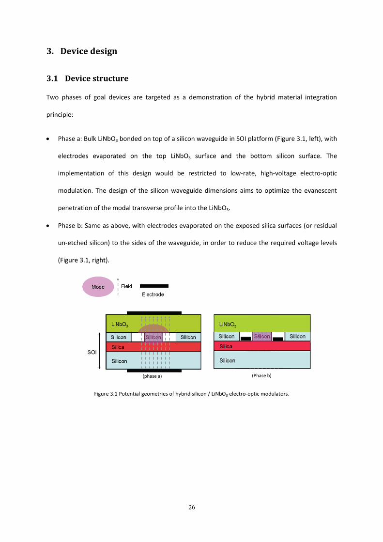
In the next notable example, micron-thick platelets of LiNbO3 were cleaved off a bulk crystal
and directly bonded onto SOI waveguides and resonators [10,13]. It has been developed by the
group of William H. Steier at the University of Southern California (USC) [10]. The process flow is as
follows: He+ ions were implanted into a bulk single crystal LiNbO3 wafer. The implantation energy of
was selected in order to obtain implantation depth of , where a structural defect
layer was formed. The implanted sample was pressed onto a SiO2 coated Si wafer and heated to
in air. Due to the difference in thermal expansion, and because the bonding strength of direct
bonding is very weak at , single crystal LiNbO3 films are separated from bulk LiNbO3 wafer and
are not bonded to the substrate. The free standing single crystal platelets are ~ thick and they
have various widths ( ) and lengths ( ). Many of them are curved at radii
between and , due to stress caused by the crystal damage in the implanted layer. The
platelets can be 'straightened' by high-temperature annealing ( for hours). Individual
micro-platelets can be picked up from the surface by the electro-static attraction between an optical
fiber tip and the platelet, moved to another substrate, positioned, and subsequently bonded to the
new substrate.
24
Figure 2.10 The procedure for obtaining single crystal LiNbO3 micro-platelets and transferring and integrating them on Si-
on-insulator substrate[10].
The micro-platelets were bonded directly on silicon ridge waveguides and on micro-ring
structures, at for hours. Electro-optic modification of the resonator transfer function [13]
has been demonstrated. To the best of my knowledge, this is the only example of a hybrid
silicon/LiNbO3 electro-optic device. Nonetheless, the splitting and handling of micro-platelets is
cumbersome, at best.
Figure 2.11 The integration procedure for the hybrid structure LiNbO3 micro-platelet and silicon micro-ring waveguide[10].
As a major part of this research project, we propose and implement a novel method for wafer
bonding of silicon to LiNbO3. It relies on the deposition of self-assembled monolayers (SAMs) on
both surfaces and their subsequent functionalization using specific chemical reactions, which allow

25
for the bonding of the two surfaces at low temperatures. The bonding is formed through covalent
bonds across the surfaces, via the monolayers. The bonding interface is only a few nm thick, and
does not disrupt optical coupling. Moreover, the relative hydrophobicity of the monolayer coatings
is likely to reduce problems associated with the contamination of surfaces with dust particles.
26
3. Device design
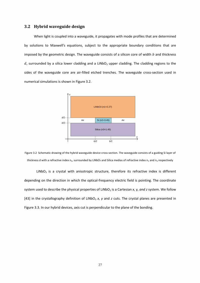
3.1 Device structure
Two phases of goal devices are targeted as a demonstration of the hybrid material integration
principle:
Phase a: Bulk LiNbO3 bonded on top of a silicon waveguide in SOI platform (Figure 3.1, left), with
electrodes evaporated on the top LiNbO3 surface and the bottom silicon surface. The
implementation of this design would be restricted to low-rate, high-voltage electro-optic
modulation. The design of the silicon waveguide dimensions aims to optimize the evanescent
penetration of the modal transverse profile into the LiNbO3.
Phase b: Same as above, with electrodes evaporated on the exposed silica surfaces (or residual
un-etched silicon) to the sides of the waveguide, in order to reduce the required voltage levels
(Figure 3.1, right).
Figure 3.1 Potential geometries of hybrid silicon / LiNbO3 electro-optic modulators.
(phase a) (Phase b)
27
3.2 Hybrid waveguide design
When light is coupled into a waveguide, it propagates with mode profiles that are determined
by solutions to Maxwell's equations, subject to the appropriate boundary conditions that are
imposed by the geometric design. The waveguide consists of a silicon core of width and thickness
, surrounded by a silica lower cladding and a LiNbO3 upper cladding. The cladding regions to the
sides of the waveguide core are air-filled etched trenches. The waveguide cross-section used in
numerical simulations is shown in Figure 3.2.
Silica (n3=1.45)
Si (n2=3.45)
-d/2
d/2
LiNbO3 (n1=2.27)
Air Air
x
y
-b/2 b/2
Figure 3.2 Schematic drawing of the hybrid waveguide device cross-section. The waveguide consists of a guiding Si layer of
thickness d with a refractive index n2, surrounded by LiNbO3 and Silica medias of refractive index n1 and n3 respectively
LiNbO3 is a crystal with anisotropic structure, therefore its refractive index is different
depending on the direction in which the optical-frequency electric field is pointing. The coordinate
system used to describe the physical properties of LiNbO3 is a Cartesian x, y, and z system. We follow
[43] in the crystallography definition of LiNbO3 x, y and z cuts. The crystal planes are presented in
Figure 3.3. In our hybrid devices, axis cut is perpendicular to the plane of the bonding.
28
Figure 3.3 Real-space representation of the x axis, y axis, z axis and of the X cut and Y cut and Z cut LiNbO3 [44].
The and axes, for which the refractive index is the same, are referred to as the ordinary
axes with an ordinary refractive index , whereas the axis is known as the extra-ordinary axis,
with an extra-ordinary refractive index . The values of the two indices are
[45]. For example, let us assume for the moment that the optical-
frequency electric field is in the direction of the x axis of the crystal, and that the mode is
propagating along the z axis. The transverse profile of the refractive index within the device would
be of the form:
2.212
,3.452 2 2 2
,1 , ,
2 2 2 2
1.452
dx
d d b bx yn x y
d d b bx y y
dx
(2)
The exact solution of Maxwell's equations for these boundary conditions cannot be provided
analytically. Numeric simulations are used for calculating profiles and effective indices of the
propagating modes in the hybrid structure, and their overlap with the various structural layers. The
29
parameters that control the mode profile are the operating wavelength, the polarization of the
incoming beam, the thickness and width of the layers, and the crystalline alignment of the LiNbO3
with respect to incoming state of polarization.
Propagating modes may be classified according to the directions of their electric and
magnetic field components:
TE modes (Transverse Electric), which have no electric field in the direction of propagation.
TM modes (Transverse Magnetic), which have no magnetic field in the direction of
propagation.
Hybrid modes, which have both electric and magnetic field components in the direction of
propagation.
Due to the difference in boundary conditions, the propagation constant of a TM mode of a
given order is somewhat different from that of the corresponding TE mode. This phenomenon is
called birefringence, meaning that electric fields aligned at different directions experience a
different effective index inside the waveguide, and hence propagate at different velocities. When
the light at the waveguide input consists of a combination of TE and TM components, each
component would excite the corresponding mode and propagate accordingly. When the TE and TM
components are added together at the output of the waveguide the different phases they had
acquired could lead to substantial distortion. In addition, TE and TM modes could experience
unequal losses. In principle, it is preferable to excite just one mode, either TE or TM. The choice
between the two will take into consideration the strength of the corresponding electro-optic tensor
coefficient, as addressed later.
Another design consideration is the modal confinement , which quantifies the fraction of
optical power that is confined to a specific area in the waveguide. The silicon confinement factor
refers to the fraction of optical power that is confined to the core, and the LiNbO3 confinement
31
factor relates to the optical power that is confined to the upper LiNbO3 Cladding. In general, the
silicon confinement factor increases as the height or width of the silicon waveguide increases, while
the LiNbO3 confinement factor decreases. We are interested in maximizing LiNbO3 confinement
factor, to achieve a stronger modulation effect. At the same time, confinement in silicon cannot
become too small, or else the guided mode would easily diffract into the upper LiNbO3 cladding.
Single mode propagation in the device is also important, since it prevents modal dispersion. Modal
dispersion occurs when the incoming light source excites a multiple propagating modes, with each
projection propagating at a different group velocity. Differences in accumulated delay lead to
waveform distortion. When only a single propagating mode is supported, there is obviously no
modal dispersion. The single-mode condition is met when the waveguide's core size is reduced. The
above consideration can be illustrated through the analytic solution for a simplified, one-
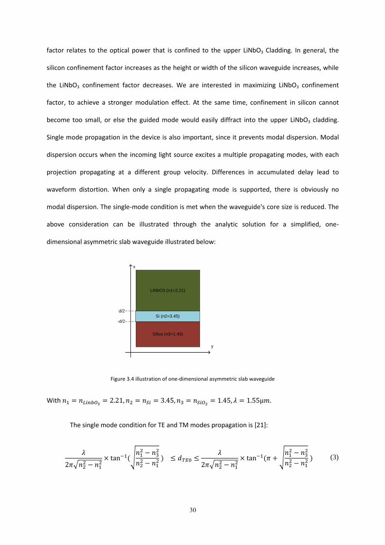
dimensional asymmetric slab waveguide illustrated below:
Silica (n3=1.45)
Si (n2=3.45)
-d/2
d/2
LiNbO3 (n1=2.21)
x
y
Figure 3.4 illustration of one-dimensional asymmetric slab waveguide
With
.
The single mode condition for TE and TM modes propagation is [21]:
√
√
√
√
(3)
31
√
√
√
√
(4)
Where d is the height of the core. Using the above numerical values, we find: 21.76nm
, .
The single-mode condition for the two-dimensional waveguide must be obtained
numerically, and it would depend on both height and width of the silicon core. Nevertheless, the
above values give an order-of-magnitude estimate for the necessary core thickness. Fortunately, the
device layer thickness in most readily-available SOI wafers is , in good agreement with the
above consideration. This is the thickness chosen in my design. The width of the waveguide was
taken initially to be .
Additional key metrics of the devices are mentioned next for completeness, although their
quantitative analysis is beyond the scope of this work. These include the coupling of light into the
hybrid waveguide, propagation losses along the waveguide, and the modulation extinction ratio.
Coupling losses are governed by the flatness and quality of the waveguide facet, and by the
dimensions of the core. Coupling losses between standard fibers and SOI waveguides were reduced
to 1 dB using annular gratings. Propagation losses depend primarily on the nano-scale roughness of
the waveguide sidewalls. Values below 1 dB/cm were obtained. The extinction ratio of the
modulator, signifying the ratio between the output power for '1' and '0' states, is primarily
determined by the driving electronics.
3.2.1 Modulator operation voltage and length calculation
Due to the Pockels effect in LiNbO3, the application of an electric field changes the refractive
index of the material. In the following a quantitative description of the index modification is
provided. The effect can be analyzed within the framework of the index ellipsoid formalism. The
index ellipsoid is a useful geometric interpretation of the refractive index for the propagation of light
in a given medium, as a function of the direction of propagation, state of polarization and crystalline
32
orientation in the medium. In the most general case, the ellipsoid is a surface in a three-dimensional
Cartesian space that is defined by the following equation:
(5)
The index ellipsoid serves to describe the optical propagation properties within an
anisotropic material as follows: For a given propagation vector ⃗⃗ , a plane perpendicular to ⃗⃗ is
drawn through the center of the ellipsoid. The plane intersects the surface of the ellipsoid, forming
an ellipse. The lengths of the long and short axes of this ellipse provide the two possible values for
the material refractive index for the given propagation direction. The orientation of these axes
represents the states of polarization of the two associated vectors.
In the specific case of the LiNbO3 crystal, and in the absence of an external field, the index
ellipsoid of the is of the simpler form [19]:
2 2 2
2 2 2
0 0
1e
x y z
n n n , (6)
where the coefficients of the ellipsoid equations are readily identified in relation to the refractive
indices for light polarized along each of the axes: 2
1 2 01 n and 2
3 1 en . The ordinary index
corresponds to light that is polarized along the x or y axes whereas the extra-ordinary index
relates to a z-polarized field.
Subject to an external electric field vector , the lowest-order modifications to the
index ellipsoid coefficients are governed by the coefficients of the electro-optic tensor :
i ij j
j
r E (7)
The tensor of LiNbO3 is of the form:

33
22 13
22 13
33
42
42
22
0
0
0 0
0 0
0 0
0 0
ij
r r
r r
rr
r
r
r
(8)
For example, the index ellipsoid index subject to the application of an external field along
the z-axis becomes:
2 2 2
13 13 332 2 2
0 0
1 1 11z z z
e
x r E y r E z r En n n
(9)
We can recognize in the modified equation new equivalent values for the refractive indices for the
three directions of propagating optical fields in the crystal:
13 13 332 2 2 2 2 2
0 0
1 1 1 1 1 1, ,z z z
x y z e
r E r E r En n n n n n
(10)
Where 2.21, 2.138@ 1.55o en n m (1)(2), 13 9.6
pmr
V and
33 30.88pm
rV
[45,46].
Since the modifications to the refractive index are generally small, they can be approximated
by:
233
3
3312
33
1
21 e z
ez e e zn r E
e z
nn n n r E
n r E
3
33
1
2z z e e zn n n n r E
(11)
3
, , 13
1
2x y x y o o zn n n n r E (12)
3
, 13
1
2x y o o zn n n r E
(13)
34
We would choose the alignment of the LiNbO3 crystal and the state of polarization of the
incoming optical field so that the electro-optic index modulation is maximized.
Consider a uniform electric field,z
VE
d , where is the voltage that falls across the LiNbO3,
and is the effective thickness of the LiNbO3 that is between the electrodes. The electro-optic phase
modulation following propagation in the waveguide of length is:
2 V
n LV
(14)
Here, is defined as the voltage that is required for a phase shift. For the specific example:
3
33e
dV
n r L
(15)
The primary figure of merit of an electro-optic modulator is the product , which should
be made as small as possible. The device geometry will be designed towards that objective. As
discussed earlier, a phase modulator can be embedded with a MZI to provide intensity modulation.
Figure 3.5 - MZI using the electro optic modulator
Two different designs will be considered. In both, as will be addressed shortly, the properties
of the optical mode are such that the optical-frequency electric field lies in parallel to the bonding
interface. The crystalline alignment, however, would be different between the two designs. In phase
design, where the electrodes are placed on the top and bottom surface of the hybrid device as
35
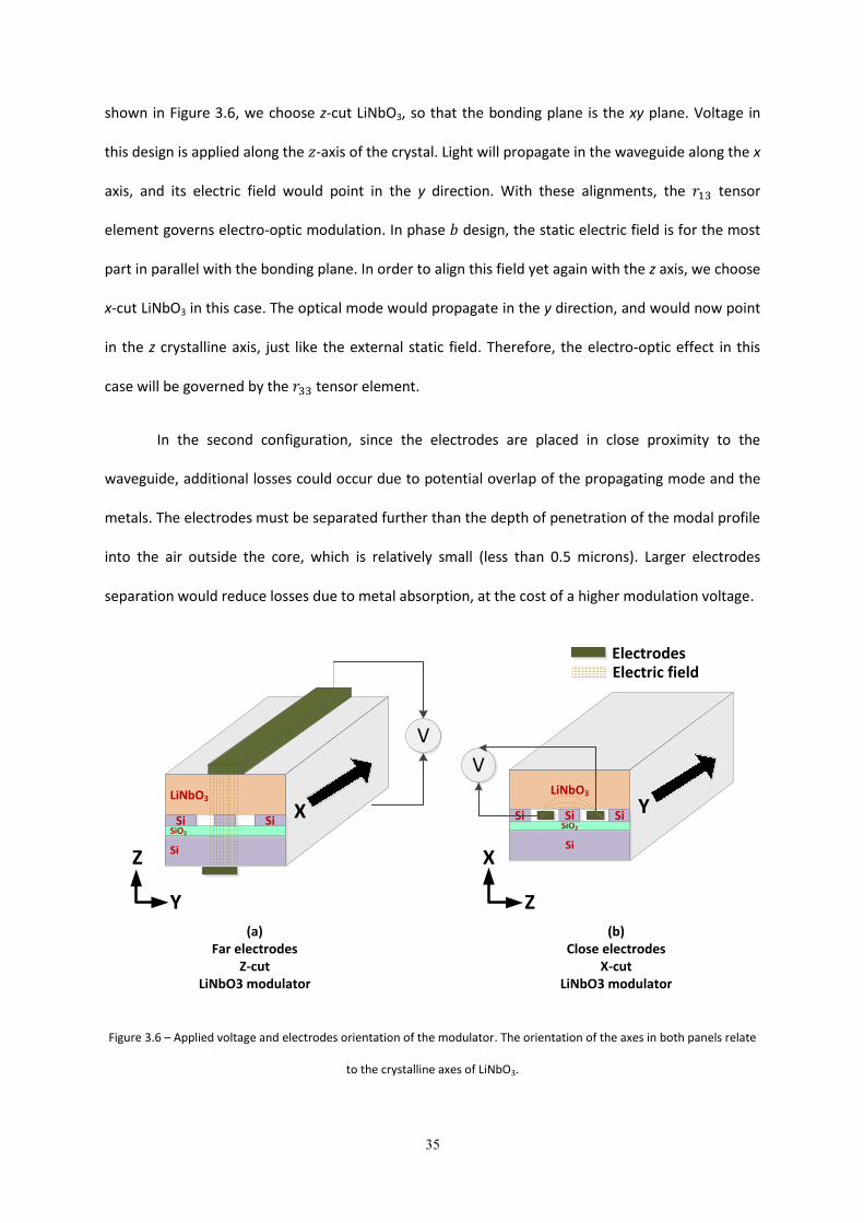
shown in Figure 3.6, we choose z-cut LiNbO3, so that the bonding plane is the xy plane. Voltage in
this design is applied along the -axis of the crystal. Light will propagate in the waveguide along the x
axis, and its electric field would point in the y direction. With these alignments, the tensor
element governs electro-optic modulation. In phase design, the static electric field is for the most
part in parallel with the bonding plane. In order to align this field yet again with the z axis, we choose
x-cut LiNbO3 in this case. The optical mode would propagate in the y direction, and would now point
in the z crystalline axis, just like the external static field. Therefore, the electro-optic effect in this
case will be governed by the tensor element.
In the second configuration, since the electrodes are placed in close proximity to the
waveguide, additional losses could occur due to potential overlap of the propagating mode and the
metals. The electrodes must be separated further than the depth of penetration of the modal profile
into the air outside the core, which is relatively small (less than 0.5 microns). Larger electrodes
separation would reduce losses due to metal absorption, at the cost of a higher modulation voltage.
Figure 3.6 – Applied voltage and electrodes orientation of the modulator. The orientation of the axes in both panels relate
to the crystalline axes of LiNbO3.
V
Z
Y
X
(a)Far electrodes
Z-cutLiNbO3 modulator
V
(b)Close electrodes
X-cutLiNbO3 modulator
X
Z
Y
Electrodes
LiNbO3
Si
SiO2
Si SiSi
LiNbO3
Si
SiSiSiO2
Electric field
36
3.2.2 Waveguide dimensions
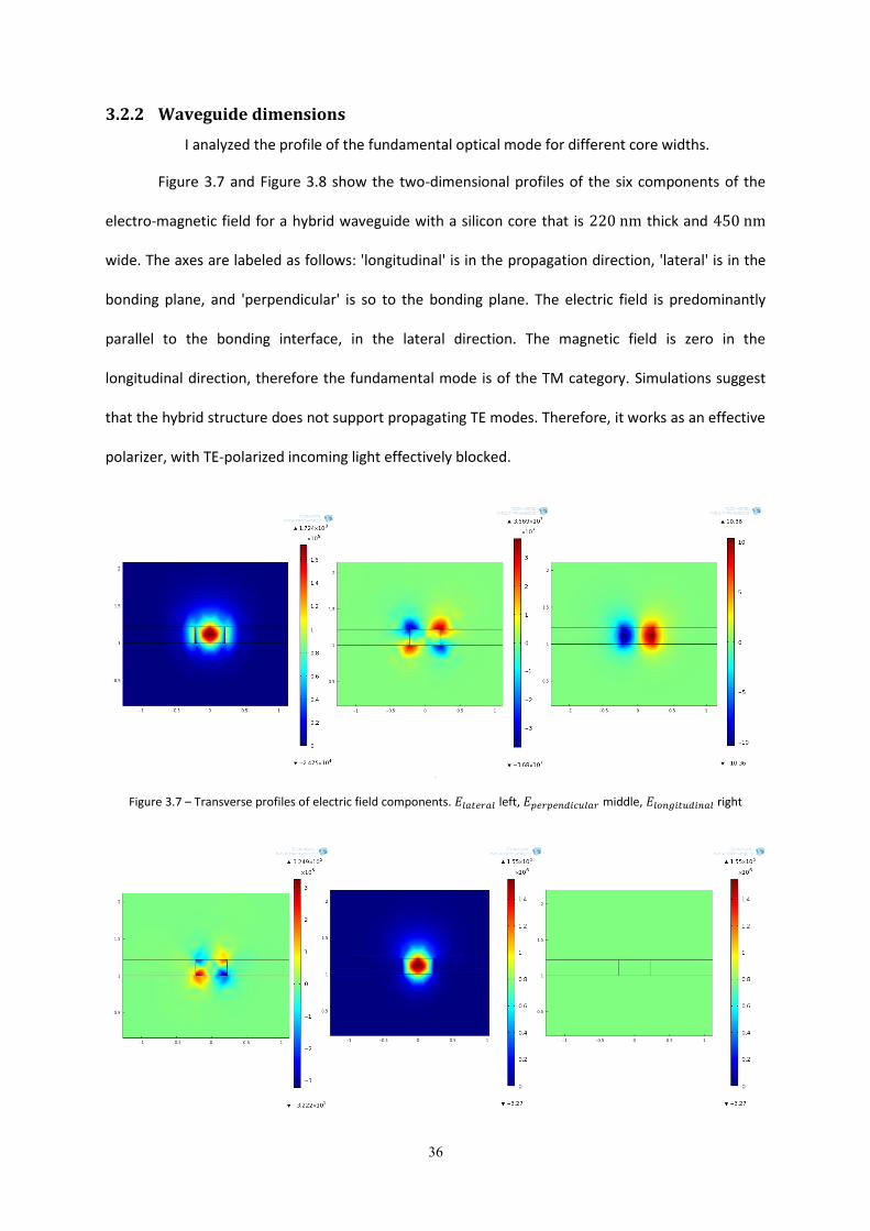
I analyzed the profile of the fundamental optical mode for different core widths.
Figure 3.7 and Figure 3.8 show the two-dimensional profiles of the six components of the
electro-magnetic field for a hybrid waveguide with a silicon core that is thick and
wide. The axes are labeled as follows: 'longitudinal' is in the propagation direction, 'lateral' is in the
bonding plane, and 'perpendicular' is so to the bonding plane. The electric field is predominantly
parallel to the bonding interface, in the lateral direction. The magnetic field is zero in the
longitudinal direction, therefore the fundamental mode is of the TM category. Simulations suggest
that the hybrid structure does not support propagating TE modes. Therefore, it works as an effective
polarizer, with TE-polarized incoming light effectively blocked.
x
Figure 3.7 – Transverse profiles of electric field components. left, middle, right
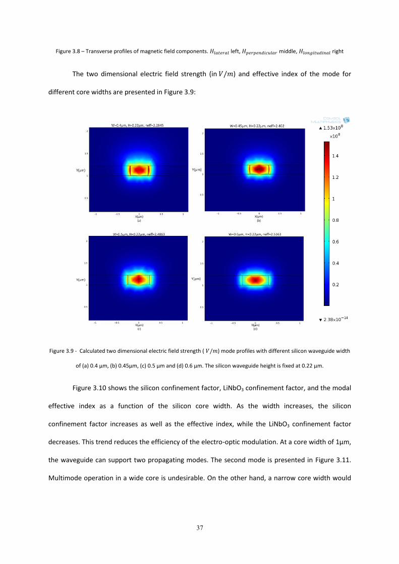
37
Figure 3.8 – Transverse profiles of magnetic field components. left, middle, right
The two dimensional electric field strength (in ) and effective index of the mode for
different core widths are presented in Figure 3.9:
Figure 3.9 - Calculated two dimensional electric field strength ( ) mode profiles with different silicon waveguide width
of (a) 0.4 μm, (b) 0.45μm, (c) 0.5 μm and (d) 0.6 μm. The silicon waveguide height is fixed at 0.22 μm.
Figure 3.10 shows the silicon confinement factor, LiNbO3 confinement factor, and the modal
effective index as a function of the silicon core width. As the width increases, the silicon
confinement factor increases as well as the effective index, while the LiNbO3 confinement factor
decreases. This trend reduces the efficiency of the electro-optic modulation. At a core width of 1µm,
the waveguide can support two propagating modes. The second mode is presented in Figure 3.11.
Multimode operation in a wide core is undesirable. On the other hand, a narrow core width would
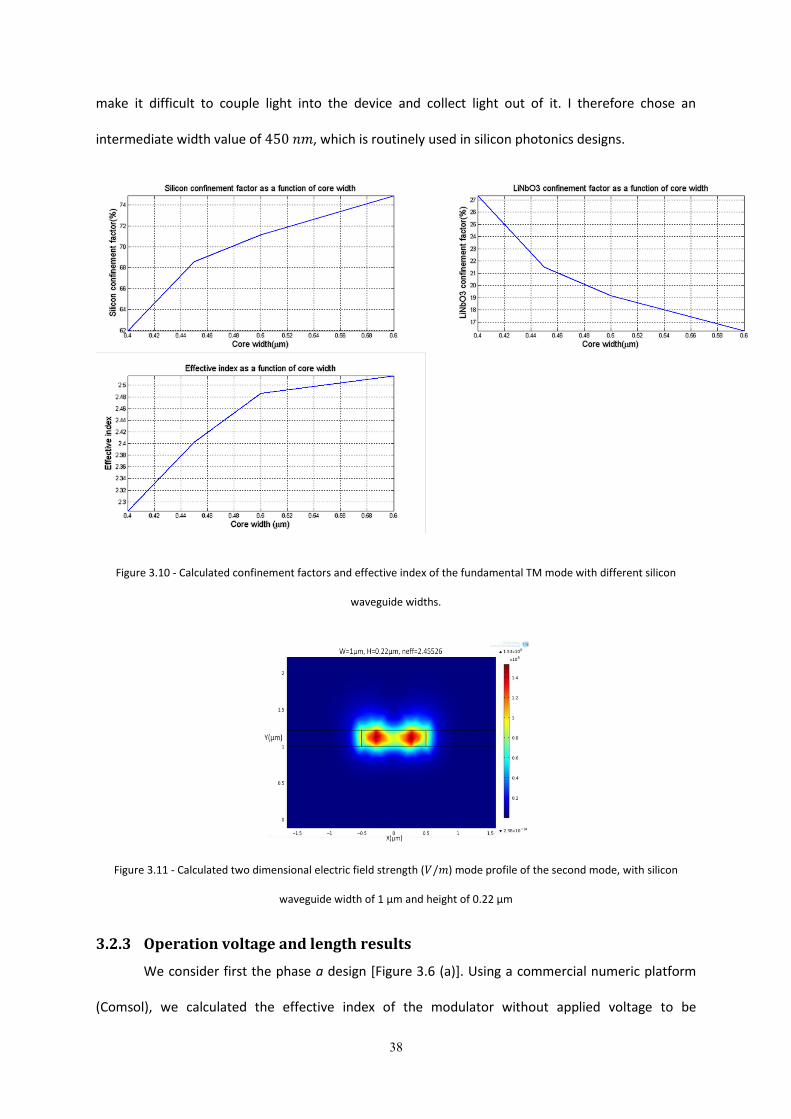
38
make it difficult to couple light into the device and collect light out of it. I therefore chose an
intermediate width value of , which is routinely used in silicon photonics designs.
Figure 3.10 - Calculated confinement factors and effective index of the fundamental TM mode with different silicon
waveguide widths.
Figure 3.11 - Calculated two dimensional electric field strength ( ) mode profile of the second mode, with silicon
waveguide width of 1 μm and height of 0.22 μm
3.2.3 Operation voltage and length results
We consider first the phase a design [Figure 3.6 (a)]. Using a commercial numeric platform
(Comsol), we calculated the effective index of the modulator without applied voltage to be
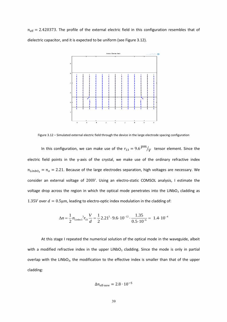
39
. The profile of the external electric field in this configuration resembles that of
dielectric capacitor, and it is expected to be uniform (see Figure 3.12).
Figure 3.12 – Simulated external electric field through the device in the large electrode spacing configuration
In this configuration, we can make use of the
⁄ tensor element. Since the
electric field points in the y-axis of the crystal, we make use of the ordinary refractive index
. Because of the large electrodes separation, high voltages are necessary. We
consider an external voltage of . Using an electro-static COMSOL analysis, I estimate the
voltage drop across the region in which the optical mode penetrates into the LiNbO3 cladding as
over , leading to electro-optic index modulation in the cladding of:
3 3 12 4
3 33 6
1 1 1.352.21 9.6 10 1.4 10
2 2 0.5 10Linbo
Vn n r
d
At this stage I repeated the numerical solution of the optical mode in the waveguide, albeit
with a modified refractive index in the upper LiNbO3 cladding. Since the mode is only in partial
overlap with the LiNbO3, the modification to the effective index is smaller than that of the upper
cladding:
41
The estimated device length that is required for the given voltage is
, or
.
I repeated the electro-static analysis for the phase b design [Figure 3.6 (b)], having close
electrodes spacing. In this configuration, we make use of the tensor element, and since the
electric field points in the z-axis of the crystal the relevant refractive index is now
. Figure 3.13 shows the distribution of an external static electric field, applied across the
electrodes. Within the region that is in overlap with the optical mode, this field is predominantly
aligned in parallel with the bonding interface plane. The external voltage in this configuration is
much smaller due to the close spacing of the electrodes. A value of was chosen. The electro-
static analysis suggests that about drop across the lateral extent of the optical
field. The corresponding device length for -phase modulation is , or . The
close spacing of the electrodes allows for an improvement in the device metrics by over a factor of
. For comparison, the value of in standard LiNbO3 modulators is between ,
depending of the orientation of the crystal [5,47]. The tight modal confinement in a high-index-
contrast SOI waveguide allows, in principle, for a closer electrodes separation than that of standard
devices. That close spacing might be offsetting, to a large extent, the degradation due to the
relatively small penetration of the mode profile into the LiNbO3 cladding.
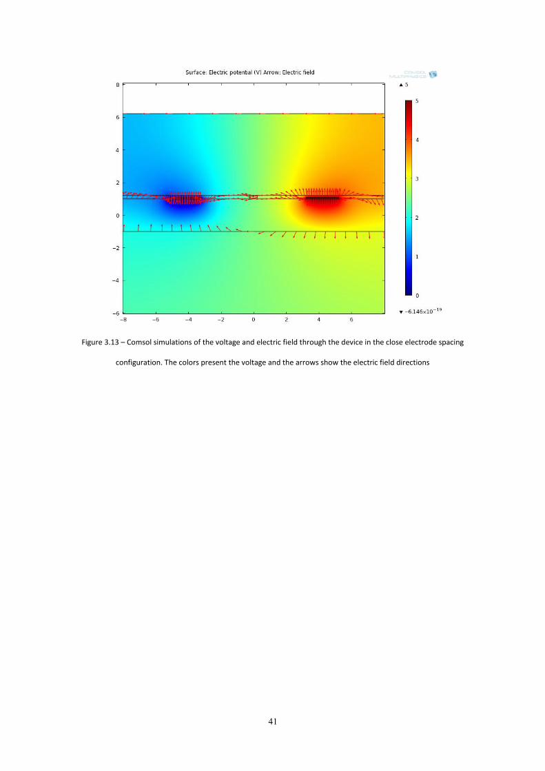
41
Figure 3.13 – Comsol simulations of the voltage and electric field through the device in the close electrode spacing
configuration. The colors present the voltage and the arrows show the electric field directions
42
4. Wafer bonding using self-assembled monolayers
4.1 Bonding between silicon and LiNbO3
In addition to the design and simulation of hybrid modulator performance, the work also
addressed the main fabrication challenge of hybrid devices: the bonding of LiNbO3 to silicon. The
bonding must meet several requirements:
The interface has to be strong and durable for a long time. It must also withstand the post-
bonding processes of waveguide fabrication (evaporation of contacts etc.).
The process should have potential for commercial scaling.
A thin bonding interface is necessary (< ), to allow for effective coupling of light
between structures in both materials.
As discussed at length in the previous section, the bonding between the two materials is
difficult and challenging. Only few reports are provided in the literature, and only a single report
describes the making of a hybrid device. Even that work required the splitting of micro-platelets of
LiNbO3 in a cumbersome procedure that is difficult to scale. In particular, use of direct bonding
procedures with relatively high annealing temperatures is prohibited due to large thermal stresses.
Alternatively, we proposed and attempted a new paradigm for the bonding process, which is
assisted by the deposition of single molecular layers of specially-synthesized organic materials on the
surfaces of both substrates. The deposition occurs spontaneously in a solution which contains the
monolayer-making molecules, in a process that is referred to as self-assembly [48]. Hence the term
self-assembled monolayers (SAMs) is used in the following in relation to the bonding mechanism.
While one terminus of the molecule is designed to attach to the substrate, the functional chemical
group at the opposite terminus remains free-standing and defines the chemistry of a modified
surface. The resulting dense and orderly array of these functional groups can be regarded as a
43
specialized form of surface activation. Following deposition, the functional groups are modified
through chemical reaction, and brought into a form that readily attaches to the opposite modified
substrate.
Before addressing the details of the deposition and activation processes, I will briefly
introduce the field of SAMs, and the specific molecule that is underlying our procedures.
4.2 Self-assembled Monolayer (SAM):
Self-assembly is a process by which an organized structure can spontaneously form from
simple parts on a variety of surfaces [49]. Self-assembled monolayers (SAMs) are highly ordered
two-dimensional structures that are strongly anchored to a surface. Although these films are
extremely thin (typically ), they are able to completely change the surface properties. The most
common adsorbate/substrate combinations are alkylsilanes on oxide surfaces [50], and sulfur-
containing molecules on gold [51].
Since the first report on SAMs in 1983 by Lucy Netzer and Jacob Sagiv [50], the field of SAMs
on Silicon oxide surfaces has grown immensely. Self-assembled monolayers on silicon oxide
constitute ordered molecular platforms which can be employed in surface patterning and
nanofabrication techniques, as well as for bio-chemical sensing [32],[33], lubrication[54],
electrochemistry[55] ,photochemical mechanism[56], and electrical conduction[57] .
The interaction between two monolayers deposited on opposing solid substrates, in order to
form covalent bonds between the two organic monolayers, was studied by the group of Prof. U.
Gosele at Max Plank Institute in Halle, Germany. The group reported the SAM-assisted bonding of
two silicon wafers [58]. We demonstrate herein a modification of this methodology which takes
advantage of controlled surface chemistry on well-defined functionalized monolayers and extends
this bonding paradigm to non-silicon, optically active, materials, such as LiNbO3 [59].
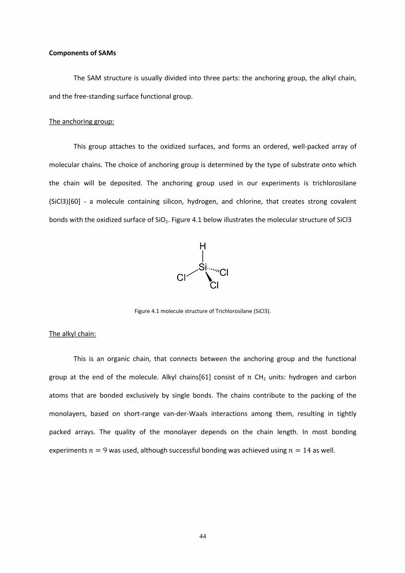
44
Components of SAMs
The SAM structure is usually divided into three parts: the anchoring group, the alkyl chain,
and the free-standing surface functional group.
The anchoring group:
This group attaches to the oxidized surfaces, and forms an ordered, well-packed array of
molecular chains. The choice of anchoring group is determined by the type of substrate onto which
the chain will be deposited. The anchoring group used in our experiments is trichlorosilane
(SiCl3)[60] - a molecule containing silicon, hydrogen, and chlorine, that creates strong covalent
bonds with the oxidized surface of SiO2. Figure 4.1 below illustrates the molecular structure of SiCl3
Figure 4.1 molecule structure of Trichlorosilane (SiCl3).
The alkyl chain:
This is an organic chain, that connects between the anchoring group and the functional
group at the end of the molecule. Alkyl chains[61] consist of CH2 units: hydrogen and carbon
atoms that are bonded exclusively by single bonds. The chains contribute to the packing of the
monolayers, based on short-range van-der-Waals interactions among them, resulting in tightly
packed arrays. The quality of the monolayer depends on the chain length. In most bonding
experiments was used, although successful bonding was achieved using as well.
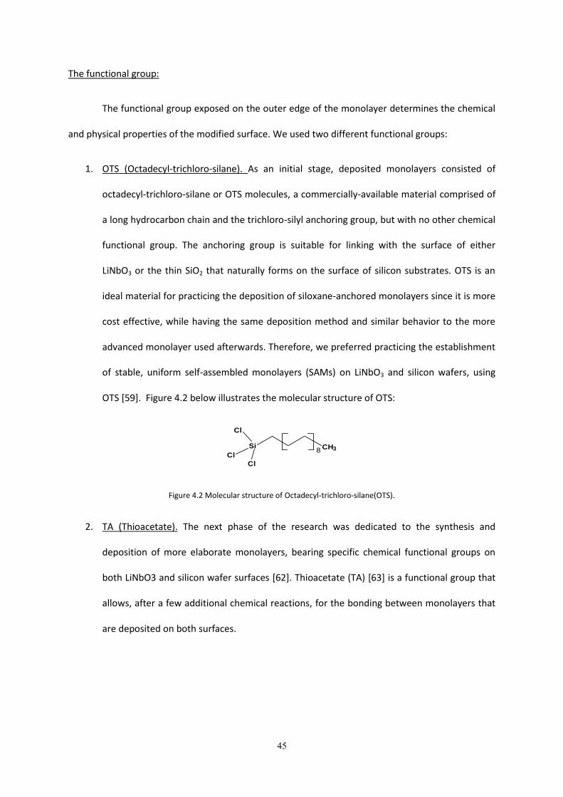
45
The functional group:
The functional group exposed on the outer edge of the monolayer determines the chemical
and physical properties of the modified surface. We used two different functional groups:
1. OTS (Octadecyl-trichloro-silane). As an initial stage, deposited monolayers consisted of
octadecyl-trichloro-silane or OTS molecules, a commercially-available material comprised of
a long hydrocarbon chain and the trichloro-silyl anchoring group, but with no other chemical
functional group. The anchoring group is suitable for linking with the surface of either
LiNbO3 or the thin SiO2 that naturally forms on the surface of silicon substrates. OTS is an
ideal material for practicing the deposition of siloxane-anchored monolayers since it is more
cost effective, while having the same deposition method and similar behavior to the more
advanced monolayer used afterwards. Therefore, we preferred practicing the establishment
of stable, uniform self-assembled monolayers (SAMs) on LiNbO3 and silicon wafers, using
OTS [59]. Figure 4.2 below illustrates the molecular structure of OTS:
Si
Cl
Cl
Cl
CH38
Figure 4.2 Molecular structure of Octadecyl-trichloro-silane(OTS).
2. TA (Thioacetate). The next phase of the research was dedicated to the synthesis and
deposition of more elaborate monolayers, bearing specific chemical functional groups on
both LiNbO3 and silicon wafer surfaces [62]. Thioacetate (TA) [63] is a functional group that
allows, after a few additional chemical reactions, for the bonding between monolayers that
are deposited on both surfaces.
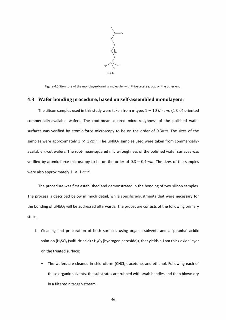
46
Figure 4.3 Structure of the monolayer-forming molecule, with thioacetate group on the other end.
4.3 Wafer bonding procedure, based on self-assembled monolayers:
The silicon samples used in this study were taken from n-type, , oriented
commercially-available wafers. The root-mean-squared micro-roughness of the polished wafer
surfaces was verified by atomic-force microscopy to be on the order of . The sizes of the
samples were approximately . The LiNbO3 samples used were taken from commercially-
available -cut wafers. The root-mean-squared micro-roughness of the polished wafer surfaces was
verified by atomic-force microscopy to be on the order of . The sizes of the samples
were also approximately .
The procedure was first established and demonstrated in the bonding of two silicon samples.
The process is described below in much detail, while specific adjustments that were necessary for
the bonding of LiNbO3 will be addressed afterwards. The procedure consists of the following primary
steps:
1. Cleaning and preparation of both surfaces using organic solvents and a ‘piranha’ acidic
solution (H2SO4 (sulfuric acid) : H2O2 (hydrogen peroxide)), that yields a 1nm thick oxide layer
on the treated surface:
The wafers are cleaned in chloroform (CHCl3), acetone, and ethanol. Following each of
these organic solvents, the substrates are rubbed with swab handles and then blown dry
in a filtered nitrogen stream .

47
A ‘piranha’ solution (H2SO4 (sulfuric acid) : H2O2 (hydrogen peroxide)) at a ratio is
prepared.
The wafers are immersed in the piranha solution test tube for minutes, in a
temperature of . This treatment cleans the surface from organic contaminants.
After the wafers are taken off the piranha solution, they are rinsed three times with
deionized (DI), distilled water.
The wafers are immersed in 4% Hydrofluoric acid (HF) solution for minutes followed by
DI water rinse and blown dry using filtered nitrogen. The HF solution removes native
oxide layer from the Si surface.
The wafers are again immersed in Piranha for additional minutes to regrow an oxide
layer. This treatment guarantees that the oxide layer is of known width and enables
better examination by ellipsometry.
After the wafers are taken off the piranha solution, they are rinsed three times with
deionized, distilled water .
The wafers are blown dry under a filtered nitrogen stream.
2. The deposition of the monolayer on both surfaces. The monolayer-forming molecule was
introduced in detail earlier. The molecule and the assembly are illustrated in Figure 4.4.
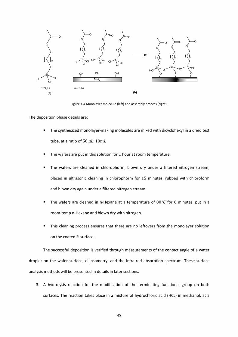
48
Figure 4.4 Monolayer molecule (left) and assembly process (right).
The deposition phase details are:
The synthesized monolayer-making molecules are mixed with dicyclohexyl in a dried test
tube, at a ratio of
The wafers are put in this solution for hour at room temperature.
The wafers are cleaned in chlorophorm, blown dry under a filtered nitrogen stream,
placed in ultrasonic cleaning in chlorophorm for minutes, rubbed with chloroform
and blown dry again under a filtered nitrogen stream.
The wafers are cleaned in n-Hexane at a temperature of for minutes, put in a
room-temp n-Hexane and blown dry with nitrogen.
This cleaning process ensures that there are no leftovers from the monolayer solution
on the coated Si surface.
The successful deposition is verified through measurements of the contact angle of a water
droplet on the wafer surface, ellipsometry, and the infra-red absorption spectrum. These surface
analysis methods will be presented in details in later sections.
3. A hydrolysis reaction for the modification of the terminating functional group on both
surfaces. The reaction takes place in a mixture of hydrochloric acid (HCL) in methanol, at a
(a) (b)
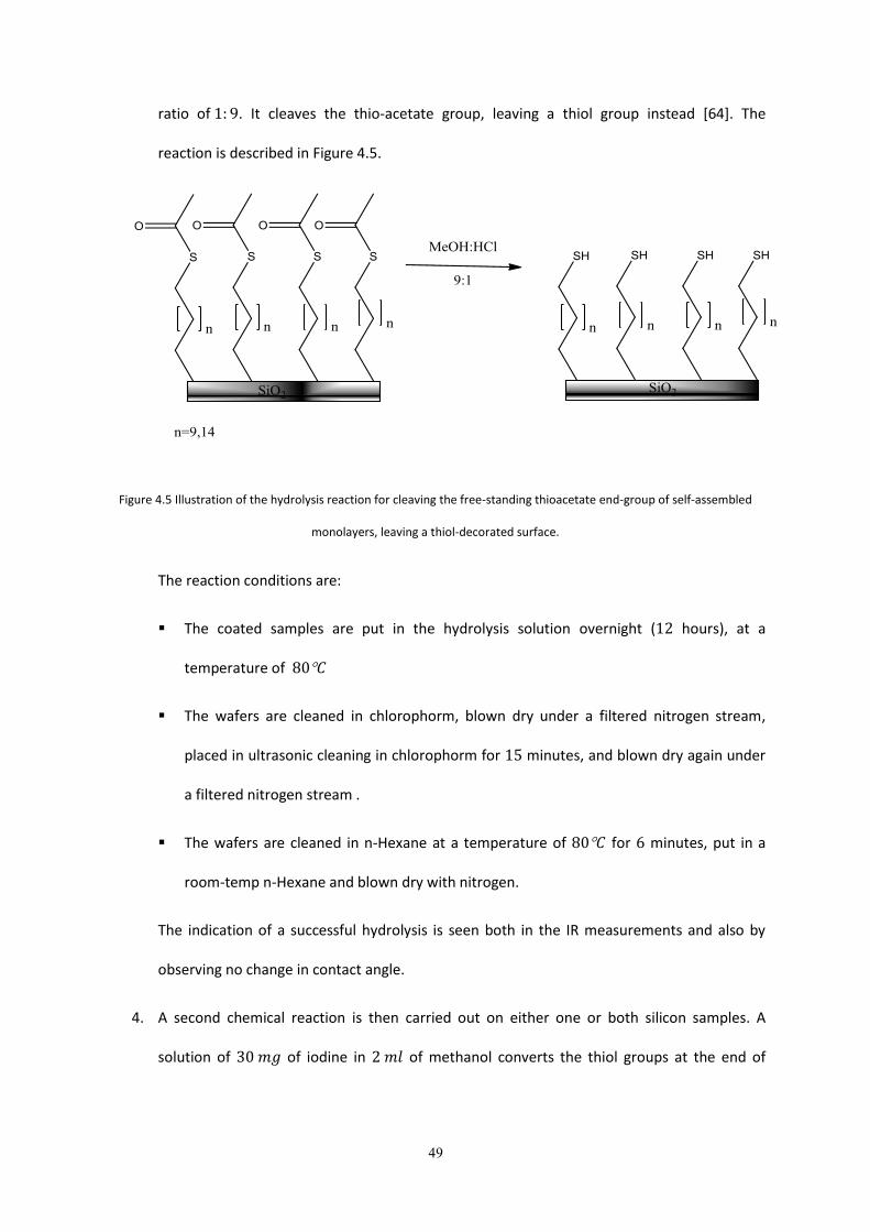
49
ratio of . It cleaves the thio-acetate group, leaving a thiol group instead [64]. The
reaction is described in Figure 4.5.
Figure 4.5 Illustration of the hydrolysis reaction for cleaving the free-standing thioacetate end-group of self-assembled
monolayers, leaving a thiol-decorated surface.
The reaction conditions are:
The coated samples are put in the hydrolysis solution overnight ( hours), at a
temperature of
The wafers are cleaned in chlorophorm, blown dry under a filtered nitrogen stream,
placed in ultrasonic cleaning in chlorophorm for minutes, and blown dry again under
a filtered nitrogen stream .
The wafers are cleaned in n-Hexane at a temperature of for minutes, put in a
room-temp n-Hexane and blown dry with nitrogen.
The indication of a successful hydrolysis is seen both in the IR measurements and also by
observing no change in contact angle.
4. A second chemical reaction is then carried out on either one or both silicon samples. A
solution of of iodine in of methanol converts the thiol groups at the end of

51
some fraction of the molecules to disulphide groups instead [65]. The reaction is illustrated
in Figure 4.6:
Figure 4.6 A reaction for converting Thiol terminating groups to disulphide groups.
The reaction conditions are:
The wafers are put in this solution for 15 minutes at room temperature.
The wafers are rinsed in methanol, inserted to ultrasonic cleaning for 10 minutes in
methanol, and blown dry under a filtered nitrogen stream .
The wafers are cleaned in n-Hexane at a temperature of for 6 minutes, put in a
room-temp n-Hexane and blown dry with nitrogen.
5. Bonding of the two wafers. The bonding takes place within a home-made bonding press,
shown in Figure 4.7.
Figure 4.7 The bonding press closed (left) and the bonding press open (right).
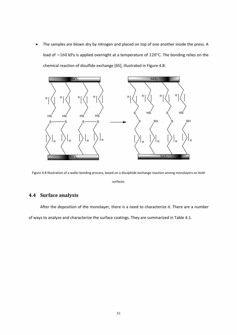
51
The samples are blown dry by nitrogen and placed on top of one another inside the press. A
load of is applied overnight at a temperature of . The bonding relies on the
chemical reaction of disulfide exchange [65], illustrated in Figure 4.8:
Figure 4.8 Illustration of a wafer bonding process, based on a disulphide exchange reaction among monolayers on both
surfaces.
4.4 Surface analysis
After the deposition of the monolayer, there is a need to characterize it. There are a number
of ways to analyze and characterize the surface coatings. They are summarized in Table 4.1.
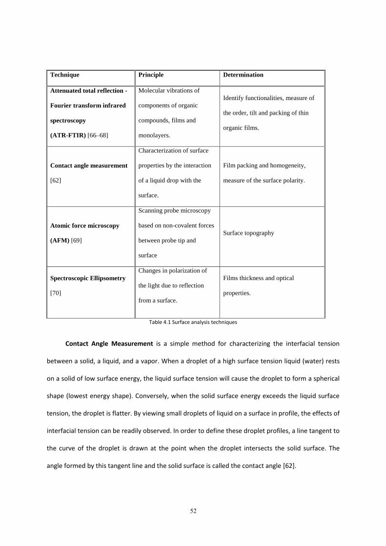
52
Technique Principle Determination
Attenuated total reflection -
Fourier transform infrared
spectroscopy
(ATR-FTIR) [66–68]
Molecular vibrations of
components of organic
compounds, films and
monolayers.
Identify functionalities, measure of
the order, tilt and packing of thin
organic films.
Contact angle measurement
[62]
Characterization of surface
properties by the interaction
of a liquid drop with the
surface.
Film packing and homogeneity,
measure of the surface polarity.
Atomic force microscopy
(AFM) [69]
Scanning probe microscopy
based on non-covalent forces
between probe tip and
surface
Surface topography
Spectroscopic Ellipsometry
[70]
Changes in polarization of
the light due to reflection
from a surface.
Films thickness and optical
properties.
Table 4.1 Surface analysis techniques
Contact Angle Measurement is a simple method for characterizing the interfacial tension
between a solid, a liquid, and a vapor. When a droplet of a high surface tension liquid (water) rests
on a solid of low surface energy, the liquid surface tension will cause the droplet to form a spherical
shape (lowest energy shape). Conversely, when the solid surface energy exceeds the liquid surface
tension, the droplet is flatter. By viewing small droplets of liquid on a surface in profile, the effects of
interfacial tension can be readily observed. In order to define these droplet profiles, a line tangent to
the curve of the droplet is drawn at the point when the droplet intersects the solid surface. The
angle formed by this tangent line and the solid surface is called the contact angle [62].
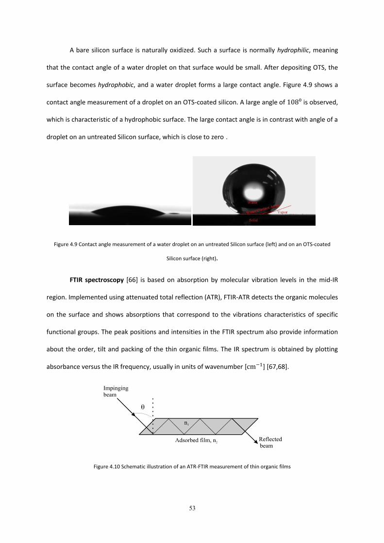
53
A bare silicon surface is naturally oxidized. Such a surface is normally hydrophilic, meaning
that the contact angle of a water droplet on that surface would be small. After depositing OTS, the
surface becomes hydrophobic, and a water droplet forms a large contact angle. Figure 4.9 shows a
contact angle measurement of a droplet on an OTS-coated silicon. A large angle of is observed,
which is characteristic of a hydrophobic surface. The large contact angle is in contrast with angle of a
droplet on an untreated Silicon surface, which is close to zero .
Figure 4.9 Contact angle measurement of a water droplet on an untreated Silicon surface (left) and on an OTS-coated
Silicon surface (right).
FTIR spectroscopy [66] is based on absorption by molecular vibration levels in the mid-IR
region. Implemented using attenuated total reflection (ATR), FTIR-ATR detects the organic molecules
on the surface and shows absorptions that correspond to the vibrations characteristics of specific
functional groups. The peak positions and intensities in the FTIR spectrum also provide information
about the order, tilt and packing of the thin organic films. The IR spectrum is obtained by plotting
absorbance versus the IR frequency, usually in units of wavenumber [ ] [67,68].
Figure 4.10 Schematic illustration of an ATR-FTIR measurement of thin organic films
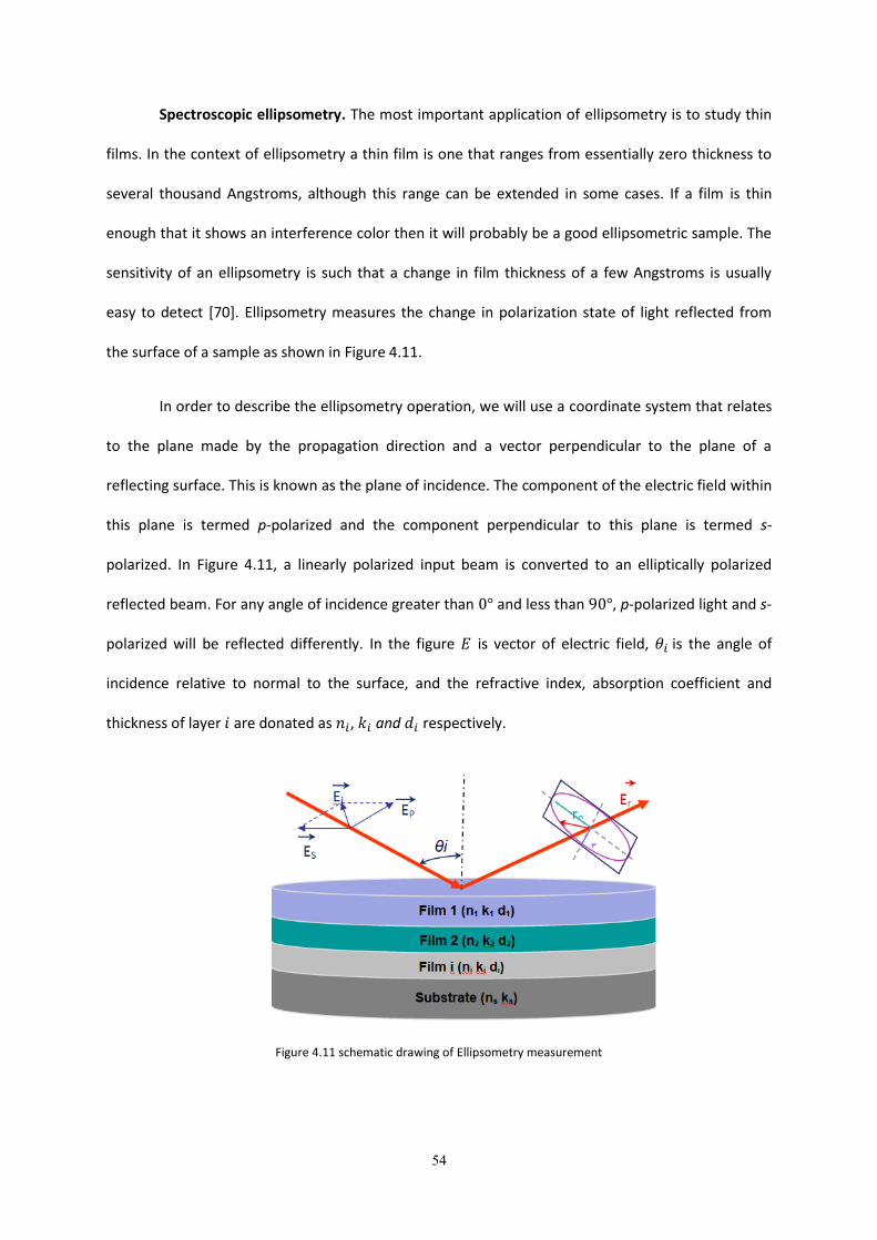
54
Spectroscopic ellipsometry. The most important application of ellipsometry is to study thin
films. In the context of ellipsometry a thin film is one that ranges from essentially zero thickness to
several thousand Angstroms, although this range can be extended in some cases. If a film is thin
enough that it shows an interference color then it will probably be a good ellipsometric sample. The
sensitivity of an ellipsometry is such that a change in film thickness of a few Angstroms is usually
easy to detect [70]. Ellipsometry measures the change in polarization state of light reflected from
the surface of a sample as shown in Figure 4.11.
In order to describe the ellipsometry operation, we will use a coordinate system that relates
to the plane made by the propagation direction and a vector perpendicular to the plane of a
reflecting surface. This is known as the plane of incidence. The component of the electric field within
this plane is termed p-polarized and the component perpendicular to this plane is termed s-
polarized. In Figure 4.11, a linearly polarized input beam is converted to an elliptically polarized
reflected beam. For any angle of incidence greater than and less than , p-polarized light and s-
polarized will be reflected differently. In the figure is vector of electric field, is the angle of
incidence relative to normal to the surface, and the refractive index, absorption coefficient and
thickness of layer are donated as , and respectively.
Figure 4.11 schematic drawing of Ellipsometry measurement
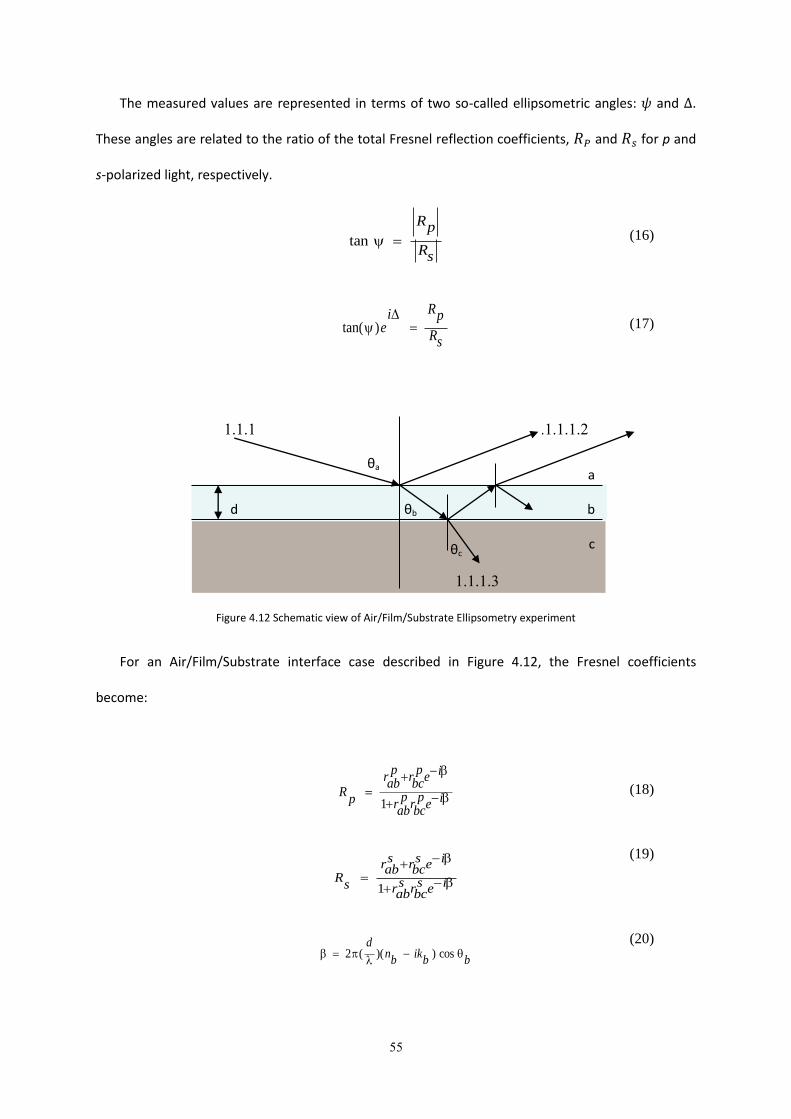
55
The measured values are represented in terms of two so-called ellipsometric angles: and .
These angles are related to the ratio of the total Fresnel reflection coefficients, and for p and
s-polarized light, respectively.
tan
Rp
Rs
(16)
tan( )
Ri pe
Rs
(17)
Figure 4.12 Schematic view of Air/Film/Substrate Ellipsometry experiment
For an Air/Film/Substrate interface case described in Figure 4.12, the Fresnel coefficients
become:
1
p p ir r eab bc
R p p ip r r eab bc
(18)
1
s s ir r eab bcR s s is r r eab bc
(19)
2 ( )( ) cos
dn ik
b b b
(20)
d
1.1.1.1.1.1.1 1.1.1.1.1.1.2
1.1.1.1.1.1.3
θa
θb
θc
a
b
c
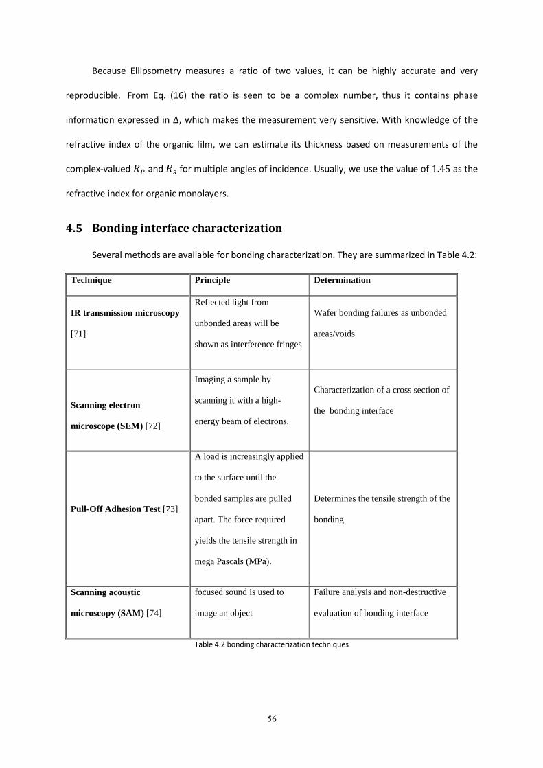
56
Because Ellipsometry measures a ratio of two values, it can be highly accurate and very
reproducible. From Eq. (16) the ratio is seen to be a complex number, thus it contains phase
information expressed in , which makes the measurement very sensitive. With knowledge of the
refractive index of the organic film, we can estimate its thickness based on measurements of the
complex-valued and for multiple angles of incidence. Usually, we use the value of as the
refractive index for organic monolayers.
4.5 Bonding interface characterization
Several methods are available for bonding characterization. They are summarized in Table 4.2:
Technique Principle Determination
IR transmission microscopy
[71]
Reflected light from
unbonded areas will be
shown as interference fringes
Wafer bonding failures as unbonded
areas/voids
Scanning electron
microscope (SEM) [72]
Imaging a sample by
scanning it with a high-
energy beam of electrons.
Characterization of a cross section of
the bonding interface
Pull-Off Adhesion Test [73]
A load is increasingly applied
to the surface until the
bonded samples are pulled
apart. The force required
yields the tensile strength in
mega Pascals (MPa).
Determines the tensile strength of the
bonding.
Scanning acoustic
microscopy (SAM) [74]
focused sound is used to
image an object
Failure analysis and non-destructive
evaluation of bonding interface
Table 4.2 bonding characterization techniques
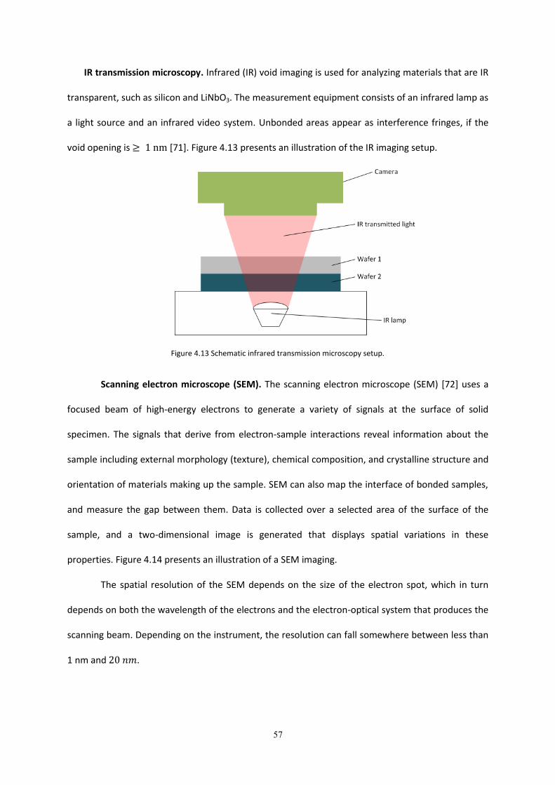
57
IR transmission microscopy. Infrared (IR) void imaging is used for analyzing materials that are IR
transparent, such as silicon and LiNbO3. The measurement equipment consists of an infrared lamp as
a light source and an infrared video system. Unbonded areas appear as interference fringes, if the
void opening is [71]. Figure 4.13 presents an illustration of the IR imaging setup.
Figure 4.13 Schematic infrared transmission microscopy setup.
Scanning electron microscope (SEM). The scanning electron microscope (SEM) [72] uses a
focused beam of high-energy electrons to generate a variety of signals at the surface of solid
specimen. The signals that derive from electron-sample interactions reveal information about the
sample including external morphology (texture), chemical composition, and crystalline structure and
orientation of materials making up the sample. SEM can also map the interface of bonded samples,
and measure the gap between them. Data is collected over a selected area of the surface of the
sample, and a two-dimensional image is generated that displays spatial variations in these
properties. Figure 4.14 presents an illustration of a SEM imaging.
The spatial resolution of the SEM depends on the size of the electron spot, which in turn
depends on both the wavelength of the electrons and the electron-optical system that produces the
scanning beam. Depending on the instrument, the resolution can fall somewhere between less than
1 nm and .
58
Preparation of samples for SEM imaging includes lapping using Struers Labopol-6 standard
lapping machine with low-medium pressure. A SiC paper (grit 500) and ethyl-glycol lapping solution
were used as the abrasive materials for minutes. This aggressive procedure removes more than
from the top wafer. The sample is then cleaved with a diamond pen, and the facet is
cleaned using a focused ion beam.
Figure 4.14 schematic drawing of the electron and x-ray optics of a SEM
Pull-off adhesion test. A commercial adhesion tester, Defelsko Positest AT-A, was used. The
bonded samples were glued to a metal holder on one side and to a transparent window from the
other side, in order to avoid dripping of the slow cure epoxy. The force measurement error
corresponded to an uncertainty of . A tensile force, perpendicular to the bonding
interface, is applied to the metal holder until it is detached. The tensile bond strength (in MPa) is
calculated as the force at failure divided by the bonded area [73]. Figure 4.15 shows the Pull-off
adhesion test equipment

59
Figure 4.15 Pull-off adhesion test equipment
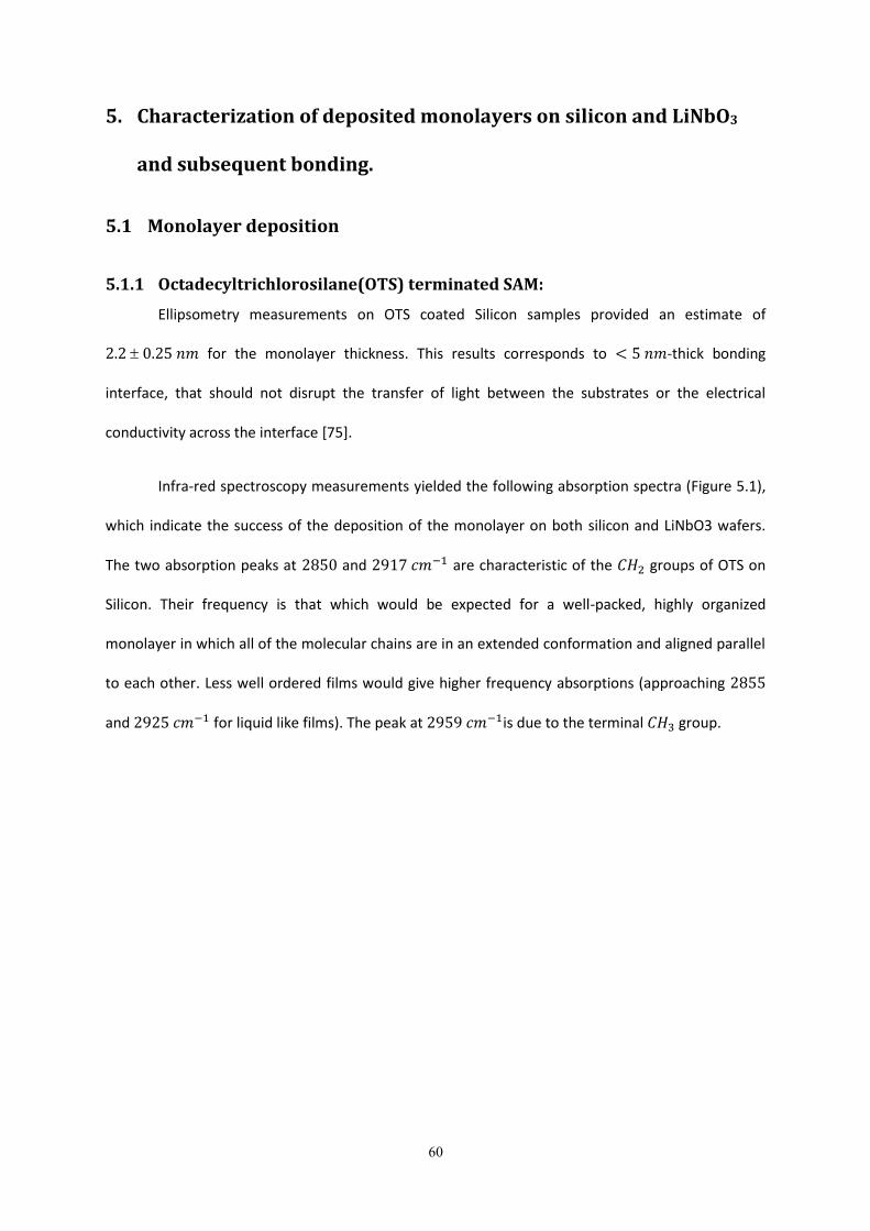
61
5. Characterization of deposited monolayers on silicon and LiNbO3
and subsequent bonding.
5.1 Monolayer deposition
5.1.1 Octadecyltrichlorosilane(OTS) terminated SAM:
Ellipsometry measurements on OTS coated Silicon samples provided an estimate of
for the monolayer thickness. This results corresponds to -thick bonding
interface, that should not disrupt the transfer of light between the substrates or the electrical
conductivity across the interface [75].
Infra-red spectroscopy measurements yielded the following absorption spectra (Figure 5.1),
which indicate the success of the deposition of the monolayer on both silicon and LiNbO3 wafers.
The two absorption peaks at and are characteristic of the groups of OTS on
Silicon. Their frequency is that which would be expected for a well-packed, highly organized
monolayer in which all of the molecular chains are in an extended conformation and aligned parallel
to each other. Less well ordered films would give higher frequency absorptions (approaching
and for liquid like films). The peak at is due to the terminal group.
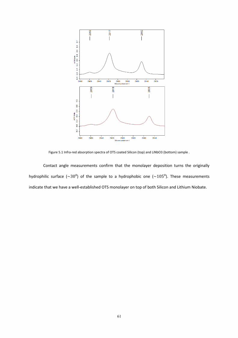
61
Figure 5.1 Infra-red absorption spectra of OTS coated Silicon (top) and LiNbO3 (bottom) sample .
Contact angle measurements confirm that the monolayer deposition turns the originally
hydrophilic surface ( ) of the sample to a hydrophobic one ( ). These measurements
indicate that we have a well-established OTS monolayer on top of both Silicon and Lithium Niobate.
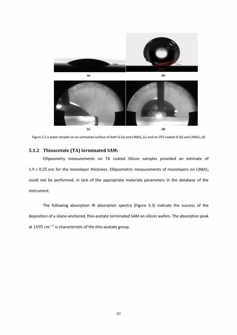
62
Figure 5.2 a water droplet on an untreated surface of both Si (a) and LiNbO3 (c) and on OTS coated Si (b) and LiNbO3 (d)
5.1.2 Thioacetate (TA) terminated SAM:
Ellipsometry measurements on TA coated Silicon samples provided an estimate of
for the monolayer thickness. Ellipsometric measurements of monolayers on LiNbO3
could not be performed, in lack of the appropriate materials parameters in the database of the
instrument.
The following absorption IR absorption spectra (Figure 5.3) indicate the success of the
deposition of a silane-anchored, thio-acetate terminated SAM on silicon wafers. The absorption peak
at is characteristic of the thio-acetate group.
(a) (b)
(c) (d)
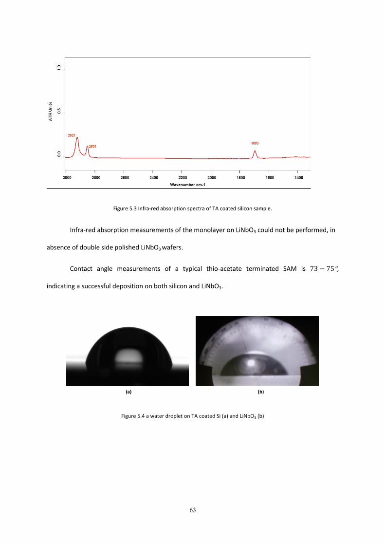
63
Figure 5.3 Infra-red absorption spectra of TA coated silicon sample.
Infra-red absorption measurements of the monolayer on LiNbO3 could not be performed, in
absence of double side polished LiNbO3 wafers.
Contact angle measurements of a typical thio-acetate terminated SAM is ,
indicating a successful deposition on both silicon and LiNbO3.
Figure 5.4 a water droplet on TA coated Si (a) and LiNbO3 (b)
(a) (b)
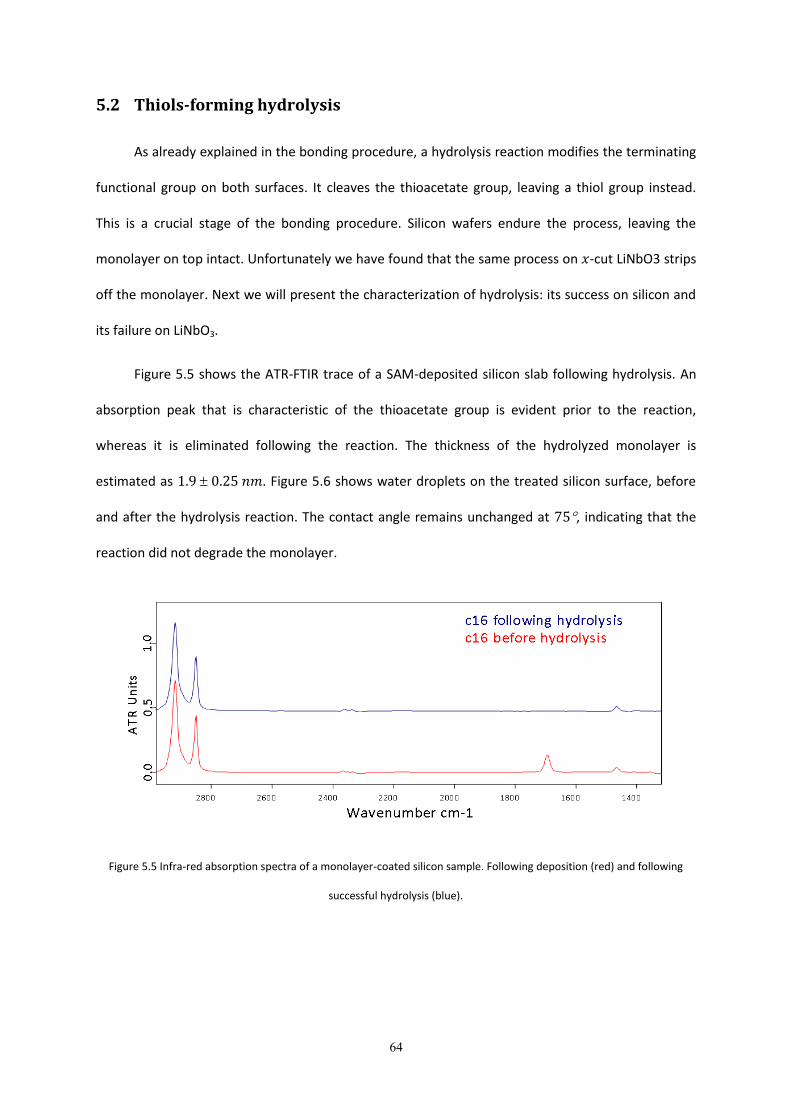
64
5.2 Thiols-forming hydrolysis
As already explained in the bonding procedure, a hydrolysis reaction modifies the terminating
functional group on both surfaces. It cleaves the thioacetate group, leaving a thiol group instead.
This is a crucial stage of the bonding procedure. Silicon wafers endure the process, leaving the
monolayer on top intact. Unfortunately we have found that the same process on -cut LiNbO3 strips
off the monolayer. Next we will present the characterization of hydrolysis: its success on silicon and
its failure on LiNbO3.
Figure 5.5 shows the ATR-FTIR trace of a SAM-deposited silicon slab following hydrolysis. An
absorption peak that is characteristic of the thioacetate group is evident prior to the reaction,
whereas it is eliminated following the reaction. The thickness of the hydrolyzed monolayer is
estimated as . Figure 5.6 shows water droplets on the treated silicon surface, before
and after the hydrolysis reaction. The contact angle remains unchanged at , indicating that the
reaction did not degrade the monolayer.
Figure 5.5 Infra-red absorption spectra of a monolayer-coated silicon sample. Following deposition (red) and following
successful hydrolysis (blue).
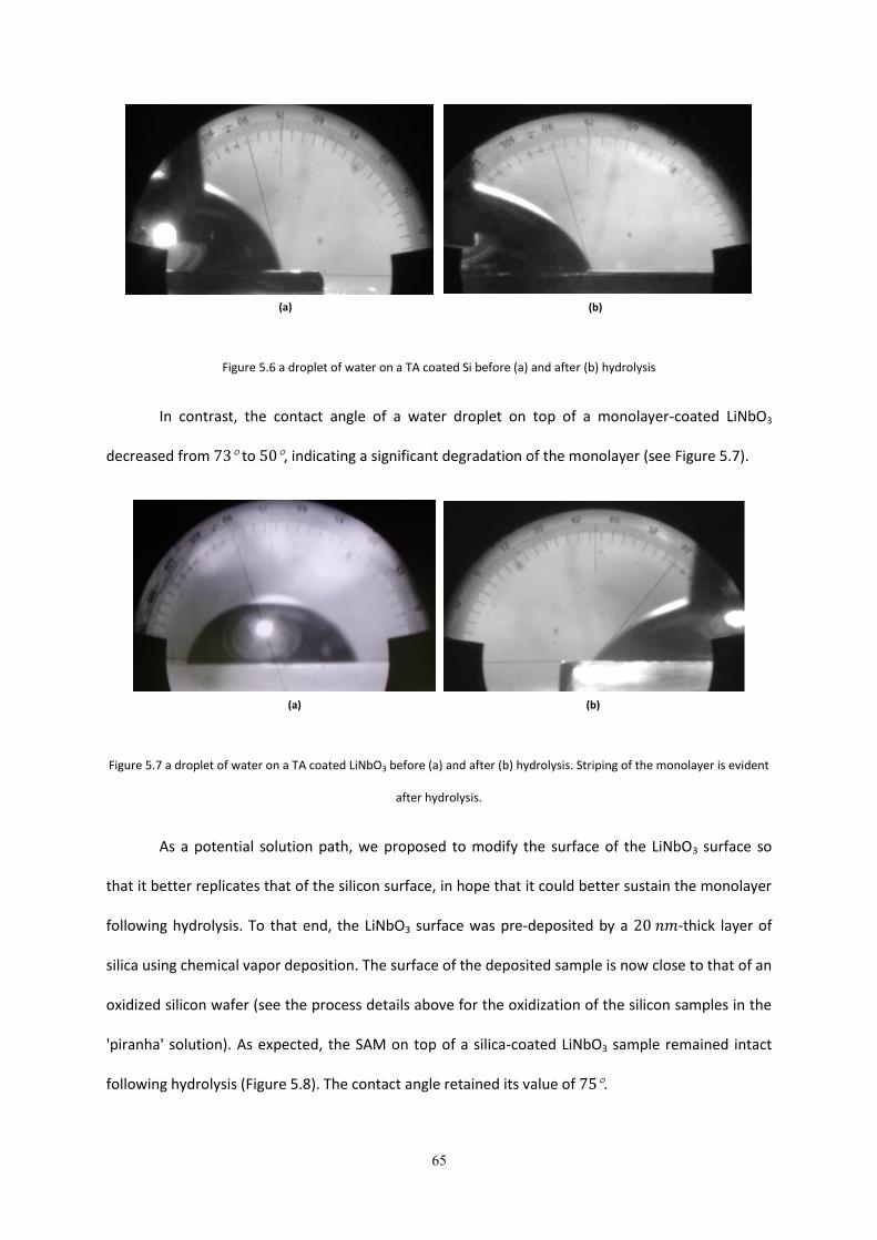
65
Figure 5.6 a droplet of water on a TA coated Si before (a) and after (b) hydrolysis
In contrast, the contact angle of a water droplet on top of a monolayer-coated LiNbO3
decreased from to , indicating a significant degradation of the monolayer (see Figure 5.7).
Figure 5.7 a droplet of water on a TA coated LiNbO3 before (a) and after (b) hydrolysis. Striping of the monolayer is evident
after hydrolysis.
As a potential solution path, we proposed to modify the surface of the LiNbO3 surface so
that it better replicates that of the silicon surface, in hope that it could better sustain the monolayer
following hydrolysis. To that end, the LiNbO3 surface was pre-deposited by a -thick layer of
silica using chemical vapor deposition. The surface of the deposited sample is now close to that of an
oxidized silicon wafer (see the process details above for the oxidization of the silicon samples in the
'piranha' solution). As expected, the SAM on top of a silica-coated LiNbO3 sample remained intact
following hydrolysis (Figure 5.8). The contact angle retained its value of .
(a) (b)
(a) (b)
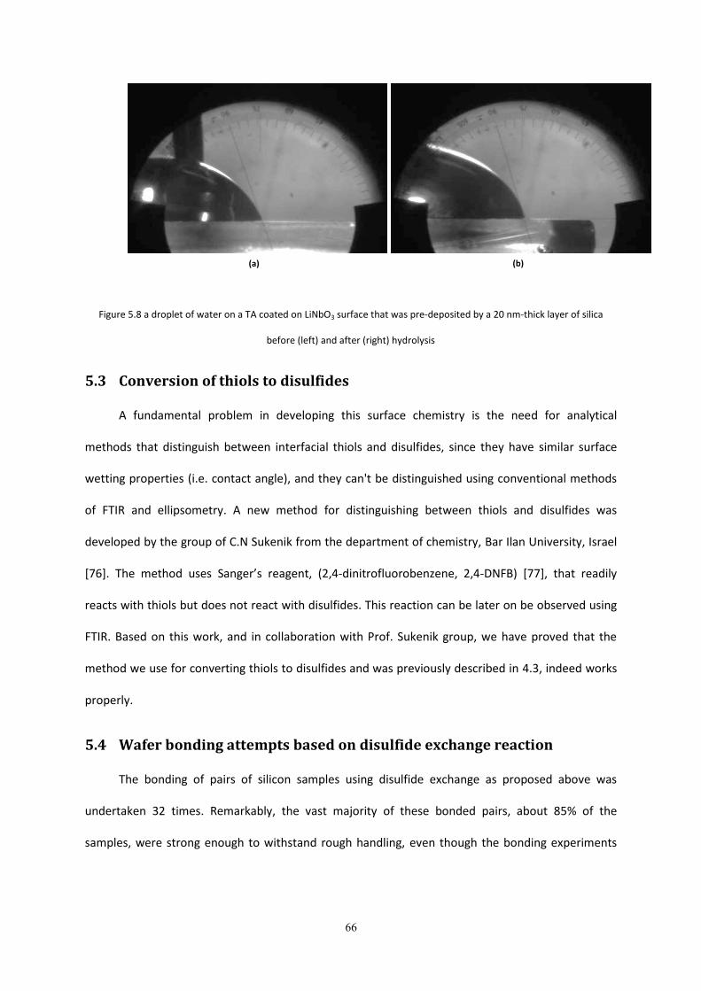
66
Figure 5.8 a droplet of water on a TA coated on LiNbO3 surface that was pre-deposited by a 20 nm-thick layer of silica
before (left) and after (right) hydrolysis
5.3 Conversion of thiols to disulfides
A fundamental problem in developing this surface chemistry is the need for analytical
methods that distinguish between interfacial thiols and disulfides, since they have similar surface
wetting properties (i.e. contact angle), and they can't be distinguished using conventional methods
of FTIR and ellipsometry. A new method for distinguishing between thiols and disulfides was
developed by the group of C.N Sukenik from the department of chemistry, Bar Ilan University, Israel
[76]. The method uses Sanger’s reagent, (2,4-dinitrofluorobenzene, 2,4-DNFB) [77], that readily
reacts with thiols but does not react with disulfides. This reaction can be later on be observed using
FTIR. Based on this work, and in collaboration with Prof. Sukenik group, we have proved that the
method we use for converting thiols to disulfides and was previously described in 4.3, indeed works
properly.
5.4 Wafer bonding attempts based on disulfide exchange reaction
The bonding of pairs of silicon samples using disulfide exchange as proposed above was
undertaken 32 times. Remarkably, the vast majority of these bonded pairs, about 85% of the
samples, were strong enough to withstand rough handling, even though the bonding experiments
(a) (b)
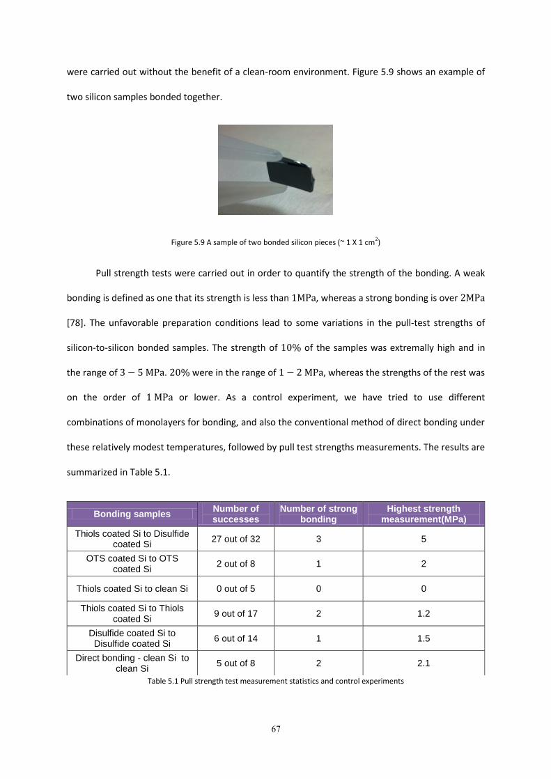
67
were carried out without the benefit of a clean-room environment. Figure 5.9 shows an example of
two silicon samples bonded together.
Figure 5.9 A sample of two bonded silicon pieces (~ 1 X 1 cm2)
Pull strength tests were carried out in order to quantify the strength of the bonding. A weak
bonding is defined as one that its strength is less than , whereas a strong bonding is over
[78]. The unfavorable preparation conditions lead to some variations in the pull-test strengths of
silicon-to-silicon bonded samples. The strength of of the samples was extremally high and in
the range of . were in the range of , whereas the strengths of the rest was
on the order of or lower. As a control experiment, we have tried to use different
combinations of monolayers for bonding, and also the conventional method of direct bonding under
these relatively modest temperatures, followed by pull test strengths measurements. The results are
summarized in Table 5.1.
Table 5.1 Pull strength test measurement statistics and control experiments
Bonding samples Number of successes
Number of strong bonding
Highest strength measurement(MPa)
Thiols coated Si to Disulfide coated Si
27 out of 32 3 5
OTS coated Si to OTS coated Si
2 out of 8 1 2
Thiols coated Si to clean Si 0 out of 5 0 0
Thiols coated Si to Thiols coated Si
9 out of 17 2 1.2
Disulfide coated Si to Disulfide coated Si
6 out of 14 1 1.5
Direct bonding - clean Si to clean Si
5 out of 8 2 2.1
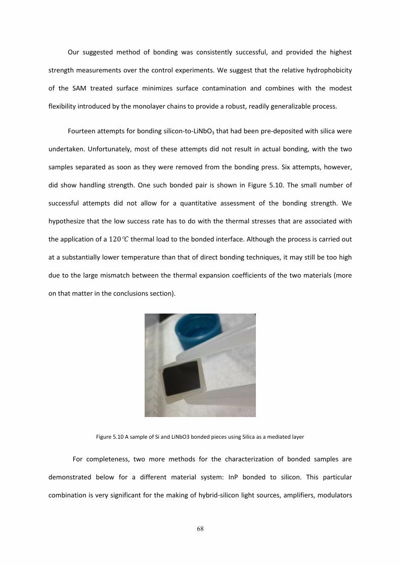
68
Our suggested method of bonding was consistently successful, and provided the highest
strength measurements over the control experiments. We suggest that the relative hydrophobicity
of the SAM treated surface minimizes surface contamination and combines with the modest
flexibility introduced by the monolayer chains to provide a robust, readily generalizable process.
Fourteen attempts for bonding silicon-to-LiNbO3 that had been pre-deposited with silica were
undertaken. Unfortunately, most of these attempts did not result in actual bonding, with the two
samples separated as soon as they were removed from the bonding press. Six attempts, however,
did show handling strength. One such bonded pair is shown in Figure 5.10. The small number of
successful attempts did not allow for a quantitative assessment of the bonding strength. We
hypothesize that the low success rate has to do with the thermal stresses that are associated with
the application of a thermal load to the bonded interface. Although the process is carried out
at a substantially lower temperature than that of direct bonding techniques, it may still be too high
due to the large mismatch between the thermal expansion coefficients of the two materials (more
on that matter in the conclusions section).
Figure 5.10 A sample of Si and LiNbO3 bonded pieces using Silica as a mediated layer
For completeness, two more methods for the characterization of bonded samples are
demonstrated below for a different material system: InP bonded to silicon. This particular
combination is very significant for the making of hybrid-silicon light sources, amplifiers, modulators
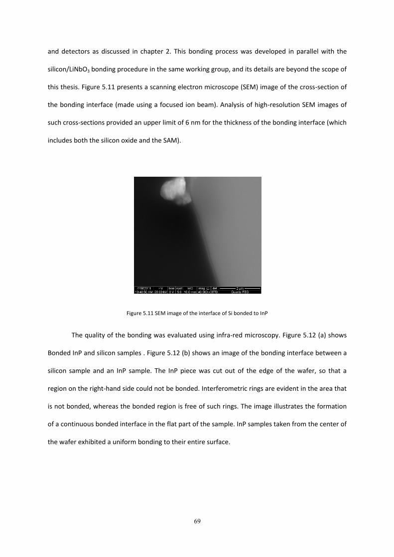
69
and detectors as discussed in chapter 2. This bonding process was developed in parallel with the
silicon/LiNbO3 bonding procedure in the same working group, and its details are beyond the scope of
this thesis. Figure 5.11 presents a scanning electron microscope (SEM) image of the cross-section of
the bonding interface (made using a focused ion beam). Analysis of high-resolution SEM images of
such cross-sections provided an upper limit of 6 nm for the thickness of the bonding interface (which
includes both the silicon oxide and the SAM).
Figure 5.11 SEM image of the interface of Si bonded to InP
The quality of the bonding was evaluated using infra-red microscopy. Figure 5.12 (a) shows
Bonded InP and silicon samples . Figure 5.12 (b) shows an image of the bonding interface between a
silicon sample and an InP sample. The InP piece was cut out of the edge of the wafer, so that a
region on the right-hand side could not be bonded. Interferometric rings are evident in the area that
is not bonded, whereas the bonded region is free of such rings. The image illustrates the formation
of a continuous bonded interface in the flat part of the sample. InP samples taken from the center of
the wafer exhibited a uniform bonding to their entire surface.
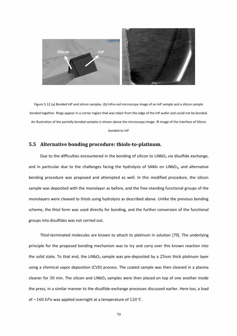
71
Figure 5.12 (a) Bonded InP and silicon samples. (b) Infra-red microscopy image of an InP sample and a silicon sample
bonded together. Rings appear in a corner region that was taken from the edge of the InP wafer and could not be bonded.
An illustration of the partially bonded samples is shown above the microscopy image. IR image of the interface of Silicon
bonded to InP
5.5 Alternative bonding procedure: thiols-to-platinum.
Due to the difficulties encountered in the bonding of silicon to LiNbO3 via disulfide exchange,
and in particular due to the challenges facing the hydrolysis of SAMs on LiNbO3, and alternative
bending procedure was proposed and attempted as well. In this modified procedure, the silicon
sample was deposited with the monolayer as before, and the free-standing functional groups of the
monolayers were cleaved to thiols using hydrolysis as described above. Unlike the previous bonding
scheme, the thiol form was used directly for bonding, and the further conversion of the functional
groups into disulfides was not carried out.
Thiol-terminated molecules are known to attach to platinum in solution [79]. The underlying
principle for the proposed bonding mechanism was to try and carry over this known reaction into
the solid state. To that end, the LiNbO3 sample was pre-deposited by a thick platinum layer
using a chemical vapor deposition (CVD) process. The coated sample was then cleaned in a plasma
cleaner for min. The silicon and LiNbO3 samples were then placed on top of one another inside
the press, in a similar manner to the disulfide-exchange processes discussed earlier. Here too, a load
of was applied overnight at a temperature of .
Silicon InP
Silicon
InP
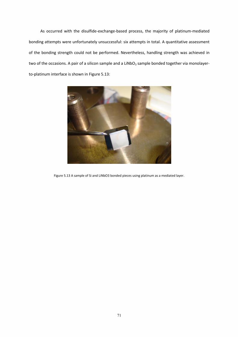
71
As occurred with the disulfide-exchange-based process, the majority of platinum-mediated
bonding attempts were unfortunately unsuccessful: six attempts in total. A quantitative assessment
of the bonding strength could not be performed. Nevertheless, handling strength was achieved in
two of the occasions. A pair of a silicon sample and a LiNbO3 sample bonded together via monolayer-
to-platinum interface is shown in Figure 5.13:
Figure 5.13 A sample of Si and LiNbO3 bonded pieces using platinum as a mediated layer.
72
6. Summary and Conclusions
In this work, I have presented a technology for the vertical integration between LiNbO3 and
of silicon-on-insulator (SOI) substrates, for the future fabrication of integrated hybrid electro-optic
modulators. Thus type of hybrid-silicon photonics is of major potential importance and interest,
since although silicon is the material of choice for the mature and developed electronic integrated
circuits industry, realization of modulators and other active devices in silicon is difficult. The two
specific objectives of my work over the last two years were the following key aspects of such
devices: The geometric design and the bonding technology.
On the design part, our analysis and simulations suggested that hybrid silicon-LiNbO3
modulators should be feasible, with a product that is on the same order of magnitude as that of
stand-alone LiNbO3 modulators. Two designs were discussed: 1) a far spaced electrode
configuration, which is easier to fabricate but requires high voltages, and should serve for a proof-of-
principle; and 2) a more advanced device with closely spaced electrodes.
On the bonding parts we proposed a new bonding paradigm of SAM-assisted bonding. The
advantage of this method is the usage of a relatively low temperature of 120⁰C. It potentially
reduces the thermal stresses that stem from the mismatch between the thermal expansion
coefficients of silicon and LiNbO3. Our process relies on the deposition of SAMs of organic material
on either one or both surfaces to be bonded, and their subsequent functionalization using specific
chemical reactions which allow for the bonding of the two surfaces at low temperatures. The wafer
bonding procedure was addressed in detail and the chemical processes were described. During the
development of the process, I became familiar not only with the area of SAM, but also with many
fabrication procedures and analytic and characterization tools such as AFM, FTIR, contact angle
measurements, SEM, IR imaging and pull strength tests.
The bonding of silicon-to-silicon was successful, while the application of the process to the
bonding of silicon to LiNbO3 faced difficulties, such as the stripping of the monolayer on LiNbO3
73
pieces after the hydrolysis reaction. As a potential solution path, we modified the surface of the
LiNbO3 so that it better replicates that of the silicon surface, and used LiNbO3 that had been pre-
deposited with silica. A bonding of silicon-to-LiNbO3 that had been pre-deposited with silica was
attempted a number of times. Most of these attempts did not result in actual bonding, and only
showed handling strength when removed from the bonding press. A second variant of the process,
using platinum coated LiNbO3, also showed limited success to-date.
We hypothesize that the low success rate has to do with the thermal stresses that are
associated with the application of a 120 ⁰C thermal load to the bonded interface. Although the
process is carried out at a substantially lower temperature than that of direct bonding techniques, it
may still be too high due to the large mismatch between the thermal expansion coefficients of the
two materials. LiNbO3 and Silicon expend differently under 120 ⁰C. The bonding occurs after a few
hours when the two surfaces have reached this temperature, and each had expended accordingly.
When taken out of the bonding press, the samples are cooled down to room temperature, and each
of the materials contract back. If a bonding has occurred, the molecules that bond the two surfaces
may be torn away because of these thermal stresses leading to bonding failure. In addition, the lack
of clean room environment may also be a cause to the failure of bonding attempts.
Future work could see an improvement in bonding success, first and foremost, through
working in cleanroom environments that are now becoming available to us. In addition, alternative
bonding procedures, which may take place at room temperature or close to it, could be attempted.
These include different types of monolayer based reactions, direct bonding via oxygen plasma
activation, or the electro-static attraction between polymer chains of opposite charge [80,81].
In summary, the goal of generating a hybrid silicon-LiNbO3 electro-optic modulator is still a
notable one with great potential importance. Furthermore, the concept of SAM-assisted bonding is
worth pursuing from the fundamental material science standpoint as well. I expect considerable
progress towards that objective in the next few years.
74
References
[1] L. Pavesi, “Will Silicon Be the Photonic Material of the Third Millenium?,” Journal of Physics 15,
1169–1196 (2003).
[2] G.Reed, Silicon Pohtonics: the state of the art, pp. 1–13, John Wiley &Sons (2008).
[3] R. A. Soref and B. R. Bennett., “Electrooptical effects in silicon,” Journal Quantum Electronics, IEEE
23, 123–129 (1987).
[4] W. R. Boyd, Nonlinear Optics, 3rd ed., pp. 207–251, Academic Press (2008).
[5] E. L. Wooten, K. M. Kissa, A. Yi-Yan, E. J. Murphy, D. A. Lafaw, D. Maack, D. V. Attanasio, D. J.
Fritz, G. J. McBrien, et al., “A Review of Lithium Niobate Modulators for Fiber-Optic Communications
Systems,” Journal Quantum Electronics, IEEE 6, 69–82 (2000).
[6] T. Chassé and D. Zerulla, “Structure and self-assembly of alkanethiols on III–V semiconductor
surfaces,” Journal of Electron Spectroscopy and Related Phenomenal 172, 78–87 (2009).
[7] H. Yamamoto, R. A. Butera, Y. Gu, and D. H. Waldeck, “Characterization of the Surface to Thiol
Bonding in Self-Assembled Monolayer Films of C12H25SH on InP by Angle-Resolved X-ray
Photoelectron Spectroscopy,” Langmuir 15, 8640–8644 (1999).
[8] Y. B. Park, B. Min, K. J. Vahala, and H. Atwater, “Integration of Single-Crystal LiNbO3 Thin Film on
Silicon by Laser Irradiation and Ion Implantation–Induced Layer Transfer,” Advanced Materials 18,
1533–1536 (2006).
[9] K. Diest, M. J. Archer, J. A. Dionne, Y. B. Park, M. J. Czubakowski, H. A. Atwater, and T. J. Watson,
“Silver diffusion bonding and layer transfer of Lithium Niobate to silicon,” Applied Physics Letters 93,
93–96 (2008).
[10] Y. Lee, W. G. Lee, and W. Steier, “Fabrication of free standing LiNbO3 single crystal micro-platelets
and their integration to Si-on-insulator platforms,” Thin Solid Films 519, 4271–4276 (2011).
[11] M. M. R. Howladera, T. Suga, and M. J. Kim, “Room temperature bonding of silicon and Lithium
Niobate,” Advanced Materials 18, 1533–1536 (2006).
[12] H.Takagi, R. Maeda, and T. Suga, “Room-temperature wafer bonding of Si to LiNbO3, LiTaO3 and
Gd3Ga5O12 by Ar-beam surface activation,” Journal of Micromechanics and Microengineering 11,
348–352 (2001).
[13] Y. S. Lee, G. duk Kim, W. ju Kim, S. shin Lee, W. gyu Lee, and W. H. Steier, “Hybrid Si-LiNbO3
microring electro-optically tunable resonators for active photonic devices,” Optics Letters 36, 1119–
1121 (2011).
[14] H. Takagi, R. Maeda, N. Hosoda, and T. Suga, “Room-temperature wafer bonding of Si to LiNbO3,
LiTaO3 and Gd3Ga5O12 by Ar-beam surface activation,” Applied Physics Letters 74, 2387–2389
(1999).
[15] B. Jalali, “Teaching silicon new tricks,” Nature Photonics 1, 193–195 (2007).
[16] S. Fathpour and B. Jalali, “Silicon Photonics,” Journal of Lightwave Technology 24, 4600–4615 (2006).
[17] P. Yeh and A. Yariv, “Photonics: optical electronics in modern communication,” Oxford Uni. Press
(2007).
75
[18] G. Agrawal, “Nonlinear Fiber Optics,” Elvsevier – Academic Press (2007).
[19] B. W. Robert, “Nonlinear Optics,” Academic Press (2008).
[20] G. Reed and A. Knights, Silicon Photonics: an introduction, pp. 165–167, John Wiley &Sons (2004).
[21] A. Zadok, Electro-Optic Systems for Signal Processing, Lecture Notes, Bar Ilan Uni. Israel (2010).
[22] W. Bogaerts, P. Dumon, D. V. Thourhout, D. Taillaert, P. Jaenen, J. Wouters, S. Beckx, V. Wiaux, and
R. G. Baets, “Compact Wavelength-Selective Functions in Silicon-on-Insulator Photonic Wires,” IEEE
J. of Selected Topics in Quantum Electronics 12, 1394–1401 (2006).
[23] C. E. Peng and G. T. Reed, “Silicon Optical Modulators,” Materials Today 8, 40–50 (2005).
[24] Y. H. Kuo, H. W. Chen, and J. E. Bowers, “High speed hybrid silicon evanescent electroabsorption
modulator,” Optics express 16, 9936–9941 (2008).
[25] A. P. Jauho and K. Johnsen, “Dynamical Franz-Keldysh effect,” physics review letters 33, 3976–6982
(1995).
[26] M. Leroux, N. Grandjean, M. Laugt, and J. Massies, “Quantum confined Stark effect due to built-in
internal polarization fields in (Al,Ga) N/GaN quantum wells,” Physical Reveiew B 58, 371–374 (1998).
[27] H. Park, Y.-H. Kuo, A. W. Fang, R. Jones, O. Cohen, M. J. Paniccia, and J. E. Bowers, “A hybrid
AlGaInAs-silicon evanescent preamplifier and photodetector.,” Optics express 15, 13539–13546 (2007).
[28] W. R. Boyd, Nonlinear Optics, 3rd ed., Elvsevier – Academic Press (2008).
[29] P. Yeh and A. Yariv, Photonics: optical electronics in modern communication, 6th ed., pp. 406–418,
Oxford Uni. Press (2007).
[30] C. K. Tang and G. T. Reed, “Highly efficient optical phase modulator in SOI,” waveguides Electron
Letters 31, 451–452 (1995).
[31] A. Liu, R. Jones, L. Liao, and D. Samara-rubio, “A high speed silicon optical modulator based on a
metal oxide semiconductor capacitor,” letters to nature 427, 615–618 (2004).
[32] Q. Xu, B. Schmidt, S.Pradhan, and M.Lipson, “Micrometre-scale silicon electro-optic modulator,”
Nature 435, 325–327 (2005).
[33] W. M. J. Green, M. J. Rooks, L.Sekaric, and Y. A. Vlasov, “Ultra-compact, low RF power, 10 Gb/s
silicon Mach-Zehnder modulator,” Optics Express 15, 17106–17113 (2007).
[34] D. J. Thomson, F. Y. Gardes, J. M. Fedeli, S. Zlatanovic, Y. Hu, P. P. Kuo, N. Alic, S. Radic, G. Z.
Mashanovich, et al., “High data rate silicon optical modulator with self-aligned fabrication process,”
OFC 2012 Conference, Convention centre, LA.
[35] A. W. Fang, H. Park, O. Cohen, R. Jones, M. J. Paniccia, and J. E. Bowers, “Electrically pumped hybrid
AlGaInAs-silicon evanescent laser.,” Optics express 14, 9203–9210 (2006).
[36] J. W. Aring, E. J. Skogen, L. A. Johansson, M. N. Sysak, J. S. Barton, M. L. Ma, and L. A. Coldren,
“Demonstration of Widely Tunable Single-Chip 10-Gb/s Laser – Modulators Using Multiple-Bandgap
InGaAsP Quantum Well Intermixing,” IEEE Photonics Technology Letters 16, 1613–1615 (2004).
[37] J. Shirinizu, M. Aoki, T. Tsucjiya, M. Shirai, A. Taike, T. Ohtoshi, and S. Tsuji, “Advantages of Optical
modulators with InGaAlAs/InGaAlAs MQW structure,” Elecronic Letters 38, 821–822 (2002).
76
[38] Y. Tang, J. D. Peters, and J. E. Bowers, “Over 67 GHz bandwidth hybrid silicon electroabsorption
modulator with asymmetric segmented electrode for 1.3 μm transmission.,” Optics express 20, 11529–
11535 (2012).
[39] M. J. R. Heck, H. wen Chen, A. W. Fang, B. R. Koch, D. Liang, H. Park, M. N. Sysak, and J. E.
Bowers, “Hybrid Silicon Photonics for Optical Interconnects,” IEEE Journal of Selected Topics in
Quantum Electronics 260, 1077–1091 (2010).
[40] H. wen Chen, Y. hao Kuo, and J. E. Bowers, “Hybrid silicon evanescent phase modulator based on
carrier depletion in offset multiple-quantum-well,” Conference on Lasers and Electro-Optics, 1–2, Ieee
(2008).
[41] O. Zucker, W. Langheinrich, and M. Kulozik, “Application of oxygen plasma processing to silicon
direct bonding,” Sensors and Actuators A: Physical 36, 227–231 (1993).
[42] D. Pasquariello, C. Hedlund, and K. Hjort, “AIGaN/GaN hetrostructure field effect transistoe fabricated
on 100mm Si/Poly SiC composite substrates,” Journal Electrochemistry society 147, 2699 (2000).
[43] R. S. Weis and T. K. Gaylord, “Lithium Niobate: Summary of Physical Properties and Crystal
Structure,” Applied Physics A 37, 191–203 (1985).
[44] S. Sanna and W. G. Schmidt, “Lithium niobate X-cut, Y-cut, and Z-cut surfaces from ab initio theory,”
Physical Review B 81, 1–11 (2010).
[45] G. Boyd, W. Bond, and H. Carter, “Refractive Index as a Function of Temperature in LiNbO3,” Journal
of Applied Physics 38, 1941–1945 (1967).
[46] S. Kielich, “Nonlinear optical and electro-optical properties of dielectrics and ferroelectrics,”
Ferroelectrics 4, 257–282 (1972).
[47] J. Witzens, T. Baehr-Jones, and M. Hochberg, “Design of transmission line driven slot waveguide
Mach-Zehnder interferometers and application to analog optical links,” Optics express 18, 16902–16928
(2010).
[48] S. Onclin, B. J. Ravoo, and D. N. Reinhoudt, “Engineering silicon oxide surfaces using self-assembled
monolayers.,” Angewandte Chemie 44, 6282–6304 (2005).
[49] J. J. Shyue, M. D. Guire, T. Nakanishi, Y. Masuda, K. Koumoto, and C. N. Sukenik, “Acid-Base
Properties and Zeta Potentials of Self-Assembled Monolayers Obtained via in Situ Transformations,”
Langmuir 20, 8693–8698 (2004).
[50] J. Sagiv, “A new approach to construction of artificial monolayer assemblies,” Journal American
Chemical Society 102, 92 (1983).
[51] R. G. Nuzzo and D. Allara, “Adsorption of Bifunctional Organic Disulfides on Gold Surfaces,” Journal
American Chemical Society 105, 4481 (1983).
[52] M. C. Pirrung, “How to make a DNA chip,” Angewandte Chemie 41, 1276–1289 (2002).
[53] D. S. Wilson and S. Nock, “Recent developments in protein microarray technology.,” Angewandte
Chemie 42, 494–500 (2003).
[54] A. W. Adamson, “Physical Chemistry of Surfaces,” Wiley: New York (1976).
[55] R. W. Murray, “Chemically Modified Electrodes,” Accounts of Chemistry Research 117, 135–141
(1980).
77
[56] J. R. Mohrig, C. Hammond Noring, and P. F. Schatz, “Techniques of Organic Chemistry,” Wiley: New
York (2006).
[57] F. Kajzar and J. Messier, “Nonlinear Interferometry in Langmuir-Blodgett multylayers of
Polydiacetylene,” Optics Communication 45, 133–137 (1983).
[58] G. Kräuter, Y. Bluhm, C. Batz-Sohn, and U. Gösele, “The Joining of Parallel Plates via Organic
Monolayers: Chemical Reactions in a Spatially Confined System,” Advanced Materials 11, 1035
(1999).
[59] W. Ashurst, C. Yau, C. Carraro, R. Maboudian, and M. Dugger, “Dichlorodimethylsilane as an Anti-
Stiction Monolayer for MEMS: A Comparison to the Octadecyltrichlosilane Self-Assembled
Monolayer,” Jornal of Microelectromechanical systems 20, 41–49 (2001).
[60] V. DePalma and N. Tillman, “Friction and Wear of Self -Assembled Trichlorosilane Monolayer Films
on Silicon,” Langmuir, 868–872 (1989).
[61] M. R. Linford, P. Fenter, P. M. Eisenberger, and C. E. D. Chidsey, “Alkyl Monolayers on Silicon
Prepared from 1-Alkenes and Hydrogen-Terminated Silicon,” Journal of the American Chemical
Society 117, 3145–3155 (1995).
[62] S. Meth and C. N. Sukenik, “iloxane-anchored thin films on silicon dioxide modified stainless steel.
Elsevier Science,” Thin Solid Films 425, 49–58 (2003).
[63] Y. Z. Du, L. L. Wood, and S. S. Saavedra, “Growth behavior and structure of alkyltrichlorosilane
monolayers bearing thioacetate and acetate tailgroups,” Materials Science and Engineering C 7, 161–
169 (2000).
[64] K. E. Yelm, “A simple method for in situ generation of thiols from thioacetates,” Tetrahedron Letters
40, 1101–1102 (1999).
[65] H. F. Gilbert, “Molecular and cellular aspects of thiol-disulfide exchange,” Advances in Enzymology
and Related Areas of Molecular Biology 63, 69–172 (1990).
[66] J. Vickerman and I. Gilmore, Surface Analysis - The Principal Techniques, 2nd ed., p. chapter 7, John
Wiley and Sons (2009).
[67] A. Adamson and A. Gast, Physical Chemistry of Surfaces, pp. 255–361, John Wiley & Sons (1997).
[68] O. Gershevitz and C. N. Sukenik, “In Situ FTIR-ATR Analysis and Titration of Carboxylic Acid-
Terminated SAMs,” Journal American Chemical Society 126, 482–483 (2003).
[69] S. Magonov and M. H. Whangbo, Surface Analysis with STM and AFM: Experimental and Theoretical
Aspects of Image Analysis, pp. 311–344, VCH Publishers (1996).
[70] S. R. Wasserman, G. M. Whitesides, and J. D. Axe, “The structure of self assembled monolayers of
alkyloxanes on silicon: a comparison of results from ellipsometry and low angle X-ray reflectivity,”
Journal American Chemical Society 35, 19–23 (1989).
[71] T. Matthias and V. Dragoi, “Failure mechanisms in wafer bonding. Conference: Design, Test,
Integration and Packing of Mems/Moems. Montreux Switzerland,” Company: EVG (2004).
[72] J. Goldstein, D. Newbury, D. Joy, C. Lyman, P. Echlin, E. Lifshin, L. Sawyer, and J. Michael, Scanning
Electron Microscopy and X-ray Microanalysis, 3rd ed., pp. 21–38, Kluwer Academic/Plenum, New
York (2003).
78
[73] J. Valli, “A review of adhesion test methods for thin hard coatings,” Journal of Vacuum Science &
Technology A 4, 3007–3015 (1986).
[74] R. G. Maev, “Acoustic Microscopy,” Wiley-VCH, Weinheim (2008).
[75] N. Balachander and C. N. Sukenik, “Monolayer transformation by nucleophilic substitution:
Applications to the creation of new monolayer assemblies,” Langmuir 6, 1621 (1990).
[76] V. Artel, I. Aped, R. Cohen, and C. N. Sukenik, “Controlled Formation of Thiol and Disulfide
Interfaces,” submitted for publication.
[77] S. Shaltiel, “Thiolysis of some dinitrophenyl derivatives of amino acids,” Biochemical and Biophysical
Research Communications 29, 178–183 (1967).
[78] M. M. R. Howlader, T. Watanabe, and T. Suga, “Characterization of the bonding strength and interface
current of p-Si/n-InP wafers bonded by surface activated bonding method at room temperature,” Journal
of Applied Physics 91, 3062–3067 (2002).
[79] A.Ulman, An Introduction to Ultrathin Organic Films: From Langmuir–Blodgett to Self-assembly,
Academic Press (1988).
[80] W. Chen and T. J. Mccarthy, “Layer-by-Layer Deposition: a Tool for Polymer Surface Modification,”
Macromolecules 30, 78–86 (1997).
[81] K. Ariga, J. P. Hill, and Q. Ji, “Layer-by-layer assembly as a versatile bottom-up nanofabrication
technique for exploratory research and realistic application.,” Physical chemistry chemical physics 9,
2319–2340 (2007).


תקציר:
, זהעל פני מרחקים ארוכיםהעברת מידע בנפח רב כמעט בלעדי להאמצעי ה הינהתקשורת אופטית
והדרישה להעלאת קצב שיתוף המידע נתונים האחסון תכמובעידן המודרני, ככל שלמעלה משלושה עשורים.
צמיחה אל רמת הלוח, השבב ואף המעבד. אופטיקה חודרות בהדרגה-תקשורת מבוססות, טכנולוגיות גדלים
ת ומערכ של אפקטיביתאינטגרציה ב, במידה רבה, התלוי של תחומי התקשורת והמחשוב גם יחדעתידית
פלטפורמת סיליקון. לפיכך, מימוש של התקנים גבי על משולבים, אלקטרוניים מעגלים לצדתקשורת אופטית
רבה.בעל חשיבות סיליקון הוא תחום מחקר גבי-פוטוניים על
למימושבדרך כלל מוצלחתמהווה פלטפורמה (SOIמבודד ) גבי-סיליקון עלמערכת החומרים של בעוד
ם מאפנני כדוגמתרכיבים אקטיביים יישום ומהודים, אינטרפרומטריםמוליכי גלים, כגוןפסיביים רכיבים
יישום בפני מספר אתגרים מציבותהתכונות הבסיסיות של הסיליקון גבי סיליקון מורכב יותר.-ומקורות אור על
זהאפקט מסדר שני. אלקטרו אופטיה אפקטשל ה הוא היעדר כזה חסרון אחד אקטיביים.התקנים פוטוניים
של מאפננים פעולתםהעומד בבסיס מנגנון פעלת מתח חיצוני,כתוצאה מה מקדם השבירה שינוי על אחראי
. אופטיות ברשתות תקשורת מרכיבים מרכזייםשהם , אופטיים-אלקטרו
אופטי -מקדם אלקטרולחומר . LiNbO3)מאפננים שכאלו הוא ניתיום ניאובט ) למימוש הנפוץ ביותרהחומר
קיים עניין רב לפיכך מפותחת ומבוססת היטב. ליתיום ניאובטמודולטורים מבוססי של יצור ה תויטכנולוגו ,גבוה
התזה .בהיבטים מחקריים ומסחריים גם יחד ,אחד התקןב סיליקון לצד ליתיום ניאובט של היברידישילוב ב
אופטי משולב הבנוי בטכנולוגיה -קטרו, שמטרתו לייצר מודולטור אלהיא חלק ממחקר ארוך טווח המוצגת להלן
שתי משימות מרכזיות במהלך המחקר התמודדתי עם בסיליקון. יםיתיום ניאובט מעל מוליך גלהיברידית של ל
והתכנון הגיאומטרי של ההתקן ההיברידי. ,סיליקוןבין החיבור בין ליתיום ניאובט לאופן : לקראת יעד זה
או הדבקה "direct bonding"השיטה הרווחת ביותר כיום לחיבור חומרים אלקטרו אופטיים שונים נקראת
שניפני השטח של קפדני של ניקיון ביניים כלשהן, והיא מבוססת עלשכבות ישירה. השיטה אינה מצריכה
מעלות צלזיוס. השיטה 033-033תוך הפעלת לחץ וטמפרטורה של זה לזההצמדתם וחלקים, מצעים
, אך אינה מתאימה סיליקון, לדוגמה( וInPפוספיד )-מיושמת בהצלחה ביצור רכיבים היברידיים של אינדיום
שונים, דבר ( של שני החומריםCTEמאחר ומקדמי ההתפשטות התרמי ) סיליקוןו לחיבור ליתיום ניאובט

חיבור הינהשיטה נוספת בעת ניסיון החיבור. הממשק שבין החומריםעל קיצוניים תרמיים יוצר מאמציםה
את מעבר האור בין ועלולה לשבש באמצעות שכבת ביניים של פולימר, אך השכבה הנ"ל עבה יחסית
לסיליקון.הדבקה בין ליתיום ניאובט לבספרות אזכורים מעטים בלבד קיימים השכבות. כתוצאה מכך,
אשר ,ריתמולקול-יצירת שכבה חדסתמכת על חלק עיקרי מהתזה מוקדש לפיתוח שיטת חיבור חדשה שמ
לאחר . משטחיםהשני ( על פני "Self-assembled monolayers") מתהווה באופן ספונטני מתוך תמיסה
הדבקה של שני מתאפשרתבאמצעות תגובות כימיות ספציפיות, הפעלה של השכבה החד מולקולרית
ההדבקה תהליכי יצירת השכבות, התגובות הכימיות הנלוות ותהליכי משטחים בטמפרטורות נמוכות.
הוא על פני השיטות הקיימות, המוצעתשיטה . היתרון העיקרי של הבגוף העבודה בפרוטרוט מתוארים
פני -אשר מפחית את המאמצים התרמיים הנוצרים על מעלות 023טמפרטורה נמוכה יחסית של השימוש ב
.ממשק ההדבקה
מרחק רב בין ראשונה בחשבון, כאשר בות של הרכיב נלקחו תכנון הגיאומטרי, שתי תצורבחלק המוקדש ל
קלה יותר למימוש אך דורשת הפעלת מתחים גבוהים זומאות מיקרונים. תצורה , מסדר גודל של האלקטרודות
ומבוססת על מרחק של מיקרונים בודדים בין יותר מורכבתיה י. התצורה השנקצבים נמוכיםומתאימה ל
,אפשרי בילים למסקנה כי מימוש מודולטורים היברידיים הינומוניתוחים המתמטיים האלקטרודות. סימולציות ו
קיימים מבוססי ליתיום מודולטורים דומה לזה של מסדר גודל והם עשויים להתאפיין במימדים ומתחי הפעלה
. ניאובט
חיבור ליתיום , ראשוניות הצלחותמצומצם של למרות מספר תוצאות ההדבקה.ב עוסק תזהב האחרוןהפרק
להחזיק את זמנית יכולת בניאובט וסיליקון נתקל בקשיים ומרבית הניסיונות לא הסתיימו בחיבור ממש אלא רק
פתרונות . הלא אידאלייםהכנה האנו מייחסים את הקשיים הללו בעיקר לתנאי הדגימות מחוברות באוויר.
שינויים בשיטה כי לאחר שיבוצעו מספראנו מקווים . נידונים בסיום העבודהאפשריים לשיפור ההדבקה
נוכל לייצור מודולטורים היברידיים של ליתיום ניאובט וסיליקון.הקיימת,

מהפקולטה ד"ר אבי צדוקהמחקר לתזה בוצע תחת הנחייתו של
אילן-להנדסה באוניברסיטת בר

בסיליקון וליתיום מודולטור אלקטרואופטי היברידי
ניאובט: תכנון גיאומטרי וטכניקות להדבקה בין מצעים
אילוביץ טלי
עבודה זו מוגשת כחלק מהדרישות לשם קבלת תואר מוסמך
אילן-של אוניברסיטת ברפקולטה להנדסה ב
תשע"באלול רמת גן
