i layout design and simulation of complementary...
TRANSCRIPT

i
LAYOUT DESIGN AND SIMULATION OF COMPLEMENTARY METAL –
OXIDE – SEMICONDUCTOR (CMOS) OPERATION AMPLIFIER
FAUZIAH BINTI OSMAN
A thesis submitted in partial fulfillment of the requirements for the award of the
degree of Bachelor of Electronic Engineering (Computer Engineering)
Faculty of Electronic and Computer Engineering
Universiti Teknikal Malaysia Melaka (UTeM)
MAY 2011
ii
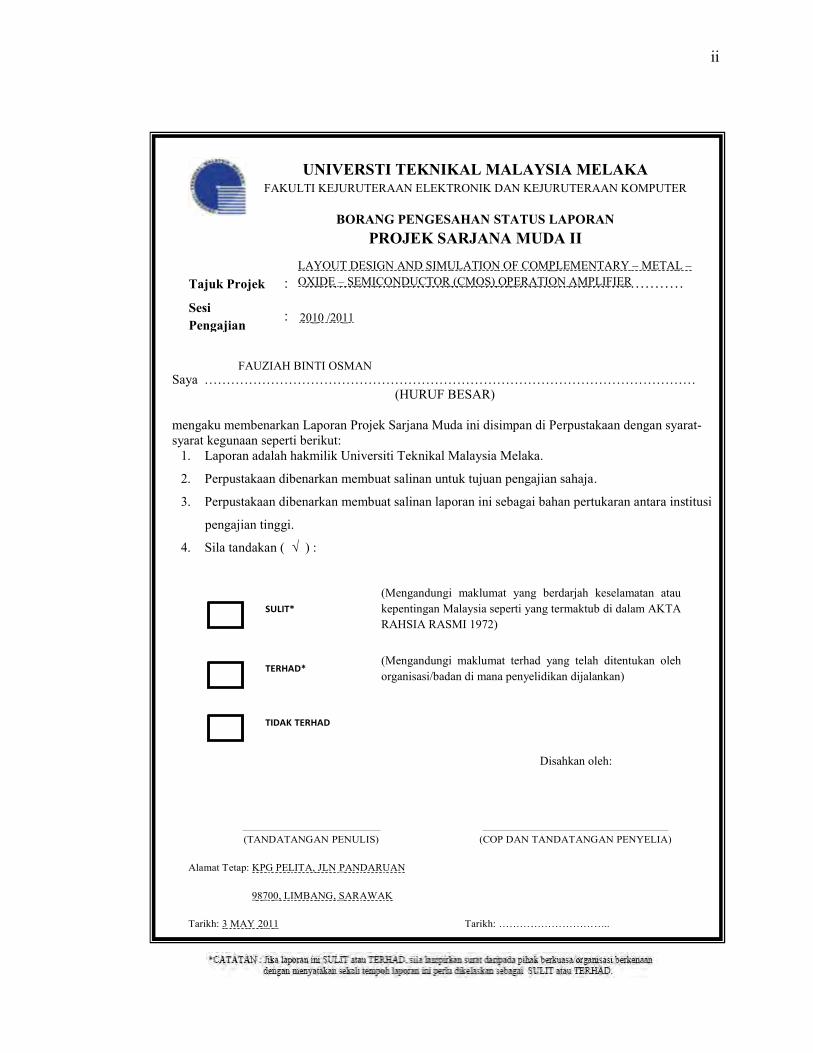
UNIVERSTI TEKNIKAL MALAYSIA MELAKA FAKULTI KEJURUTERAAN ELEKTRONIK DAN KEJURUTERAAN KOMPUTER
BORANG PENGESAHAN STATUS LAPORAN
PROJEK SARJANA MUDA II LAYOUT DESIGN AND SIMULATION OF COMPLEMENTARY – METAL – OXIDE – SEMICONDUCTOR (CMOS) OPERATION AMPLIFIER
2010 /2011
FAUZIAH BINTI OSMAN Saya …………………………………………………………………………………………………
(HURUF BESAR) mengaku membenarkan Laporan Projek Sarjana Muda ini disimpan di Perpustakaan dengan syarat- syarat kegunaan seperti berikut:
1. Laporan adalah hakmilik Universiti Teknikal Malaysia Melaka.
2. Perpustakaan dibenarkan membuat salinan untuk tujuan pengajian sahaja.
3. Perpustakaan dibenarkan membuat salinan laporan ini sebagai bahan pertukaran antara institusi
pengajian tinggi.
4. Sila tandakan ( √ ) :
(Mengandungi maklumat yang berdarjah keselamatan atau kepentingan Malaysia seperti yang termaktub di dalam AKTA RAHSIA RASMI 1972)
(Mengandungi maklumat terhad yang telah ditentukan oleh organisasi/badan di mana penyelidikan dijalankan)
Disahkan oleh:
(TANDATANGAN PENULIS) (COP DAN TANDATANGAN PENYELIA)
Alamat Tetap: KPG PELITA, JLN PANDARUAN
98700, LIMBANG, SARAWAK
Tarikh: 3 MAY 2011 Tarikh: …………………………..
SULIT*
TERHAD*
TIDAK TERHAD
: :
…………………………………………………………………… Tajuk Projek
Sesi Pengajian

iii
“I hereby declare that this report is the result of my own except for quotes as cited
clearly in the references.”
Signature : ...................................
Author : Fauziah binti Osman
Date : 3 May 2011
iv
“I hereby declare that I have read this thesis and in my opinion this report is
sufficient in terms of scope and quality for the award of the degree of
Bachelor of Electronic Engineering (Computer Engineering)”
Signature : ...................................
Supervisor : En. Zul Atfyi Fauzan bin Mohammed Napiah
Date : ..................................

v To my beloved parents, sisters, and friends, who have encouraged me throughout my
journey of education. A warm thanks to all.

vi
ACKNOWLEDGEMENT
Alhamdulillah, thank you to Allah S.W.T because of His blessing, I finally
complete and finish my final year project successfully.
During the process to complete my project objective, I do a lot of research,
either by using internet, reading past year thesis, reference books or journals. With
the guidance and support from peoples around me, I finally complete the project due
to the time given. Here, I want to give credit to those who helped me to achieve what
I had achieved in my final year project.
I would like to express my sincere gratitude and respect towards my project
supervisor, En. Zul Atfyi Fauzan bin Mohammed Napiah for his kind encouragement
and suggestions. Without his continued support and interest, the project would not be
like what it likes today. May Allah bless and reward them for their sincere endeavour
and contribution in the way of knowledge.
I also want to thanks to my beloved parents because without them, I will not
be able to do well in my final year project. They did give me a lot of support, both
from money and moral support to help me continue for what I had started on.
Thank you to all lecturers, staffs, friends and all who has directly and
indirectly involved on this project. Your helps and cooperation will never be
forgotten. May Allah bless and reward them for their sincere endeavour and
contribution in the way of knowledge.
vii
ABSTRACT
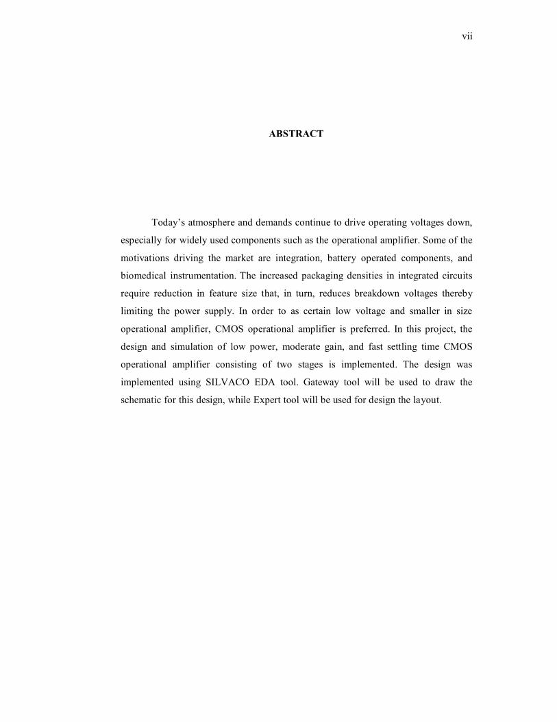
Today’s atmosphere and demands continue to drive operating voltages down,
especially for widely used components such as the operational amplifier. Some of the
motivations driving the market are integration, battery operated components, and
biomedical instrumentation. The increased packaging densities in integrated circuits
require reduction in feature size that, in turn, reduces breakdown voltages thereby
limiting the power supply. In order to as certain low voltage and smaller in size
operational amplifier, CMOS operational amplifier is preferred. In this project, the
design and simulation of low power, moderate gain, and fast settling time CMOS
operational amplifier consisting of two stages is implemented. The design was
implemented using SILVACO EDA tool. Gateway tool will be used to draw the
schematic for this design, while Expert tool will be used for design the layout.

viii
ABSTRAK
Dewasa ini permintaan dan keperluan bagi komponen-komponen elektronik
yang beroperasi dalam voltan rendah semakin meningkat terutamanya bagi
komponen yang banyak digunakan seperti penguat operasi. Beberapa motivasi yang
menggalakkan pasaran ialah integrasi, komponen yang menggunakan bateri dan
peralatan bio-perubatan. Peringkat kepadatan bungkusan bagi litar bersepadu
memerlukan komponen yang bersaiz tetapi dapat menghadkan sumber kuasa.
Alternatif yang paling berkesan dalam memenuhi keperluan ini adalah dengan
beralih kepada CMOS (Complementary Metal-Oxide-Semiconductor) yang
menawarkan komponen dengan keperluan kuasa yang rendah dan kecil dari segi saiz.
Dalam projek ini, rekabentuk dan simulasi penguat operasi CMOS yang mempunyai
ciri-ciri kuasa yang rendah dan gandaan yang sederhana serta terdiri daripada dua
peringkat telah diimplikasikan. Rekabentuk ini dilaksanakan menggunakan dalam
perisian SILVACO EDA. Pekakasan yang digunakan bagi lakaran skematik adalah
Gateway, manakala untuk melakar layout menggunakan perisian Expert.
ix
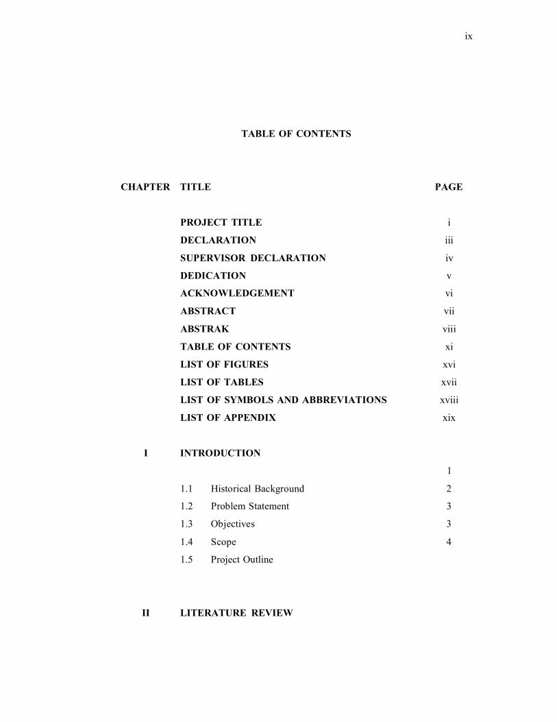
TABLE OF CONTENTS
CHAPTER TITLE PAGE
PROJECT TITLE i
DECLARATION iii
SUPERVISOR DECLARATION iv
DEDICATION v
ACKNOWLEDGEMENT vi
ABSTRACT vii
ABSTRAK viii
TABLE OF CONTENTS xi
LIST OF FIGURES xvi
LIST OF TABLES xvii
LIST OF SYMBOLS AND ABBREVIATIONS xviii
LIST OF APPENDIX xix
I INTRODUCTION
1
1.1 Historical Background 2
1.2 Problem Statement 3
1.3 Objectives 3
1.4 Scope 4
1.5 Project Outline
II LITERATURE REVIEW

x
TABLE OF CONTENTS
CHAPTER TITLE PAGE
2.1 MOSFET (Metal-Oxide-Semiconductor Field 5
Effect Transistor)
2.2 Modes of operation 7
2.2.1 Cut-Off or Sub-Threshold Mode 7
2.2.2 Triode or Linear Region 7
2.2.3 Saturation 8
2.2.4 CMOS (Complementary-Metal-Oxide 9
Semiconductor)
2.3 CMOS Operational Amplifier 10
2.4 Ideal Op Amp 11
2.5 Modes and Parameters 12
2.5.1 Open - Loop Gain 12
2.5.2 Input Common Mode Range 13
2.5.3 Output Voltage Swing 13
2.5.4 Unity Gain Frequency 14
2.5.5 Slew Rate 15
2.6 Two-Stage Operational Amplifier Design 15
2.6.1 Current Mirror 17
2.6.2 Differential Amplifier 18
2.6.3 Two Stage Operational Amplifier 18
Architecture Relationships
2.7 Compensation 20
2.8 Layout Design Rules 22
2.9 Transistor Layout 23

xi
TABLE OF CONTENTS
CHAPTER TITLE PAGE
2.9.1 Relief the Stress 24
2.9.2 Protect the Gate 25
2.9.3 Improve Yield 27
2.9.4 Bulk Connection 27
III METHODOLOGY
3.1 Methodology 28
3.2 Methodology Flowchart 30
3.3 Schematic Process Flow 32
3.4 Layout Process Flow 33
3.5 Design Schematic 35
3.6 Design Objective 36
3.7 Design 37
3.7.1 DC Gain 37
3.7.2 Common-Mode Input Range 38
3.7.3 Output Swing 38
3.7.4 Power Dissipation 39
3.7.5 Unity Gain Frequency 39
3.8 Design Steps 39
3.9 Circuit Design 44

xii
TABLE OF CONTENTS
TITLE PAGE
RESULTS AND DISCUSSIONS
4.1 The layout of CMOS operational amplifier 46
4.1.1 The Basic CMOS
Layout
4.1.2 The
Amplifier Layout
4.2 Design Rules Check (DRC)
4.3 Layout versus Schematic (LVS)
4.4 Discussions
CONCLUSION AND SUGGESTION
6.1 Conclusion 63
6.2 Suggestions
6.3 Commercialization Potential
REFERENCE
APPENDIX A
CHAPTER
IV
V
Operation
CMOS
Amplifier 47 Operation 54
59
60
61
Compact of
64
64
65 67

xiii
TABLE OF CONTENTS CHAPTER TITLE PAGE
APPENDIX B
APPENDIX C
APPENDIX D
APPENDIX E
APPENDIX F
68
70
72
74
76
LIST OF FIGURES
TITLE
MOSFET Structure
Comparison of Enhancement-Mode and Depletion-Mode
MOSFET Symbol
Cross Section of MOSFET Operating in Linear Region
Cross Section of MOSFET is Saturation Region
CMOS Symbol for NMOS and PMOS
Block Diagram of a General Two-Stage CMOS Op-Amp
Symbol of an Op-Amp
Configuration for the Measurement of the Open Loop-
Gain
The Configuration for Measurement of CMR
The Configuration for Measurement of Output Voltage
Swing
Unity Gain Frequency
Slew Rate
Two Stage Operational Amplifier
Current Mirror
Differential Amplifier
Single-Loop Negative Feedback System
Compensation Capacitor
Folded to Compact Transistor
Bird-Peak
xiv
PAGE
5
6
7
8
9
10
11
13
13
14
14
15
16
17
18
20
21
23
24
NO. 2.1
2.2 2.3
2.4
2.5
2.6
2.7
2.8 2.9
2.10 2.11
2.12
2.13
2.14
2.15
2.16
2.17
2.18
2.19
LIST OF FIGURES
NO. TITLE
2.20 Mechanical Stress from STI on Diffusion
2.21 Dummy Transistor
2.22 Measures to Protect the Gate
3.1 Project Flowchart
3.2 Process Flow of the Schematic Phase
3.3 Process Flow for Layout Process
3.4 The Schematic Design for the CMOS Operational
Amplifier
3.5 The Complete Schematic Design for the CMOS
Operational Amplifier.
4.1 Schematic Design of CMOS Operation Amplifier
4.2 Pdiff Cells for (a) M8 and (b) M5
4.3 Pdiff Cells for (a) M1 and (b) M2
4.4 Pdiff Cell for M7
4.5 Ndiff Cell for M6
4..6 Ndiff Cells for (a) M3 and(b) M4
4.7 Complete Basic Layout of CMOS Operational Amplifier
4.8 M6 Four Fingers Transistor
4.9 M3 and M4 Three Fingers Transistor
4.10 M5 and M8 Three Fingers Transistor
4.11 M1 and M2 with Four Fingers Transistor
xv
PAGE
24
25
26
30
32
33
35
44
47
48
49
50
51
52
53
55
55
56
57

LIST OF FIGURES
NO. TITLE
4.12 M7 Four Finger Transistor
4.13 Complete Compact Layout of CMOS Operational
Amplifier
4.14 Simulation from DRC
4.15 Simulation from LVS
xvi PAGE
57
58
59
60

LIST OF TABLES
TITLE
Design Rules
Transistor values summary
xvii PAGE
22
44
NO. 1.0
2.0

xviii
LIST OF SYMBOLS, ABBREVIATIONS OR NOMENCLATURE
K - Transconductance parameter (in saturation)
Γ - Bulk threshold parameter
VT - Threshold voltage
λ - Channel length modulation parameter.
Gm - Tranconductance
Fu - Unity gain frequency
VDSAT - Saturation voltage
VGS - Gate to source voltage.
GBW - Gain bandwidth
W - Width
L - Length
DRC - Design rule check.
LVS l - Layout versus schematic.
S/D - Source/Drain

LIST OF APPENDICES
NO. TITLE
A Schematic Netlist of CMOS Operation Amplifier
B DRC Script For Folded and Multi-Finger Transistor
C LPE Summary File for Multi-Finger Transistors
D Hierarchical Spice File for Multi-Finger Transistors
E LPE Summary File for Folded Transistor
F Hierarchical Spice File for Folded Transistor
xix PAGE
67
68
70
72
74
76
CHAPTER I
INTRODUCTION
This project uses software SILVATO EDA tools for design and simulate for
layout. The background of the study is thoroughly elaborated. This chapter also outlined
on the objective and scope of the research.
1.1 Historical Background
The Metal–Oxide–Semiconductor Field-Effect Transistor (MOSFET) is a
voltage controlled device used to amplify electronic signals or acted as a switch. The
MOSFET includes a channel of n-type or p-type semiconductor material and is
accordingly called an NMOSFET or a PMOSFET (also commonly NMOS or PMOS). It
is one of the most common transistors used in both analog and mixed-signal circuits for
advanced integrated circuit (IC) design. MOSFET has the advantages which the
switching time is about 10 times faster than a bipolar transistor, very much smaller
switching current, and less affected by temperature when compared to bipolar transistor.

2
Complementary Metal-Oxide-Semiconductor (CMOS) technology is circuit
implementation using both PMOS and NMOS transistors on the same silicon chip.
CMOS designs typically offer high gain and speed at low power consumption. In
addition, CMOS scales well to smaller devices without drastic changes in performance.
The operational amplifier often referred to informally as an op amp, is a circuit
that provides extremely high-gain amplification of the difference in voltage between two
inputs. One input is known as the inverting input and the other is known as the non-
inverting input. There is only a single output. The input impedance of the inverting and
non-inverting inputs is extremely high. The output impedance of the op amp is very low.
The primary requirement of an op amp is to have an open loop gain that is
sufficiently large to implement the negative feedback concept. Most of the amplifiers do
not have a large enough gain. Consequently, CMOS op amps use two or more stages of
gain. One of the most popular op-amp is a two stage op amp. The first is because it is
simple yet robust implementation of an op amp and second it can be used as the starting
point for the development of other types of op amp.
1.2 Problem Statement
There are two problems. First, while the voltage gain is high, it is not predictable.
Second, in order for the circuit to function properly, the transistors used in differential
amplifiers must be matched exactly. The first problem can be corrected by using
negative feedback to control the gain. CMOS is use because they made from the same
block of silicon and it easier to match.

3
1.3 Objectives
The objectives of this project can be summarized as below: (i) To understand the use of SILVACO EDA tool. (ii) To design layout of Complementary Metal Oxide Semiconductor operational
amplifier. (iii) To validate the layout and schematic of the amplifier
1.4 Scope
This project is based on analog electronic devices and advanced integrated circuit
design fundamentals. It involves 2 basic concepts, design and verification using
SILVACO EDA tool software. (i) Gateway supports flat or hierarchical designs of any technology. Gateway readily
accepts legacy designs from other schematic editors (PSPICE, OrCAD,
Composer, etc) through EDIF 200 standard. Gateway can be used by large
design teams through global preferences and handles multiple designs and
technologies with specific workspaces [1].
(ii) Expert is a high performance hierarchical IC layout editor with full editing
features, large capacity and fast layout viewing. Expert provides high level of
design assistance with Netlist Driven Layout and parameterized cells (Pcells) [1].
4
1.5 Project Outline
This project is organized into five chapters as follows:
Chapter 1 clarifies the background of the study for this project. This chapter also
outlined on the objective and scope of the research.
Chapter 2 discusses the literature survey on the theories of an ideal operational
amplifier and its performance characteristics. This chapter also details the two stages
operational amplifier design technique consist of differential gain stage and common
source gain stage.
Chapter 3 presents the methodology for the two stages CMOS operational
amplifier design. The transistor sizes then calculated according to schematic.
Chapter 4 present results and discussion of CMOS operational amplifier
generated using SILVACO EDA tool. The discussion is about the finding and
observation from layout design performance.
Chapter 5 outlines the conclusion and suggestion for this work. Conclusion for
the overall project findings especially on the CMOS operational amplifier circuit is done
and the suggestion for the future works is also stated.

CHAPTER II
LITERATURE REVIEW
In this chapter, the basic theories of MOSFET transistors and the characteristics
of an ideal operational amplifier will be reviewed. The important relationships of two
stages CMOS operational amplifier is reviewed.
2.1 MOSFET (Metal – Oxide - Semiconductor Field Effect Transistor)
The metal – oxide - semiconductor field effect transistor (MOSFET, MOS-FET,
or MOS FET), is by far the most common field effect transistor in both digital and
analog circuits. Figure 2.1 shows the structure of MOSFET.
Figure 2.1: MOSFET Structure