~i.~,1,..:>.~.:,. ~~””,.*.&.‘:-.:,>ferretronix.com/tech/68k/an897.fsl.d.rev0.pdf ·...
TRANSCRIPT

@MO~OROLA AN897Semiconductor Products Inc. Appliution Note
,,
MC68008 MINIMUM CONFIGURATION SYSTL&&\*:~i.~.~.:,~~~.,,.:>>*!..},,,1,..~+r+,-\/\\~.,:~,,.(c,.,,.‘:-.:,>~~””,.*.&.Prepared by
.\:,:,.:~>”.~-~)~..,,e,....,.,~:,::~.!:*’,*,Geoffrey Brown and Kyle Harper ‘s.::<$,.$...
Advanced Microcomputer Applications Engineering.......... X..,..,:.,-t...~.~..y,...!,,:?,t,~~iij$,
Microprocessor Division ::&:,$j:$$?:$ ,Motorola Inc. $$t,,:$>,
.:>,:1..*\.*i$.Austin, Texas ~~..+~k~.:,,
,+j:~$~. ~~J\..**$.3.$,.x
.,~,,,.(,:.’:?.~~::~,$,,-’,:~,..~~,$~’,,.:..*,;<t~k ‘
,:$:{,’’~:~“‘**.,...$a\ii><....,\?>
,:i:<<.$\\.*.<,,..
INTRODUCTION,,.
(~S) by~~~r$essor and are terminated by the assertion of
This application note demonstrates the design of a simple data twer’acknowledge (DTACK) by the peripheral or
high-performance MC68~8 system that uses the MC68681 m~~o~’’:device being addressed. Figures 1-4 show the
Dual Universal Asynchronous Receiver Transmitter .~~n~um hardware necessary for an Mc68w8 system con-
(DUART) to interface with external devices. The MC68W8 is ~~vs;~ng ok
an exce~ent low-cost alternative to the MC68W and*),J~T*’*~ddress decode logic,
features an 8-bit data bus while maintaining software com-.~\,~\,>,..t!’.)“S$~~~YrDTACK generation logic,
patibility with the rest of the M68~ Family. TheMC68681 .$ “ Reset logic,DUART is an M68~ Family data communications X,@jp -that features:
Bus error generation logic,i*,\Ni’<. *1
TWO independent asynchronous sefial ch~nels ,$@~~&...,,.,
System memory,,,.+?.*$):~\*
A programmable l~bit counter/timer, Interrupt handting logic, and.<:$1,~. ,k.,,$;.,~**... ,.<.+~+I$++<,i:$A 6-bit pardel input port, and
An MC68681 interface... ‘{:>,..$,.‘+...-.!,.,,,<\“’’~...*<i.,~’s
An 8-bit pardel output port.:2$%,... \,,f$;i,..J.:$.~ The following paragraphs detail the required hardware as ap-
Emphasisin this design concept is pl~@~~~& performance,pfied to the design concept described in this application note.
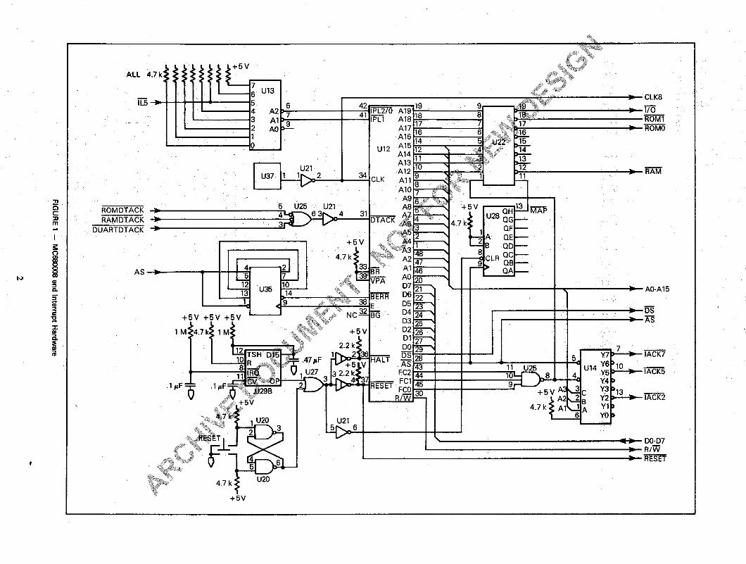
expandabihty, and low chip COU~$<,~?~):,,,3 Address Decode LogicThe M68~ system design p#@&~~ei’demonstrated in this The only tricky part of address decoding for an MC68W8
application note include: ,,,~t$:e>~kvs~ system is that the system ROM must be mapped to addressInterrupt hardware, ~ ‘?~~.* $m at reset. It would be impractical to fti the ROM at the
.i~>;~’.Peripheral interfac~@ ,, bottom of the address map, as this would not tiow for
Memory inter f~ce;~e&&ques,dynamic programming of interrupt vectors. To provide
Memory ref&@~,@itration in an M68~ system, anddynamic mapping of these interrupt vectors, an SN74LS164
Efficient,<~{#,&O software.shift register (U28) is used to generate a signal, MAP, whichis low for the first eight memory cycles after reset (the
The s~te~~’~escnbed in this design concept, features the number of cycles necessry to fetch the reset vector and stackfoHo,#Wwme: pointer). U28 is reset rdong with the processor and is clocked
,ig&~~* MC68W microprocessor, by the rising edge of ~. The ~ signrd generated by U28
+$~%ytes of ROM,is used by the address decoding circuitry to force selection of
&K bytes of dynamic RAM with no wait states, andROM when MAP is low and to dow normal memorydecoding when ~ is high.
An MC68681 DUART. In the design given in this application note, addressThe following paragraphs describe the hardware required decoding is accomplished by a PAL16L8 (U22). This PAL is
for a h~gh-perforrnance, expandable, low chip count programmed to generate eight chip-select signals from ten in-MC68M8 system fouowed by a description of the software put signals. The inputs to the PAL are the upper eight ad-necessary to initialize and drive the MC68681 DUART. dress tines (A12-A19), IACK (the NAND of the MC68W8
function code lines, FC&FC2), and the MAP signal. Four of
HARDWA~ REQU=MENTSthe PAL-generated chip-select fines are used in this design tolocate RAM at the address $m, ROM at $A~, and the
The MC68~8 has an asynchronous bus structure in which MC68681 at $F~. The four remaining chip-select tines arebus cycles are initiated by the assertion of address strobe avaflable for future system expansion.
I A:
ROMDTACK . 5 U25 U21GQw A
RAMDTACK
DUARTDTACK
‘s
m
+5V

w
mRIW
AS
mA@A15
A6 Mll I ion ) All
RFA5
M
4,2 U2
9+
RFA43131A
All Ill ~6
A2RFA3
RFA2 ,Ym; , , .,,.. .,, , , II 11 1{
,,, ,”
RFA1
RFAOU17
( I 14<. 2
MUX +SELECT~<
R FAO-RFA6
+-~~-[, ~-~ ~-, gu,l,,
‘~’t,:l,,.,,,,.s.j,.. ..... .. ..
.. ., ,, ,-

I
Vv
5
9~ “36
\8, fl %
Ts
K
+5V12
4.7 k10
12 DPRQ
,+ U31B *
I Qb“ *

-&-A2 7
13 Al “u-A~ ‘3
1 RS1
To12 U27 11 m
RESET 3 RESET
R/~ 8 R/w37 —
,, .-. .” - . .HxUA
3.6664 MHz 32 i - --lArKF4
Ul, U2, Ull, U17U3-U1OU12U13U14U15, U16U18U19U20
MCM666EMcW~lSN“
‘$: , -,.=:J:,
SN74S 153j-15
.-----LB-. .74LS146SN74LS136MCM68766MC66661CK17AI cQaQ
s> $ ~~>i,t~<., U21, UM~:t:>,i,.\>\v’ SN74LS04,,,..,~!,~+.,,,fA$,**’f.tw,
U22 PAL16L8A
~T:.J., U23 SN74LS05),*,“,., ... U24 SN74LS08
U25 SN74S1OU26, U27 SN74532U28 SN74LS164U29 MCN56U30, U31 .SN74F74U32, U36 DDu4-51mU33, U35 SN74LS175U37 K1114A, 8 MHz OSCu%U39
MC1466MC1489

DTACK Generation Logic
There are three possible sources of DTACK:
DUART DTACK,
RAM DTACK, and
ROM DTACK.
The DUART generates its own ~K, = for RAMis generated by the RAM control circuitry, and DTACK forROM is generated by an SN74LS175 quad flip-flop (U33).These three DTACK sources are NANDed together by U25and U21 to generate one processor DTACK.
Reset Logic
There are two sources of system reset:
Power-up reset, and
Pushbutton reset.
Power-up reset is generated by the timer (U29B) which pro-duces an active high pulse of approximately one-half secondduration. The pushbutton reset, which allows the user toreset the system without powering down, is generated by adebounced switch. These two reset signals drive RESET andHALT through SN74LS05 open-collector drivers (U23).
Bus Error Generation Logic
The bus error signal, BERR, is generated by anSN74LS175 quad fip-flop (U35). U35 counts clock pulsesthat occur after IS becomes asserted. If ~ is stilI assertedafter four rising edges of the E clock (between 5 and 6.5microseconds), U35 will generate BERR.
System Memory
asserted during both types of RAM cycles (normal andrefresh). CAS is generated only during normal cycles andmust be held asserted until the processor removes ~. Inorder to accomphsh this, the appropriate delay tap (80nanoseconds) is used to clock the SELECT signrd through aflip-flop (U31B). This fllp-flop is cleared when ~ isnegated. The output of this flip-flop is used for both theCAS signal and for the RAM DTACK. The 8 MHz MC68008allows the DTACK to be asserted up to 90 nanosecondsbefore data from memory is vafid on a read cyc~,,Thespecifications for MCM6665L15 dynamic ,,*”~
9*ies
guarantee that data is valid 75 nanoseconds af&g@$ .The memory refresh controller operates o~~~~~d~ciple of
cycle stealing. Refresh requests may o~,!.er betweenMPU bus cycles. If an MPU RAM c~@~~e&.&stoccurs dur-ing a refresh cycle, it will not be starte~~~~l the refresh cycleis finished. At periodic interv~~~ ~‘Free-running clock(U29A) clocks a fip-flop (U3$,A) ~#generate a refresh re-quest. This refresh reque$+~~+l~chronized with the MPUclock by two fip-flOpS ~w~~t
The MC68008 ac ,ati’i~l specifications guarantee onefalling clock edge d~*]~e~S high time and that there willbeat least a on~%~df~ck period of ~S high time followingthat clock ed@~$j*bitration between MPU and refresh re-quests ocw%:~~ing this one-half clock period. The refreshreques~ijskc~nizer consists of two SN74F74 flip-flops(U30)St~#e*~rst flip-flop (U30A) has as its input the refreshr~hest ~%gndfrom the refresh request flip-flop (U3 1A) and
~i,r~[%%fked by the MPU clock. The second flip-flop (U30B)~~h% as its input the output of the first synchronizer fip-flo~
The MC68008 system presented here has a system memory ‘*,~k{.#30A) and is clocked by the MPU clock qualified by ~
that consists of 16K bytes of ROM and 64K bytes of dynamic ‘~~$~~~~$high. This two-level synchronizer is used to ensure that therewill be no risk of the first synchronizer flip-flop (U30A)RAM (see Figure 2). Because system performance is critical ,,$ ‘:
in this design, a fairly complicated, but fast, dynamic * ‘control circuit has been designed (see Figure 3). This.wlr~tuses tw~elay lines to sequence RAS and to a~wy,theMUX, CAS, and DTACK sigmds. Delay lines @S,,Y~@ssaryin order to optimize memory cycle times and %~$~~$~ossibleto design the memory controller such th~$x~ystem canoperate without wait states.
...... .2,,.~i~,:l:, ..$,.,\\,A description of RAM refresh req~~~$hronization and
arbitration is given in the followin&)}~a@graphs. Note that,for now, a signal called SELE@~;~$3umed which initiatesrefresh cycles. The principl~,~#~i&rnents of this signal arethat it occurs periodically~d ‘&at it becomes asserted onlywhile ~ is negated. IR’add)~~n, the RAM decode signal isquafified with =S i~~&&#e$stocreate a RAM request signal.Either the SELE.&~$$kl or the RAM request signal mayinitiate a RA~,&~G~&R
The front<~n@\~~%heRAM controller consists of three ORgates (U* @o&ed by a three input NAND gate (U25)which in ~~~eeds into the first delay line (U32). Each of thethre~,~~ ~%+eshas as one of its inputs a signal from the sec-o~~ %~y:]ine (u36) which changes state in the midde of thern~ti cycle. The other inputs to these OR gates consist ofS~ECT, RAM request, and an inverted feedback pathfrom the output of the three input NAND. The initiation of aRAM cycle via either SELECT or RAM request causes theoutput of the NAND gate to go high. The output of theNAND gate is then held high by the inverted feedback pathuntil the feedback from the second delay line forces it low.The purpose of the feedback path from the second delay lineis to guarantee that the delay lines will be cleared and readyto begin another RAM cycle at the end of a cycle. The out-puts of the first delay line generate the RAS, MUX, and CASsignals. Both the RAS and address multiplex signals are
entering a metastable state due to a missed setup time, Theoutput of the synchronizer fllp-flop (U30B) is the SELECTsignal. Al three fllp-flops of the refresh circuitry are clearedafter the C=/RAMDTACK flip-flop (U31B) has beenclocked during the refresh cycle. Address multiplexing forthe RAM is done by four SN74S153 multiplexer (Ul, U2,U11, and U17) with the appropriate addresses routed to theRAMs by SELECT and MUX. Refresh addresses aregenerated by an SN74LS393 dual 4-bit counter (U19) whichis clocked by the refresh clock.
Interrupt Handting Logic
The interrupt handling logic must prioritize incominginterrupt requests and generate interrupt acknowledgesignals back to the interrupt sources. Interrupt prioritizationis accomplished with an SN74LS148 8-to-3 priority encoder(U13). The MC68008 supports three of the M68000 interruptlevels (interrupt levels two, five, and seven); therefore, onlytwo of the outputsofU13 are connected to the MC68008. AnSN74LS138 3-to-8 demultiplexer (U14) is used to generateIACK signals for interrupting devices. The SN74LS138 isenabled when ~S is asserted and FCO-FC2 are all high(indicating an interrupt acknowledge cycle). Because theMC68681 uses ody one of the interrupt levels (interrupt levelfive), the remaining two levels are available for future systemexpansion.
The MC68681 Interface
With these logic circuits in place, interfacing the MC68681to the MC68008 is trivial (see Figure 4). The RESET, R/~,and data bus tines (DO-D7) are connected directly betweenthe MC68681 and the MC68008. The 1/0 chip-select linegenerated by the address decode logic (1/0) is connected tothe MC68681 chip-select (C=) pin. These address lines are
6

used instead of AO-A3 in order to maintain hardware designconsistency with the other M68000 Family microprocessors(which do not have address fine AO). The MC68681 interrupt(IRQ) and interrupt acknowledge (IACK) pins are tied to the~ and IACK5 lines of the interrupt handhng logic, respec-tively, thus assigning the MC68681 interrupt a level 5 prior-ity. Finally, a 3.68@ MHz crystal is connected between theMC68681 X1/CLK and X2 pins. The crystal is required forthe on-chip baud-rate generator. 15 pF and 5 pF shuntcapacitors must dso be connected between the crystal andground as shown to ensure proper operation of the oscillator.
The MC68681 serial channels are connected to externaldevices via RS-232 drivers and DB-25 connectors. TheMC68681 OPO, IPO, OP1, and IP1 pins are used as the— — _RTSA, CTSA, RTSB, and CTSB handshake fines, respec-tively; therefore, they too are routed via the RS-232 driversto their. respective connectors.
THE DUART SO~WA~——
This design will use both of the channels and the RTS/CTShandshake capabilities of the DUART. The interface soft-ware required for this design is flowcharted in Figure 5 and islisted at the end of this document, There are three routines:
DINIT, INCH, and OUTCH.
DINIT is the DUART initialization routine and is executedupon system power-up. After DINIT initirdizes the DUARTchannels, it enables channel A and channel B in normaloperation mode. INCH is the input character routine. Uponentry, INCH requires the channel base address in addressregister AO. Upon return, the lower byte of data register DOwill contain the received character. OUTCH is the outputcharacter routine. Upon entry, OUTCH requires the channel
&&OUTCHR
FIGURE 5 – MC- Minimum System Sotiare Flowchans

MOTOROLA M68000 ASM vEQSION 1.30SYS : s. .41NSYSS
MINSYSS.S~ 07!20194 73:k4:qa PAGElof4
2
3OPT FRS)PCS,BRS
●
11121314
1s1617la19
202122
;:252b27
000FOOO1
000FOOO1000FOOOI000FOOO1000 FOO03000 FOO03
000 FOO05000FOO07000F0007
DUART EQU $OFOOO1
sCHANAMRIA
MR2ASRACSRACRARaATBA
EauEQUEQuEQUEQUEQUEQUEQU
DUARTtO3UAET+0
OUART+ODUART+20UART+2OUART+&DUART+6 ~OUART+~.\{;
A
28293031
;:343s36
000FOO09000FOO09000FOOOBOOOFOOOB000FOOO@000FOOOO
000FOOOF000FOOOF
IPC.RACRISRIMRcMsaCTURCLS9CTLR
INPUT PORT CHANGE REGISTERAUXILIARY CONTROL REGISTER
INTERRUPT ST4TUS REGISTERINTERRuPT MASK REGISTERCURRENT COUNTER/TIMER MOST SIGNIFICANT BYTECOUNTER/TIMER UPPER REGISTERCURRENT COUNTER/TIMER LEAST SIGNIFICANT aYTECOUNTER/TIMER LOWER REGISTER
3?383940414243444s46474a49
0UART+160UART+16DUAQT+16OUART+lBDUARTt13DUART+200UART+220UART+22
CHANNEL B BASE AODRESSMOOE REGISTER 19
MODE REGISTER 29
STATUS REGISTER aCLOCK-SELECT REGISTER 8coMhANo REGISTER aRECEIVER BuFFER a
TRANSMITTER aUFFER B
OOOFOQf:h:\+~;< “IVR EQu:!
DUART+24OOOF@~*&”r$ 1P
INTERRUPT VECTOR REGISTEREQU
S20UART+26
ooQFQ&,b~
INPUT PORT (UNLATCHED)OPCR EQU
S30UART+26
QQDFgoTbOUTPUT PORT CONFIGURATION REGISTER
$tibo,fholoSTRC EQU
S4DUART+2a START-COUNTER COMMAND
BTST EQU 0UART+2a,:<.>t>~@~~#OOIF STPC
OUTPUT PORT REGISTER aIT SET COMMANOEQU DUARTt30
;: *,,,,*g:}:@~’001 F,,?, BTRST EQUS7
0UART+30STOP-COUNTER COMMANDOUTPUT PORT REGISTER BIT RESET COMMANO
..,,.** CCNST4NTS

w
98
91
93


..

This information haa bean carefully chackad and Is believed to ba entirely relisble. However, no responsibility is assumed for inaccuracies. Motorola reservesthe right to make changes to any products herein to improve rallability, function ordeslgn. Motorola does not assume any liability arising out of the applicationor use of any product or circuit described herein. No license is conveyad under patent rights in any form. When this document contains information on a newproduct, specifications herein are subject to change without notice.
@MOTOROLA Semiconductor Products Inc.Colvilles Road, Kelvin Estate - East Kilbride/Glasgow - SCOTMND Printed in Switzerland