ie1204 digital design l8: memory elements: latches and
TRANSCRIPT

IE1204 Digital Design
L8: Memory Elements:
Latches and Flip-Flops.
Counter
Elena Dubrova
KTH / ICT / ES

• BV pp. 383-418, 469-471
This lecture
IE1204 Digital Design, HT14 2

Sequential System
A sequential system has a built-in memory - the output
depends therefore BOTH on the current and previous
value(s) of the input signal
a(t)
f(a(t))
Lecture 8 - Lecture 13
2IE1204 Digital Design, HT14

How do we get the hardware to
remember something?
• To remember something, we have to
somehow retain the information
• One way is to store information in the form of
a charge on a capacitance (DRAM)
• Another way is to let the information "run
around in a circle and bit its own tail"
4IE1204 Digital Design, HT14

• SR-latch can be implemented with NOR gates
• SET and RESET inputs are active high
• SET and RESET should not be active at the
same time!
SR-latch
(NOR)
IE1204 Digital Design, HT14 8
S R Qa Qb
0 0
0 1
1 0
1 1
0/1 1/0
0 1
1 0
0 0
(A) Circuit (B) Characteristic Table
Qa
Qb
R
S
(No change)
Prohibited input
combination (causes
oscillation)

SR-latch
(NAND)
IE1204 Digital Design, HT14
• SR-latch can also be implemented with
NAND gates
• SET and RESET inputs are active low
S
R
Qa
Qb
S R Qa Qb
0 0
0 1
1 0
1 1 0/1 1/0
1 0
0 1
1 1
(No change)
Prohibited input
combination

• To ensure that the state can only be changed
at certain points in time, a special Clock
signal is used
Construction of clocked latch
IE1204 Digital Design, HT14 9
Set /
Reset
Decoder
SR
Latch
SET
RESET
Q
Q
Latch
Inputs
CLK

Gated SR-Latch
S
Clk
R
"Prohibited location"
10IE1204 Digital Design, HT14
Clk S R Q(t+1)
0 x x Q(t) (no change)
1 0 0 Q(t) (no change)
1 0 1 0
1 1 0 1
1 1 1 x
Q
Q
R
S

Gated D-Latch
D
Clk
Q
Q
11IE1204 Digital Design, HT14
Clk D Q(t+1)
0 x Q(t)
1 0 0
1 1 1

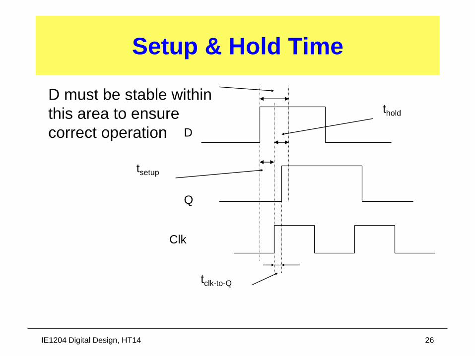
Setup & Hold Time
tsetup
tclk-to-Q
thold
D must be stable within
this area to ensure
correct operationD
Q
Clk
12IE1204 Digital Design, HT14

How do we create a sequence?
• We get a sequence if we take a value and then
determine the next value based on the current value.
Ex: 0,1,0,1, ...
the next value = NOT (present value)
• We need to process (invert) the current value and
then remember it until the next value is calculated
13IE1204 Digital Design, HT14

Sequential machines (cont.)
Clk
DQ
Q
D
Latch
NOT
Problems !!! If CLK is 1 for a long time, values with a
period of Tlatch+ TNOT just spin around
We want to design a storage element which changes its
state no more than once during one clock cycle
14IE1204 Digital Design, HT14

Master-slave D-flip flop
Solution: Connect the two D-
latches after each other!
D
Clk
D
Master
Q
Q
D
Slave
Q
Q
D
Negative edge
triggered D-flip flop
Invertion ring at CLK
indicates a negative edge.
15IE1204 Digital Design, HT14
Clk D Q(t+1)
0 0
1 1
1 x Q(x)
0 x Q(x)
x Q(x)

Timing Chart Master-slave
IE1204 Digital Design, HT14 16
D Q
Q
Master Slave
D
Clock
Q
Q
D Q
Q
Qm Qp
D
Clock
Qm
Q Qp=
Clk Clk

Positive edge-triggered D flip-flop
Q
Q
Clk = 0
D
17IE1204 Digital Design, HT14
D Q
QClock
If clock = 0, outputs of gates 2 and 3
are 1, so the output latch (gates 5
and 6) maintains its present state
1
2
3
4
5
6
1
1
D
D

Positive edge-triggered D flip-flop
IE1204 Digital Design, HT14
Q = D
Q = D
Clk = 1
DD Q
QClock
If clock = 1, the values on the outputs of
1 and 4 are transmitted through 2 and
3 to set inputs of 5 and 6 to D and D,
respectively. This sets, Q=D, Q=D
1
2
3
4
5
6
D
D
D
D
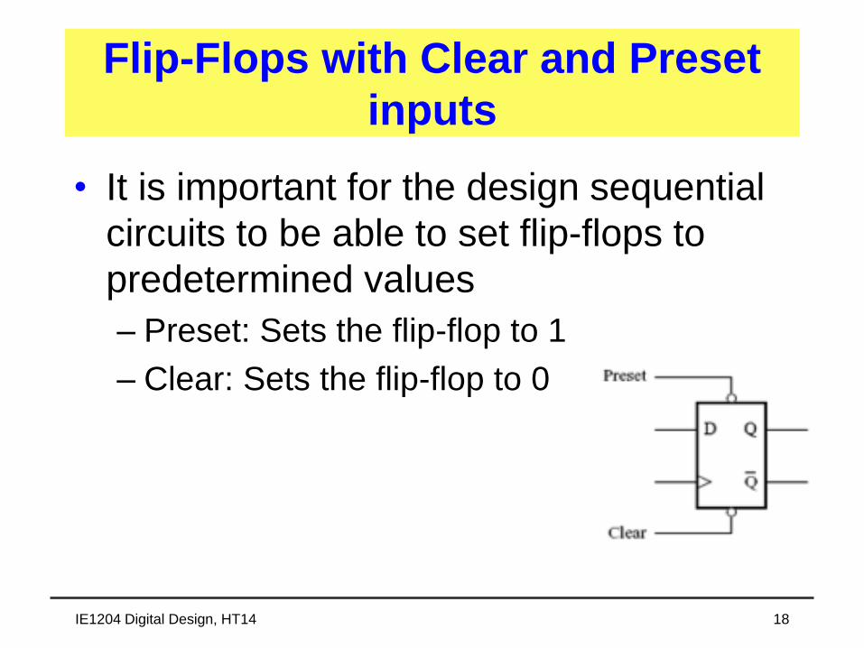
• It is important for the design sequential
circuits to be able to set flip-flops to
predetermined values
– Preset: Sets the flip-flop to 1
– Clear: Sets the flip-flop to 0
Flip-Flops with Clear and Preset
inputs
IE1204 Digital Design, HT14 18
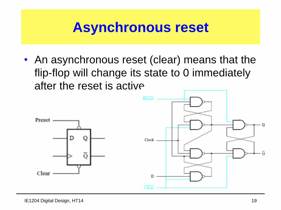
• An asynchronous reset (clear) means that the
flip-flop will change its state to 0 immediately
after the reset is active
Asynchronous reset
IE1204 Digital Design, HT14 19

• A synchronous reset causes the flip-flop
to take state 0 at the next clock edge
• Synchronous reset is implemented with
an additional logic
Synchronous reset
IE1204 Digital Design, HT14 20

Other common types of flip-flops
Q
Q
J
K
JK flip-flop (by Jack Kilby - Nobel Prize 2000)
Clk J K Q Q
0 0 Q(t) Q(t)
0 1 0 1
1 0 1 0
1 1 Q(t) Q(t)
Q
Q
T
T-flip-flop (T = Toggle)
Clk T Q Q
0 Q(t) Q(t)
1 Q(t) Q(t)
22IE1204 Digital Design, HT14
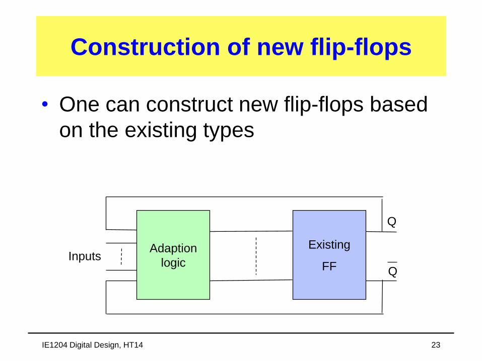
• One can construct new flip-flops based
on the existing types
Construction of new flip-flops
IE1204 Digital Design, HT14 23
Adaption
logic
Existing
FF
Q
Q
Inputs
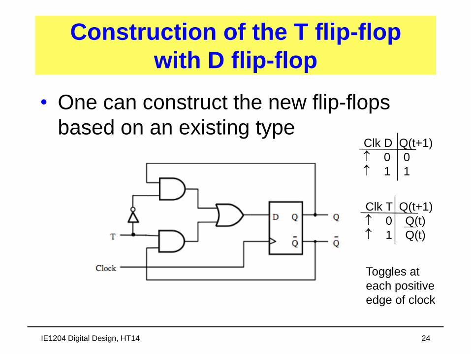
• One can construct the new flip-flops
based on an existing type
Construction of the T flip-flop
with D flip-flop
IE1204 Digital Design, HT14 24
Clk T Q(t+1)
0 Q(t)
1 Q(t)
Toggles at
each positive
edge of clock
Clk D Q(t+1)
0 0
1 1

• It is possible to determine the maximum
frequency in a sequential circuit by
having information about
– Gate delays tlogic
– Setup time tsu of flip-flops
– Hold time th of flip-flops
– Clock-to-output tcQ time
Timing Analysis
IE1204 Digital Design, HT14 25
Setup & Hold Time
tsetup
tclk-to-Q
thold
D must be stable within
this area to ensure
correct operation D
Q
Clk
26IE1204 Digital Design, HT14

What is the maximum frequency?
• Gate delays
– tlogic = tNOT = 1.1 ns
• Setup time
– tsu = 0.6 ns
• Hold time
– th= 0.4 ns
• Clock-to-output
– tcQ = 1.0 ns
IE1204 Digital Design, HT14 27
T = tsu + max(th,tcQ) + tlogic = 2.7 ns
F = 1/T = 370 MHz

• A shift register contains several flip-flops
• For each clock cycle, we shift all values from
left to right
• Many designs use shift registers and values
Q4, ..., Q1 as input to other components
Shift Register
IE1204 Digital Design, HT14 28

• One can realize a counter with flip-flops
• The examples below show an asynchronous
counter
• Some clock inputs are coupled to the Q
output of the previous flip-flop
Asynchronous counter
IE1204 Digital Design, HT14 29

Asynchronous 3-bit counter
IE1204 Digital Design, HT14 30
Clk T Q(t+1)
0 Q(t)
1 Q(t)
Toggles at
each positive
edge of clock

• In a synchronous counter clock inputs of
flip-flops are connected to the same
clock signal
Synchronous counter
IE1204 Digital Design, HT14 31

Synchronous counter
IE1204 Digital Design, HT14 32
Clk T Q(t+1)
0 Q(t)
1 Q(t)
Toggles at
each positive
edge of clock

• The critical path determines the maximum
frequency!
• This is the longest combinational path from Q0
through the two AND gates to the input of flip-
flop that computes Q3
– tlogic thus is equivalent to the delay of two AND gates
What is the maximum frequency?
IE1204 Digital Design, HT14 33

• Memory Elements
– Latches
– Flip-Flops
• Shift registers
• Counters
• Next lecture: BV pp. 485-507
Summary
IE1204 Digital Design, HT14 32