ieee catalog number cfp17gaa-art isbn: 978-1-5090-6070-2
TRANSCRIPT
Citation Wouter Steyaert, Patrick Reynaert (2017)
Layout Optimizations for THz Integrated Circuit Design in Bulk Nanometer CMOS
Proceedings of the CSICS 2017, 82–86.
Archived version Author manuscript: the content is identical to the content of the published
paper, but without the final typesetting by the publisher
Published version IEEE Catalog Number CFP17GAA-ART
ISBN: 978-1-5090-6070-2
Journal homepage https://csics.org/
Author contact [email protected]
+ 32 (0)16 325883
(article begins on next page)
brought to you by COREView metadata, citation and similar papers at core.ac.uk
provided by Lirias
Layout Optimizations for THz Integrated Circuit Designin Bulk Nanometer CMOS
Wouter Steyaert, Patrick Reynaert
ESAT-MICAS, KU Leuven, Leuven-3001, Belgium, [email protected]
Abstract—Scaling in CMOS has increased the attainable op-erational frequencies, while greatly increasing the transistor’sparasitic modeling complexity. Additionally, the performanceof the ever-smaller on-chip passives for mm-wave and THzcircuits is being degraded by numerous process requirementsand limitations, such as high densities of dummy metals. Thiswork discusses the main transistor layout trade-offs for high-frequency performance in both 40nm and 28nm bulk CMOS.The impact of dummy metals on a single-turn on-chip inductorfor mm-wave/THz frequencies is presented, which shows that lowdummy metal densities around critical high-frequency passivesare essential to minimize degradation in performance.
Index Terms—THz, CMOS, harmonics, transistor fmax,dummy fill
I. INTRODUCTION
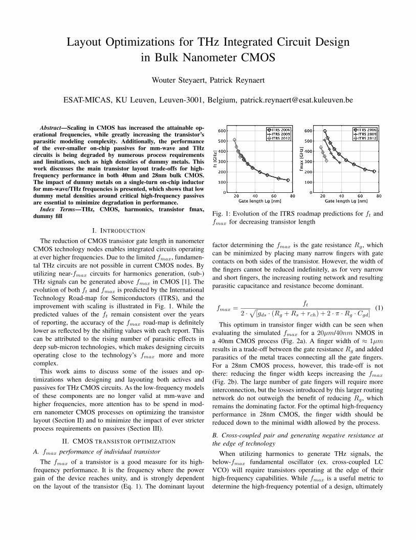
The reduction of CMOS transistor gate length in nanometerCMOS technology nodes enables integrated circuits operatingat ever higher frequencies. Due to the limited fmax, fundamen-tal THz circuits are not possible in current CMOS nodes. Byutilizing near-fmax circuits for harmonics generation, (sub-)THz signals can be generated above fmax in CMOS [1]. Theevolution of both ft and fmax is predicted by the InternationalTechnology Road-map for Semiconductors (ITRS), and theimprovement with scaling is illustrated in Fig. 1. While thepredicted values of the ft remain consistent over the yearsof reporting, the accuracy of the fmax road-map is definitelylower as reflected by the shifting values with each report. Thiscan be attributed to the rising number of parasitic effects indeep sub-micron technologies, which makes designing circuitsoperating close to the technology’s fmax more and morecomplex.
This work aims to discuss some of the issues and op-timizations when designing and layouting both actives andpassives for THz CMOS circuits. As the low-frequency modelsof these components are no longer valid at mm-wave andhigher frequencies, more attention has to be spend in mod-ern nanometer CMOS processes on optimizing the transistorlayout (Section II) and to minimize the impact of ever stricterprocess requirements on passives (Section III).
II. CMOS TRANSISTOR OPTIMIZATION
A. fmax performance of individual transistor
The fmax of a transistor is a good measure for its high-frequency performance. It is the frequency where the powergain of the device reaches unity, and is strongly dependenton the layout of the transistor (Eq. 1). The dominant layout
Fig. 1: Evolution of the ITRS roadmap predictions for ft andfmax for decreasing transistor length
factor determining the fmax is the gate resistance Rg , whichcan be minimized by placing many narrow fingers with gatecontacts on both sides of the transistor. However, the width ofthe fingers cannot be reduced indefinitely, as for very narrowand short fingers, the increasing routing network and resultingparasitic capacitance and resistance become dominant.
fmax =ft
2 ·√
[gds · (Rg +Rs + rch) + 2 · π ·Rg · Cgd](1)
This optimum in transistor finger width can be seen whenevaluating the simulated fmax for a 20µm/40nm NMOS ina 40nm CMOS process (Fig. 2a). A finger width of ≈ 1µmresults in a trade-off between the gate resistance Rg and addedparasitics of the metal traces connecting all the gate fingers.For a 28nm CMOS process, however, this trade-off is notthere: reducing the finger width keeps increasing the fmax
(Fig. 2b). The large number of gate fingers will require moreinterconnection, but the losses introduced by this larger routingnetwork do not outweigh the benefit of reducing Rg , whichremains the dominating factor. For the optimal high-frequencyperformance in 28nm CMOS, the finger width should bereduced down to the minimal width allowed by the process.
B. Cross-coupled pair and generating negative resistance atthe edge of technology
When utilizing harmonics to generate THz signals, thebelow-fmax fundamental oscillator (ex. cross-coupled LCVCO) will require transistors operating at the edge of theirhigh-frequency capabilities. While fmax is a useful metric todetermine the high-frequency potential of a design, ultimately

(a)
(b)
Fig. 2: Influence of W on fmax (simulated), comparisonbetween (a) 40nm and (b) 28nm CMOS
the purpose of the cross-coupled transistor pair is to generatea negative resistance to compensate for the losses of the LCresonator tank. Fig. 3 shows the real part of Ycross−coupled fordifferent cross-coupled ultra-low Vt (ULVT) transistor fingerwidths (F = 20µm) implemented in a 28nm CMOS process.The frequency where the negative resistance crosses fromnegative to positive is fgm, in analogy to the cross-coupledpair sometimes being referred to as ’negative gm’. Similar tothe impact on fmax, the optimal transistor finger width yieldsa larger negative resistance up to a higher fgm.
With parasitics becoming a non-negligible part of the tran-sistor, parasitic-aware design approaches can provide usefulfeatures. As illustrated in Fig. 3b, changing the supply voltagevaries the parasitic capacitance of the cross-coupled pair bya few femto-Farads. When the (fixed) capacitance of theVCO is kept small to enable a higher fundamental oscillationfrequency, the influence of this ’parasitic tuning’ would allowthe omission of additional varactors from the VCO whilemaintaining frequency tuning capabilities.
III. IMPACT OF DUMMY METALS ON PASSIVES INDEEP-SCALE NANOMETER CMOS
The scaling of CMOS technology nodes does not only meanthat the effective gate length decreases, but also has an impacton the metallization options available to the designer (Fig. 4).The amount of available metal layers has increased to cope
(a)
(b)
Fig. 3: Negative resistance (a) and parasitic capacitance (b)generated by a 28nm CMOS cross-coupled transistor pair
with the rising interconnection difficulties that come with theever-higher density of transistors.
Fig. 4: CMOS metal stack evolution towards deep-scalenanometer nodes
Another major evolution is in the thickness of the differentmetal layers, and the corresponding proximity to the siliconsubstrate. The lower layer metal thickness has reduced to verythin traces of ≈ 100nm−200nm thin, with a significant rise inthe trace sheet resistance. The resistance of vias between met-als, especially the lower metals, has also drastically increasedfor deep-scale nanometer CMOS technologies [2]. While themiddle and top metal layer thickness has not changed thatimmensely over newer technology nodes, the reduction of the

lower metals results in a closer proximity of the higher metalsto the lossy substrate.
The importance of metal density rules in deep-scalenanometer CMOS technologies is becoming increasingly im-portant, both production process-wise as for the design ofhigh-frequency passives. When operating at the high-end ofthe mm-wave spectrum, passives become very small and thepresence of nearby dummy metals has an increasing impacton the passives performance. The impact of dummy metals ontransformers and inductors up to 60GHz has already shownthat for mm-wave frequencies, there is a noticeable influence[3]–[5]. In the following section, this work presents the impactof dummy metals on on-chip inductors used in THz circuits.
(a) (b)
Fig. 5: Close-up of dummy metals (a) and a single-turn on-chipinductor with surrounding dummy metals (b), both generatedby an automatic filling tool
(a) (b)
Fig. 6: Close-up of dummy metals (a) and a single-turn on-chip inductor with a 10% dummy metal density (b), manuallyplaced
The foundry-provided dummy filling tool aims to generate a80-90 percent metal density, and yields a dummy-filled layoutas depicted in Fig. 5. While this high, uniform metal density isgood to minimize any process-related variations, it is virtuallyimpossible to simulate due to the dense mesh of very narrowmetal strips. To analyze the impact of different dummy metaldensities at (sub-)mm-wave frequencies, a fixed dimensiondummy unit structure is manually placed to achieve 10 to 40percent metal density (as shown in Fig. 6) around an inductorwith 15µm inner diameter and 5µm trace width. Each unitdummy structure consists of metal square of all consecutivedummy metals. The structures are spaced evenly to achievethe desired density, and the inductor is implemented in thetop UTM layer and simulated in a 2.5D EM simulator (ADS
Momentum). Using 2.4µm x 2.4µm squares allows relativelyfast simulations while maintaining high simulation accuracy.
(a)
(b)
Fig. 7: Simulated inductor inductance (a) and quality factor(b) of a top-metal single-turn inductor with varying density ofmanually placed dummy metals
The resulting simulated inductance L and inductor qualityfactor Q for different dummy metal densities are shown in Fig.7. While the inductance does not vary greatly, an extensivedivergence is seen when looking at the quality factors of thevarious metal densities: the difference in quality factor withand without dummies increases at higher frequencies. At RFfrequencies, the impact of the dummy metals is minimal, whilea noticeable difference is detectable at mm-wave frequencies.The spread in quality factor between 0% and 40% dummy fillis 25% at 80GHz, while at 200GHz, adding 40% of dummiesdecreases the total quality factor by half compared to the same,dummy-free inductor.
The dominant loss mechanisms due to dummy filling arethe magnetically induced eddy currents in the dummy metalstructures and the additional capacitive coupling to the lossysilicon substrate. At low frequency (10GHz), the losses of theinductor are dominated by the resistive losses of the metalinductor trace and the eddy currents in the dummy metalsare minimal. At mm-wave frequencies (60GHz), the magneticfield of the inductor starts to induce observable eddy currentsin the top layers of the dummy structure. From this point on inthe frequency spectrum, the dummies start to have a substantialimpact on the quality factor of the inductor. At higher frequen-

cies (200GHz and 300GHz), the dummy structure becomes acapacitive path to the substrate, further increasing the totalparasitic capacitance to the substrate and lowering the self-resonance frequency of the inductor (993GHz/936GHz for0%/40% dummies). The losses are now both the eddy currentsbeing induced in all metal layers of the dummy structure, aswell as the increased coupling to the lossy silicon substrate.To verify that a major part of the losses is due to the presenceof metal dummies themselves and not because of couplingto the substrate, an inductor without substrate and 0%/30%dummies is simulated. The difference in inductance betweenthe two cases remains small, while the quality factor dropswith almost a third at 200GHz due to eddy currents.
Clearly, this shows that dummy metals have a significantimpact on the behavior of mm-wave and certainly THz pas-sives.
IV. IMPLEMENTATION OF THZ SIGNAL GENERATORS INBULK NANOMETER CMOS
Using the above-mentioned approaches, harmonic THz sig-nal sources are implemented in 40nm and 28nm bulk CMOS.The circuit topology is shown in Fig. 8a. The signal generationstarts with a LC-VCO with cross-coupled transistors to gen-erate the fundamental frequency. The VCO is connected to adifferential amplifier, which generates the third harmonic whilealso acting as a buffer between the output and the VCO core.This third harmonic is then coupled through a transformer tothe output load, being a probe pad or antenna.
(a)
(b) (c)
Fig. 8: Schematic and die photographs of a 0.54THz and0.6THz transmitter in resp. 40nm and 28nm bulk CMOS
A 0.54THz source [1] is implemented in 40nm CMOS (Fig.8b), with a 539-561GHz tuning range thanks to ’parasitictuning’: varying VDD1 changes the parasitic capacitance of thecore transistors. Frequency and output power measurementsfit well with simulations (Fig. 9). Additionally, a 588.9-613.6GHz transmitter with on-chip collinear dipole antenna [6]is fabricated in 28nm CMOS (Fig. 8c), demonstrating the first
THz signal generator in 28nm CMOS, despite the increasingparasitic complexity in advanced CMOS technologies [7].
(a) (b)
Fig. 9: Probe measurement results of a 40nm CMOS 0.54THzsignal source, showing frequency variation and power fluctu-ation with varying supply voltage VDD1 [1]
V. CONCLUSION
The design of THz circuits in CMOS is getting morecomplicated with scaling due to the increasingly dominantparasitics, the limitations in design freedom and influenceof metal density requirements on passives. In this work, acomparison between a 40nm and 28nm CMOS process ismade to determine the optimal finger width for highest fmax
and its ramifications for a cross-coupled VCO. Second, thiswork presents a study of the influence of dummy metals ona single-turn on-chip inductor designed for harmonics-basedTHz CMOS circuits. At mm-wave and THz frequency, thereis a significant degradation of the inductor quality factor dueto surrounding dummy metals. A minimum of dummy metaldensity should therefore be pursued and manually placed forthe critical mm-wave and THz components.
ACKNOWLEDGMENT
The authors would like to thank L. Tavernier and C. Annysfor their continuing support.
REFERENCES
[1] W. Steyaert and P. Reynaert, “A 0.54 thz signal generator in 40 nm bulkcmos with 22 ghz tuning range and integrated planar antenna,” Solid-StateCircuits, IEEE Journal of, vol. 49, no. 7, pp. 1617–1626, July 2014.
[2] J. Shi, K. Kang, Y. Z. Xiong, J. Brinkhoff, F. Lin, and X. J. Yuan,“Millimeter-wave passives in 45-nm digital cmos,” IEEE Electron DeviceLetters, vol. 31, no. 10, pp. 1080–1082, Oct 2010.
[3] D. Zhao and P. Reynaert, “A 60-ghz dual-mode class ab power amplifierin 40-nm cmos,” IEEE Journal of Solid-State Circuits, vol. 48, no. 10,pp. 2323–2337, Oct 2013.
[4] A. Tsuchiya and H. Onodera, “Patterned floating dummy fill for on-chipspiral inductor considering the effect of dummy fill,” IEEE Transactionson Microwave Theory and Techniques, vol. 56, no. 12, pp. 3217–3222,Dec 2008.
[5] L. Nan, K. Mouthaan, Y. Z. Xiong, J. Shi, S. C. Rustagi, and B. L.Ooi, “Experimental characterization of the effect of metal dummy fillson spiral inductors,” in 2007 IEEE Radio Frequency Integrated Circuits(RFIC) Symposium, June 2007, pp. 307–310.
[6] W. Steyaert and P. Reynaert, “A thz signal source with integrated antennafor non-destructive testing in 28nm bulk cmos,” in 2015 IEEE Asian Solid-State Circuits Conference (A-SSCC), Nov 2015, pp. 1–4.
[7] R. L. Schmid, A. C. Ulusoy, S. Zeinolabedinzadeh, and J. D. Cressler, “Acomparison of the degradation in rf performance due to device intercon-nects in advanced sige hbt and cmos technologies,” IEEE Transactionson Electron Devices, vol. 62, no. 6, pp. 1803–1810, June 2015.