ieee journal of selected topics in quantum …web.mit.edu/~hujuejun/www/my papers/journal...
TRANSCRIPT

IEEE JOURNAL OF SELECTED TOPICS IN QUANTUM ELECTRONICS, VOL. 24, NO. 2, MARCH/APRIL 2018 4000109
Hybrid Integration of III–V Solar Microcells forHigh-Efficiency Concentrated Photovoltaic Modules
Anna Tauke-Pedretti , Senior Member, IEEE, Jeffrey G. Cederberg, Jose L. Cruz-Campa, Member, IEEE,Charles Alford, Carlos A. Sanchez, Gregory N. Nielson, Murat Okandan, William Sweatt,
Bradley H. Jared, Michael Saavedra, William Miller, Gordon A. Keeler, Senior Member, IEEE,Scott Paap, John Mudrick, Anthony Lentine, Paul Resnick, Vipin Gupta, Jeffrey Nelson, Lan Li ,
Duanhui Li, Tian Gu, Member, IEEE, and Juejun Hu, Member, IEEE
(Invited Paper)
Abstract—The design, fabrication, and performance of InGaAsand InGaP/GaAs microcells are presented. These cells are inte-grated with a Si wafer providing a path for insertion in hybrid con-centrated photovoltaic modules. Comparisons are made betweenbonded cells and cells fabricated on their native wafer. The bondedcells showed no evidence of degradation in spite of the integrationprocess that involved significant processing including the removalof the III–V substrate.
Index Terms—Multijunction solar cells, wafer bonding, photo-voltaic cells, III–V solar cells, hybrid integration.
Manuscript received May 31, 2017; revised November 29, 2017 and Febru-ary 20, 2018; accepted February 26, 2018. Date of publication March 9, 2018;date of current version March 28, 2018. This work was supported in part bythe U.S. Department of Energy’s Laboratory Directed Research and Devel-opment (LDRD) program at Sandia National Laboratories and Advanced Re-search Projects Agency-Energy under the Micro-Scale Optimized Solar-CellArrays with Integrated Concentration (MOSAIC) program (DE-AR0000632).(Corresponding author: Anna Tauke-Pedretti.)
A. Tauke-Pedretti, C. Alford, C. A. Sanchez, W. Sweatt, B. H. Jared, M.Saavedra, W. Miller, G. A. Keeler, S. Paap, J. Mudrick, A. Lentine, P. Resnick,V. Gupta, and J. Nelson are with the Sandia National Laboratories, Albuquerque,NM 87185 USA (e-mail:,[email protected]; [email protected]; [email protected]; [email protected]; [email protected]; [email protected];[email protected]; [email protected]; [email protected]; [email protected]; [email protected]; [email protected]; [email protected];[email protected]).
J. G. Cederberg was with the Sandia National Laboratories, Albuquerque,NM 87185 USA. He is now with the MIT Lincoln Laboratory, Lexington, MA02421-6426 USA (e-mail:,[email protected]).
J. L. Cruz-Campa was with the Sandia National Laboratories, Albuquerque,NM 87185 USA. He is now with the Intel Corporation, Lehi, UT 84043 USA(e-mail:,[email protected]).
G. N. Nielson was with the Sandia National Laboratories, Albuquerque, NM87185 USA. He is now with the Vivint Solar, Lehi, UT 84043 USA (e-mail:,[email protected]).
M. Okandan was with the Sandia National Laboratories, Albuquerque, NM87185 USA. He is now with the mPower Technology, Albuquerque, NM 87110USA (e-mail:,[email protected]).
L. Li, D. Li, T. Gu, and J. Hu are with the Department of Material Sci-ence and Engineering, Massachusetts Institute of Technology, Cambridge, MA,02139 USA (e-mail:,[email protected]; [email protected]; [email protected]; [email protected]).
Color versions of one or more of the figures in this paper are available onlineat http://ieeexplore.ieee.org.
Digital Object Identifier 10.1109/JSTQE.2018.2812218
I. INTRODUCTION
THE marrying of disparate material systems through hybridintegration leads to more innovative devices. This is par-
ticularly true in optoelectronic devices where the electrical aswell as optical properties of the devices must be taken into con-sideration. There have been reports of combining Si and III-Vdevices for communications and here we discuss the hybrid in-tegration of Si and III-V photovoltaics for high efficiency solarmodules in a variety of environmental conditions.
The path to higher solar cell efficiencies has focused on col-lecting photons as close to their energy level as possible tominimize the solar energy lost to heat. This has been done withmulti-junction cell stacks of varying bandgaps spanning theentire solar spectrum. The typical method of integrating thesejunctions is monolithic epitaxial integration requiring currentmatching through all the junctions. These types of cells havedemonstrated the highest efficiencies to date [1]–[3]. However,as the number of junctions increase beyond three to four or moreepitaxial growth becomes more difficult due to lattice mismatchbetween materials. Also, current matching becomes more chal-lenging. Although there have been demonstrations of the growthof lattice mismatched materials on the same substrate to formmultijunction cells [1], [4], this approach requires tradeoffs inthe material quality and achievable bandgaps. Such limitationscan be overcome through direct wafer bonding or wafer bondingusing a dielectric bond layer.
Most of the demonstrations of hybrid integration of solarcells have focused on using the integration as a means toachieve higher efficiencies in traditional concentrated photo-voltaic (CPV) systems. However, these integration techniquescan also be used to enable new CPV systems applicable to awider variety of environments than traditional CPV. Sandia andothers have explored new PV modules and systems by scalingdown the size of the photovoltaic cells below 1 mm dimen-sions [4]–[9]. These smaller cells enable new optical designsbased on refractive optics and advanced module architectureswhich allow for a larger field of view, higher concentrations,reduced heating, and higher efficiencies. When coupled with adiffuse collection system, these architectures have the potential
1077-260X © 2018 IEEE. Personal use is permitted, but republication/redistribution requires IEEE permission.See http://www.ieee.org/publications standards/publications/rights/index.html for more information.
4000109 IEEE JOURNAL OF SELECTED TOPICS IN QUANTUM ELECTRONICS, VOL. 24, NO. 2, MARCH/APRIL 2018
to make concentrated photovoltaics viable in areas beyond thetypical high DNI (direct normal incidence) areas such as thesouthwest United States. In some cases, these systems could bereplacements for Si flat plate panels with much higher energyproduction. Two proposed examples of these systems includehybrid microscale photovoltaic systems as described in [5], [8]with separately connected junctions for maximum efficiency.Another concept is wafer integrated photovoltaics [9] whichutilizes a multi-functional Si platform which acts as a cell, opti-cal concentration element and integration platform for a moldedlens array [10], a multi-junction micro-cell array and the inter-connection layer. Calculations presented in [8] have shown thatcompared to conventional flat plate PV and CPV, there is the po-tential for an energy production boost of 40–50% and 15–40%across the U.S., respectively, with the collection of diffuse lightas well as direct light in a concentrated system.
High-performance, multi-junction microcells are key to thefeasibility of these module approaches. However, these systemspush unique requirements on the microcells. Intimate integrationis required between the III-V cells and Si cells including low-loss optical transparent transitions between cells and electricalconnections to a common interconnection plane. Cost models[11] for such systems require the judicious use of the expensivecompound semiconductor material meaning only the epitaxiallayers are used in the module while the substrate should beavailable for reuse. The optical designs push to smaller andsmaller cell sizes. Wafer level bonding of cells or solder bumpbonding of III-V cells to Si provides a path to achieving theserequirements.
In this paper we discuss important aspects of microcell de-sign in Section II. In Sections III and IV demonstrations ofGaAs/InGaP dual junction cells and InGaAs single-junctioncells respectively are presented. Data from cells fabricated ontheir native growth wafer are compared to cells bonded to Si inboth instances.
II. MICROCELL DESIGN
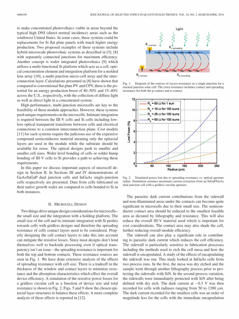
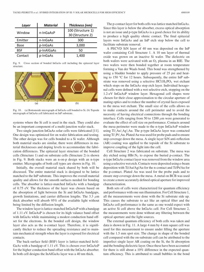
Two things drive unique design considerations for microcells–the small size and the integration with a holding platform. Thesmall size of the cell and its intimate integration with Si pushestowards cells with gridless designs and therefore the spreadingresistance of cells contact layers need to be considered. Prop-erly designing the cell contact layers to take this into accountcan mitigate the resistive losses. Since most designs don’t lendthemselves well to backside processing even if optical trans-parency isn’t an issue – the spreading resistance is important forboth the top and bottom contacts. These resistance sources areseen in Fig. 1. We have done extensive analysis of the effectsof spreading resistance with cell size. There is a tradeoff in thethickness of the window and contact layers to minimize resis-tance and the absorption characteristics which effect the overalldevice efficiency. A simulation of the resistive power losses fora gridless circular cell as a function of device size and totalresistance is shown in Fig. 2. Figs. 5 and 9 show the chosen epi-taxial layer structures to balance these effects. A more completeanalysis of these effects is reported in [12].
Fig. 1. Diagram of the sources of excess resistance in a single junction for astacked junction solar cell. The extra resistance includes contact and spreadingresistance for both the p-contact and n-contact.
Fig. 2. Simulated power lost due to spreading resistance vs. optical apertureradius. Simulation assumes maximum current extraction from an InGaP/GaAsdual junction cell with a gridless circular aperture.
The parasitic dark current contributions from the sidewalland non-illuminated areas under the contacts can become quitesignificant in microcells due to their small size. The semicon-ductor contact area should be reduced to the smallest feasiblearea as dictated by lithography and resistance. This will alsoreduce the overall III-V material used which is important forcost considerations. The contact area may also shade the cell,further reducing overall module efficiency.
The sidewall can also play a significant role in contribut-ing to parasitic dark current which reduces the cell efficiency.The sidewall is particularly sensitive to fabrication processesincluding the methods used to etch the cell mesa and how thesidewall is encapsulated. A study of the effects of encapsulatingthe sidewall was run. This study looked at InGaAs cells fromtwo process runs. In the first, the mesa was dry etched and thesample went through another lithography process prior to pro-tecting the sidewalls with SiN. In the second process variation,the sidewalls were immediately protected with SiN after beingdefined with dry etch. The dark current at −0.3 V was thenrecorded for cells with radiuses ranging from 50 to 1200 µm.The dark current recorded for the smallest cells was an order ofmagnitude less for the cells with the immediate encapsulation

TAUKE-PEDRETTI et al.: HYBRID INTEGRATION OF III–V SOLAR MICROCELLS FOR HIGH-EFFICIENCY 4000109
Fig. 3. Comparison of dark leakage current density for InGaAs cells fabri-cation with an immediate SiN passivation following the mesa etch (diamonds)and for a delayed passivation (squares). Leakage current is recorded at a biasvoltage of −0.3 V for both cell types.
Fig. 4. (a) Micrograph InGaP/GaAs cell bonded to Si substrate. (b) Micro-graph InGaP/GaAs cell for solder bump integration.
of the sidewalls. This shows the importance of sidewall passi-vation as the cells continue through the process. These resultsare shown in Fig. 3.
III. DUAL JUNCTION INGAP/GAAS CELLS
Sandia has designed and fabricated InGaP/GaAs dual junc-tion cells for integration via solder bump bonding as well aswafer bonding. Fig. 4(a) shows InGaP/GaAs cells wafer bondedto Si and Fig. 4(b) shows an image of InGaP/GaAs cells for in-tegration with Si for integration using solder bump bonds. Thecell epitaxial design was an n-on-p design with an n-type emitterfor both cells and a tunnel junction between the two cells. Theepitaxial structure for the two cells is nominally the same, al-though as grown the structure was flipped for the bonded cell sothe cell would be right side up following bonding. The epitaxialstructure of the cell is shown in Fig. 5. This configuration pre-vents a direct comparison between bonded and unbonded cellswith the same epitaxy. However, since the cells share nominallythe same epitaxy they can be compared to look at the effects ofbonding on cell performance.
For the cell bonded to Si, the cell mesas were defined prior tobonding using a combination of wet and dry etches. The cellsare bonded to the Si wafer with a SiN dielectric bond interfacewhich allows for electrical isolation between the InGaP/GaAscell and the Si. A 30 nm layer of PECVD SiN was depositedon the InGaP/GaAs cell wafer. While a 10 nm layer of thermaloxide was grown on the Si wafer. The dielectric on both wafers
Fig. 5. InGaP/GaAs cell epitaxial structure.
were activated with an O2 plasma in an RIE. The two waferswere then bonded together at room temperature forming a Vander Waals bond. This bond was strengthened by using a blad-der bonder to apply pressure of 25 psi and heating to 150 °Cfor 12 hours. The thickness of the dielectric bond interface wasdesigned to have reflective losses of <3% across the relevantsolar spectrum. The GaAs substrate was then removed by etch-ing an InAlP sacrificial layer to release the cells. The cell designemploys a topside n-GaAs contact layer which is designed toaccommodate the diffusion of AuGe/Ni/Au contacts and a bot-tom p-type contact layer of GaAs with a Ti/Pt/Au metallization.A citric acid wet etch is used to remove the GaAs contact layerand expose the AlInP window layer in the optical aperture duethe high selectivity between GaAs and AlInP. The cells fab-ricated on their native GaAs substrate used the same contactmetallization. The cell mesas were defined using a dry etch.
Following fabrication, the cells were tested in a solar simula-tor to access the cell performance. The one sun measurementswere done using an OAI class AAA solar simulator (from 300 to1800 nm) with an intensity of 1 sun and spectrum AM 1.5 cali-brated using a silicon reference solar cell. The output of the cellwas measured using an Agilent B1500a semiconductor deviceparameter analyzer. Cell efficiency, open circuit voltage (Voc)and short circuit current density (Jsc) were extracted from thecurrent-voltage curves obtained for each device. The currentdensity vs. voltage curves for bonded and on-substrate cells areshown in Fig. 6. The bonded cell has a circular aperture witha radius of 125 µm for an optical aperture area of 0.049 mm2,the on-substrate cell has a 1 mm2 optical aperture. The bondedcell efficiency, fill factor, open circuit voltage, Voc, and shortcircuit current density, Jsc, were measured to be 24.4%, 82.4%,2.13 V and 13.9 mA/cm2 respectively. The on-wafer cell effi-ciency, fill factor, open circuit voltage, Voc, and short circuitcurrent density, Jsc, were measured to be 25.4%, 82.3%, 2.22 Vand 13.8 mA/cm2 respectively. The curves are very similar inshape with nearly identical fill factors and short circuit cur-rent densities. The increase in Voc and thus efficiency for the

4000109 IEEE JOURNAL OF SELECTED TOPICS IN QUANTUM ELECTRONICS, VOL. 24, NO. 2, MARCH/APRIL 2018
Fig. 6. InGaP/GaAs micro-cell bonded on Si (red solid line) and on-wafer(blue dashed line) one sun J-V measurement curves.
Fig. 7. Normalized external quantum efficiency measurement forInGaP/GaAs cells bonded on Si.
on-wafer cell can be attributed to the larger cell size. As outlinedin Section II, the contribution for bulk dark current is signifi-cant for the 250 µm radius device as the junction area under thecontact metal outside the optical aperture accounts for 15.5%of the device junction area while this area accounts for 44.5%of the junction area for 1 mm square on-substrate device. Thisincreased bulk dark current contribution results in the lower Voc
seen for the smaller cell. This is all consistent with the InGaAsdata shown in Section IV.
The bonded cells were also tested under concentration andthe measurements are shown in Fig. 8. The scatter in the con-centration data at low concentrations is due to the single cellmeasured current being near the noise floor of the current me-ter. A fit is applied to the efficiency data and used to extracta maximum efficiency of 29.5% at 200 suns. As expected theopen circuit voltage increases with concentration. The decreasein fill factor observed with higher concentration is expected dueto spreading resistance in the optical aperture. We have previ-ously reported on the tradeoffs of cell size with resistance underconcentration and showed the advantages of micro-scale cellswith concentration without reducing the cell efficiency due toshading of electrical gridlines [13]. The external quantum effi-ciency of the cells was measured and is shown in Fig. 7. The
Fig. 8. InGaP/GaAs bonded cell performance measurements under concen-tration. The scatter in the data at low concentration is due to the current beingnear the noise limit of the current meter as is seen with the larger measurementerror bars. (a) # suns vs. efficiency. Line is a fit to the data. (b) # suns vs. Voc,(c) # of suns vs. fill factor.
efficiencies of these bonded cells match the design very closelyand there isn’t any obvious degradation from the bonding andsubstrate removal of the cells. This is also shown in the InGaAscells as is discussed in Section IV.
IV. INGAAS CELLS
InGaAs cells were designed for integration below an active Sicell to provide an added boost of efficiency at long wavelengthIR. These cells would be especially relevant in hybrid microscale
TAUKE-PEDRETTI et al.: HYBRID INTEGRATION OF III–V SOLAR MICROCELLS FOR HIGH-EFFICIENCY 4000109
Fig. 9. Cross section of bonded InGaAs cell including the epitaxial layerstructure.
Fig. 10. (a) Bottomside micrograph of InGaAs cell bonded to Si. (b) Topsidemicrograph of InGaAs cell fabricated on InP substrate.
systems where the Si cell is used in the stack. They could alsobe an important component of a multi-junction wafer stack.
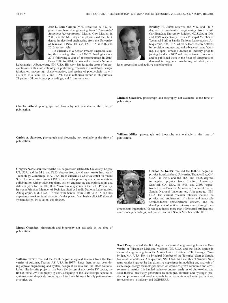
Two single junction InGaAs solar cells were fabricated [11].One design was optimized for on wafer fabrication and testing.The other design was for cells bonded to a Si wafer. Althoughboth material stacks are similar, there were differences in ma-terial thicknesses and doping levels to accommodate the fabri-cation differences. The epitaxial layer structure of the bondedcells (Structure 1) and on substrate cells (Structure 2) is shownin Fig. 9. Both stacks were an n-on-p design with an n-typeemitter. Micrographs of both cell types are shown in Fig. 10.
Initially, the overall material stack shared by both will bediscussed. The entire material stack is designed to be latticematched to the InP substrate. This improves the overall materialquality and allows for the smooth surfaces needed for bondingcells. The absorber is lattice-matched InGaAs with a bandgapof 0.75 eV. The thickness of the layer was chosen based onthe absorption of light between the Si and InGaAs bandgaps,growth limitations, and carrier diffusion lengths. The 3.3 µmthick absorber will absorb 95% of the available light withoutbeing limited by the diffusion length.
The window layer is lattice-matched InGaAsP with a bandgapof 1.11 eV. InGaAsP is chosen for its high valance band offsetwith InGaAs while maintaining a modest conduction band off-set for the electrons. In the bonded cell design, the windowlayer also acts as the n-contact layer. Therefore, it is signifi-cantly thicker to reduce the spreading resistance and to main-tain mechanical strength when the layer is exposed for electricalcontacts.
The back-surface field (BSF) layer is lattice-matched InAl-GaAs with a bandgap of 1.11 eV. This is chosen over InGaAsPfor the higher conduction band offset with the InGaAs absorber.In both cell designs the InAlGaAs layer was a 40 nm thick.
The p-contact layer for both cells was lattice matched InGaAs.Since this layer is below the absorber, excess optical absorptionis not an issue and p-type InGaAs is a good choice for its abilityto produce a high quality ohmic contact. The final epitaxiallayers were InGaAs and an InP etch stop below the cell tofacilitate substrate removal.
A PECVD SiN layer of 40 nm was deposited on the InPwafer containing Cell Structure 1. A 10 nm layer of thermaloxide was grown on an inactive Si wafer. The dielectric onboth wafers were activated with an O2 plasma in an RIE. Thetwo wafers were then bonded together at room temperatureforming a Van der Waals bond. This bond was strengthened byusing a bladder bonder to apply pressure of 25 psi and heat-ing to 150 °C for 12 hours. Subsequently, the entire InP sub-strate was removed using a selective HCl:H3PO4 wet etchantwhich stops on the InGaAs stop etch layer. Individual hexago-nal cells were defined with a wet selective etch, stopping on the1.2-eV InGaAsP window layer. Hexagonal cell shapes werechosen for their close approximation to the circular aperture ofmating optics and to reduce the number of crystal faces exposedto the mesa wet etchant. The small size of the cells allows usto make contacts around the cell perimeter and to avoid thenecessity of having electrical connections through the bondinginterface. Cells ranging from 50 to 1200 µm were generated toevaluate the effect of cell size on performance. Contacts aroundthe mesa perimeter were made to the n-type InGaAsP windowusing Ti\Au\Ag\Au. The p-type InGaAs layer was contactedusing Ti\Pt\Au. Plated Au was used for probe pads and to ensurestep coverage down the mesa. A single layer SiN anti-reflection(AR) coating was applied to the topside of the Si substrate toimprove coupling of the light into the cell.
Cell Structure 2 was fabricated on substrate. The mesa wasdry etched using HBr:N2 to expose the buried p-contact. Then-type InGaAs contact layer was removed from the window areausing a selective wet etch. Contacts were deposited using e-beamdeposition with Ti/Au/Ag/Au for the n-contact and Ti/Pt/Au forthe p-contact. Plated Au was used for the probe pads and toensure step coverage down the mesa. A metal on BCB was usedto create a more accurately defined optical aperture for improvedcharacterization.
Both sets of cells were characterized for quantum efficiencyand performance with one sun illumination. For Cell Structure 1,all the measurements were done with the Si substrate side up.This causes the substrate to act like an optical filter and theInGaAs cell performance is the same as one would expect withan active Si cell above the InGaAs cell. For Cell Structure 2,the measurements were done without any filtering between theoptical aperture and the light sources.
The external quantum efficiency of both cells was taken anddata is shown in Fig. 11. A large 4 mm by 4 mm square cell wasused for this measurement to ensure under filling the aperturewith the 1.5 mm spot size. The change in shape of the bondedcell compared with the on-substrate cell can be attributed to theimperfect single layer AR coating on the Si, the Si absorptionand the bonding dielectric layer. Once these have been accountedfor there is still about a 10% difference in the expected quan-tum efficiency. This is attributed to small bubbles in the bond

4000109 IEEE JOURNAL OF SELECTED TOPICS IN QUANTUM ELECTRONICS, VOL. 24, NO. 2, MARCH/APRIL 2018
Fig. 11. External quantum efficiency measurements for InGaAs cells.
Fig. 12. Device active area vs. short circuit current density for bonded cellsand cells fabricated on substrate (1 sun with AM1.5 Global).
interface which has a broadband transmission of ∼70%. There-fore, the low hanging fruit to increase the device efficiencywould be to improve the bond interface and use a broadband,multi-layer top AR coating.
The one sun measurements were done using an OAI classAAA solar simulator (from 300 to 1800 nm) with an intensityof 1 sun and spectrum AM 1.5 calibrated using a silicon ref-erence solar cell. The output of the cell was measured usingan Agilent B1500a semiconductor device parameter analyzer.Cell efficiency, fill factor, open circuit voltage (Voc) and shortcircuit current density (Jsc) were extracted from the current-voltage curves obtained for each device. These parameters werethen plotted as a function of device area for both cell structures(Figs. 12–15).
Cell Structure 1 shows little variation in short circuit currentdensity with area as one would expect. However, Structure 2shows an increase in Jsc for smaller device areas. This is dueto the cells absorbing light from outside of the optical aperture,including light that is reflected off the substrate. The metalaperture mask was an attempt to alleviate this effect, but theresults indicate that the light scatter is beyond the mask extent.
Fig. 13. Device area vs. open circuit voltage for bonded cells and cells fabri-cated on substrate (1 sun with AM1.5 Global).
Fig. 14. Device area vs. efficiency for bonded cells and cells fabricated onsubstrate (1 sun with AM1.5 Global).
The much lower Jsc for Structure 1 is due to the portion of thespectrum absorbed by the Si substrate before the InGaAs cell.
Both cell structures demonstrate a reduction in Voc as thedevice area decreases. This can be attributed to two separate ef-fects: perimeter current and excess dark current from absorberunder the contacts. Cell Structure 2 has unilluminated absorberregions under the n-contact which contributes to the dark cur-rent. This area is proportionally larger as the cell size decreases.This is not applicable in Cell Structure 1 because there areno absorber areas shaded with contacts since the cell is back-contacted. The second cause for the decrease in Voc is perimeterdark currents which is applicable to both cells. The perimeterto area ratio increases as the cell size decreases leading to alarger relative contribution by these dark currents and causingthe decrease in Voc. Fill factors and efficiency follow the sametrends as Voc. The lower efficiency for Structure 1 is again dueto the optical filtering by the Si wafer.
A theoretical maximum efficiency of 6% was expected forthe Structure 1 cells. These cells demonstrated efficiencies of2.25–3% mostly limited by the low open circuit voltage and fillfactor. However, we know this comes from the material or cell

TAUKE-PEDRETTI et al.: HYBRID INTEGRATION OF III–V SOLAR MICROCELLS FOR HIGH-EFFICIENCY 4000109
Fig. 15. Device active area vs. fill factor for bonded cells and cells fabricatedon substrate (1 sun with AM1.5 Global).
design performance limitations since similar devices fabricatedon substrate exhibit similar Voc and fill factors.
Simulations were done to calculate the maximum short circuitcurrent from the cell taking into account reflection losses fromthe air-Si interface, absorption in the Si substrate and absorptionin the cell itself. The anti-reflection coating reduces the reflec-tion losses to 1.75% of the solar spectrum with energy below thebandgap of Si. There will also be some loss associated withthe bonded interface although that is not taken into account inthe simulations. From these calculations, the expected cur-rent from the cell with an ideal global AM1.5 spectrum is13.2 mA/cm2. However, our testing lamp deviates from ideal andadjusting the spectrum according to the manufactures data givesan expected current of 14 mA/cm2. This correlates well with the12.5–13.6 mA/cm2 measured in the actual devices indicatingthe bonded interface has maintained a low loss optical path.
V. CONCLUSION
Unique design considerations for microcells were introducedincluding how to design around the potentially increased spread-ing resistance from thin contact layers with perimeter con-tacts and parasitic dark current contributions from etched mesaperimeters. We have demonstrated III-V microcells intimatelyintegrated with Si which could be utilized in next generation con-centrated photovoltaic modules. Results from InGaP/GaAs andInGaAs hybrid cell configurations were reported. These cellsemployed integration techniques including wafer level bondingof processed cells and solder bonding of the cells. The cellsthemselves showed no evidence of degradation despite the inte-gration process, which involved significant processing includ-ing the removal of the III-V substrate. It is expected that suchintegration approaches could be extended to more advancedmulti-junction cells such as triple junction solar cells.
ACKNOWLEDGMENT
Sandia National Laboratories is a multimission laboratorymanaged and operated by National Technology and Engineering
Solutions of Sandia, LLC, a wholly owned subsidiary ofHoneywell International, Inc., for the under contract U.S.Department of Energy’s National Nuclear Security Administra-tion under contract DE-NA0003525.
REFERENCES
[1] M. A. Green et al., “Solar cell efficiency tables (version 49),” Prog. Pho-tovolt., Res. Appl., vol. 25, pp. 3–13, 2017, doi: 10.1002/pip.2855.
[2] K. Sasaki, T. Agui, K. Nakaido, N. Takahashi, R. Onitsuka, and T.Takamoto, “Development of InGaP/GaAs/InGaAs inverted triple junctionconcentrator solar cells,” in Proc. 9th Int. Conf. Concentrating Photovolt.Syst., Miyazaki, Japan, 2013, pp. 22–25.
[3] P. T. Chiu et al., “Direct semiconductor bonded 5J cell for space andterrestrial applications,” IEEE J. Photovolt., vol. 4, no. 1, pp. 493–497,Jan. 2014.
[4] X. Sheng et al., “Printing-based assembly of quadruple-junction four-terminal microscale solar cells and their use in high-efficiency modules,”Nature Mater., vol. 13, no. 6, pp. 593–598, 2014.
[5] G. N. Nielson et al., “Leveraging scale effects to create next-generationphotovoltaic systems through micro- and nanotechnologies,” Proc. SPIE,vol. 8373, pp. 837317-1–837317-10, 2012.
[6] G. N. Nielson et al., “Microscale PV cells for concentrated PV applica-tions,” in Proc. 24th Eur. Photovolt. Sol. Energy Conf., 2009, pp. 170–173.
[7] A. L. Lentine, G. N. Nielson, M. Okandan, W. C. Sweatt, J. L. Cruz-Campa, and V. P. Gupta, “Optimal cell connections for improved shading,reliability, and spectral performance of microsystem enabled photovoltaic(MEPV) modules,” in Proc. 35th IEEE Photovolt. Spec. Conf., 2010,pp. 003048–003054.
[8] M.W. Haney, T. Gu, and G. Agrawal, “Hybrid micro-scale CPV/PV archi-tecture,” in Proc. 40th IEEE Photovolt. Spec. Conf., 2014, pp. 2122–2126.
[9] T. Gu et al., “Wafer-level integrated micro-concentrating photovoltaics,”in Proc. Light, Energy, Environ., 2016, Paper PTh3A.1.
[10] B. Jared et al., “Micro-concentrators for a microsystems-enabled photo-voltaic system,” Opt. Express, vol. 22, no. 102, pp. A521–A527, 2014.
[11] S. Paap et al., “Cost analysis of flat-plate concentrators employing mi-croscale photovoltaic cells for high energy per unit area applications, inProc. 40th IEEE Photovolt. Spec. Conf., 2014, pp. 2926–2929.
[12] J. L. Cruz-Campa et al., “Power maximization in III-V sub-millimeter,radial front contacted cells for thin micro-concentrators,” presented at thePhotovoltaics Specialists Conf., Denver, CO, USA, June 2014, Paper 154.
[13] A. Tauke-Pedretti et al., “Bonded InGaAs cells for microsystems enabledphotovoltaic,” presented at the Photovoltaics Specialists Conf., Denver,CO, USA, Jun. 2014, Paper 172.
Anna Tauke-Pedretti (S’02–M’08–SM’15) re-ceived the B.S. degree in physics and the B.S.E. de-gree in electrical engineering from the University ofIowa, Iowa City, IA, USA, in 2001, and the M.S. andPh.D. degrees in electrical and computer engineeringfrom the University of California, Santa Barbara, CA,USA, in 2002 and 2007, respectively.
In 2008, she joined the Technical Staff at SandiaNational Laboratories, Albuquerque, NM, USA, andhas worked on a variety of compound semiconductoroptoelectronic devices. Her work has included opti-
cal injection locking, high-speed modulators, high-efficiency solar cells, andinfrared detectors. She has more than 60 conference and journal articles and hasbeen awarded 7 patents.
Jeffrey G. Cederberg received the B.S. degree in chemical engineering fromMontana State University, Bozeman, MT, USA, in 1994 and the Ph.D. degree inchemical engineering from the University of Wisconsin—Madison, Madison,WI, USA, in 2000. He was employed with Sandia National Laboratories,Albuquerque, NM, USA, from 2000 to 2015. While at Sandia, he was involvedwith many aspects of the materials science and device physics associated withthin film semiconductors. In 2015, he joined MIT Lincoln Laboratory as a StaffMember to continue work on compound semiconductor devices, focusing onsemiconductor lasers and their applications.
4000109 IEEE JOURNAL OF SELECTED TOPICS IN QUANTUM ELECTRONICS, VOL. 24, NO. 2, MARCH/APRIL 2018
Jose L. Cruz-Campa (M’07) received the B.S. de-gree in mechanical engineering from “UniversidadAutonoma Metropolitana,” Mexico City, Mexico, in2003, and the M.S. degree in physics and the Ph.D.degree in electrical engineering from the Universityof Texas at El Paso, El Paso, TX, USA, in 2007 and2010, respectively.
He currently is a Senior Process Engineer lead-ing the texturing efforts in 1366 Technologies since2016 following a year of entrepreneurship in 2015.From 2008 to 2014, he worked at Sandia National
Laboratories, Albuquerque, NM, USA. His work has fused the areas of micro-electronics with solar technologies performing research in simulation, design,fabrication, processing, characterization, and testing of photovoltaic materi-als such as silicon, III–V and II–VI. He is author/co-author in 26 journals,21 patents, 31 conference proceedings, and 31 presentations.
Charles Alford, photograph and biography not available at the time ofpublication.
Carlos A. Sanchez, photograph and biography not available at the time ofpublication.
Gregory N. Nielson received the B.S degree from Utah State University, Logan,UT, USA, and the M.S. and Ph.D. degrees from the Massachusetts Institute ofTechnology, Cambridge, MA, USA. He is currently a Chief Scientist for VivintSolar. He supervises product R&D for all solar power system components incollaboration with product suppliers, system engineering and optimization, anddata analytics for the 100,000+ Vivint Solar systems in the field. Previously,he was a Principal Member of Technical Staff at Sandia National Laboratories,Albuquerque, NM, USA. He was with Sandia from 2004 to 2015 and hasexperience working in all aspects of solar power from basic cell R&D throughsystem design, installation, and finance.
Murat Okandan, photograph and biography not available at the time ofpublication.
William Sweatt received the Ph.D. degree in optical sciences from the Uni-versity of Arizona, Tucson, AZ, USA, in 1977. Since then, he has been do-ing optical engineering and system design at Sandia and the other NationalLabs. His favorite projects have been the design of microsolar PV optics, thefirst extreme-UV lithography system, designing of the laser isotope separationsystems, several optical computing architectures, lithographically patterned mi-crooptics, etc.
Bradley H. Jared received the M.S. and Ph.D.degrees in mechanical engineering from NorthCarolina State University, Raleigh, NC, USA, in 1996and 1999, respectively. He is a Principal Member ofTechnical Staff at Sandia National Laboratories, Al-buquerque, NM, USA, where he leads research effortsin precision engineering and advanced manufactur-ing. He spent almost a decade in industry prior tojoining Sandia in 2007 and has performed, presentedand/or published work in the fields of ultraprecisiondiamond turning, micromachining, ultrafast pulsed
laser processing, and additive manufacturing.
Michael Saavedra, photograph and biography not available at the time ofpublication.
William Miller, photograph and biography not available at the time ofpublication.
Gordon A. Keeler received the H.B.Sc. degree inphysics from Lakehead University, Thunder Bay, ON,USA, in 1996, and the M.S. and Ph.D. degreesin applied physics from Stanford University,Stanford, CA, USA, in 1998, and 2003, respec-tively. He is a Principal Member of Technical Staff atSandia National Laboratories, Albuquerque, NM,USA. His current research interests include thephysics and engineering of micro- and nanoscalesemiconductor optoelectronic devices, and thedevelopment of optical microsystems through het-
erogeneous integration. He has coauthored more than 100 journal publications,conference proceedings, and patents, and is a Senior Member of the IEEE.
Scott Paap received the B.S. degree in chemical engineering from the Uni-versity of Wisconsin-Madison, Madison, WI, USA, and the Ph.D. degree inchemical engineering from the Massachusetts Institute of Technology, Cam-bridge, MA, USA. He is a Principal Member of the Technical Staff at SandiaNational Laboratories, Albuquerque, NM, USA. As a member of Sandia’s Sys-tems Analysis group, he has extensive experience in modeling and analysis ofearly-stage energy technologies based on cradle-to-grave economic and envi-ronmental metrics. He has led techno-economic analyses of photovoltaic andsolar thermal electricity generation technologies, biofuels and hydrogen pro-duction processes, and novel materials for air separation and water purificationfor customers in industry and DOE/EERE.

TAUKE-PEDRETTI et al.: HYBRID INTEGRATION OF III–V SOLAR MICROCELLS FOR HIGH-EFFICIENCY 4000109
John Mudrick, photograph and biography not available at the time ofpublication.
Anthony Lentine, photograph and biography not available at the time ofpublication.
Paul Resnick, photograph and biography not available at the time of publication.
Vipin Gupta, photograph and biography not available at the time of publication.
Jeffrey Nelson, photograph and biography not available at the time ofpublication.
Lan Li received the B.S. degree from the University of Science and Technol-ogy of China, Hefei, China, in 2010, and the Ph.D. degree from the Univer-sity of Delaware, Newark, DE, USA, in 2016, both in materials science andengineering. Currently, she works as a Postdoctoral Associate with the Mas-sachusetts Institute of Technology, Cambridge, MA, USA. Her research interestincludes microptic and nanophotonic device design and fabrication, infraredoptical glass materials, and integrated flexible photonics, etc.
Duanhui Li received the B.S. degree in materialscience and engineering from Tsinghua University,Beijing, China. He is currently working toward thePh.D. degree in the Department of Materials Scienceand Engineering, Massachusetts Institute of Technol-ogy, Cambridge, MA, USA. His research interestsinclude developing low-cost integrated microopticssystems for renewable energy.
Tian Gu received the B.S. degree in electrical en-gineering from the Beijing Institute of Technology,Beijing, China, and the Ph.D. degree in electricaland computer engineering from the University ofDelaware, Newark, DE, USA. He is currently a Re-search Scientist with Materials Processing Center andthe Department of Materials Science and Engineer-ing, Massachusetts Institute of Technology, Cam-bridge, MA, USA. His research interests includenano- and micro-photonics and integrated photonicsystems for energy conversion, chip-scale infrared
spectroscopy, flexible photonics, data communications, and metamaterials.
Juejun Hu received the B.S. degree from TsinghuaUniversity, China, in 2004, and the Ph.D. degree fromthe Massachusetts Institute of Technology (MIT),Cambridge, MA, USA, in 2009, and both in materialsscience and engineering. He is currently the MertonC. Flemings Career Development Associate Profes-sor at Department of Materials Science and Engi-neering, MIT. His primary research interests includeenhanced photon–matter interactions in nanopho-tonic structures. Prior to joining the MIT, he was anAssistant Professor with the University of Delawarefrom 2010 to 2014.