ieee journal of solid-state circuits, vol. 46, no. 6, june
TRANSCRIPT
IEEE JOURNAL OF SOLID-STATE CIRCUITS, VOL. 46, NO. 6, JUNE 2011 1337
7.4 Gb/s 6.8 mW Source Synchronous Receiverin 65 nm CMOS
Masum Hossain, Member, IEEE, and Anthony Chan Carusone, Senior Member, IEEE
Abstract—A high-frequency jitter tolerant receiver in 65 nmCMOS is presented. Jitter tolerance is improved by tracking cor-related jitter using a pulsed clock forwarded from the transmitterside. The clock receiver comprises two injection locked oscilla-tors to frequency-multiply, deskew, and adjust jitter trackingbandwidth. Different data rates and latency mismatch betweenthe clock and data paths are accommodated by a jitter trackingbandwidth that is controllable up to 300 MHz. Each receiver con-sumes 0.92 pJ/bit operating at 7.4 Gb/s and has a jitter toleranceof 1.5 UI at 200 MHz.
Index Terms—Injection locking, jitter tracking, source syn-chronous.
I. INTRODUCTION
P ARALLEL interfaces are becoming increasingly impor-tant to meet the aggregate bandwidth required between
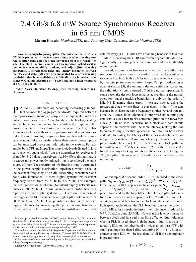
microprocessors, memory, peripheral components, networkhubs, storage devices, etc. A combination of technology scalingand architectural innovation has significantly improved thepower efficiency of these links over the years [Fig. 1(a)]. Thissummary includes both source synchronous and asynchronouslinks. For multilink high aggregate bandwidth interface sourcesynchronous links are useful where their power consumptioncan be amortized across multiple links in the system. For ex-ample, both QPI and HyperTransport include a dedicated link tocarry a synchronous clock from the transmitter to receiver andshared by 5–20 data transceivers. At 10+ Gb/s, timing marginis scarce and power supply induced jitter is considered the mainsource of jitter. The spectrum of this jitter is strongly correlatedto the power supply distribution impedance, which peaks atthe resonant frequency of on-die decoupling capacitance andbond wire inductance. In most digital systems this resonantfrequency varies from 50 MHz to 400 MHz. For example,the next generation Intel core (Nehalem) supply network res-onates at 300 MHz [1]. A similar impedance profile has beenreported in other digital systems [2]. Therefore, it is desiredthat high-speed I/O receivers have higher jitter tolerance from50 MHz to 400 MHz. One possible solution is to achievehigher tolerance by increasing the jitter tracking bandwidthof the receiver. Unfortunately most state-of-the-art clock and
Manuscript received September 10, 2010; revised January 12, 2011; acceptedMarch 09, 2011. Date of current versionMay 25, 2011. This paper was approvedby Associate Editor Jafar Savoj. This work was supported by Intel Corporationand Broadcom. Fabrication services were provided by CMC.The authors are with the Edward S. Rogers Sr. Department of Electrical and
Computer Engineering, University of Toronto, Toronto, ON, M5S 3G4 Canada(e-mail: [email protected]; [email protected]).Color versions of one or more of the figures in this paper are available online
at http://ieeexplore.ieee.org.Digital Object Identifier 10.1109/JSSC.2011.2131730
data recovery (CDR) units have a tracking bandwidth less than10 MHz. Increasing the CDR bandwidth beyond 100 MHz cansignificantly increase power consumption and stress stabilityrequirements.Instead, a source synchronous receiver can track jitter on a
source-synchronous clock forwarded from the transmitter asshown in Fig. 1(b). In these links static phase offset is correctedby per pin phase compensation loops. Per pin deskewing isdone at startup [3]; the optimum deskew setting is stored andthe calibration circuitry turned off during normal operation. Insome cases the deskew loop remains active during the normaloperation, but the tracking bandwidth is only on the order ofkHz [4]. Dynamic phase errors (jitter) are tracked using theforwarded clock whose jitter is correlated to that of the databecause both share the same frequency synthesizer and transmitcircuitry. Hence, jitter tolerance is improved by retiming thedata with a clock that tracks correlated jitter on the forwardedclock [5]. In an ideal scenario, both clock and data shouldappear at the receiver with the same latency, making the linktolerable to any jitter that appears in common on both clockand data. In reality, the latency of the clock and data paths arenot perfectly matched. Assuming a latency mismatch , thejitter transfer function (JTF) of the forwarded clock path canbe written as where is the jitter transferfunction of any clocking circuitry in the clock path. Using thisJTF, the jitter tolerance of a forwarded clock receiver can bewritten as
(1)
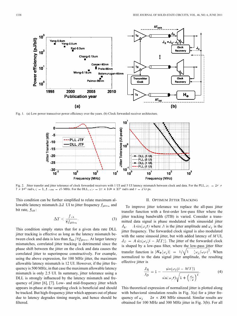
For example, if a second-order PLL is included in the clockpath, . Al-ternatively, if a DLL appears in the clock path,
where is thepole introduced by the loop filter. The JTF and jitter tolerancefor these two cases are compared in Fig. 2 with 5 UI and 1 UIof latency mismatch between the clock and data paths. In mosthigh speed applications, the PLL bandwidth is on the order of10–30 MHz. As a result, the link’s jitter tolerance is reduced to0.5 UI(peak) around 25 MHz. Note that the latency mismatchbetween clock and data paths has little effect on jitter tolerancewhen a PLL is used since high-frequency jitter is always fil-tered. A DLL on the other hand provides an all-pass JTF withsmall peaking (less than 1 dB). Assuming , jitter tol-erance using a DLL will be less than 0.5 UI if the denominatoris greater than 1:
(2)
0018-9200/$26.00 © 2011 IEEE
1338 IEEE JOURNAL OF SOLID-STATE CIRCUITS, VOL. 46, NO. 6, JUNE 2011
Fig. 1. (a) Low power transceiver power efficiency over the years. (b) Clock forwarded receiver architecture.
Fig. 2. Jitter transfer and jitter tolerance of clock forwarded receivers with 1 UI and 5 UI latency mismatch between clock and data. For the PLL,rad/s, , MHz. For the DLL, rad/s and ps.
This condition can be further simplified to relate maximum al-lowable latency mismatch UI to jitter frequency andbit rate, :
(3)
This condition simply states that for a given data rate DLLjitter tracking is effective as long as the latency mismatch be-tween clock and data is less than . At larger latencymismatches, correlated jitter tracking is detrimental since thephase shift between the jitter on the clock and data causes thecorrelated jitter to superimpose constructively. For example,using the above expression, for 100 MHz jitter, the maximumallowable latency mismatch is 12 UI. However, if the jitter fre-quency is 500MHz, in that case the maximum allowable latencymismatch is only 2.5 UI. In summary, jitter tolerance using aDLL is strongly influenced by the latency mismatch and fre-quency of jitter [6], [7]. Low- and mid-frequency jitter whichappears in-phase at the sampling clock is beneficial and shouldbe tracked. But high-frequency jitter which appears out of phasedue to latency degrades timing margin, and hence should befiltered.
II. OPTIMUM JITTER TRACKING
To improve jitter tolerance we replace the all-pass jittertransfer function with a first-order low-pass filter where thejitter tracking bandwidth (JTB) is varied. Consider a trans-mitted data signal is phase modulated with sinusoidal jitter
where is the jitter amplitude and is thejitter frequency. The forwarded clock signal is also modulatedwith the same sinusoid jitter, but with added latency of M UI,
. The jitter of the forwarded clockis shaped by a low-pass filter, where the low-pass jitter filter
transfer function is . Whennormalized to the data signal jitter amplitude, the resultingeffective jitter is
(4)
This theoretical expression of normalized jitter is plotted alongwith behavioral simulation results in Fig. 3(a) for a jitter fre-quency of MHz sinusoid. Similar results areobtained for 100 MHz and 300 MHz jitter in Fig. 3(b). For all

HOSSAIN AND CHAN CARUSONE: 7.4 Gb/s 6.8 mW SOURCE SYNCHRONOUS RECEIVER IN 65 nm CMOS 1339
Fig. 3. (a) Normalized jitter amplitude as a function of jitter tracking bandwidth. (b) Optimum jitter tracking bandwidth as a function of the latency mismatchbetween the clock and data paths.
three jitter frequencies (100 MHz, 200 MHz, and 300 MHz)the optimum JTB decreases with increasing latency mismatchuntil eventually for 10 UI or higher latency mismatch there is nobenefit of jitter tracking through the forwarded clock path. Forless than 1 UI latency mismatch, best jitter tolerance is obtainedwith the highest possible jitter tracking bandwidth. However,it is very difficult to achieve this level of matching in practicalclock forwarded systems. More realistic latency mismatch fora clock forwarded link varies from 2 to 6 UI for which the op-timum jitter tracking bandwidth with respect to 100–300 MHzjitter varies from 400 MHz to 25 MHz.Another important consideration is jitter amplification. In
lossy, bandwidth limited channels forwarded clock jitter isamplified. To avoid jitter amplification a sub-rate forwardedclock is preferred. In that case, the forwarded clock must befrequency-multiplied and aligned with the data at each receiver.In summary, the clock path in a clock forwarded transceivershould provide flexible clock multiplication, a controlled phaseshift, and a JTB adjustable over hundreds of MHz to accom-modate different channel losses, supply resonance, bit rates,and path delay mismatches. In this work we propose dual phasefiltering using injection locked oscillators that provides all ofthe above functionalities. First the fractional rate forwardedclock is multiplied up to a full rate clock which is distributed toall data lanes with a jitter tracking bandwidth adjustable from25 MHz to 400 MHz. Each receiver accepts this differentialdistributed clock and generates any sampling phase between
while also providing another first-order jitter filter tofurther suppress uncorrelated high-frequency jitter.
III. ARCHITECTURE REVIEW
Source synchronous clock paths have been implemented withmany different combinations of DLLs, PLLs and phase interpo-lator. A PLL can provide both clock multiplication and jitterfiltering. The approach in Fig. 4(a) is to use cascaded PLLs: ashared low bandwidth PLL is used as a clock multiplying unit(CMU). This multiplying PLL (MPLL) generates a high-fre-quency clock from the forwarded sub-rate clock as shown in
Fig. 4(a). Following that a local PLL (LPLL) is used in eachlane to generates multiple clock phases for phase interpolation[8]. In existing MPLL implementations, the tracking bandwidth
is much lower compared to LPLL bandwidth . A con-ventional PLL is a second-order system with a stabilizing zero.Its jitter tracking bandwidth is limited by stability requirementswhich must be ensured over process corners with temperatureand supply variation. As a result, when used in a clock for-warded system, such a system can not obtain an overall jittertracking bandwidth of hundreds of MHz and hence filters outuseful correlated jitter [6].To avoid filtering useful correlated jitter, most of the existing
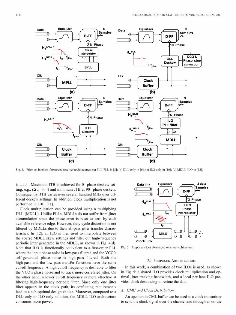
source synchronous links prefer DLLs over PLLs. For example,the QPI interface implemented in [1] uses a DLL to generatemultiple clock phases. These clock phases are distributed toeach receiver and then interpolated to generate required sam-pling phase between . Since at least four clock phases0, 90, 180, and 270 are distributed in this approach, clock dis-tribution network consumes significant power. Both the DLLand phase interpolator provide all-pass jitter transfer, so tracksboth in-phase and out-of-phase jitter. Moreover, high-frequencyjitter such as duty cycle distortion (DCD) is amplified. Thereforea DCD correction loop is often required in DLL based systems,as illustrated in Fig. 4(b) [6], [9]. Alternatively a phase filtercan be implemented by “time averaging” after the DLL whichfurther increases power consumption and complexity[1]. In ad-dition the DLL does not provide flexible clock multiplication,so a full rate clock needs to be forwarded.Injection locked oscillators (ILO) are a power- and area-ef-
ficient alternative to PLLs and DLLs. In [10], [11] an ILO per-forms both jitter filtering and clock deskew by introducing a fre-quency offset between the ILO’s free-running frequency and theinjected frequency. Note that no phase detector, charge pump orloop filter is required in this architecture. Therefore, excellentarea and power efficiency is reported in [10], [11]. However,this simple architecture, illustrated in Fig. 4(c), has several lim-itations. First, the deskew range is limited and within the deskewrange jitter tracking bandwidth varies significantly as a functionof phase deskew setting. Theoretical limit of the deskew range
1340 IEEE JOURNAL OF SOLID-STATE CIRCUITS, VOL. 46, NO. 6, JUNE 2011
Fig. 4. Prior-art in clock-forwarded receiver architectures: (a) PLL-PLL in [8]; (b) DLL only in [6]; (c) ILO only in [10]; (d) MDLL-ILO in [12].
is . Maximum JTB is achieved for 0 phase deskew set-ting, e.g., ( ) and minimum JTB at 90 phase deskew.Consequently, JTB varies over several hundred MHz over dif-ferent deskew settings. In addition, clock multiplication is notperformed in [10], [11].Clock multiplication can be provided using a multiplying
DLL (MDLL). Unlike PLLs, MDLLs do not suffer from jitteraccumulation since the phase error is reset to zero by eachavailable reference edge. However, duty cycle distortion is notfiltered by MDLLs due to their all-pass jitter transfer charac-teristics. In [12], an ILO is then used to interpolate betweenthe coarse MDLL skew settings and filter out high-frequencyperiodic jitter generated in the MDLL, as shown in Fig. 4(d).Note that ILO is functionally equivalent to a first-order PLLwhere the input phase noise is low-pass filtered and the VCO’sself-generated phase noise is high-pass filtered. Both thehigh-pass and the low-pass transfer functions have the samecut-off frequency. A high cutoff frequency is desirable to filterthe VCO’s phase noise and to track more correlated jitter. Onthe other hand, a lower cutoff frequency is more effective atfiltering high-frequency periodic jitter. Since only one jitterfilter appears in the clock path, its conflicting requirementslead to a sub-optimal design choice. Moreover, compared to aDLL-only or ILO-only solution, the MDLL-ILO architectureconsumes more power.
Fig. 5. Proposed clock forwarded receiver architecture.
IV. PROPOSED ARCHITECTURE
In this work, a combination of two ILOs is used, as shownin Fig. 5: a shared ILO provides clock multiplication and op-timal jitter tracking bandwidth, and a local per lane ILO pro-vides clock deskewing to retime the data.
A. CMU and Clock Distribution
An open drain CML buffer can be used as a clock transmitterto send the clock signal over the channel and through an on-die

HOSSAIN AND CHAN CARUSONE: 7.4 Gb/s 6.8 mW SOURCE SYNCHRONOUS RECEIVER IN 65 nm CMOS 1341
Fig. 6. (a) Passive clock distribution in a conventional clock forwarded link. (b) The proposed ILO based clock distribution. The width of and are 60 mand the width of is 30 m.
transmission line at the receiver side, as shown in Fig. 6(a). TheCML buffer needs at least 6 mA current to achieve 200 mVswing throughout the receiver. This clock distribution providesa good compromise between power consumption, latency andsupply noise rejection.The proposed architecture, shown in Fig. 6(b), makes a
simple modification to this existing clock distribution approach– a phase filter is introduced in the form of an injection lockedring VCO. A three-stage ring oscillator is used as the clockmultiplying ILO (MILO) where two stages of CML invertersare tunable delay elements. The third stage in the MILO ring isused as a clock buffer as well as providing the additional gainand delay required sustain the oscillations. The total power ofthe clock transmitter is redistributed between the open-drainclock transmitter and the MILO buffer to achieve the sameswing as before. The VCO is tunable from 1.7 to 4.5 GHzto provide a half-rate clock for 4 Gb/s to 8 Gb/s operation.Compared to existing clock distribution schemes, this ILObased clock distribution does not add any additional latencyin the clock path. The only added power consumption in theproposed architecture are the two tunable delay elements.Inductor resonates out part of the pad capacitance and
device capacitance of and forming a low (2 to 2.5) LC filter. Transistors serve as a cross-coupledcommon-gate clock buffer distributing the clock signal across 1mm of on-die transmission line to the local injection locked os-cillator (LILO). Estimated loss of this on-die transmission lineis 1.25 dB/mm. Including the low LC filter, the clock dis-tribution network suffers 3.5 to 4 dB loss at 4 GHz. Althoughnarrow band resonant clocking can provide very low powerclock distribution [8], in this work to support several data rates,a relatively low filter with broadband transmission line is pre-ferred for clock distribution [4]. In addition supply induced jitter
is minimized by using a CML style clock buffer and .The main disadvantage of this approach is the higher loss due tolower and the relative power inefficiency of the CML bufferas a clock driver. Due to the limited silicon area in the imple-mented protoype, the MILO clock buffer is driving only oneLILO and a 1 mm on-die transmission line. However, simula-tion results show that the existing MILO can drive up to fourLILO with more than 400 mVp-p differential swing. It is wellknown that injection locked oscillators are functionally equiva-lent to a first-order PLL [13]. Thus their jitter transfer functioncan be written as
(5)
where the pole of the jitter transfer function can be written as
(6)
Here, is the injection strength, captures VCOtopology dependency [14] and is the frequency differencebetween free running ILO frequency and the injected fre-quency . To accommodate clock multiplication, a subrateclock can be forwarded and the MILO tuned to lock to oneof its harmonics. For example, an ILO can provide 5 clockmultiplication when locked to the 5th harmonic of the injectedsignal as shown in Fig. 7(a). However, injection strength inthis case is determined by the amplitude of the 5th harmonicwhich is only a small fraction of the fundamental tone. Thiscan be better understood by taking the Fourier transform of thepulse train as illustrated in Fig. 8. For a given pulse amplitudeand duty cycle of 50%, the amplitude of the th harmonic is

1342 IEEE JOURNAL OF SOLID-STATE CIRCUITS, VOL. 46, NO. 6, JUNE 2011
Fig. 7. The simulated transmitted signal and MILO output in the time and fre-quency domains: (a) NRZ; (b) pulse signal. The spectra are normalized to thepower of the extracted tone at 4 GHz.
Fig. 8. Pulse train in time and frequency domain.
. Hence, to obtain sufficient locking range, a lower fre-quency pulse train requires a larger injection amplitude . Notethat although in theory the ratio between the th harmonicamplitude and the fundamental is , this ratio is reduced dueto bandwidth limitations of the circuit. For example, this ratioof approximately 1/7.5 is observed for the fifth harmonic in thespectrum plot of Fig. 7(a). As a result generally if injected witha sub rate (quarter-rate or lower) clock, significant amplitudedistortion and reference spurs appear at the MILO output.This problem is ameliorated in this work by injecting a pulse
train as shown in Fig. 7(b). The effective injection strength ofthe th harmonic of the pulse train can be obtained using theFourier series:
(7)
This is illustrated in Fig. 8. For the fundamental frequency,, the injection strength is
(8)
Similarly, for a sub-rate forwarded clock,
(9)
Assuming a 10% duty cycle, the ratio between the fifth har-monic and the fundamental is approximately 3/5. Comparedto injection of a subrate 50% duty-cycle clock, pulse injectionprovides a 3 improvement in signal to distortion ratio. Un-like NRZ signals, pulse trains effect the MILO output only attheir transitions. As a result, amplitude distortion and frequencyspurs are significantly reduced. Pulse trains are generated usinga delay and XOR gate integrated into the clock transmitter ofthis prototype link [Fig. 6(b)]. Pulse width is controlled bythe delay element, . Pseudo differential CMOS inverters areused as a pre-driver of the clock transmitter. The additionaldelay introduced by the extra inverter in the single ended todifferential converter is a small fraction of the clock period,hence negligible. Simulation results of this approach are shownin Fig. 7(b).Using expression (9) for effective injection strength, the jitter
tracking bandwidth can be written as a function of pulse repeti-tion rate, , and pulse duty cycle, :
(10)
Here, we assume negligible frequency offset ( ). Thiscan be ensured in two ways. In the first approach, a frequencycalibration loop with a replica VCO can be used for frequencytracking as reported in [15]. Since the PLL with replica VCO isalways running, supply and temperature variations are trackedand compensated by the feedback loop. The only downside isthe added power and area penalty of the extra PLL. In the secondapproach, the frequency of the free running ILO can be cal-ibrated during start up and the control voltage set such that
. In this work we used the second approach to re-duce power and complexity.TheMILO JTB is set by the effective injection strength which
is controlled by changing the duty cycle, , and pulse repetitionrate, (Fig. 9). The effect of pulse repetition rate upon trackingbandwidth is illustrated in the phase step response. The phasestep responses are generated by shifting the rising edge of theinput pulse train. As expected, with the MILO phase isupdated more frequently than with resulting in a highertracking bandwidth for than . Tracking bandwidthcan also be adjusted by adjusting the duty cycle as shown inFig. 10, thereby providing continuous adjustment of the JTBfrom 25MHz to 300MHz. The shared clock circuitry consumesmore power than any other block in the link to ensure that evenwhen set to a low JTB, a low phase noise clock is distributed tothe LILOs.

HOSSAIN AND CHAN CARUSONE: 7.4 Gb/s 6.8 mW SOURCE SYNCHRONOUS RECEIVER IN 65 nm CMOS 1343
Fig. 9. The phase step response and the corresponding jitter transfer functions for different pulse repetition rates ,2,4,8.
Fig. 10. Phase step response for different duty cycles.
B. Phase Interpolation With Injection Locking
The MILO output is distributed by a passive clock distribu-tion network. This low-power clock distribution technique pro-vides better supply rejection and lower latency than a bufferedapproach at the cost of smaller signal swing. Each lane of the re-ceiver requires a deskew circuit to provide precise phase align-ment, amplification and high-frequency jitter (DCD) filtering ofthe clock as well as generating all phases required by the sam-pling flip-flops. Two existing approaches to ILO-based clockdeskew are shown in Fig. 11(a)-(b).In [12] both 0 and 90 degree clock phases are combined to-
gether to inject symmetrically in every stage of the the ring os-cillator [Fig. 11(a)]. By adjusting the relative strength of the in-jection phase, interpolation can be obtained. This method pro-vides complete phase interpolation and JTB re-mains relatively constant over the phase interpolation range. Butdistributing quadrature phases (0 , 90 , 180 , 270 ) throughoutthe die consumes significant power. Alternatively, in [10] onlydifferential phases (0 , 180 ) are injected to a single point in theVCO [Fig. 11(b)]. As a result power consumption in the clockdistribution network in halved. Phase interpolation is then ob-tained by detuning the free running ILO frequency. However,the JTF is a strong function of the frequency offset and hencephase deskew. As a result to obtain phase shifts greater than45 , jitter tracking bandwidth significantly drops. In addition,
the phase deskew range is smaller than the previous approach.To overcome the above limitations, the proposed architecture
is shown in Fig. 11(c) combining the benefits of the above ar-
chitectures. Instead of combining four phases, we inject the dif-ferential clock into the ring at two points with adjustable po-larity and three possible injection strengths to select betweeneight coarse deskew settings, as shown in Fig. 12. Interpolationbetween these coarse settings is done by slightly detuning theLILO’s free-running frequency. The resulting phase shift, ,and the corresponding frequency offset, , are related by thefollowing expression:
(11)
For the maximum required phase shift 23 , the largest re-quired frequency offset is:
MHz. This translates to a minimum jitter tracking band-width in (6), MHz. TheLILO’s measured tracking bandwidth exceeds 600 MHz so thatthe overall JTB of the clock path is determined by the MILO,independent of the phase deskew setting. The LILO is designedto have wide tuning range (2 GHz to 5.5 GHz) to accommodatea wide range of data rates with some additional margin for finephase interpolation.
C. Phase Noise Filtering
The jitter transfer of the shared CMU and local phase inter-polator is shown in Fig. 13. The phase noise of the CMU outputcan be written as
(12)where is the jitter spectrum of the supplied reference clock,
is the jitter spectrum of the MILO when free-running(with no injection), and is the jitter tracking bandwidthof the MILO, which depends upon the injected duty cycle andpulse repetition rate. This CMU output is then filtered by the perlane LILO
(13)where is the free-running jitter spectrum of the LILO, and
is the tracking bandwidth of the LILO. This architectureprovides several advantages. Phase tracking of the two loopscan be set independently by appropriately choosing and
. Here, is chosen to optimize correlated jitter tracking,

1344 IEEE JOURNAL OF SOLID-STATE CIRCUITS, VOL. 46, NO. 6, JUNE 2011
Fig. 11. ILO based phase interpolator: (a) as in [12], (b) as in [9], (c) this work.
Fig. 12. The implemented ILO based phase interpolator. The width of is 20 m.
and provides some additional filtering of DCD andother very high-frequency (uncorrelated) jitter. In Section II itwas shown that the optimum tracking bandwidth for the clockpath varies from 25 MHz to 400 MHz. From (12) and (13) andFigs. 13–14, note that in the range ,is the dominant contributor to output phase noise, and its noise isnot correlated with that of the data. This can be a wide range offrequencies, especially when latency mismatch between clockand data is high requiring . Therefore it is crit-ical to design the MILO with low phase noise. As a result, theMILO consumes more power than any other ILO. Fortunately,the MILO’s power is amortized over all receiver lanes hencedoes not translate to a significant power penalty. On the otherhand MHz filters out up to very highfrequencies, so very little of appears in the recovered
clock jitter spectrum, . As a result, the per lane LILO can bedesigned with low power improving receiver power efficiency.Another advantage of high tracking bandwidth in the LILO isthat when used in a burst mode application, each receivers lanecan wake up very quickly. Very high-frequency jitter due toDCD and reference spurs is still attenuated by both ILOs. CMLdelay stages are used in both the MILO and LILO providinggood supply noise immunity.
V. IMPLEMENTATION AND EXPERIMENTAL RESULTS
Each receiver comprises an equalizer to compensate high-fre-quency channel and package losses followed by demultiplexer.The equalizer improves eye opening and reduces uncorrelatedpattern dependent jitter which will not be tracked by the for-warded clock path. In a relatively low loss channel, a simple

HOSSAIN AND CHAN CARUSONE: 7.4 Gb/s 6.8 mW SOURCE SYNCHRONOUS RECEIVER IN 65 nm CMOS 1345
Fig. 13. Phase noise transfer model for the two cascaded ILOs.
Fig. 14. Phase transfer and resultant Phase noise for the two cascaded ILOs.
passive equalizer can provide this functionality with excellentpower efficiency.
A. Passive Equalizer
A passive equalizer in the form of high-pass filter isused to equalize FR4 traces. The implemented equalizer circuitis shown in Fig. 15. Its transfer function is
(14)
The DC gain of the equalizer is and thehigh-frequency gain is 1. Thus the equalizer provides a boostof . The zero and pole of the equalizer can bewritten as and . In reality,the location of the pole is at a slightly lower frequency dueto the input capacitance. The choice of equalizer parameters
is driven by tradeoffs between input termination,input time constant and maximum boost. Small values ofand degrade input matching and require larger values of(hence area) to keep the zero at the same frequency. Larger
value resistors increase the input time constant. Fortunately, a1:2 demultiplexer introduces less loading than a higher orderdemultiplexer. To adjust the location of the zero for differentdata rates and channel characteristics, the capacitance canbe adjusted using switches as shown in Fig. 15(a). Channelresponses (20-inch long FR-4 trace) with and without the
Fig. 15. (a) The implemented passive equalizer and experimental setup. (b) Theequalizer frequency response for (20-inch) FR4 PCB trace with and withoutequalizer.
equalizer are shown in Fig. 15(b). Note that the packagedprototypes are connected through SMA cables, connectors andthe channel. No drilled vias, daughter card or other board edgeconnectors are used in the experimental setup. The channelmeasurements do not include the pad capacitance or I/O devicecapacitances. However, these were included in the simulatedchannel. Approximately 1 pF additional capacitance is used insimulation, accounting for the discrepancy between the simu-lated and measured channel responses in Fig. 15(b). Althoughthe passive equalizer achieves excellent power efficiency theirusefulness is limited to well behaved channels with less than10 dB loss at the Nyquist rate and relatively slow roll-off(20 dB/decade or lower). Since the passive equalizer does notprovide signal amplification, in lossy channels it can degradereceiver sensitivity. For channels with faster roll-off, it isdifficult to invert the channel response with a single zero anda single pole.
B. Experimental Results
The 4–7.4 Gb/s 65 nm CMOS receiver prototype is tested ina QFN package and operates from a 1 V supply. A die photoand power break down are shown in Fig. 16.The shared clock circuitry consumes 8 mW, the LILO phase
interpolator consumes 4.4 mW and the samplers consume2.4mW. Excluding shared clock power, each receiver consumes6.8 mW which equals 0.92 pJ/bit at 7.4 Gb/s. A demonstrationof 16 clockmultiplication is shown in Fig. 17. The delay-XORcombination generates a pulse train that in frequency domainis a series of impulses spaced 250 MHz apart [Fig. 17(a)-(b)].The MILO locks to the tone at 4 GHz and suppresses the

1346 IEEE JOURNAL OF SOLID-STATE CIRCUITS, VOL. 46, NO. 6, JUNE 2011
Fig. 16. Implemented protoype. (a) Block diagram with power breakdown.(b) Die photo of the prototype in 65 nm CMOS.
Fig. 17. Verification of 16 clock multiplication. (a) Pulse train in time do-main. (b) Pulse train in frequency domain. (c) Recovered clock in time domain(d) Recovered clock in frequency domain.
other tones due both to the inherent phase noise filtering ofthe MILO and the incorporated low Q passive resonator. Therecovered 4 GHz clock in time and frequency domain is shown
Fig. 18. Phase noise of the free running ILOs and of the recovered clock.
Fig. 19. (a) Measured deskew with coarse and fine control. (b) Four specificcoarse and fine phase settings.
in Fig. 17(c)-(d) and has 41 dBc reference spurs. Those spursadd 1.5 ps to the total jitter using the formula for spurioustonal jitter (spurious jitter ).The phase noise of the clock reference, MILO and LILO are
shown in Fig. 18. As explained in Section IV(C), the MILO’scontribution to recovered phase noise is dominant over a widerange of frequency offsets. Thus theMILOwas designed to haveat least 15 dB lower phase noise than the LILO at frequencyoffsets of 25 MHz to 1 GHz. The LILO phase noise is filteredout of the final recovered clock up to 1 GHz. Coarse and finephase interpolation with the ILO is demonstrated in Fig. 19.Coarse selections are set by the different injection locations, po-larities, and strengths while fine interpolation curves are gener-ated by detuning the free running frequency of the LILO. Thefine tuning curves each exceed the spacing between neighboringcoarse tuning settings by at least 60%. The linearity of this phase

HOSSAIN AND CHAN CARUSONE: 7.4 Gb/s 6.8 mW SOURCE SYNCHRONOUS RECEIVER IN 65 nm CMOS 1347
TABLE ICOMPARISON WITH STATE-OF-THE-ART LOW POWER CLOCK FORWARDED RECEIVERS
Fig. 20. Output phase as a function of deskew setting and the correspondingDNL at a clock frequency of 3.7 GHz (7.4 Gb/s data rate).
interpolator is shown in Fig. 20. The DNL is better than 3 ps,with discontinuities of 3 ps observed when switching fromone coarse tuning setting to another. The BER of the receiverfor a 2 1 pattern is shown in Fig. 21 as a function of deskewsetting over 5-inch FR4 interconnect. Note that due to the finiteresolution in skew settings and residual jitter in the recoveredclock the BER at 4 Gb/s does not quite reach 10 0.5.Jitter tolerance is tested at 7.4 Gb/s and plotted in Fig. 22. Jittertransfer is captured for three pulse repition rates, 1, 2, and4. In all cases measured rtesults are in good agreement withthe theory. In addition, latency mismatch between the clock anddata paths was kept low ( 2 UI) in the experimental setup. As
Fig. 21. (a) BER as a function of phase deskew at 4 Gb/s and 7.4 Gb/s over 10”and 5” FR4 traces, respectively. The BER is measured with a 2 1 pattern.(b) Half-rate recovered data. (c) Half-rate recovered clock.
a result jitter tolerance improved with increasing tracking band-width. The BER is less than 10 in the presence of 1.5 UI(peak-to-peak) sinusoidal PJ at 200 MHz. This is in addition to0.45 UI (peak-to-peak) deterministic jitter which was observeddue to the simple and, hence, imperfect passive equalization.

1348 IEEE JOURNAL OF SOLID-STATE CIRCUITS, VOL. 46, NO. 6, JUNE 2011
Fig. 22. (a) The clock path’s measured jitter transfer. (b) The correspondinglink jitter tolerance.
VI. CONCLUSION
The proposed architecture is compared with state-of-the-artreceivers in Table I. All the architecture previously described inSection III are considered in this comparison. Notice that ILObased solutions have achieved significantly better power effi-ciency than PLL or DLL based solutions. However, in otherworks they did not provide clock multiplication. The proposedsolution combines the functionality of PLL- or DLL-based so-lutions without sacrificing the excellent power- and area-effi-ciency offered by injection locking. The high-frequency jittertolerance achieved (1.5 UI at 200 MHz) is comparable to over-sampling CDRs, a significant improvement over previous low-power clock forwarded receivers.
REFERENCES[1] N. Kurd et al., “Next generation Intel® Core™micro-architecture (Ne-
halem) clocking,” IEEE J. Solid-State Circuits, pp. 1121–1129, Apr.2009.
[2] R. Schmitt, L. Hai, C. Madden, and C. Yuan, “Investigating the impactof supply noise on the jitter in gigabit I/O interfaces,” IEEE ElectricalPerformance of Electronic Packaging, pp. 189–192, Oct. 2007.
[3] E. Yeung andM. Horowitz, “A 2.4 Gb/s/pin simultaneous bidirectionalparallel link with per-pin skew compensation,” IEEE J. Solid-State Cir-cuits, vol. 35, no. 11, pp. 1628–1699, Nov. 2000.
[4] E. Prete, D. Scheideler, and A. Sanders, “A 100 mW 9.6 Gb/s trans-ceiver in 90 nm CMOS for next-generation memory interfaces,” inIEEE Int. Solid-State Circuits Conf. Dig., 2006, pp. 90–91.
[5] K. Lee et al., “A jitter tolerant 4.5 Gb/s CMOS interconnect for digitaldisplay,” in IEEE Int. Solid-State Circuits Conf. Dig., 1998, pp. 90–91.
[6] A. Agrawal, P. Hanumolu, and G. Wei, “A 8 5 Gb/s source-syn-chronous receiver with clock generator phase mismatch correction,”presented at the 2008 IEEECustom Integrated Circuits Conf., San Jose,CA, Sep. 2008.
[7] R. Kho et al., “A 75 nm 7 Gb/s/pin 1 Gb GDDR5 graphics memorydevice with bandwidth improvement techniques,” IEEE J. Solid-StateCircuits, vol. 45, no. 1, pp. 120–133, Jan. 2010.
[8] J. Poulton et al., “A 14-mw 6.25-Gb/s transceiver in 90-nm CMOS,”IEEE J. Solid-State Circuits, vol. 42, no. 12, pp. 2745–2757, Dec. 2007.
[9] F. O’Mahony et al., “A low-jitter PLL and repeaterless network for a20Gb/s link,” in IEEE Symp. VLSI Circuits Dig. Tech. Papers, 2006, p.29.
[10] F. O’mahony et al., “A 27 Gb/s forwarded clock I/O receiver using aninjection-locked LC-DCO in 45 nm CMOS,” in IEEE Int. Solid-StateCircuits Conf. Dig., 2008, p. 452.
[11] K. Hu et al., “A 0.6 mW/Gbps, 6.4–8.0 Gbps serial link receiver usinglocal injection-locked ring oscillators in 90 nmCMOS,” in IEEE Symp.VLSI Circuits Dig. Tech. Papers, 2009, pp. 46–47.
[12] H. Ng et al., “A second-order semidigital clock recovery circuit basedon injection locking,” IEEE J. Solid-State Circuits, vol. 38, no. 12, pp.2101–2110, Dec. 2003.
[13] R. Adler, “A study of locking phenomena in oscillators,” Proc. IRE,vol. 33, pp. 351–357, Jun. 1946.
[14] M. Hossain and A. Chan Carusone, “CMOS oscillators for clock dis-tribution and injection-locked deskew,” IEEE J. Solid-State Circuits,vol. 44, no. 8, pp. 2138–2153, Aug. 2009.
[15] F. O’Mahoney, B. Casper, M. Mansuri, and M. Hossain, “A pro-grammable phase rotator based on time-modulated injection-locking,”in IEEE Symp. VLSI Circuits Dig. Tech. Papers, 2010, pp. 45–46.
Masum Hossain (M’11) received the B.Sc. degreein electrical engineering from the Bangladesh Uni-versity of Engineering and Technology, Bangladesh,and the M.Sc. degree from Queen’s University,Canada, in 2002 and 2005, respectively. During hisM.Sc. work, he worked on K-band wireless receiverin CMOS. Since 2005, he has been working towardsthe Ph.D. degree in electrical engineering at theUniversity of Toronto, Canada.From September 2007 to January 2008, he was
with Intel Circuit Research Lab (CRL) as a graduateintern. From 2008 to 2010 he was with Gennum Corp. in the Analog and MixedSignal division. Currently, he is a senior member of technical staff at RambusLab. His research interests include mixed-signal circuits for high-speedchip-to-chip communications, low-power VCO, phase interpolator and clockrecovery techniques.Mr. Hossain won the best student paper award at the 2008 IEEE Custom
Integrated Circuits (CICC) Conference.
Anthony Chan Carusone (S’96–M’02–SM’08)received the Ph.D. degree from the University ofToronto, Canada, in 2002.Since 2001 he has been with the Department of
Electrical and Computer Engineering at the Univer-sity of Toronto where he is currently an AssociateProfessor. In 2008 he was a visiting researcher at theUniversity of Pavia, Italy, and later at the CircuitsResearch Lab of Intel Corp., Hillsboro, Oregon.He is also an occasional consultant to industry inthe areas of integrated circuit design, clocking, and
digital communication.Prof. Chan Carusone was a co-author of the best student papers at both the
2007 and 2008 Custom Integrated Circuits Conferences and the best paper atthe 2005 Compound Semiconductor Integrated Circuits Symposium. He is anappointed member of the Administrative Committee of the IEEE Solid-StateCircuits Society and sits on the Executive Committee of the Circuits and Sys-tems Society’s Board of Governors. He served on technical program committeefor the IEEE Custom Integrated Circuits Conference, and is currently a memberof the technical program committee for the VLSI Circuits Symposium. He hasserved as a guest editor for the IEEETRANSACTIONS ONCIRCUITS AND SYSTEMSI: REGULAR PAPERS and was on the editorial board of the IEEE TRANSACTIONSON CIRCUITS AND SYSTEMS II: EXPRESS BRIEFS from 2006 until 2009 when hewas Editor-in-Chief. He is currently an associate editor of the IEEE JOURNALOF SOLID-STATE CIRCUITS.