ieee journal of solid-state circuits, vol. …spalermo/ecen689/16g_vcsel_xcvr...ifornia institute of...
TRANSCRIPT
IEEE JOURNAL OF SOLID-STATE CIRCUITS, VOL. 43, NO. 5, MAY 2008 1235
A 90 nm CMOS 16 Gb/s Transceiverfor Optical Interconnects
Samuel Palermo, Member, IEEE, Azita Emami-Neyestanak, Member, IEEE, and Mark Horowitz, Fellow, IEEE
Abstract—Interconnect architectures which leverage high-band-width optical channels offer a promising solution to address theincreasing chip-to-chip I/O bandwidth demands. This paperdescribes a dense, high-speed, and low-power CMOS optical in-terconnect transceiver architecture. Vertical-cavity surface-emit-ting laser (VCSEL) data rate is extended for a given averagecurrent and corresponding reliability level with a four-tap cur-rent summing FIR transmitter. A low-voltage integrating anddouble-sampling optical receiver front-end provides adequate sen-sitivity in a power efficient manner by avoiding linear high-gainelements common in conventional transimpedance-amplifier(TIA) receivers. Clock recovery is performed with a dual-looparchitecture which employs baud-rate phase detection and feed-back interpolation to achieve reduced power consumption, whilehigh-precision phase spacing is ensured at both the transmitterand receiver through adjustable delay clock buffers. A prototypechip fabricated in 1 V 90 nm CMOS achieves 16 Gb/s operationwhile consuming 129 mW and occupying 0.105 mm�.
Index Terms—Clock and data recovery, equalization, laserdriver, optical interconnects, optical receiver, serial transceiver,VCSEL.
I. INTRODUCTION
I NTEGRATED circuit scaling has enabled a huge growthin processing power which necessitates a corresponding
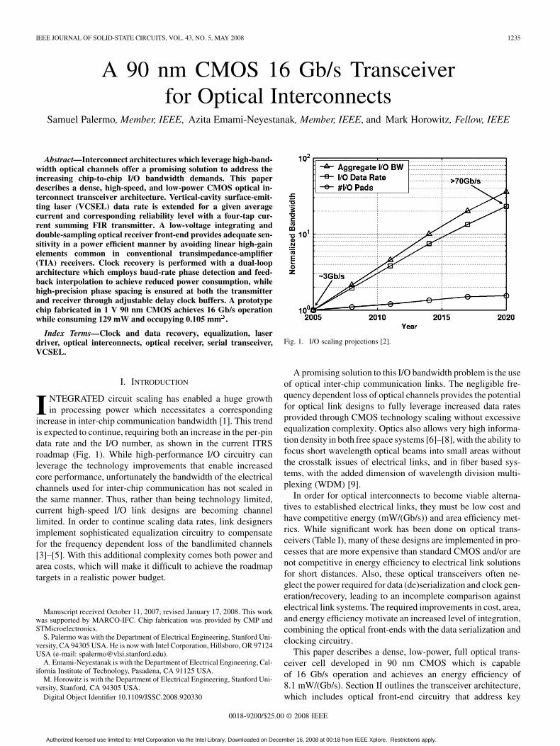
increase in inter-chip communication bandwidth [1]. This trendis expected to continue, requiring both an increase in the per-pindata rate and the I/O number, as shown in the current ITRSroadmap (Fig. 1). While high-performance I/O circuitry canleverage the technology improvements that enable increasedcore performance, unfortunately the bandwidth of the electricalchannels used for inter-chip communication has not scaled inthe same manner. Thus, rather than being technology limited,current high-speed I/O link designs are becoming channellimited. In order to continue scaling data rates, link designersimplement sophisticated equalization circuitry to compensatefor the frequency dependent loss of the bandlimited channels[3]–[5]. With this additional complexity comes both power andarea costs, which will make it difficult to achieve the roadmaptargets in a realistic power budget.
Manuscript received October 11, 2007; revised January 17, 2008. This workwas supported by MARCO-IFC. Chip fabrication was provided by CMP andSTMicroelectronics.
S. Palermo was with the Department of Electrical Engineering, Stanford Uni-versity, CA 94305 USA. He is now with Intel Corporation, Hillsboro, OR 97124USA (e-mail: [email protected]).
A. Emami-Neyestanak is with the Department of Electrical Engineering, Cal-ifornia Institute of Technology, Pasadena, CA 91125 USA.
M. Horowitz is with the Department of Electrical Engineering, Stanford Uni-versity, Stanford, CA 94305 USA.
Digital Object Identifier 10.1109/JSSC.2008.920330
Fig. 1. I/O scaling projections [2].
A promising solution to this I/O bandwidth problem is the useof optical inter-chip communication links. The negligible fre-quency dependent loss of optical channels provides the potentialfor optical link designs to fully leverage increased data ratesprovided through CMOS technology scaling without excessiveequalization complexity. Optics also allows very high informa-tion density in both free space systems [6]–[8], with the ability tofocus short wavelength optical beams into small areas withoutthe crosstalk issues of electrical links, and in fiber based sys-tems, with the added dimension of wavelength division multi-plexing (WDM) [9].
In order for optical interconnects to become viable alterna-tives to established electrical links, they must be low cost andhave competitive energy (mW/(Gb/s)) and area efficiency met-rics. While significant work has been done on optical trans-ceivers (Table I), many of these designs are implemented in pro-cesses that are more expensive than standard CMOS and/or arenot competitive in energy efficiency to electrical link solutionsfor short distances. Also, these optical transceivers often ne-glect the power required for data (de)serialization and clock gen-eration/recovery, leading to an incomplete comparison againstelectrical link systems. The required improvements in cost, area,and energy efficiency motivate an increased level of integration,combining the optical front-ends with the data serialization andclocking circuitry.
This paper describes a dense, low-power, full optical trans-ceiver cell developed in 90 nm CMOS which is capableof 16 Gb/s operation and achieves an energy efficiency of8.1 mW/(Gb/s). Section II outlines the transceiver architecture,which includes optical front-end circuitry that address key
0018-9200/$25.00 © 2008 IEEE
Authorized licensed use limited to: Intel Corporation via the Intel Library. Downloaded on December 16, 2008 at 00:18 from IEEE Xplore. Restrictions apply.

1236 IEEE JOURNAL OF SOLID-STATE CIRCUITS, VOL. 43, NO. 5, MAY 2008
TABLE IOPTICAL TRANSCEIVER PERFORMANCE COMPARISON
issues associated with vertical cavity surface-emitting laser(VCSEL) bandwidth and reliability tradeoffs and achieving ade-quate receiver sensitivity in low-voltage CMOS. A presentationof a four-tap current summing FIR transmitter which extendsVCSEL data rate for a given average current and correspondingreliability level follows in Section III. Section IV discusses anintegrating and double-sampling optical receiver architecture[17] which enables low-voltage operation suitable for modernand future CMOS technologies. A description of the clockgeneration and recovery circuitry which produces low-noiseclocks with the high-precision phase spacing required by thetime-division multiplexing architecture is given in Section V.Section VI details the full transceiver experimental results,and Section VII summarizes the work with a comparison tostate-of-the-art electrical links.
II. TRANSCEIVER ARCHITECTURE
The optical interconnect transceiver architecture is shown inFig. 2 [18]. In order to enable short bit periods without con-suming excessive area and power in clock generation and dis-tribution, multiple clock phases are employed to create a mul-tiplexing architecture at both the transmitter and receiver. Atthe transmitter side, a supply-regulated ring oscillator is usedin the frequency synthesis phase-locked loop (PLL) [19] to pro-vide five sets of complementary clock phases spaced a bit pe-riod apart which switch a five-to-one multiplexer. This allowsa 16 Gb/s serial data stream to be produced with only 3.2 GHzclock phases. The multiplexer serial output is buffered by theVCSEL driver output stage [20], which consists of a four-tapcurrent-mode FIR filter that equalizes the VCSEL response athigh data rates. At the receiver side, a low-voltage integratingand double-sampling front-end performs data demultiplexingdirectly at the input node using five uniform clock phases fromthe clock and data recovery (CDR) system. Clock recovery isperformed with a dual-loop architecture which employs baud-rate phase detection and feedback interpolation to achieve re-duced power consumption. High-precision phase spacing is en-sured at both the transmitter and receiver through adjustabledelay clock buffers applied independently on a per-phase basisthat compensates for circuit and interconnect mismatches.
III. VCSEL TRANSMITTER
Total VCSEL bandwidth is limited by a combination of elec-trical parasitics and the electron–photon interaction dynamics.The laser diode’s dominant electrical time constant comes from
the bias-dependent junction RC, with the dominant junctioncapacitor value typically between 0.5–1 pF for 10 Gb/s class850 nm VCSELs [21], [22]. In addition to the bias-dependentjunction resistance, there is also significant series resistancedue to the large number of distributed Bragg reflector (DBR)mirrors used for high reflectivity, with a total device seriesresistance typically between 50 to 150 .
VCSEL optical bandwidth is regulated by two coupled differ-ential equations which describe the electron–photon interaction[23]. Derived from these rate equations, the VCSEL relaxationoscillation frequency , which is proportional to the effectivebandwidth, is directly proportional to the square root of the in-jected current above the threshold current
(1)
Combining an electrical parasitic model with the optical rate-equation model yields the total frequency response of a 10 Gb/sclass VCSEL, shown in Fig. 3 [22].
Output power saturation due to self-heating [24] and also de-vice lifetime concerns [25] restrict excessive increase of VCSELaverage current levels to achieve higher bandwidth. VCSEL reli-ability potentially poses a series impediment to very high-speedmodulation, as the mean time to failure (MTTF) is
(2)
where is a proportionality constant dependent on the type ofinterconnect, is device current density, is the activationenergy (typically 0.7 eV), and is the junction temperature[26].
The conflicting dependencies of VCSEL bandwidth and reli-ability on device current yield the following steep tradeoff:
(3)
Thus, in order to ease this tradeoff, an equalizing FIR outputstage is used to extend the data rate for a given average current.While the VCSEL’s varying frequency response with currentlimits the performance of a linear equalizer for large signalmodulation, the frequency response variations diminish withincreasing average current due to the square root relationshipand a linear equalizer is effective in canceling intersymbolinterference (ISI).
Fig. 4(a) shows the VCSEL transmitter with a four-tap equal-izer consisting of one pre-cursor, one main, and two post-cursor
Authorized licensed use limited to: Intel Corporation via the Intel Library. Downloaded on December 16, 2008 at 00:18 from IEEE Xplore. Restrictions apply.

PALERMO et al.: A 90 nm CMOS 16 Gb/s TRANSCEIVER FOR OPTICAL INTERCONNECTS 1237
Fig. 2. Optical transceiver architecture.
Fig. 3. Modeled 10 Gb/s class VCSEL frequency response [22].
taps implemented by summing current sources at the outputnode. Five parallel data bits, [4:0], are routed to the taps,where they are shifted one bit time with respect to the clockphases to implement the necessary filter delays. At each tap, apseudo-differential multiplexer serializes the five parallel inputbits and drives a differential output stage which steers currentbetween the VCSEL and dummy diode-connected thick-oxidenMOS devices that are connected to a separate 2.8 Vsupply. This higher supply is necessary to support the 1.5 VVCSEL knee voltage. A static DC current source, , is also
used to bias the VCSEL above the threshold current to insureadequate bandwidth. This bias current and the leakage currentfrom the tap driver transistors, , provide sufficient voltagedrop across the VCSEL and dummy load to prevent excessivevoltage stress on the output stage transistors.
As shown in Fig. 4(b), at each tap the five two-transistor mul-tiplexing segments are switched with pairs of complementaryclock phases spaced a bit time apart in order to form a currentpulse that defines the data bit. Tunable delay predrivers, whichcompensate for clock static phase offsets and duty cycle errors,qualify the clocks with the data and provide buffering to drivethe multiplexing segments. Eight-bit current mirror DACs biasthe output stages to the desired current value. Because of thesmaller current requirements of the pre/post-cursor taps, theirmuxes and output stages are set to one-fourth the size of themain tap to save power.
Fig. 5 shows measured optical eye diagrams at 16 Gb/s froma 10 Gb/s-class commercial VCSEL with an average current of6.2 mA and a 3 dB extinction ratio. The four-tap equalizationimproves vertical eye opening by 45% while maintaining thesame average operating current, and thus the same level ofVCSEL reliability. While optimizing the equalizer tap valuesfor maximum vertical eye opening resulted in overall improvedlink margin, the symbol-spaced equalization does introduceslightly more jitter ( 8% UI). It is possible to reduce this jitterat the expense of vertical eye opening improvement by adjustingthe symbol-spaced tap values to co-optimize for both horizontaland vertical eye opening. While further improvement is possibleby altering the architecture to include half-symbol-spaced taps
Authorized licensed use limited to: Intel Corporation via the Intel Library. Downloaded on December 16, 2008 at 00:18 from IEEE Xplore. Restrictions apply.

1238 IEEE JOURNAL OF SOLID-STATE CIRCUITS, VOL. 43, NO. 5, MAY 2008
Fig. 4. VCSEL transmitter. (a) Four-tap equalizer. (b) Tap multiplexer and output stage schematic.
dedicated to canceling edge ISI, this was deemed not worthy ofthe additional equalization complexity and power consumption.
The maximum data rate (minimum 80% vertical eye opening)versus average VCSEL current with and without equalization isshown in Fig. 6. At 14 Gbps, equalization allows the VCSELto run at 35% less average current, which due to the fourth-order power dependence results in a potential 138% increasein VCSEL lifetime. The four-tap equalization extends the max-imum data rate from 14 to 18 Gbps before exceeding driver cur-rent levels.
IV. OPTICAL RECEIVER
In traditional optical receiver front-ends, a transimpedanceamplifier (TIA) converts the photocurrent into a voltage andis followed by limiting amplifier stages which provide am-plification to levels sufficient to drive a high-speed latch fordata recovery. Excellent sensitivity and high bandwidth canbe achieved by TIAs that use a negative feedback amplifier toreduce the input time constant [11], [13], [27]. Unfortunately,
while process scaling has been beneficial to digital circuitry, ithas adversely affected analog parameters such as output resis-tance which is critical to amplifier gain. Another issue arisesfrom the inherent transimpedance limit [28], which requiresthe gain–bandwidth of the internal amplifiers used in TIAsto increase as a quadratic function of the required bandwidthin order to maintain the same effective transimpedance gain.While the use of peaking inductors can allow bandwidth exten-sion for a given power consumption [27], [28], these high-areapassives lead to increased chip costs. These scaling trends havereduced TIA efficiency, thereby requiring an increasing numberof limiting amplifier stages in the receiver front-end to achievea given sensitivity and leading to excessive power and areaconsumption.
A receiver front-end architecture that eliminates linear high-gain elements, and thus is less sensitive to the reduced gainin modern processes, is the integrating and double-samplingfront-end developed by Emami [17]. The absence of high-gainamplifiers allows for savings in both power and area and makesthe integrating and double-sampling architecture advantageous
Authorized licensed use limited to: Intel Corporation via the Intel Library. Downloaded on December 16, 2008 at 00:18 from IEEE Xplore. Restrictions apply.

PALERMO et al.: A 90 nm CMOS 16 Gb/s TRANSCEIVER FOR OPTICAL INTERCONNECTS 1239
Fig. 5. 16 Gb/s optical eye diagrams from four-tap VCSEL TX.
Fig. 6. VCSEL transmitter maximum data rate versus average current.
for chip-to-chip optical interconnect systems where retiming isalso performed at the receiver.
The integrating and double-sampling receiver front-end,shown in Fig. 7, demultiplexes the incoming data stream withfive parallel segments that include a pair of input samplers, abuffer, and a sense amplifier. Two current sources at the receiverinput node, the photodiode current and a current source thatis feedback biased to the average photodiode current, supplyand deplete charge from the receiver input capacitance, respec-tively. For data encoded to ensure DC balance, the input voltage
will integrate up or down due to the mismatch in these currents.A differential voltage, , that represents the polarity of thereceived bit is developed by sampling the input voltage at thebeginning and end of a bit period defined by the rising edgesof the synchronized sampling clocks and thatare spaced a bit-period, , apart. This differential voltage isbuffered and applied to the inputs of an offset-corrected senseamplifier [29] which is used to regenerate the signal to CMOSlevels.
The use of multiple receiver segments clocked with multiplesampling phases spaced a bit period apart allows for demulti-plexing of the serial data stream directly at the input node. Inputdemultiplexing provides an increase in the achievable data rateby reducing the receiver clocks frequency and the individual re-ceiver segments bandwidth by the demultiplexing factor. Whileone receiver segment is in sampling mode, the sense amplifiersin the other receiver segments have time to resolve the data andpre-charge, allowing for continuous data resolution. As in thetransmitter, a demuliplexing factor of five is used.
While in a previous implementation [17] was applieddirectly to the sense amplifier for data regeneration, the reducedsupply voltage that comes with modern CMOS technologiescauses the integrating input to exceed the sense-amp inputrange. In order to fix the sense amplifier common-mode inputlevel and buffer the sensitive sample nodes from kickbackcharge, a differential buffer is inserted between the samplersand the sense-amp. The power penalty of the additional bufferis quite small (250 per segment), as buffer gain is low toavoid sense amplifier offset saturation and bandwidth require-ments are relaxed due to input demultiplexing.
Due to the front-end’s integrating nature, the receiversensitivity is a strong function of the bit period, total inputcapacitance , and photodiode responsivity, . The receiversensitivity can be expressed as
(4)
where is the minimum average optical power that generatesthe integrating current per bit sufficient for a given bit errorrate (BER).
The input capacitance consists of
(5)
where is the photodetector capacitance, is the inputinterconnect capacitance, is the demultiplexing factor (5), and
is the total hold capacitance for each sampler. Note that whileonly half the samplers are active at one time, (5) includes thefactor of which accounts for the equal number of phasesamplers required for the clock recovery system discussed inSection V.
The required is set by input referring the sum of theresidual sense amplifier offset after correction, , and thevoltage necessary for the sense amplifier to correctly resolveat a given data rate, . In addition, a minimum signal-to-noise ratio (SNR) must be maintained in order to achieve a givenBER and the interference associated with the average current
Authorized licensed use limited to: Intel Corporation via the Intel Library. Downloaded on December 16, 2008 at 00:18 from IEEE Xplore. Restrictions apply.

1240 IEEE JOURNAL OF SOLID-STATE CIRCUITS, VOL. 43, NO. 5, MAY 2008
Fig. 7. Integrating and double-sampling receiver front-end.
variation, , must be accounted. Combining these termsresults in a total minimum voltage swing per bit of
(6)
where is the total input voltage noise variance which is com-puted by input referring the receiver segment circuit noise andthe effective clock jitter noise.
Contributing to the input referred circuit noise are the senseamplifier, buffer, and samplers in the receiver segments. Thesense amplifier is modeled as a sampler with gain and has aninput referred voltage noise variance of
(7)
Here is the internal sense amplifier node capacitance whichis set to approximately 40 fF in order to obtain sufficient offsetcorrection range. The sense amplifier gain, , is estimated tobe equal to near unity for the 0.9 V common-mode input levelset by the buffer output, resulting in a sense amplifier voltagenoise sigma of 0.45 mV . Buffer input referred voltage noisevariance is equal to
(8)
where and are the input nMOS excess noise coefficientand transconductance, is the resistor load, and is the
noise bandwidth. A 250 A tail current provides sufficient tran-sistor transconductance to achieve a buffer voltage noise sigmaof 1.03 mV and a bandwidth of 14 GHz. Sampler voltagenoise variance is equal to
(9)
where the factor of two is due to the receiver segments’ double-samplers which generate the differential input voltage to thebuffer. Here is approximately 10 fF, with 55% due to thebuffer input capacitance and 45% due to sampler and intercon-nect capacitance. This results in an input sampler voltage noisesigma of 0.92 mV .
Clock jitter also has an impact on the receiver sensitivity be-cause any deviations from the ideal sampling time results in areduced double-sampled differential voltage. This timing inac-curacy is mapped into an effective voltage noise on the inte-grated input signal with a variance of
(10)
which, using the measured clock jitter, is estimated at0.65 mV . Combining the input referred circuit noiseand effective clock jitter noise
(11)
results in a total input noise sigma of 1.59 mV .
Authorized licensed use limited to: Intel Corporation via the Intel Library. Downloaded on December 16, 2008 at 00:18 from IEEE Xplore. Restrictions apply.

PALERMO et al.: A 90 nm CMOS 16 Gb/s TRANSCEIVER FOR OPTICAL INTERCONNECTS 1241
Fig. 8. Sense amplifier with capacitive offset correction.
In order for the receiver to achieve adequate sensitivity,it is essential to minimize the sense amplifier input-referredoffset caused by device and capacitive mismatches. While theinput-referred offset can be compensated by increasing thetotal area of the sense amplifier [30], this reduces sensitivity byincreasing input capacitance and also results in higher powerconsumption. Thus, in order to minimize the input-referredoffset while still using relatively small devices, a capacitivetrimming offset correction technique is used [31]. As shownin Fig. 8, digitally adjustable pMOS capacitors attached tointernal nodes and cause the two nodes to discharge atdifferent rates and modify the effective input voltage, ,to the positive-feedback stage. Using this technique, an offsetcorrection range of 70 mV with a residual of 1.15 mVis achieved. The fixed input common-mode voltage providedby the segment buffers eliminates variability in the offset cor-rection magnitude as the input signal integrates over the inputvoltage range.
The average current variation is limited to less than 5% withfrequency content corresponding to 8B/10B encoded data. As-suming that is made negligible with adequate sense am-plifier regeneration time, a mV is required for a
, which results in an estimatedreceiver sensitivity of 9.8 dBm at 10 Gb/s with a total input ca-pacitance of 440 fF and a photodetector responsivity of 0.5 A/W.
A wide input voltage range is necessary to maintain adequatereceiver dynamic range. Improvements in the dynamic rangerelative to the original implementation [17] are enabled throughthe use of pMOS input samplers and by the additional buffersfixing the sense amplifier input voltage independent of the inputand thus eliminating offset correction variability. The maximumreceiver input voltage is limited to approximately 1.1 V due toincomplete sampler turn-off and excessive leakage corruptingthe sampled value, while the input voltage can drop to 0.6 Vbefore the segment buffers drop into low-bandwidth regions.
V. CLOCK RECOVERY AND PER-PHASE ADJUSTMENT
A conventional dual-loop CDR [32], with a frequencysynthesis loop and a secondary phase interpolating loop, canachieve high performance from the flexibility to optimize boththe frequency synthesis loop bandwidth to filter VCO jitter andthe phase loop bandwidth to reduce jitter transfer from the noisyinput signal. However, using a straight dual-loop CDR in an
Fig. 9. Dual-loop CDR with feedback interpolation.
input demultiplexing receiver can be costly in terms of area andpower, as the number of phase muxes and interpolaters equalsthe demultiplexing factor. In this receiver implementation, fivephase muxes and interpolators are required.
A more power-efficient CDR architecture is inspired by thework of Larsson [33], who proposed placing an interpolator inthe feedback divide path of a PLL in order to filter large outputphase jumps that occur with the switching of the interpolatorphase positions. When this concept is extended to the input de-multiplexing receiver, as shown in Fig. 9 [18], the phase posi-tion of all the VCO output clocks are simultaneously adjustedwith only one phase-mux/interpolator pair allowing for signif-icant power and area savings. An additional advantage of thisarchitecture is that the clock paths from the VCO to the inputdata and phase samplers are now minimized, resulting in re-duced jitter accumulation. Also, the static clock paths allowsfor any VCO and clock distribution phase errors to be tuned outwith a low-bandwidth control loop.
One issue with this feedback interpolation architecture is thatnow the frequency synthesis and phase tracking loops are cou-pled and care must be taken in setting the two loop bandwidthsin order to ensure system stability. Whenever the phase recoveryloop state machine updates the interpolator settings, the timefor the update to be seen by the phase detector is dominatedby the PLL frequency synthesis loop settling time. Thus, thebandwidth of the phase recovery loop must be much less thanthe frequency synthesis loop to avoid excessive dithering in thereceiver clocks. Interestingly, this coincides with the filteringrequired for VCO noise and input jitter transfer suppression.The frequency synthesis loop bandwidth is set relatively high at1/20th the input reference clock frequency to filter phase noisefrom the ring oscillator and allow the PLL to track the CDR up-dates, while the secondary phase loop update rate is set roughlyan order of magnitude lower to suppress input jitter transfer.While a low phase update rate can reduce the CDR frequencytracking range, a potential solution to this is to modify the phasetracking loop to a second-order loop [34] to allow for higherppm differences between transmit and receive clocks.
The integrating front-end allows for the efficient implemen-tation of baud-rate phase detection [35]. In order to minimize
Authorized licensed use limited to: Intel Corporation via the Intel Library. Downloaded on December 16, 2008 at 00:18 from IEEE Xplore. Restrictions apply.

1242 IEEE JOURNAL OF SOLID-STATE CIRCUITS, VOL. 43, NO. 5, MAY 2008
Fig. 10. Input voltage waveform with baud-rate phase detection [35].
timing offsets, a phase detector consisting of the main data re-ceiver segments and identical phase receiver segments is imple-mented (Fig. 2). The baud-rate technique uses the same data de-tection samples for phase detection, with a digital phase signal
produced by comparing samples separated by two bitperiods, and . As shown in Fig. 10, valid phase in-formation is extracted for certain four-bit patterns that containa middle transition and a maximum of one additional transi-tion. The main advantage of baud-rate phase detection is thatno quadrature (1/2 UI) phases are required. This saves powerand area by reducing the number of distributed clock phases bya factor of two when compared to conventional 2 oversam-pling phase detection. Also, because the same samples are usedfor both data and phase detection, this architecture is less sen-sitive to clock phase errors. The primary disadvantage is that itreduces the net update rate to 18.75% for random data due toincomplete phase information with some data patterns.
CDR performance is verified in Fig. 11, which shows receiverclock waveforms at 3.2 GHz, corresponding to a 16 Gb/s datarate. When CDR tracking is disabled, the output jitter is only afunction of the frequency synthesis PLL which has 1.74 psjitter. When the CDR is activated to lock onto incoming data, theclock jitter increases only marginally to 1.90 ps , implyingthat the CDR provides sufficient filtering of input noise.
Guaranteeing precise clock phase spacing at the criticalpoints of transmitter multiplexing and receiver demultiplexingis required to ensure adequate link timing margins. Achievingthis accuracy is nontrivial due to static phase errors that formin the clock generation and distribution circuitry from bothsystematic loading imbalances and random mismatches in theVCO, distribution buffers, and interconnect. In this design,
clock phase correction is achieved through adjustable delaybuffers with digitally controlled capacitive loads, shown inFig. 12. As the tuning switches are activated, longer buffer de-lays occur due to the increased node capacitance. A mixture ofboth nMOS and pMOS switched capacitors is used to provideuniform rising and falling-edge delay adjustment. An exampleof the per-phase clock correction performance is shown withthe measured phase offsets of the five 3.2 GHz receiver clocksin Fig. 13. The uncorrected clocks have phase errors that exceed10% of the 16 Gb/s UI. These phase errors are reduced to within2%UI when the per-phase correction is enabled.
VI. EXPERIMENTAL RESULTS
The optical transceiver was fabricated in a 90 nm standardCMOS process. Both the 850 nm VCSEL and photodetectorare attached with short wirebonds, as shown in Fig. 14. TheVCSEL output beam is free-space imaged to the receiver boardand focused on a photodiode via a system of lenses.
Proper operation of the low-voltage integrating anddouble-sampling receiver is verified by observing the re-ceiver input integrating node response to a 10 Gb/s 20 bitrepeating data pattern obtained with on-die subsamplers, shownin Fig. 15. Receiver sensitivity, plotted in Fig. 16, was measuredfor both 8B/10B data patterns and also longer runlength datawith a maximum variance of 10 bits in order to further stressthe integrating receiver. Due to the integrating nature of thefront-end, the required optical power increases roughly linearlyfrom 5 to 14 Gb/s, with a sensitivity of 9.6 dBm at 10 Gb/sfor a BER of 10 . At higher data rates, the required opticalpower increases at a greater rate primarily due to increasedISI from reflections associated with the photodiode wirebond
Authorized licensed use limited to: Intel Corporation via the Intel Library. Downloaded on December 16, 2008 at 00:18 from IEEE Xplore. Restrictions apply.

PALERMO et al.: A 90 nm CMOS 16 Gb/s TRANSCEIVER FOR OPTICAL INTERCONNECTS 1243
Fig. 11. Clock jitter performance. (a) Frequency synthesis PLL. (b) CDR re-covered clock.
Fig. 12. Adjustable delay clock buffer.
connection. A sensitivity of 5.4 dBm is achieved at themaximum data rate of 16 Gb/s. When the 4.8 dB power penaltyfrom the finite transmit extinction ratio is subtracted from themaximum 3.1 dBm average transmit power, this results in amargin of 7.9 dB at 10 Gb/s and 3.7 dB at 16 Gb/s to accountfor additional link losses and noise sources. It is worth notingthat with a more integrated approach, such as flip-chip bondingthe photodiodes, superior sensitivity numbers could be achieveddue to the minimization of the inductive bondwire parasiticsthat degrade the ideally capacitive receiver input impedance.Using the measured receiver sensitivity, the integrating receiver
Fig. 13. Receiver clock phase correction performance.
Fig. 14. Micrograph of optical transceiver with bonded VCSEL and opticalreceiver with bonded photodiode.
can potentially handle runlengths of up to 40 bits at 10 Gb/sand 24 bits at 16 Gb/s. In 8B/10B data systems, the receiver hasan estimated dynamic range of 8.2 dB at 10 Gb/s and 6.1 dB at16 Gb/s.
Transceiver power consumption versus data rate is shownin Fig. 17. The power consumption scales nearly linearlywith the data rate. This is mainly due to the large percentageof CMOS-style circuitry used in both transmitters and thein receiver. Also, as data rates are lowered the integratingreceiver sensitivity improves, allowing for reduced transmitpower or VCSEL current. At 16 Gb/s, the power is 129 mWor 8.1 mW/Gb/s. The transceiver power breakdown in Fig. 18shows that 45% of the power is consumed in the receiver and55% in the transmitter.
Table II summarizes the transceiver performance. Thetransceiver operates at a data rate of 5 to 16 Gb/s, with a nom-inal transmit extinction ratio of 3 dB and a maximum averageoptical launch power of 3.1 dBm. Total transceiver area is0.105 mm .
Authorized licensed use limited to: Intel Corporation via the Intel Library. Downloaded on December 16, 2008 at 00:18 from IEEE Xplore. Restrictions apply.

1244 IEEE JOURNAL OF SOLID-STATE CIRCUITS, VOL. 43, NO. 5, MAY 2008
Fig. 15. Integrating receiver input node response to a 10 Gb/s 20 bit repeatingpattern. Note from the on-die measurement, bits 3 and 13 are somewhat distorteddue to periodic noise on the subsamplers supply that is believed to not be presenton the input waveform.
Fig. 16. Measured integrating receiver sensitivity versus data rate.
Fig. 17. Optical transceiver power versus data rate.
VII. CONCLUSION
This paper presented a power-efficient optical transceiver ar-chitecture which achieves high data rates and addresses issuesin reliably driving optical VCSELs and low-voltage optical re-ceiver design. The VCSEL driver eases the tradeoff betweenVCSEL bandwidth and reliability by employing simple trans-mitter equalization techniques in order to extend the effective
Fig. 18. Optical transceiver power breakdown at 16 Gb/s.
TABLE IITRANSCEIVER PERFORMANCE SUMMARY
device bandwidth at a given average current and correspondingreliability level. An improved low-voltage integrating receiverprovides adequate sensitivity in a power efficient manner byavoiding the use of linear high-gain elements whose efficiencyis degraded with the reduction in both voltage headroom and in-trinsic device gain associated with CMOS scaling. Further im-provements in power efficiency are realized with a clock re-covery system which employs baud-rate phase detection andfeedback interpolation. At both the transmitter and receiver, ad-justable delay clock buffers are applied independently on a per-phase basis to ensure high-precision phase spacing at the critical(de)multiplexing points.
Fig. 19 compares the energy efficiency and area performanceof the optical transceiver with state-of-the-art electrical links.The optical link compares favorably due to the use of only verysimple transmitter equalization. Conversely, the majority of theelectrical links employ both transmitter equalization and eitheranalog or sophisticated decision feedback equalization at the re-ceiver. While there has been recent work on reducing link power
Authorized licensed use limited to: Intel Corporation via the Intel Library. Downloaded on December 16, 2008 at 00:18 from IEEE Xplore. Restrictions apply.

PALERMO et al.: A 90 nm CMOS 16 Gb/s TRANSCEIVER FOR OPTICAL INTERCONNECTS 1245
Fig. 19. Optical versus electrical transceiver performance comparisons. (a) En-ergy efficiency. (b) Circuit area.
[36], [37], these implementations have focused on moderatedata rates over refined channels. In order to meet future systembandwidth demands, this approach will require extremely denseI/O architectures over optimized electrical channels that will ul-timately be limited by the chip bump/pad pitch and crosstalkconstraints.
The relative performance should scale well for the opticallink with improved optical devices. VCSEL technology con-tinues to evolve, with higher bandwidths [38], reduced thresholdcurrents [39], and the development of longer wavelength de-vices [40] allowing for reduced forward voltages and link budgetimprovements due to correspondingly less fiber loss and im-proved photodetector responsivity. In addition, advances madein photodetectors [41], [42] allow for high responsivity at lowcapacitance, resulting in improved optical receiver sensitivity.In contrast, increased system bandwidth demands even moreequalization and/or modulation complexity from electrical links
in order to signal at higher data rates over the bandlimited elec-trical channels.
ACKNOWLEDGMENT
The authors would like to acknowledge the help and supportof D. Patil, B. Nezamfar, P. Chiang, and B. Gupta, CMPand STMicroelectronics for chip fabrication, ULM photonicsfor VCSELs, Albis Optoelectronics for photodiodes, andMARCO-IFC for funding. In addition, they would like to thankProf. D. Miller and his research group for testing assistance.S. Palermo thanks Sh. Palermo for constant help and support.
REFERENCES
[1] B. Landman and R. L. Russo, “On a pin versus block relationship forpartitions of logic graphs,” IEEE Trans. Comput., vol. C-20, no. 12, pp.1469–1479, Dec. 1971.
[2] International Technology Roadmap for Semiconductors 2006 Update.Semiconductor Industry Association (SIA), 2006.
[3] R. Payne et al., “A 6.25-Gb/s binary transceiver in 0.13-�m CMOS forserial data transmission across high loss legacy backplane channels,”IEEE J. Solid-State Circuits, vol. 40, no. 12, pp. 2646–2657, Dec. 2005.
[4] J. F. Bulzacchelli et al., “A 10-Gb/s 5-tap DFE/4-tap FFE transceiverin 90-nm CMOS technology,” IEEE J. Solid-State Circuits, vol. 41, no.12, pp. 2885–2900, Dec. 2006.
[5] B. S. Leibowitz et al., “A 7.5 Gb/s 10-tap DFE receiver with first tappartial response, spectrally gated adaptation, and 2nd-order data-fil-tered CDR,” in IEEE Int. Solid-State Circuits Conf. Dig. Tech. Papers,Feb. 2007, pp. 228–229, 599.
[6] G. A. Keeler et al., “The benefits of ultrashort optical pulses in opticallyinterconnected systems,” IEEE J. Sel. Topics Quantum Electron., vol.9, no. 2, pp. 477–485, Mar. 2003.
[7] J. J. Liu et al., “Multichannel ultrathin silicon-on-sapphire optical in-terconnects,” IEEE J. Sel. Topics Quantum Electron., vol. 9, no. 2, pp.380–386, Mar. 2003.
[8] D. V. Plant et al., “256-channel bidirectional optical interconnect usingVCSELs and photodiodes on CMOS,” J. Lightw. Technol., vol. 19, no.8, pp. 1093–1103, Aug. 2001.
[9] D. Agarwal and D. A. B. Miller, “Latency in short pulse based op-tical interconnects,” in IEEE Lasers Electro-Optics Soc. Annu. Meeting(LEOS 2001), Nov. 2001, vol. 2, pp. 812–813.
[10] P. Gui et al., “A source-synchronous double-data-rate parallel opticaltransceiver IC,” IEEE Trans. Very Large Scale Integrat. (VLSI) Syst.,vol. 13, no. 7, pp. 833–842, Jul. 2005.
[11] V. M. Hietala et al., “Two-dimensional 8x8 photoreceiver array andVCSEL drivers for high-throughput optical data links,” IEEE J. Solid-State Circuits, vol. 36, no. 9, pp. 1297–1302, Sep. 2001.
[12] L. A. B. Windover et al., “Parallel-optical interconnects >100 Gb/s,” J.Lightw. Technol., vol. 22, no. 9, pp. 2055–2063, Sep. 2004.
[13] A. Narasimha et al., “A fully integrated 4 x 10 Gb/s DWDM opto-electronic transceiver in a standard 0.13 �m CMOS SOI,” in IEEE Int.Solid-State Circuits Conf. Dig. Tech. Papers, Feb. 2007, pp. 42–43.
[14] D. M. Kuchta et al., “120-Gb/s VCSEL-based parallel-optical inter-connect and custom 120-Gb/s testing station,” J. Lightw. Technol., vol.22, no. 9, pp. 2200–2212, Sep. 2004.
[15] L. Schares et al., “Terabus: Terabit/second-class card-level optical in-terconnect technologies,” IEEE J. Sel. Topics Quantum Electron., vol.12, no. 5, pp. 1032–1044, Sep./Oct. 2006.
[16] C. Kromer et al., “A 100-mw 4x10 Gb/s transceiver in 80-nm CMOSfor high-density optical interconnects,” IEEE J. Solid-State Circuits,vol. 40, no. 12, pp. 2667–2679, Dec. 2005.
[17] A. Emami-Neyestanak et al., “A 1.6 Gb/s, 3 mW CMOS receiver foroptical communication,” in IEEE Symp. VLSI Circuits Dig., Jun. 2002,pp. 84–87.
[18] S. Palermo, A. Emami-Neyestanak, and M. Horowitz, “A 90 nm CMOS16 Gb/s transceiver for optical interconnects,” in IEEE Int. Solid-StateCircuits Conf. Dig., Feb. 2007, pp. 44–45.
[19] S. Sidiropoulos et al., “Adaptive bandwidth DLLs and PLLs using reg-ulated supply CMOS buffers,” in IEEE Symp. VLSI Circuits Dig., Jun.2000, pp. 124–127.
[20] S. Palermo and M. Horowitz, “High-speed transmitters in 90nm CMOS for high-density optical interconnects,” in Proc. Eur.Solid-State Circuits Conf. (ESSCIRC 2006), Feb. 2006, pp. 508–511.
Authorized licensed use limited to: Intel Corporation via the Intel Library. Downloaded on December 16, 2008 at 00:18 from IEEE Xplore. Restrictions apply.

1246 IEEE JOURNAL OF SOLID-STATE CIRCUITS, VOL. 43, NO. 5, MAY 2008
[21] D. Wiedenmann et al., “Design and analysis of single-mode oxidizedVCSELs for high-speed optical interconnects,” IEEE J. Sel. TopicsQuantum Electron., vol. 5, no. 3, pp. 503–511, May 1999.
[22] D. Bossert et al., “Production of high-speed oxide confined VCSELarrays for datacom applications,” Proc. SPIE, vol. 4649, pp. 142–151,Jun. 2002.
[23] L. A. Coldren and S. W. Corzine, Diode Lasers and Photonic Inte-grated Circuits. New York: Wiley-Interscience, 1995.
[24] Y. Liu et al., “Numerical investigation of self-heating effects ofoxide-confined vertical-cavity surface-emitting lasers,” IEEE J.Quantum Electron., vol. 41, no. 1, pp. 15–25, Jan. 2005.
[25] K. W. Goossen, “Fitting optical interconnects to an electricalworld—packaging and reliability issues of arrayed optoelectronicmodules,” in IEEE Lasers Electro-Optics Soc. Annu. Meeting (LEOS2004), Nov. 2004, vol. 2, pp. 653–654.
[26] M. Teitelbaum and K. W. Goossen, “Reliability of direct mesa flip-chipbonded VCSEL’s,” in IEEE Lasers Electro-Optics Soc. Annu. Meeting(LEOS 2004), Nov. 2004, vol. 1, pp. 326–327.
[27] C.-F. Liao and S.-I. Liu, “A 40 Gb/s transimpedance-AGC amplifierwith 19 dB DR in 90 nm CMOS,” in IEEE Int. Solid-State CircuitsConf. Dig. Tech. Papers, Feb. 2007, pp. 54–55.
[28] S. S. Mohan et al., “Bandwidth extension in CMOS with optimizedon-chip inductors,” IEEE J. Solid-State Circuits, vol. 35, no. 3, pp.346–355, Mar. 2000.
[29] J. Montanaro et al., “A 160-MHz, 32-b, 0.5-W CMOS RISC micropro-cessor,” IEEE J. Solid-State Circuits, vol. 31, no. 11, pp. 1703–1714,Nov. 1996.
[30] M. J. M. Pelgrom, A. C. J. Duinmaijer, and A. P. G. Welbers,“Matching properties of MOS transistors,” IEEE J. Solid-State Cir-cuits, vol. 24, no. 5, pp. 1433–1439, Oct. 1989.
[31] M.-J. E. Lee, W. J. Dally, and P. Chiang, “Low-power area-efficienthigh-speed I/O circuit techniques,” IEEE J. Solid-State Circuits, vol.35, no. 11, pp. 1591–1599, Nov. 2000.
[32] S. Sidiropoulos and M. Horowitz, “A semidigital dual delay-lockedloop,” IEEE J. Solid-State Circuits, vol. 32, no. 11, pp. 1683–1692,Nov. 1997.
[33] P. Larsson, “A 2–1600-MHz CMOS clock recovery PLL withlow-VDD capability,” IEEE J. Solid-State Circuits, vol. 34, no. 12, pp.1951–1960, Dec. 1999.
[34] H. Lee et al., “Improving CDR performance via estimation,” in IEEEInt. Solid-State Circuits Conf. Dig. Tech. Papers, Feb. 2006, pp.1296–1303.
[35] A. Emami-Neyestanak et al., “CMOS transceiver with baud rate clockrecovery for optical interconnects,” in IEEE Symp. VLSI Circuits Dig.,Jun. 2004, pp. 410–413.
[36] R. Palmer et al., “A 14mW 6.25Gb/s transceiver in 90nm CMOS forserial chip-to-chip communications,” in IEEE Int. Solid-State CircuitsConf. Dig. Tech. Papers, Feb. 2007, pp. 440–441.
[37] G. Balamurugan et al., “A scalable 5–15Gbps, 14–75mW low powerI/O transceiver in 65 nm CMOS,” in IEEE Symp. VLSI Circuits Dig.,Jun. 2007, pp. 270–271.
[38] N. Suzuki et al., “1.1-�m-range InGaAs VCSELs for high-speed op-tical interconnections,” IEEE Photon. Technol. Lett., vol. 18, no. 12,pp. 1368–1370, Jun. 2006.
[39] S. A. Blokhin et al., “Vertical-cavity surface-emitting lasers based onsubmonolayer InGaAs quantum dots,” IEEE J. Quantum Electron., vol.42, no. 9, pp. 851–858, Sep. 2006.
[40] M. A. Wistey et al., “GaInNAsSb/GaAs vertical cavity surface emittinglasers at 1534 nm,” Electron. Lett., vol. 42, no. 5, pp. 282–283, Mar.2006.
[41] M. Yang et al., “A high-speed, high-sensitivity silicon lateral trenchphotodetector,” IEEE Electron Device Lett., vol. 23, no. 7, pp. 395–397,Jul. 2002.
[42] M. R. Reshotko, D. L. Kencke, and B. Block, “High-speed CMOS com-patible photodetectors for optical interconnects,” Proc. SPIE, vol. 5564,pp. 146–155, Oct. 2004.
Samuel Palermo (S’97–M’07) received the B.S.and M.S. degrees in electrical engineering fromTexas A&M University, College Station, in 1997 and1999, respectively, and the Ph.D. degree in electricalengineering from Stanford University, Stanford, CA,in 2007.
From 1999 to 2000, he was with Texas Instru-ments, Dallas, TX, where he worked on the designof mixed-signal integrated circuits for high-speedserial data communication. He is currently withIntel Corporation, Hillsboro, OR, working on
high-speed optical and electrical I/O architectures. His research interestsinclude high-speed electrical and optical links, clock recovery systems, andtechniques for device variability compensation.
Azita Emami-Neyestanak (S’97–M’04) was bornin Naein, Iran. She received the M.S. and Ph.D.degrees in electrical engineering from StanfordUniversity, Stanford, CA, in 1999 and 2004, respec-tively. She received the B.S. degree with honorsin electrical engineering from Sharif University ofTechnology, Tehran, Iran, in 1996.
She is currently an Assistant Professor of electricalengineering at the California Institute of Technology,Pasadena, CA. She was with Columbia University,New York, NY, as an Assistant Professor in the De-
partment of Electrical Engineering from July 2006 to August 2007. She alsoworked as a Research Staff Member at IBM T. J. Watson Research Center, York-town Heights, NY, from 2004 to 2006. Her current research areas are VLSI sys-tems, and high-performance mixed-signal integrated circuits, with the focus onhigh-speed and low-power optical and electrical interconnects, synchronization,and clocking.
Mark Horowitz (S’77–M’78–SM’95–F’00) re-ceived the B.S. and M.S. degrees in electricalengineering from the Massachusetts Institute ofTechnology, Cambridge, in 1978, and the Ph.D.degree from Stanford University, Stanford, CA, in1984.
He is the AssociateVice Provost for Graduate Edu-cation working on Special Programs and the Yahoo!Founders Professor of the School of Engineering atStanford University. In addition, he is Chief Scientistat Rambus Inc. His research interests are quite broad
and span using EE and CS analysis methods to problems in molecular biology tocreating new design methodologies for analog and digital VLSI circuits. He hasworked on many processor designs, from early RISC chips, to creating some ofthe first distributed shared memory multiprocessors, and is currently working onon-chip multiprocessor designs. Recently, he has worked on a number of prob-lems in computational photography. In 1990, he took leave from Stanford tohelp start Rambus Inc., a company designing high-bandwidth memory interfacetechnology, and has continued work in high-speed I/O at Stanford. His currentresearch includes multiprocessor design, low-power circuits, high-speed links,computational photography, and applying engineering to biology.
Dr. Horowitz has received many awards including a 1985 Presidential YoungInvestigator Award, the 1993 ISSCC Best Paper Award, the ISCA 2004 MostInfluential Paper of 1989, and the 2006 Don Pederson IEEE Technical FieldAward. He is a Fellow of IEEE and ACM and is a member of the NationalAcademy of Engineering.
Authorized licensed use limited to: Intel Corporation via the Intel Library. Downloaded on December 16, 2008 at 00:18 from IEEE Xplore. Restrictions apply.