ieee si photonics may19...
TRANSCRIPT

Silicon PhotonicsSilicon Photonics
Dr. Mario PanicciaDr. Mario PanicciaIntel FellowIntel Fellow
Director, Photonics Technology LabDirector, Photonics Technology LabIntel CorporationIntel Corporation
May 19 2009May 19 2009IEEE conf IEEE conf www.intel.com/go/sp

AgendaAgenda
MotivationMotivation
History & ProgressHistory & Progress
Intel’s Research ProgramIntel’s Research Program
Building Block ResultsBuilding Block Results
––Modulator, detector, hybrid Modulator, detector, hybrid laserlaser
Integrated 200Gb/s Test chipIntegrated 200Gb/s Test chip
F t k d SF t k d SFuture work and SummaryFuture work and Summary
2

Moving to InterconnectsMoving to Interconnects
Chip to ChipChip to Chip1 1 50 cm50 cm
OpticalOptical CopperCopper
1 1 –– 50 cm50 cm
0.1 0.1 –– 80 km80 km
Metro &Metro &Long HaulLong Haul
BillionsBillions
Board to BoardBoard to Board50 50 –– 100 cm100 cm
Rack to Rack to RackRack
MillionsMillions
Vo
lum
eV
olu
me
1 to 100 m1 to 100 m
RackRack
ThousandsThousands
es
es
Decreasing DistancesDecreasing Distances→→
D i ti l t hi h
3
Drive optical to high volumes and low costs

TeraTera--leap to Parallelism: leap to Parallelism: AN
CE
10’s to 100’sof cores Era ofEra of
TeraTera--ScaleScaleComputingComputing
PERFO
RM
A
Quad-Core
ComputingComputing
FFIC
IEN
T P
Dual Core
More performanceMore performanceUsing Using lessless energyenergy
NERG
Y-EF
Instruction level parallelism
Hyper-ThreadingThe days ofThe days ofsinglesingle--core chipscore chips
EN
TIME
Instruction level parallelism
All thi t bilit ill d i d
4
All this compute capability will drive need for high speed optical links

Future Physical I/O for TeraFuture Physical I/O for Tera--scale Serversscale Servers
Memory:Memory: PackagePackage3D Stacking3D Stacking
ChipChip--Chip:Chip: Fast CopperFast CopperFR4 or Flex cablesFR4 or Flex cables
CoreCore--Core: On DieCore: On DieInterconnect fabricInterconnect fabric
MemoryMemory
MM
Tb/s of I/O
MM MemoryMemoryTeraTera--scale CPUscale CPU
MemoryMemory
CPU 2CPU 2MemoryMemory MemoryMemory
Integrated Tb/s Optical Chip?Integrated Tb/s Optical Chip?
5
Integrated Tb/s Optical Chip?Integrated Tb/s Optical Chip?

Future: A Terabit Optical ChipFuture: A Terabit Optical Chip
Optical Fiber
Multiplexer
25 modulators at 40Gb/s
25 hybrid lasers25 hybrid lasers
A future integrated terabit per second i l li k i l hi
6
g poptical link on a single chip

MotivationMotivation
History & ProgressHistory & Progress
Intel’s Research ProgramIntel’s Research Program
Building Block ResultsBuilding Block Results
––Modulator, detector, hybrid laserModulator, detector, hybrid laser
I t t d 200Gb/ T t hiI t t d 200Gb/ T t hiIntegrated 200Gb/s Test chipIntegrated 200Gb/s Test chip
Future Future work & work & SummarySummary
7

Photonics EvolutionPhotonics Evolution
?
What could Integrated
Photonics Deliver?
8

Silicon as an Optical MaterialSilicon as an Optical MaterialSilicon as an Optical MaterialSilicon as an Optical Material
Intel Litho
Photon Energy (eV) → 2.76 1.55 1.1eV 0.41
W l th ( ) 0 45 0 8 1 12 3 0Comms
Wavelength (µm) → 0.45 0.8 1.12µm 3.0
Transparent > ~1.1 μm Low light emission efficiency
Window
p μ
High index
CMOS Compatible
Low light emission efficiency
No electro-optical effect
No detection in 1 3-1 6 μmLow cost material
No detection in 1.3-1.6 μm
Sili t diti ll NOT
9
Silicon traditionally NOT optical material of choice

*This is not exhaustive*This is not exhaustive
Si Photonics Recent ProgressSi Photonics Recent Progress*This is not exhaustive*This is not exhaustive
QCSE in SiQCSE in SiStanford Stanford
StimStim--EmissionEmission
Polarization Polarization Indep. RingsIndep. Rings
SurreySurrey
Hybrid Silicon Hybrid Silicon LaserLaser
Intel Intel -- UCSBUCSB
BrownBrownSurreySurrey
Raman Raman λ λ Conv.Conv.UCLAUCLA CW Raman LaserCW Raman Laser
IntelIntel
Raman LaserRaman LaserUCLAUCLA
Broadband Broadband AmplificationAmplification
Cornell Cornell
40Gb/s Raman 40Gb/s Raman Amp & Amp & λ λ Conv.Conv.
Ring LaserRing LaserIntelIntelModeled GHz Modeled GHz >GHz MOS >GHz MOS 10Gb/s Modulator10Gb/s Modulator
Intel LuxteraIntel Luxtera
PioneeringPioneering
EE--O Effect O Effect StrainedStrained--SiSi
DTUDTUDGADCDGADC
SurreySurrey
PIN ModulatorPIN ModulatorSurrey, NaplesSurrey, Naples
ModulatorModulatorIntelIntel
Intel, LuxteraIntel, Luxtera
1.5Gb/s 1.5Gb/s Ring Mod.Ring Mod.CornellCornell
40Gb/s Modulator40Gb/s ModulatorIntelIntel30GHz Si30GHz Si--GeGe
PhotodetectorPhotodetectorIntegratedIntegratedAPD+TIAAPD+TIA
UTUT39GHz Si39GHz Si--Ge Ge
10Gb/ SiG PIN10Gb/ SiG PIN 40Gb/ SiG40Gb/ SiGPioneering Pioneering work by work by
Dr. Richard Dr. Richard Soref Soref
(early 1980’s)(early 1980’s)
PBG WGPBG WG<25dB/cm<25dB/cm
IBMIBM
PBG WGPBG WG<7dB/cm<7dB/cm
IBM, FESTA, NTTIBM, FESTA, NTTPBG WG <3db/cmPBG WG <3db/cm
NTTNTT
Inverted Inverted TaperTaper
NTT, CornelNTT, Cornel
IBMIBMUTUT PhotodetectorPhotodetectorUniv. StuttgartUniv. Stuttgart
10Gb/s SiGe PIN10Gb/s SiGe PINCommercialCommercial
QualityQualityIntelIntel
40Gb/s SiGe 40Gb/s SiGe Wave Guide PIN Wave Guide PIN
Intel Intel
D i f ki
20022002 20032003 20042004 20052005 20062006 20072007
10
Device performance making significant advances

Intel’s Silicon Photonics ResearchIntel’s Silicon Photonics ResearchIntel s Silicon Photonics ResearchIntel s Silicon Photonics Research
11
First: Innovate to prove silicon is a viable optical material

Intel’s Silicon Photonics ResearchIntel’s Silicon Photonics ResearchInnovating with low-cost silicon to create new optical devicesInnovating with low cost silicon to create new optical devices
1st Continuous Wave Silicon Raman Laser (Feb ‘05)
Hybrid Silicon Laser (Sept. ‘06)
SiliconModulators1GHz ( Feb ‘04)10 Gb/s (Apr ‘05)40 Gb/s (July ’07)8-channel integrated 200Gb/s (May ’08)40 Gb/s PIN
Photodetectors(Aug. ’07)
Avalanche Photodetectorswith 340 GHz Gain*BW with 340 GHz Gain BW (Dec 08)
Inte Confidential

Integration VisionIntegration Vision
DriversDriversDriversDrivers
ModulatorModulatorECLECL
FilterFilter MultipleMultipleChannelsChannels
TimeTime
TIATIA
TIATIA
TIATIA
TIATIA
CMOSCMOSCircuitryCircuitry
PhotodetectorPhotodetector
PassivePassiveAlignmentAlignment
DEMUXDEMUX
ReceiverReceiverChiChi
PhotodetectorsPhotodetectors
TaperTaper
Integrated in SiliconIntegrated in Silicon
First: Prove Silicon good First: Prove Silicon good optical materialoptical material
∗ ∗ Many at 40Gb/sMany at 40Gb/s PhotodetectorPhotodetector
FUTUREFUTUREMonolithic?Monolithic?DriverDriver
ChipChip
ChipChip
PassivePassiveAlignAlign
∗ ∗ Many at 40Gb/sMany at 40Gb/s
Level of integrationLevel of integrationDetermined by Determined by
Application/cost Application/cost MUXMUXLasersLasers
Next Integration: silicon devices Next Integration: silicon devices into hybrid modulesinto hybrid modules
I i ili
13
Increasing siliconintegration over time

MotivationMotivationMotivationMotivation
History & ProgressHistory & Progress
Intel’s Research ProgramIntel’s Research Programgg
Building Block ResultsBuilding Block Results––Modulator, detector, hybrid laserModulator, detector, hybrid laser
–– Integrated 200Gb/s Test chipIntegrated 200Gb/s Test chipFuture Future work & work & Summary Summary
14

ModulationModulationDirect or External modulation Direct or External modulation External used for 10G at ~12km+External used for 10G at ~12km+
1 0
1 0
dispersion
Direct ModulationDirect Modulation
1 0
1 0
Fiber
dispersionchirp
External ModulationExternal Modulation
Data rate limited
1 10 10
ib
External ModulationExternal Modulation
Very $$$Fiber
N l t ti ff t
15
No electro-optic effect use free carriers

Intel’s Second Generation: Silicon ModulatorIntel’s Second Generation: Silicon Modulator
1x2 MMI 2x1 MMIpn phase shifters
input output
shifters
Metal contact
Phase shifterwaveguide
--Based on traveling wave design Based on traveling wave design --Optimized optical & electrical RF Optimized optical & electrical RF
g
SEM picture of p-n phase shifter
16
p pp pp p p

40 Gbps Data Transmission40 Gbps Data Transmission
40 Gbps Optical Roll-off (1mm phase shifter)p
-2
-1
0
1
Out
put (
dB)
-5
-4
-3
2
ized
Mod
ulat
or
On-chip terminationE t l t i ti
-8
-7
-6
0 1 10 100
Frequency (GHz)N
orm
ali External termination
• Optical 3 dB roll off ~30 GHz (parasitic effect included)• 6 dB electrical roll-off ~ 40 GHz (no parasitic effect included)
Frequency (GHz)
17
( p )• Measured phase efficiency = 3.3 V-cm
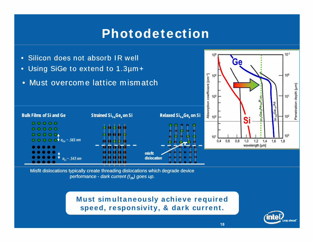
PhotodetectionPhotodetection
•• Silicon does not absorb IR wellSilicon does not absorb IR well•• Using SiGe to extend to 1.3µm+ Using SiGe to extend to 1.3µm+
GeGeGeGeGeGe
•• Must overcome lattice mismatchMust overcome lattice mismatch
SiSiSiSiBulk Films of Si and GeBulk Films of Si and Ge Strained SiStrained Si11--xxGeGex x on Sion Si Relaxed SiRelaxed Si11--xxGeGex x on Sion Si
aaGeGe ~ .565 nm~ .565 nm
aaSiSi ~ .543 nm~ .543 nmmisfitmisfitdislocationdislocation
Misfit dislocations typically create threading dislocations which degrade device Misfit dislocations typically create threading dislocations which degrade device performance performance -- dark current (Idark current (Idkdk) goes up) goes up..
M t i lt l hi i d
18
Must simultaneously achieve required speed, responsivity, & dark current.

Waveguide Photodetector DesignWaveguide Photodetector Design
PassivationPassivation
Rib waveguide
Passivation
P-contact
Si
N-contact
P-contact Ge
Rib waveguide
Passivation
P-contact
Si
N-contact
P-contact GeN-GeN-Ge
i-Geg
SiO2 (BOX)Si
Si (Substrate)
g
SiO2 (BOX)Si
Si (Substrate)
19
SEM Cross-Section

SiGe WG PIN SiGe WG PIN -- High Speed PerformanceHigh Speed Performance
3
(dB
) 7.4um x 50um, -2V4.4um x 100um, -2V
-3
0
35
Hz)po
nsiv
ity ( ,
-9
-6
10
15
20
25
30
7.4um x 50um 4.4um x 100um
Ban
dwid
th (
GH
ativ
e R
esp
40 Gb/s Eye Diagram
95% Quantum Efficiency108 109 1010
-120 1 2 3 4 5
5
Voltage (V)Rel
a
Frequency (Hz) 95% Quantum EfficiencyOperating at λ ~1.56um< 200nA of dark current
Frequency (Hz)
31 GHz Optical Bandwidth
20
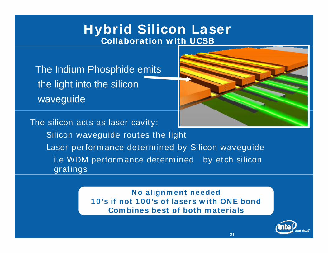
Hybrid Silicon LaserHybrid Silicon LaserCollaboration Collaboration with UCSBwith UCSB
The Indium Phosphide emits the light into the silicon waveguide
The silicon acts as laser cavity:Silicon waveguide routes the lightLaser performance determined by Silicon waveguide
i.e WDM performance determined by etch silicon gratings
No alignment needed10’s if not 100’s of lasers with ONE bond
21
Combines best of both materials

Hybrid Laser StructureHybrid Laser Structure
22
SEM (Scanning Electron Microscope) PhotographSEM (Scanning Electron Microscope) Photograph

Single Wavelength Hybrid LaserSingle Wavelength Hybrid LaserSingle Wavelength Hybrid LaserSingle Wavelength Hybrid Laser
Intel & UCSB integrateIntel & UCSB integrategggrating mirrors in silicon, grating mirrors in silicon, enabling wavelengthenabling wavelength--specificspecificlaser light outputlaser light output
~1000um~1000um
The DeviceThe Device
~150 ~150 umum
~1000um~1000um
IDF August 2008Inte Confidential

Single Wavelength ResultsSingle Wavelength Results
Optical SpectrumOptical Spectrum Linewidth MeasurementLinewidth Measurement
-- 8 8 mWmW output power at room temperatureoutput power at room temperature
Optical SpectrumOptical Spectrum Linewidth MeasurementLinewidth Measurement
8 8 mWmW output power at room temperatureoutput power at room temperature
-- Single wavelength with 50 dB side Single wavelength with 50 dB side mode suppression mode suppression ratioratio
-- 3.6 MHz line width (de3.6 MHz line width (de--convolved from measurement)convolved from measurement)
Inte Confidential

MotivationMotivationHistory & ProgressHistory & Progress
Intel’s Research ProgramIntel’s Research Program
Building Block ResultsBuilding Block Resultsgg––Modulator, detector, hybrid Modulator, detector, hybrid laserlaser
Integrated 200Gb/s Test chipIntegrated 200Gb/s Test chip
Future work & Summary Future work & Summary
25

Integrated SiP Test chipIntegrated SiP Test chipLearning Vehicle: target >100Gb/sLearning Vehicle: target >100Gb/s
Si MZMs 10-25Gb/sλ1
x x
1
λ2
1:8
Dem
ux
8:1
Muxinput output
λ1,λ2,…,λ8 λ1,λ2,…,λ8λ1,λ2,…,λ8
λ8
•• Learning vehicle forLearning vehicle for::P i iP i i
26
•• Process integration Process integration •• Electrical and high speed packagingElectrical and high speed packaging•• Performance, die variation, uniformity Performance, die variation, uniformity
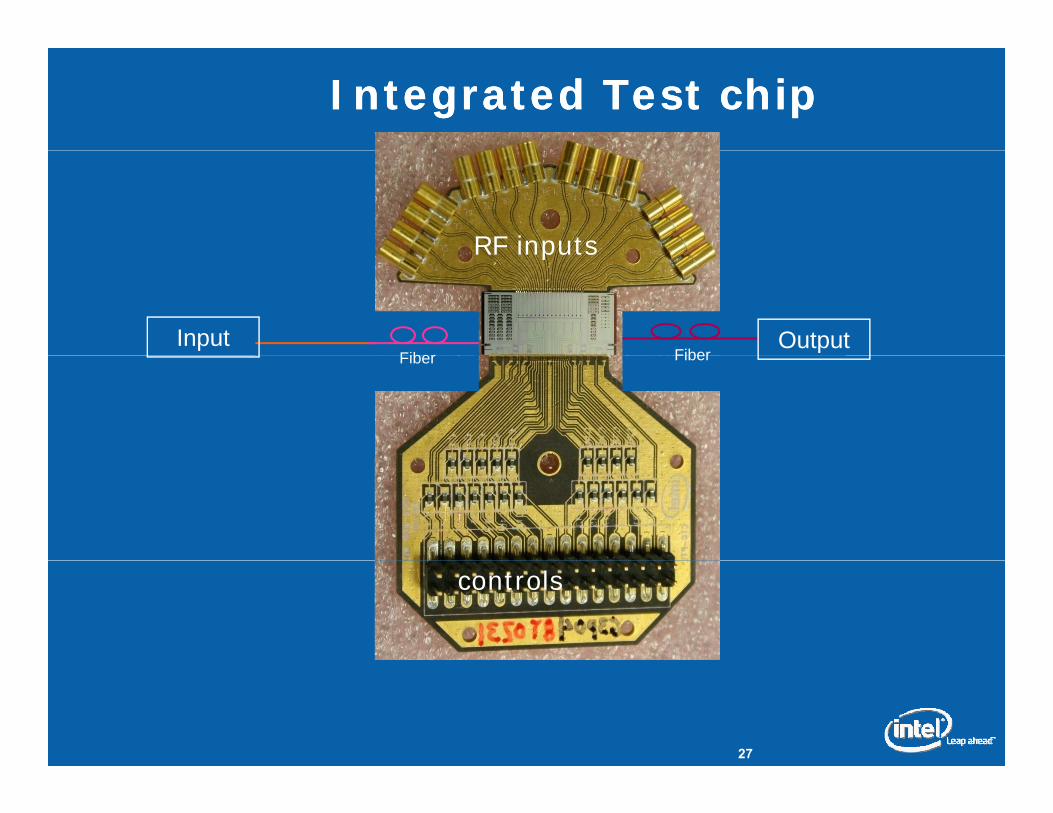
Integrated Test chipIntegrated Test chip
RF inputs
Fiber FiberOutput
RF inputs
InputFiber Fiber
controls
27
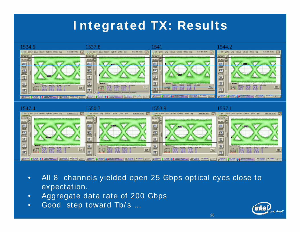
Integrated TX: ResultsIntegrated TX: Results
1534.6 1537.8 1541 1544.2
1547.4 1550.7 1553.9 1557.1
• All 8 channels yielded open 25 Gbps optical eyes close to expectation.
28
e pectat o• Aggregate data rate of 200 Gbps• Good step toward Tb/s …

Moti tionMoti tionMotivationMotivation
History & ProgressHistory & Progress
Intel’s Research ProgramIntel’s Research Program
Building Block ResultsBuilding Block Results
––Modulator, detector, hybrid Modulator, detector, hybrid laserlaser
Integrated 200Gb/s Test chipg / p
Future Future work & work & SummarySummaryFuture Future work & work & SummarySummary
29

Future: A Terabit Optical ChipFuture: A Terabit Optical Chip
Optical Fiber
Multiplexer
25 modulators at 40Gb/s
25 hybrid lasers25 hybrid lasers
A future integrated terabit per second i l li k i l hi
30
g poptical link on a single chip

Integrating into a TeraIntegrating into a Tera--scale Systemscale System
This transmitter This transmitter would be combined would be combined with a receiverwith a receiver
RxRx
TxTx
Which could then be built into an Which could then be built into an
31
Which could then be built into an Which could then be built into an integrated, silicon photonic chip!!integrated, silicon photonic chip!!

Integrating into a TeraIntegrating into a Tera--scale Systemscale System
This integrated silicon photonic This integrated silicon photonic hi ld th b i t t d hi ld th b i t t d chip could then be integrated chip could then be integrated
into computer boardsinto computer boards And this board could be And this board could be integrated into a Teraintegrated into a Tera--scascasystemsystem
32
yy

SummarySummaryFuture multiFuture multi--core processors will continue to drive I/O bandwidth core processors will continue to drive I/O bandwidth Future multiFuture multi--core processors will continue to drive I/O bandwidth core processors will continue to drive I/O bandwidth needs to ~Tb/s data rates in near future pushing need for optical needs to ~Tb/s data rates in near future pushing need for optical interconnectsinterconnects
Cost will be primary driver for enabling optical links in and around Cost will be primary driver for enabling optical links in and around the PC and Serverthe PC and Server
Silicon Photonics Silicon Photonics device performance advancing device performance advancing at a rapid rate. at a rapid rate. Need to continue pushing Need to continue pushing higher levels of integration (higher levels of integration (ieie 200G200G, , 400G etc) 400G etc) 400G etc) 400G etc)
Next phase of challenges will be with integration combined with Next phase of challenges will be with integration combined with l t k il t k ilow cost packaginglow cost packaging
Overall solution must focus on power efficiency, integration and Overall solution must focus on power efficiency, integration and cost tradeoffscost tradeoffs
33
cost tradeoffscost tradeoffs
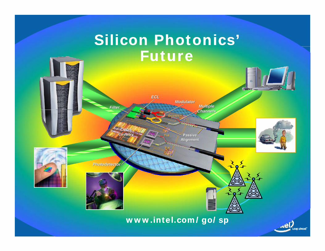
Silicon Photonics’Silicon Photonics’FutureFuture
ModulatorModulatorECLECL
FilterFilter MultipleMultipleCh lCh l
TIATIA
DriversDrivers
TIATIA
DriversDrivers
CMOSCMOSCircuitryCircuitry PassivePassive
AlignmentAlignment
ChannelsChannels
TIATIATIATIA
PhotodetectorPhotodetector
gg
34
www.intel.com/go/spwww.intel.com/go/sp

Electronics: Electronics: Economics of Moore’s LawEconomics of Moore’s Law
SCALING + WAFER SIZE + HIGH VOLUME = LOWER COST
35
Integration & increased functionality

The Opportunity of Silicon PhotonicsThe Opportunity of Silicon Photonics
Enormous ($ billions) CMOS infrastructure, process Enormous ($ billions) CMOS infrastructure, process
pp ypp y
($ ) , p($ ) , plearning, and capacity learning, and capacity –– Draft continued investmentDraft continued investment in Moore’s law in Moore’s law
Potential to integrate multiple optical devices Potential to integrate multiple optical devices Micromachining could provide smart packaging Micromachining could provide smart packaging Potential to converge computing & communicationsPotential to converge computing & communications
T b fit f thi ti l f
36
To benefit from this optical wafers must run alongside existing product.

Guiding Light with Si WaveguidesGuiding Light with Si Waveguides
Ex: Rib waveguide SEM IMAGES
Siliconoxide
Siliconoxide
Silicon
Proven area for siliconProven area for siliconHigh index High index == small structuressmall structures
St i d Ph t i t l f f th liSt i d Ph t i t l f f th li–– Strip and Photonic crystals for further scalingStrip and Photonic crystals for further scaling
Splitters, couplers, gratings, AWGs, MMIsSplitters, couplers, gratings, AWGs, MMIshave all been demonstratedhave all been demonstrated
37
Continue to reduce size while to reduce size while maintaining performancemaintaining performance