ignition coil driver power i.c. - farnell element14 · this is information on a product in full...
TRANSCRIPT

This is information on a product in full production.
March 2015 DocID024413 Rev 3 1/34
VBG08H-E
Ignition coil driver power I.C.
Datasheet - production data
Features
• Smart electronic ignition with embedded IGBT power stage
• Coil current limiter
• Current threshold flag diagnostic output
• Enable pin
• Slow turn-on
• Soft shut down (SSD) operated by low voltage clamp circuit (LVC)
• SSD activated by – Thermal intervention (Tj > 150°C)– Enable pin– Input overvoltage– Battery overvoltage
• Battery fault tolerant pins
• ESD protected
• TTL compatible
DescriptionVBG08H is a single channel driver, plus an IGBT power stage internally assembled using Chip On Chip (COC) hybrid technology.
The two chips are assembled together in the OctaPAK® package.
The device comes with several built-in protections like a coil current limiter, thermal monitoring circuit, which triggers a Soft Shut Down (SSD) as soon as the maximum allowable temperature is reached (TSD). It avoids extra voltage on the secondary side of the coil transformer.
The Slow Turn On circuit (STO), avoids unwanted sparks during first negative dV/dt of HVC voltage at turn on.
The current flag circuit provides an output logical signal voltage when the coil current reaches a fixed threshold.
HVCL INOM VS IS
360 V 8 A(1)
1. Max operative current
6 - 40 V 5 mA
Table 1. Device summary
PackageOrder codes
Tube Tape and reel
OctaPAK VBG08H-E VBG08HTR-E
www.st.com

Contents VBG08H-E
2/34 DocID024413 Rev 3
Contents
1 Detailed description . . . . . . . . . . . . . . . . . . . . . . . . . . . . . . . . . . . . . . . . . 5
1.1 Slow turn-on . . . . . . . . . . . . . . . . . . . . . . . . . . . . . . . . . . . . . . . . . . . . . . . . 6
1.2 Input over voltage (INP_OV) . . . . . . . . . . . . . . . . . . . . . . . . . . . . . . . . . . . 6
1.3 Battery overvoltage . . . . . . . . . . . . . . . . . . . . . . . . . . . . . . . . . . . . . . . . . . 6
2 Block diagram . . . . . . . . . . . . . . . . . . . . . . . . . . . . . . . . . . . . . . . . . . . . . . 7
3 Electrical specifications . . . . . . . . . . . . . . . . . . . . . . . . . . . . . . . . . . . . . . 9
3.1 Absolute maximum ratings . . . . . . . . . . . . . . . . . . . . . . . . . . . . . . . . . . . . 10
3.2 Thermal data . . . . . . . . . . . . . . . . . . . . . . . . . . . . . . . . . . . . . . . . . . . . . . .11
3.3 Electrical characteristics . . . . . . . . . . . . . . . . . . . . . . . . . . . . . . . . . . . . . . .11
4 Electrical transient requirements . . . . . . . . . . . . . . . . . . . . . . . . . . . . . 25
4.1 General setup . . . . . . . . . . . . . . . . . . . . . . . . . . . . . . . . . . . . . . . . . . . . . . 25
5 PCB layout suggestions and PGND disconnection . . . . . . . . . . . . . . . 27
6 Package and PCB thermal data . . . . . . . . . . . . . . . . . . . . . . . . . . . . . . . 28
6.1 OctaPAK thermal data . . . . . . . . . . . . . . . . . . . . . . . . . . . . . . . . . . . . . . . 28
7 Package informations . . . . . . . . . . . . . . . . . . . . . . . . . . . . . . . . . . . . . . . 31
7.1 ECOPACK® . . . . . . . . . . . . . . . . . . . . . . . . . . . . . . . . . . . . . . . . . . . . . . . 31
7.2 OctaPAK package information . . . . . . . . . . . . . . . . . . . . . . . . . . . . . . . . . 31
8 Revision history . . . . . . . . . . . . . . . . . . . . . . . . . . . . . . . . . . . . . . . . . . . 33
DocID024413 Rev 3 3/34
VBG08H-E List of tables
3
List of tables
Table 1. Device summary . . . . . . . . . . . . . . . . . . . . . . . . . . . . . . . . . . . . . . . . . . . . . . . . . . . . . . . . . . 1Table 2. Pin name and function . . . . . . . . . . . . . . . . . . . . . . . . . . . . . . . . . . . . . . . . . . . . . . . . . . . . . 8Table 3. Suggested component values for the application circuit. . . . . . . . . . . . . . . . . . . . . . . . . . . 10Table 4. Absolute maximum ratings . . . . . . . . . . . . . . . . . . . . . . . . . . . . . . . . . . . . . . . . . . . . . . . . . 10Table 5. Thermal data (estimated) . . . . . . . . . . . . . . . . . . . . . . . . . . . . . . . . . . . . . . . . . . . . . . . . . . 11Table 6. Power section . . . . . . . . . . . . . . . . . . . . . . . . . . . . . . . . . . . . . . . . . . . . . . . . . . . . . . . . . . . 11Table 7. Timing characteristics . . . . . . . . . . . . . . . . . . . . . . . . . . . . . . . . . . . . . . . . . . . . . . . . . . . . . 12Table 8. Electrical transient requirements (part 1/3) . . . . . . . . . . . . . . . . . . . . . . . . . . . . . . . . . . . . . 26Table 9. Electrical transient requirements (part 2/3) . . . . . . . . . . . . . . . . . . . . . . . . . . . . . . . . . . . . . 26Table 10. Electrical transient requirements (part 3/3) . . . . . . . . . . . . . . . . . . . . . . . . . . . . . . . . . . . . . 26Table 11. PCB properties . . . . . . . . . . . . . . . . . . . . . . . . . . . . . . . . . . . . . . . . . . . . . . . . . . . . . . . . . . 28Table 12. Thermal parameters . . . . . . . . . . . . . . . . . . . . . . . . . . . . . . . . . . . . . . . . . . . . . . . . . . . . . . 30Table 13. OctaPAK mechanical data . . . . . . . . . . . . . . . . . . . . . . . . . . . . . . . . . . . . . . . . . . . . . . . . . 32Table 14. Document revision history . . . . . . . . . . . . . . . . . . . . . . . . . . . . . . . . . . . . . . . . . . . . . . . . . 33

List of figures VBG08H-E
4/34 DocID024413 Rev 3
List of figures
Figure 1. Block diagram schematic . . . . . . . . . . . . . . . . . . . . . . . . . . . . . . . . . . . . . . . . . . . . . . . . . . . 7Figure 2. OctaPAK top view. . . . . . . . . . . . . . . . . . . . . . . . . . . . . . . . . . . . . . . . . . . . . . . . . . . . . . . . . 7Figure 3. Voltage and current conventions . . . . . . . . . . . . . . . . . . . . . . . . . . . . . . . . . . . . . . . . . . . . . 9Figure 4. Application circuit . . . . . . . . . . . . . . . . . . . . . . . . . . . . . . . . . . . . . . . . . . . . . . . . . . . . . . . . . 9Figure 5. Input control vs VHVC time definitions . . . . . . . . . . . . . . . . . . . . . . . . . . . . . . . . . . . . . . . . 13Figure 6. Electrical characteristics timing. . . . . . . . . . . . . . . . . . . . . . . . . . . . . . . . . . . . . . . . . . . . . . 14Figure 7. Current limit without TSD activation Tj < TSD . . . . . . . . . . . . . . . . . . . . . . . . . . . . . . . . . . 15Figure 8. Current limit followed by TSD activation (Tj = TSD) (case 1) . . . . . . . . . . . . . . . . . . . . . . . 16Figure 9. Current limit followed by TSD activation (Tj = TSD) (case 2) . . . . . . . . . . . . . . . . . . . . . . . 17Figure 10. Thermal cycling behavior . . . . . . . . . . . . . . . . . . . . . . . . . . . . . . . . . . . . . . . . . . . . . . . . . . 18Figure 11. Switch on attempt at Tj > TSSD . . . . . . . . . . . . . . . . . . . . . . . . . . . . . . . . . . . . . . . . . . . . . . 18Figure 12. Soft switch off caused by EN pin pulled high . . . . . . . . . . . . . . . . . . . . . . . . . . . . . . . . . . . 19Figure 13. Coil current discharge completion after releasing of EN pin . . . . . . . . . . . . . . . . . . . . . . . . 20Figure 14. Device behaviour when EN pin becomes high before low to high transition of Input
command . . . . . . . . . . . . . . . . . . . . . . . . . . . . . . . . . . . . . . . . . . . . . . . . . . . . . . . . . . . . . . 21Figure 15. Device behaviour when EN pin is pulled up and down while Input command is still high . 22Figure 16. Device behavior in case of Input over voltage . . . . . . . . . . . . . . . . . . . . . . . . . . . . . . . . . . 23Figure 17. Device behavior in case of battery over voltage . . . . . . . . . . . . . . . . . . . . . . . . . . . . . . . . . 23Figure 18. Current flag threshold vs temperature for IFLAG = 6.5 A . . . . . . . . . . . . . . . . . . . . . . . . . . . 24Figure 19. HV self clamped energy capability . . . . . . . . . . . . . . . . . . . . . . . . . . . . . . . . . . . . . . . . . . . 24Figure 20. General ISO Pulse schematic. . . . . . . . . . . . . . . . . . . . . . . . . . . . . . . . . . . . . . . . . . . . . . . 25Figure 21. ISO Pulse schematic for pulse type 5b. . . . . . . . . . . . . . . . . . . . . . . . . . . . . . . . . . . . . . . . 25Figure 22. OctaPAK on two-layers PCB . . . . . . . . . . . . . . . . . . . . . . . . . . . . . . . . . . . . . . . . . . . . . . . 28Figure 23. OctaPAK on four-layers PCB . . . . . . . . . . . . . . . . . . . . . . . . . . . . . . . . . . . . . . . . . . . . . . . 28Figure 24. Rthj-amb vs PCB copper area in open box free air condition (one channel on) . . . . . . . . . . 29Figure 25. OctaPAK thermal impedance junction ambient single pulse (one channel on) . . . . . . . . . 29Figure 26. Thermal fitting model of a double-channel HSD in OctaPAK . . . . . . . . . . . . . . . . . . . . . . . 30Figure 27. OctaPAK package dimensions . . . . . . . . . . . . . . . . . . . . . . . . . . . . . . . . . . . . . . . . . . . . . . 31

DocID024413 Rev 3 5/34
VBG08H-E Detailed description
33
1 Detailed description
VBG08H is a single channel driver, plus an IGBT power stage internally assembled using Chip On Chip (COC) hybrid technology. The Power Stage integrates the current shunt resistor for sensing the coil current, and the thermal diode for monitoring the temperature which triggers the TSD intervention.
The two chips are assembled together in the OctaPAK® package. The device is intended for driving huge inductive loads in harsh automotive environments (as electronic ignitions). The functional block diagram is shown in Figure 1.
The IGBT is controlled by the input signals pin INP. In particular, when the device is enabled (EN pin is at “0”), the transition low to high of INP pin turns-on the IGBT, while, the transition high to low of the same input signal, turns-off the IGBT causing an extra voltage on the secondary side of the coil transformer, generating a spark in the spark system plug.
The implemented features offer a specific design advantage that makes the VBG08H particularly suitable for E.C.U. applications.
The device comes with several built-in protections like a coil current limiter, a thermal monitoring circuit, which triggers a Soft Shut Down (SSD) as soon as the maximum allowable temperature is reached (TSD), avoiding to generate an extra voltage on the secondary side of the coil transformer.
Soft shut down is performed using a Low Voltage Clamp (LVC) circuit, which clamps the primary coil winding at a fixed voltage, with respect to the battery value: LVC is activated as the result of a logical OR combination among different fault conditions: thermal shutdown, input overvoltage, internal wire bonding disconnection, supply overvoltage, device disabling in ON-state (EN pin pulled high while INP pin is high).
All these fault events trigger the soft shut down operation and cause a slow discharge of the coil current, avoiding generating any undesired sparks.
If SSD is activated by TSD, the complete slow coil current discharge depends on the duration of input signal in the high state. If the input signal is high for a time longer than the coil discharge time, the SSD stays activated until the coil is completely discharged (zero coil current).
Anyway, if the input command signal arrives while the SSD is active, the LVC is immediately disabled for allowing the spark generation with the residual energy.
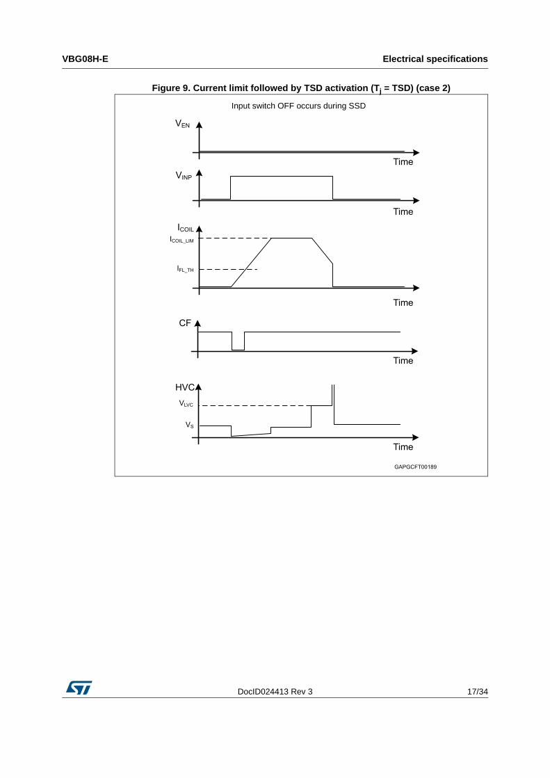
SSD timing diagrams are shown in Figure 7, Figure 8 and Figure 9.
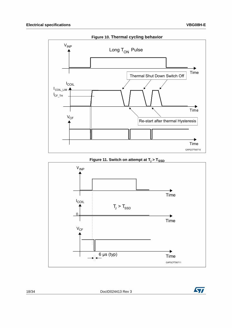
In case of thermal intervention, the IGBT remains switched off until the internal junction temperature, decreasing, reaches a lower temperature threshold, which corresponds to the fixed temperature hysteresis. In addition to the built-in protections above described, the chip is equipped with a single current flag diagnostic output.
Current Flag circuit provides an output logical signal voltage, which goes low (after a filtering time) when the input control pin goes high, and returns high when the coil current reaches a fixed value threshold. An internal voltage regulator, connected to the battery pin VS supplies all the internal circuitry.
The EN pin is intended as chip enable pin and it is used for enabling / disabling the device (see Figure 6).

Detailed description VBG08H-E
6/34 DocID024413 Rev 3
The event “EN pulled high” is stored inside internal register and causes the complete slow discharge of coil current.
Device can restart when the EN pin is pulled low and after the first low to high transition of the input pin. Figure 12, Figure 13, Figure 14 and Figure 15, show device behavior, with different combinations of INP and EN signal pins. This pin is provided with an internal pull-up current source, which disables the chip by default, in case the pin is left floating.
1.1 Slow turn-onDevice is internally equipped with a completely integrated Slow Turn On circuit (STO), that helps avoiding unwanted sparks during first negative dV/dt of HVC voltage at turn on (see Figure 5).
1.2 Input over voltage (INP_OV)Device is internally equipped with a built in protection which is activated in case of command input pin over voltage. If the input pin is shorted with a supply voltage (VBATT or VS), which is above the internal fixed threshold “INP_OV_TH_H”, the device operates a soft shutdown which slowly discharges the coil current. This event is managed by the device as a “real time event”, so the completion of coil current discharge depends on the time duration of the INP_OV detection. As soon as the INP_OV condition is removed (voltage at input pin decreases below the second lower threshold voltage “INP_OV_TH_H - INP_OV_HYS”), the device can be switched on, if a normal high state voltage is applied on the command input pin. See Figure 16 for more details.
1.3 Battery overvoltageWhen the supply voltage VS overcomes the "VS_OFF_TH" (battery load dump) for a time longer than 220 µs (typ), the device operates a soft shutdown until the complete coil current discharge. The device remains switched off until the battery voltage falls under the second lower threshold voltage, which corresponds to the prefixed hysteresis parameter “VS_OFF_HYS”.
Once this condition is verified, only a low to high transition of command input pin can turn on the device. See Figure 17 for more details.

DocID024413 Rev 3 7/34
VBG08H-E Block diagram
33
2 Block diagram
Figure 1. Block diagram schematic
Figure 2. OctaPAK top view

Block diagram VBG08H-E
8/34 DocID024413 Rev 3
Table 2. Pin name and function
Pin number Pin name Pin function
1 PGND1 Power GND
2 INP Input control pin / pulled down if left floating
3 VS Battery supply voltage
4 EN Chip enable control pin / pulled up if left floating
5 GND Controller GND
6 C.F. Current flag output / open drain
7 PGND2 Power GND
TAB HVC IGBT HV collector

DocID024413 Rev 3 9/34
VBG08H-E Electrical specifications
33
3 Electrical specifications
Figure 3. Voltage and current conventions
Figure 4. Application circuit

Electrical specifications VBG08H-E
10/34 DocID024413 Rev 3
3.1 Absolute maximum ratingsStressing the device above the ratings listed in Table 4 may cause permanent damage to the device itself. These are stress ratings only and operation of the device at these or any other conditions above those indicated in the operating sections of this specification is not implied. Exposure to the conditions reported in this section for extended periods may affect device reliability.
Table 3. Suggested component values for the application circuit
Type Description Value
R1 CFlag filter resistor 1 K
R2 CFlag filter resistor ≥ 4 K
C1 VCC capacitor 100 nF
C2 VCC capacitor 10 µF
C3 CFlag filter capacitor (1)
1. Application dependent.
Table 4. Absolute maximum ratings(1)
1. Refer to Figure 3 for voltage or currents conventions.
Symbol Parameter Value Unit
VHVC Collector voltage (internally limited) -16 to Vclamp V
IHVC Collector current (internally limited) Internally limited A
VS I.C. supply voltage range -0.3 to 40 V
VINP Input voltage -0.3 to 28 V
VCF Current flag output voltage -0.3 to 5.5 V
ICF Flag output current 1.5 mA
VEN Enable voltage -0.3 to 28 V
ESCIS25 Single pulse SCIS energy (Tj = 25°C; L = 6 mH) 265 mJ
ESCIS150 Single pulse SCIS energy (Tj = 150°C; L = 6 mH) 175(2)
2. In case of the device switch-off occurs in current limitation with open secondary condition, the energy limit must not be exceeded. The double fault condition is not provided.
mJ
VESD ESD voltage (HVC pin) (HBM: R = 1.5 KΩ; C = 100 pF) 4 KV
VESD ESD voltage (all pins) (HBM: R = 1.5 KΩ; C = 100 pF) 2 KV
Tj Operating junction temperature -40 to 175 °C
Tstg Storage temperature range -55 to 175 °C
I(HVC)_UNDGND Max underground collector current (t_app ≤ 100 µs) -6 A
tSC_MAX
Short circuit withstand time RSC = 0 Ω; IHVC = 10.5 A (maximum current limitation)– VS up to 16 V
– 16 V < VS ≤ 24 V– 24 < VS ≤ 28V
No constrains
52
msms

DocID024413 Rev 3 11/34
VBG08H-E Electrical specifications
33
3.2 Thermal data
3.3 Electrical characteristics-40°C < Tj < 150°C; VS = 6 ÷ 28 V, unless otherwise specified.
6:
Table 5. Thermal data (estimated)
Symbol Parameter Value Unit
Rtj-case Thermal resistance junction-case 0.55 °C/W
Rtj-amb Thermal resistance junction-ambient see Figure 24 °C/W
Table 6. Power section
Symbol Parameter Test condition Min. Typ. Max. Unit
VHV_CLAMP VHVC high voltage clamp IHVC = 6.5 A 320 360 400 V
VLV_CLAMP VHVC low voltage clamp IHVC = 6.5 A VS + 7 VS + 10 VS + 13 V
VCE_SAT1VHVC: collector to emitter saturation voltage
VS = 13.5 V; IHVC = 4 A 1.5 V
VCE_SAT2VHVC: collector to emitter saturation voltage
VS = 13.5 V; IHVC = 6.5 A
1.8 V
IS_STBY Standby supply currentIN = 0; EN = 0; IN = X; EN = 1; VS = 13.5 V
5 6 mA
VSOperative DC supply voltage
5.4 28 V
VS_OFF_TH VS overvoltage threshold 29 32 35 V
VS_OFF_HYS VS overvoltage hysteresis
0.5 3 V
ICOIL_NOMOperative coil current range
0 8 A
ICOIL_LIM Coil current limit
-40°C < Tj < 125°C; VS = 6 V
10.5 A
-40°C < Tj < 125°C; 9 V ≤ VS ≤ 28 V
8.5 9.5 10.5 A
ICES
Collector current (including the RHV contribution)
VCE = 28 V; VINP = 0 V; Tj = 125°C
0.3 1 mA
VINP_H High level input voltage 3 V
VINP_L Low level input voltage 1.5 V
VINP_HYSInput threshold hysteresis
0.2 V
IIN_PDW Input pull down current VINP = 4 V 10 20 30 µA
INP_OV_TH_HInput overvoltage activation threshold
8 9 10 V

Electrical specifications VBG08H-E
12/34 DocID024413 Rev 3
INP_OV_HYSInput overvoltage hysteresis
0.8 1.4 2 V
VCF_LLow level C.F. output voltage
ICF = 1 mA 0.8 V
ICF_leakageLeakage current on flag output
VINP = 0; VCF = 4 V; VS = 13.5 V
10 µA
ICF_TH_6.5Coil current level threshold 6.5 A(1)
-40°C ≤ Tj < 25°C 5.85 7
A25°C ≤ Tj < 100°C 6 6.85
100°C ≤ Tj < 125°C 6.2 6.8
125°C ≤ Tj ≤ 150°C 6.05 6.95
TSSDThermal shutdown intervention
150 175 °C
TSSD_HYS Thermal hysteresis 17 25 33 °C
VEN_HHigh level enable voltage
3 V
VEN_L Low level enable voltage VOUT free to follow VINP 1.5 V
VEN_HYS EN input hysteresis 0.2 V
-IEN_PUEnable pin pull up current
VEN = 0 V 10 20 30 µA
1. See Figure 18: Current flag threshold vs temperature for IFLAG = 6.5 A).
Table 7. Timing characteristics
Symbol Parameter Test condition Min. Typ. Max. Unit
fCLK 1.5 2 2.5 MHz
tFT_CF Current flag filtering time 16/fCLK µs
tFT_EN Enable filtering time 32/fCLK µs
tFT_INP Input filtering time 32/fCLK µs
tdON
Delay time from INP rising edge to VHVC = 0.9 VS (see Figure 5)
EN = 0; Tj = 25°C 30(1)
1. Including tFT_INP.
µs
(ΔVHVC/Δt)ONHVC slope during turn-on (see Figure 5)
EN = 0; Tj = 25°C; VS = 13.5 V
0.1 0.3 1 V/µs
tdOFF
Delay time from INP falling edge to VHVC = 100 V (see Figure 5)
ICOIL = 6.5 A; EN = 0; Tj = 25°C
25 µs
HVC3V STO deactivation threshold Tj = 25°C; VS = 13.5 V 3 5 V
Table 6. Power section (continued)
Symbol Parameter Test condition Min. Typ. Max. Unit

DocID024413 Rev 3 13/34
VBG08H-E Electrical specifications
33
Figure 5. Input control vs VHVC time definitions

Electrical specifications VBG08H-E
14/34 DocID024413 Rev 3
Figure 6. Electrical characteristics timing

DocID024413 Rev 3 15/34
VBG08H-E Electrical specifications
33
Figure 7. Current limit without TSD activation Tj < TSD

Electrical specifications VBG08H-E
16/34 DocID024413 Rev 3
Figure 8. Current limit followed by TSD activation (Tj = TSD) (case 1)
Input Switch OFF occurs after SSD completion
DocID024413 Rev 3 17/34
VBG08H-E Electrical specifications
33
Figure 9. Current limit followed by TSD activation (Tj = TSD) (case 2)
Input switch OFF occurs during SSD
Electrical specifications VBG08H-E
18/34 DocID024413 Rev 3
Figure 10. Thermal cycling behavior
Figure 11. Switch on attempt at Tj > TSSD

DocID024413 Rev 3 19/34
VBG08H-E Electrical specifications
33
Figure 12. Soft switch off caused by EN pin pulled high

Electrical specifications VBG08H-E
20/34 DocID024413 Rev 3
Figure 13. Coil current discharge completion after releasing of EN pin

DocID024413 Rev 3 21/34
VBG08H-E Electrical specifications
33
Figure 14. Device behaviour when EN pin becomes high before low to high transition of Input command

Electrical specifications VBG08H-E
22/34 DocID024413 Rev 3
Figure 15. Device behaviour when EN pin is pulled up and down while Input command is still high

DocID024413 Rev 3 23/34
VBG08H-E Electrical specifications
33
Figure 16. Device behavior in case of Input over voltage
Figure 17. Device behavior in case of battery over voltage

Electrical specifications VBG08H-E
24/34 DocID024413 Rev 3
Figure 18. Current flag threshold vs temperature for IFLAG = 6.5 A
Figure 19. HV self clamped energy capability

DocID024413 Rev 3 25/34
VBG08H-E Electrical transient requirements
33
4 Electrical transient requirements
4.1 General setupAll ISO pulses are performed according to the following schematics (see Figure 20 and Figure 21).
All ground pins (PGND1, GND and PGND2) are connected together as short as possible on the test board. The other pins (INP, EN, CF) are left open.
The load resistor is a nominal resistor 2 Ω. For breakdown level, for ISO1 and 2a 10 pulses are applied, and for ISO3a and 3b, test is applied during 1 minute.
Figure 20. General ISO Pulse schematic
Figure 21. ISO Pulse schematic for pulse type 5b

Electrical transient requirements VBG08H-E
26/34 DocID024413 Rev 3
Table 8. Electrical transient requirements (part 1/3)
ISO 7637-2 2004 (E)
Test Pulse
Test level Number of pulse or
test times
Burst cycle / pulse repetition time
Delay and impedanceIII IV
1 -75 -100 5000 pulses 0.5 s 5 s 2 ms, 10 Ω
2a +37 +50 5000 pulses 0.2 s 5 s 50 µs, 2 Ω
3a -100 V -150 V 1 h 90 ms 100 ms 0.1 µs, 50 Ω
3b +75 V +100 V 1 h 90 ms 100 ms 50 µs, 2 Ω
4 -6 V -7 V 1 pulse 100 ms, 0.01 Ω
5b(1)
1. External load dump clamp, 40 V max, refereed to ground.
65 8 V 1 pulse 100 ms, 0.01 Ω
Table 9. Electrical transient requirements (part 2/3)
ISO 7637-2 2004 (E)
Test Pulse
Test level
III IV
1 C C
2a C C
3a C C
3b C C
4 C C
5b(1)
1. External load dump clamp, 40V max, refereed to ground.
C C
Table 10. Electrical transient requirements (part 3/3)
Class Content
C All function of the device is performed as designed after exposure to disturbance
EOne or more functions of the device are not performed as designed after exposure to disturbance and cannot be returned to proper operation without replacing the device.

DocID024413 Rev 3 27/34
VBG08H-E PCB layout suggestions and PGND disconnection
33
5 PCB layout suggestions and PGND disconnection
Device is provided with two power gnd leads perfectly symmetrical. Therefore, the current flowing trough each lead is exactly half of the one flowing trough coil and IGBT power stage collector. PCB power GNDs tracks must be as much symmetrical as possible respect to the Power GND node, in order to always maintain IPGND1 = IPGND2 (see Figure 4).
A difference voltage V, between PGND1 an PGND2 causes a misalignment between ICOIL_LIM and ICF_TH.
In case of only PGND2 disconnection the device is still operative, but its coil current is limited till a maximum value of ½ ICOIL_LIM. Current Flag signal operates, but its threshold value is also reduced at ½ ICF_TH.
If, instead, only PGND1 is disconnected from the power GND, the coil current is controlled only by the width of input command signal (no limitation). Furthermore, the C.F. signal is kept in the low state for all duration of Input command signal.

Package and PCB thermal data VBG08H-E
28/34 DocID024413 Rev 3
6 Package and PCB thermal data
6.1 OctaPAK thermal data
Figure 22. OctaPAK on two-layers PCB
Figure 23. OctaPAK on four-layers PCB
Table 11. PCB properties
Dimension Value
Board finish thickness 1.6 mm +/- 10%
Board dimension 78 mm x 86 mm
Board Material FR4
Copper thickness (top and bottom layers) 0.070 mm
Copper thickness (inner layers) 0.035 mm
Thermal vias separation 1.2 mm
Thermal via diameter 0.3 mm +/- 0.08 mm
Copper thickness on vias 0.025 mm
Footprint dimension 6.4 mm x 7mm

DocID024413 Rev 3 29/34
VBG08H-E Package and PCB thermal data
33
Figure 24. Rthj-amb vs PCB copper area in open box free air condition (one channel on)
Figure 25. OctaPAK thermal impedance junction ambient single pulse (one channel on)
Equation 1: pulse calculation formula
where δ = tP/T
ZTHδ RTH δ ZTHtp 1 δ–( )+⋅=
Package and PCB thermal data VBG08H-E
30/34 DocID024413 Rev 3
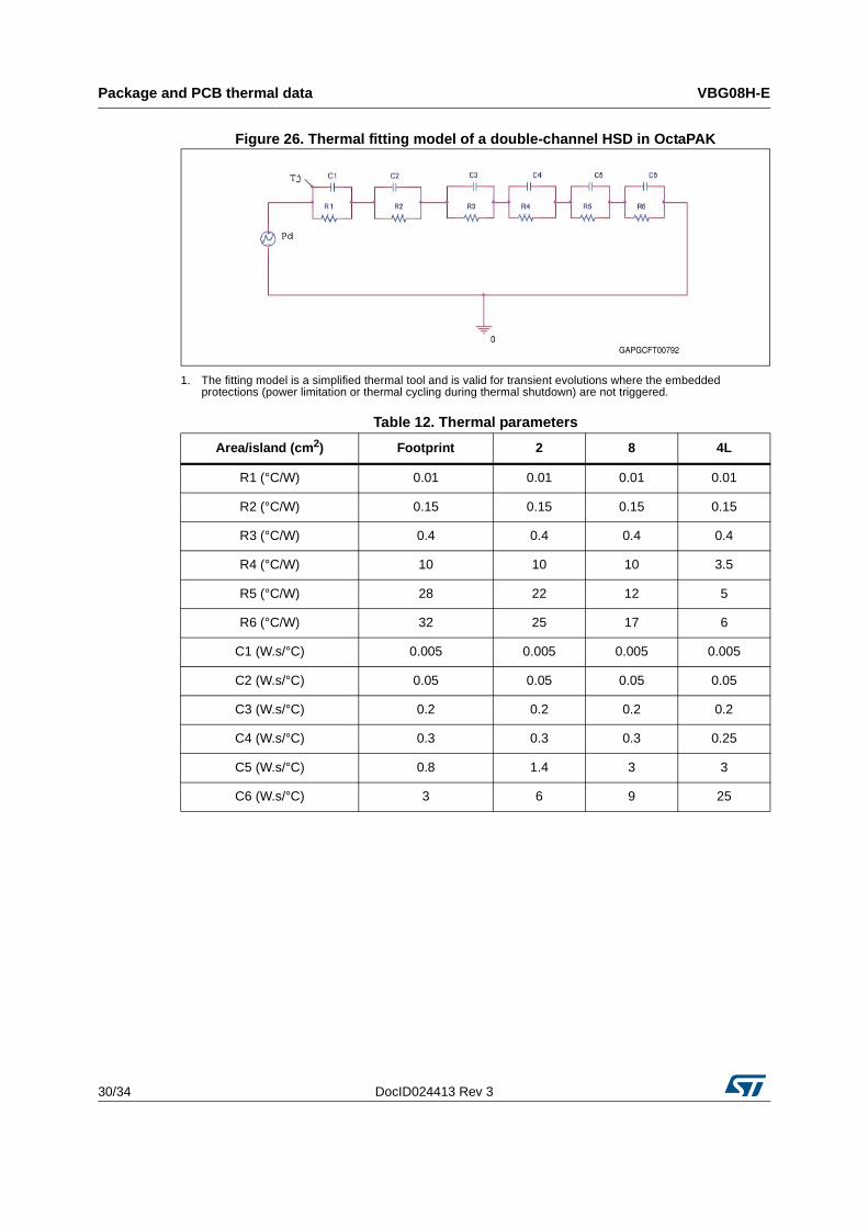
Figure 26. Thermal fitting model of a double-channel HSD in OctaPAK
1. The fitting model is a simplified thermal tool and is valid for transient evolutions where the embedded protections (power limitation or thermal cycling during thermal shutdown) are not triggered.
Table 12. Thermal parameters
Area/island (cm2) Footprint 2 8 4L
R1 (°C/W) 0.01 0.01 0.01 0.01
R2 (°C/W) 0.15 0.15 0.15 0.15
R3 (°C/W) 0.4 0.4 0.4 0.4
R4 (°C/W) 10 10 10 3.5
R5 (°C/W) 28 22 12 5
R6 (°C/W) 32 25 17 6
C1 (W.s/°C) 0.005 0.005 0.005 0.005
C2 (W.s/°C) 0.05 0.05 0.05 0.05
C3 (W.s/°C) 0.2 0.2 0.2 0.2
C4 (W.s/°C) 0.3 0.3 0.3 0.25
C5 (W.s/°C) 0.8 1.4 3 3
C6 (W.s/°C) 3 6 9 25
DocID024413 Rev 3 31/34
VBG08H-E Package informations
33
7 Package informations
7.1 ECOPACK®
In order to meet environmental requirements, ST offers these devices in different grades of ECOPACK® packages, depending on their level of environmental compliance. ECOPACK® specifications, grade definitions and product status are available at: www.st.com. ECOPACK® is an ST trademark.
7.2 OctaPAK package information
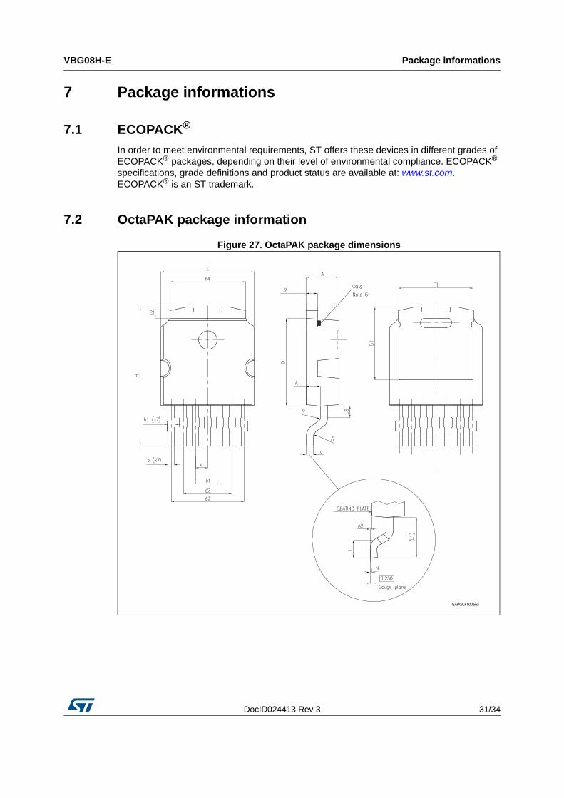
Figure 27. OctaPAK package dimensions

Package informations VBG08H-E
32/34 DocID024413 Rev 3
Table 13. OctaPAK mechanical data
SymbolMillimeters
Min. Typ. Max.
A 2.20 2.30 2.40
A1 0.90 1.00 1.10
A2 0.03 0.10 0.23
b 0.45 0.52 0.60
b1 0.70
b4 5.20 5.30 5.40
c 0.45 0.50 0.60
c2 0.75 0.80 0.90
D 6.00 6.10 6.20
D1 5.15
E 6.40 6.50 6.60
E1 5.30
e 0.85
e1 1.60 1.70 1.80
e2 3.30 3.40 3.50
e3 5.00 5.10 5.20
H 9.35 9.70 10.10
L 1.00 —
(L1) 2.80
L2 0.80
L3 0.85
R 0.40 0.65
V2 0° 8°

DocID024413 Rev 3 33/34
VBG08H-E Revision history
33
8 Revision history
Table 14. Document revision history
Date Revision Changes
28-Mar-2013 1 Initial release
16-Sep-2013 2 Updated disclaimer
26-Mar-2015 3Table 7: Timing characteristics:
– tdOFF: updated test condition and value
VBG08H-E
34/34 DocID024413 Rev 3
IMPORTANT NOTICE – PLEASE READ CAREFULLY
STMicroelectronics NV and its subsidiaries (“ST”) reserve the right to make changes, corrections, enhancements, modifications, and improvements to ST products and/or to this document at any time without notice. Purchasers should obtain the latest relevant information on ST products before placing orders. ST products are sold pursuant to ST’s terms and conditions of sale in place at the time of order acknowledgement.
Purchasers are solely responsible for the choice, selection, and use of ST products and ST assumes no liability for application assistance or the design of Purchasers’ products.
No license, express or implied, to any intellectual property right is granted by ST herein.
Resale of ST products with provisions different from the information set forth herein shall void any warranty granted by ST for such product.
ST and the ST logo are trademarks of ST. All other product or service names are the property of their respective owners.
Information in this document supersedes and replaces information previously supplied in any prior versions of this document.
© 2015 STMicroelectronics – All rights reserved