iii-nitrides - arxiv.org · the i direction and e3i are the corresponding piezoelec-tric constants...
TRANSCRIPT

arX
iv:1
605.
0762
9v1
[co
nd-m
at.m
trl-
sci]
24
May
201
6
Correct implementation of polarization constants in wurtzite materials and impact on
III-nitrides
Cyrus E. Dreyer,1, 2 Anderson Janotti,1, ∗ Chris G. Van de Walle,1 and David Vanderbilt2
1Materials Department, University of California, Santa Barbara, CA 93106-50502Department of Physics and Astronomy, Rutgers University, Piscataway, NJ 08845-0849
(Dated: May 26, 2016)
Accurate values for polarization discontinuities between pyroelectric materials are critical forunderstanding and designing the electronic properties of heterostructures. For wurtzite materials,the zincblende structure has been used in the literature as a reference to determine the effectivespontaneous polarization constants. We show that, because the zincblende structure has a nonzeroformal polarization, this method results in a spurious contribution to the spontaneous polarizationdifferences between materials. In addition, we address the correct choice of “improper” versus“proper” piezoelectric constants. For the technologically important III-nitride materials GaN, AlN,and InN, we determine polarization discontinuities using a consistent reference based on the layeredhexagonal structure and the correct choice of piezoelectric constants, and discuss the results in lightof available experimental data.
PACS numbers: 77.22.Ej,73.40.Lq,85.60.Bt
I. INTRODUCTION
Pyroelectric materials have emerged in a variety ofelectronic and optoelectronic applications. Because ofthe symmetry of their crystal structure these materialsexhibit spontaneous (SP) and piezoelectric (PZ) dipolemoments [1] which manifest themselves as electric fieldsin heterostructure layers and sheet charges at interfaces.In the technologically important III-nitrides, which havethe wurtzite (WZ) structure (space group P63mc), po-larization differences allow for strong carrier confine-ment and the formation of a two-dimensional electrongas (2DEG) with high density at AlGaN/GaN interfaces,exploited in high electron mobility transistors (HEMTs).The effect of polarization can also be detrimental, forexample causing the quantum-confined Stark effect inquantum wells of light-emitting diodes (LEDs), which re-duces radiative recombination rates and shifts the emis-sion wavelength. For both HEMTs and LEDs, accuratevalues of the SP and PZ polarization constants are re-quired for a fundamental understanding as well as fordevice design.Since experimental determination of the separate SP
and PZ contributions to the total polarization is verydifficult, calculated values of SP and PZ polarization con-stants are widely used in simulations. The PZ polariza-tion constants are, in principle, fairly straightforward toexplicitly measure or calculate [2]. However, the reportedvalues exhibit a considerable spread [3]. In addition, thedifference between so-called “proper” and “improper” PZconstants [2, 4] is often overlooked, even though it cangive rise to significant quantitative changes in the result-ing polarization fields. This difference is one issue thatis elucidated in the present paper.
∗ Current address: Materials Science and Engineering, University
of Delaware, Newark, Delaware 19716-1501, USA
The definition of SP polarization constants is evenmore subtle, and they are typically not amenable to ex-plicit experimental determination, except in special cases[5]. The calculation of SP polarization requires the choiceof a reference structure, which in the case of WZ semi-conductors, has invariably been chosen to be zincblende(ZB) [6–8]. In this work we will show that though ZB asa reference structure is intuitively appealing, the SP po-larization constants that result have been misinterpreted,introducing a source of error into the predicted values forbound sheet charge densities (and polarization fields).We also demonstrate that a proper choice of referencestructure can eliminate these problems, and we providerevised values that can be directly inserted in currentsimulation tools.While our theoretical considerations are general, we
choose the nitride semiconductors because they providea suitable example to illustrate the derivations, and be-cause our findings have a significant impact on this ma-terials system of high (and still increasing) technologicalimportance. In Sec. II we review the underlying the-ory. In Sec. III we address the problems with choos-ing zincblende as a reference structure, and propose asolution. Sec. IV deals with piezoelectric contributions,specifically the issue of proper versus improper constants.In Sec. V we show that our findings have important con-sequences for nitride device structures and compare withprevious implementations and with experiment. Sec-tion VI concludes the paper.
II. CALCULATING POLARIZATIONCONSTANTS IN WURTZITE
For WZ films grown in the [0001] direction (i.e., the+c direction), the polarization component P3 is given bythe sum of the SP polarization at the wurtzite material’sown lattice parameters, PSP, and the z component of the

2
PZ polarization [1]. That is, for material m,
Pm3 = Pm
SP + (ǫm1 + ǫm2 )em31 + ǫm3 em33, (1)
where (in Voigt notation) ǫi (i=1,2,3) is the strain inthe i direction and e3i are the corresponding piezoelec-tric constants (specifically, the “improper” ones; see Sec-tion IV). Henceforth we drop the subscript “3” from P forsimplicity; all unbolded quantities pertaining to wurtziteare assumed to be in the c direction.The goal of this work is to derive the appropriate SP
and PZ constants that allow Eq. (1) to be used in accu-rately determining polarization differences at interfacesbetween different WZ materials.
A. The modern theory of polarization
Direct calculation of the polarization constants inEq. (1) by first-principles electronic-structure methodswas enabled by the formulation of a rigorous theory ofbulk polarization, known as the modern theory of polar-ization (MTP) [9, 10]. For a given structure λ, the MTPallows calculation of the so-called “formal” polarization[9]:
Pf = Pion +Pel
=e
Ω
∑
s
Z ions R
(λ)s +
ief
8π3
occ∑
j
∫
BZ
dk〈u(λ)j,k |∇k|u(λ)
j,k〉,
(2)
where Ω is the cell volume, Z ions is the charge of the
ion s and R(λ)s is its position in the λ structure, f is
the spin degeneracy of the bands, the sum j runs over
occupied bands, and u(λ)j,k are the cell periodic parts of
the Bloch wave functions. In Eq. (2), Pel is the Berryphase taken over the valence-band manifold [9, 10]. Theformal polarization is defined only modulo the “quantumof polarization” eR/Ω, where R is any lattice constantand e is the electron charge [9, 10].In the MTP, only differences between formal polariza-
tions of appropriate structures, λ = 0 and λ = 1, are welldefined:
∆P = P(λ=1)f −P
(λ=0)f . (3)
The choice of the “appropriate” structures λ = 0 and λ =1 rests on one of two possible considerations to ensurethat physical conclusions can be drawn from their formalpolarization differences. First, if the two structures areconnected by an adiabatic, gap-preserving deformationpath [9, 10], then their difference in polarization [∆P inEq. (3)] is given by the expression
∆P =
∫ 1
0
dλ∂P
∂λ, (4)
and corresponds to the zero-field adiabatic displacementcurrent. This quantity can, in principle, be determined
experimentally. An obvious application is the calculationof piezoelectric constants, which involves polarization dif-ferences between structures with slightly different latticeconstants and/or internal structural parameters.
B. Interface theorem
The second consideration, as shown by Vanderbilt andKing-Smith [11], is that if an insulating interface can beconstructed between two structures, the difference in for-mal polarization gives the bound charge, σb, that buildsup at the interface as a result of the continuity of thedisplacement field over an interface with no free charge:
σb = (Pλ=1f −P
λ=0f ) · n. (5)
This is often referred to as the “interface theorem.” Sincethere is no adiabatic path necessary between the twostructures in this consideration, λ = 0 and λ = 1 canbe different polymorphs of the same material (such asWZ and ZB structures of GaN) or different materials al-together (such as GaN and AlN); as long as they form aninsulating interface, Eq. (5) will give the bound chargeaccumulation at the interface.From the interface theorem [Eq. (5)] and Eq. (1), the
bound polarization charge at the interface between dif-ferent III-nitride materials (m and n) is
σb = [PmSP + em31(ǫ
m1 + ǫm2 ) + em33ǫ
m3 ]
− [PnSP + en31(ǫ
n1 + ǫn2 ) + en33ǫ
n3 ] .
(6)
As an example, we will take a realistic situation thatoccurs in heterostructures, by assuming that material nis strained coherently to m (ǫm1 = ǫm2 = ǫm3 = 0), i.e.,under plane stress (ǫn1 = ǫn2 , ǫ
n3 = −2Cn
13/Cn33ǫ
n1 , where
Cij are the elastic constants). Therefore we have
σb = (PmSP − Pn
SP)− 2ǫn1 (en31 − en33C
n13/C
n33)
= ∆P intSP − 2ǫn1 (e
n31 − en33C
n13/C
n33).
(7)
Note that σb is the charge density of electrons at an in-terface for which material n has been grown on top ofmaterial m in the +c direction.
III. REFERENCE STRUCTURE FORSPONTANEOUS POLARIZATION
A. Effective spontaneous polarization constants
We will first address the difference in spontaneous po-larization in Eq. (7), ∆P int
SP . Strain effects will be takeninto account separately in the PZ part, so that ∆P int
SP issimply the difference of formal polarizations of the re-spective zero-strain structures,
∆P intSP = Pm
f
∣∣ǫ=0
− Pnf
∣∣ǫ=0
. (8)

3
For purposes of Eq. (1), we would like to define a SPpolarization constant that is a property of a single mate-rial. Simply taking Pm
f of Eq. (8) as PmSP is problematic,
since formal polarization is multivalued, being only well-defined modulo a quantum of polarization eR/Ω. There-fore, in every situation in which Eq. (1) is applied todetermine σb at an interface, it must be confirmed thatformal polarizations of the two materials are taken onthe same “branch” of eR/Ω. A better approach is totake Pm
SP in Eq. (1) as a so-called “effective” SP polar-ization, Peff, defined by Resta and Vanderbilt [12] to bethe ∆P in Eq. (3) that results as the system is takenfrom a high-symmetry “reference” structure (λ = 0) tothe structure of interest (λ = 1). That is,
Peff = P(λ=1)f −P
(λ=0)f = Pf −P
reff . (9)
Using Peff to define the SP polarization of the materialremoves the indeterminacy inherent to the formal polar-ization.The reference structure is often chosen to be cen-
trosymmetric, but it is important to recognize that theformal polarization of centrosymmetric crystals is notnecessarily zero. This is because, as stated above, Pf isa multivalued vector field, so it is possible for a nonzeroformal polarization to be unchanged (modulo eR/Ω) un-der the inversion operator. Nevertheless, high symmetry
puts restrictions on the possible values of P(λ=0)f [11].
While in principle effective polarization constants arestill differences in formal polarization between λ = 1 andλ = 0 (reference) structures, in practice they can be usedto compare spontaneous polarizations of different mate-rials to obtain ∆PSP if such materials share a referencestructure with the same formal polarization. Such a com-parison then correctly yields the interface charge densityaccording to the interface theorem of Ref. 11. In suchcases, ∆PSP is just given by the difference in effective SPpolarization of the materials,
∆P intSP = Pm
eff − Pneff. (10)
In the more general case that the reference formal po-larizations do not match, the correct change in SP polar-ization following from Eqs. (8) and (9) is
∆P intSP = ∆P int
SP + (Pm,reff − Pn,ref
f ). (11)
That is, a correction term of the form
∆P refcorr ≡ Pm,ref
f − Pn,reff (12)
has to be added to Eq. (10). Unfortunately, this correc-tion term is not typically implemented in device simula-tion packages (e.g., Ref. 13) or used in the interpretationof experimental data (e.g., Ref. 14, which is considered astandard reference in the field).When the PZ terms are included as well, the total in-
terface charge given by Eq. (7) becomes
σb = ∆P intSP +∆P ref
corr − 2ǫn1 (en31 − en33C
n13/C
n33). (13)
Equation (13) is a central result of the present work.
B. Correction term for the effective spontaneouspolarization with the zincblende reference structure
As mentioned before, previous studies [6–8] have exclu-sively used ZB (space group F 43m) as a reference struc-ture for calculating the SP polarization of the WZ. Thisstructure is not centrosymmetric, although it has suffi-cient symmetry to preclude any SP polarization [1]. Thefact that an insulating (111) interface can be constructedbetween the WZ and ZB polytypes [8] makes it an ap-propriate reference structure. In fact, experimental mea-surements have deduced the relative polarization betweenthe WZ and ZB phases of GaN [5], which were found tobe consistent with the theoretical values in Refs. 6–8.However, there is a subtlety with using ZB as a ref-
erence structure: it has a nonzero formal polarization inthe [111] direction, PZB
f (modulo eR/Ω). Again, thisis consistent with the symmetry considerations becausePf is a multivalued vector quantity, and can be nonzerowhile still remaining unchanged (modulo eR/Ω) underthe F 43m symmetry operations. These symmetry oper-ations dictate the possible values of PZB
f , and thereforethe resulting value depends only on the lattice constant,not on the chemical species of the atoms [11] (see Sec-tion S1 of the supplemental material (SM) [15] for moredetails on the formal polarization of ZB). The ZB ref-erence structures for the reported effective SP polariza-tion values for the III-nitrides were those with latticeconstants equal to the in-plane lattice constant of thecorresponding wurtzite material [6–8] (as confirmed byour calculations), so PZB
f will be different for GaN, AlN,and InN, and do not simply constitute a constant shiftof PWZ
f for all the materials. Therefore, for the effec-tive SP polarization constants with the ZB reference tobe implemented in Eq. (7) to determine the polarizationdifference between different WZ materials, the correctionterm of Eq. (12) is required, as in Eq. (13).Consider the example of the interface charge between
InN and GaN. Although, as mentioned above, the formalpolarization of zincblende does not necessarily vanish,the symmetry of the structure severely limits the pos-sible values. Specifically there are two possible valuesof the formal polarization in the [111] direction that areconsistent with the symmetry: either Pf vanishes, or it isequal to e
√3/2a2n (both modulo e
√2an/Ωn), where an is
the WZ in plane lattice constant of material n and Ωn isthe volume of the ZB primitive cell (see Ref. 11 or SectionS1 of the SM [15]). For the III-nitrides it is the latter,giving a correction term for GaN/InN:
∆P (ZB ref)corr = PGaN,ZB
f − P InN,ZBf
=e√3
2
(1
(aGaN)2− 1
(aInN)2
)
= 0.28 C/m2.
(14)
When considering the SP polarization differences be-tween WZ nitrides, this represents a significant correc-tion. In fact, as we will show in Section III C, the correc-

4
tion is an order of magnitude larger than the effective po-larizations when they are calculated with the zincblendereference [6, 7]. As we shall see later in Section VE, thiserror is substantially reduced in practice by an approx-imate error cancellation that occurs in connection withthe treatment of the PZ response.There is nothing intrinsically wrong with using ZB as
the reference structure for defining WZ effective SP po-larization; however if these values are to be used to obtainpolarization differences between different WZ materials,the ∆P ref
corr term [Eq. (12), or Eq. (14) for the exampleof GaN/InN] must be explicitly included in expressionssuch as Eq. (11) or Eq. (13). To our knowledge, however,this has not been properly implemented in the numer-ous previous evaluations of SP polarization for nitrideinterfaces, and it would require changes in the softwarefor the many simulation tools that include modeling ofpolarization fields in heterostructures.
C. P63/mmc hexagonal layered structure as analternative reference
In order to avoid extensive changes in the simulationsoftware, and to enhance physical insight, we advocateanother approach, namely to determine effective SP po-larization constants with respect to a reference structurefor which the formal polarization is explicitly zero (so
that ∆P intSP = ∆P int
SP ). A straightforward choice for thisreference structure is the layered hexagonal (H) struc-ture (space group P63/mmc), as was used for hexago-nal P63mc ABC materials [16]. This structure is cen-trosymmetric, and we will show below with explicit first-principles calculations that it remains insulating andits formal polarization vanishes. The layered hexagonalstructure can be obtained by an adiabatic (gap preserv-ing) increase of the internal structural u parameter fromu ≈ 0.37− 0.38 of the WZ structure to u = 0.5. All thatis required to avoid correction terms like Eq. (14) is toreplace the effective SP polarization constants currentlyused in the field (the ones referenced to ZB [6, 7]) withthose referenced to the H reference structure. We haveexplicitly verified that this leads to expressions that areidentical to those that would be obtained for the ZB ref-erence, provided the second term in Eq. (11) or Eq. (13)is included.The first-principles calculations of Pf for the H, WZ,
and ZB structures of the III-nitrides were performed us-ing density functional theory with the screened hybridfunctional of Heyd, Scuseria, and Ernzerhof (HSE) [17] asimplemented in the Vasp code [18]. Hartree-Fock mixingparameters of 31% for AlN and GaN, and 25% for InNwere used to correctly describe the band gaps and struc-tural parameters of each material. Conventional func-tionals based on the local density approximation (LDA)or generalized gradient approximation (GGA) predictInN to be a metal, precluding the calculation of the po-larization constants if the Γ point is included in the k-
0.38 0.4 0.42 0.44 0.46 0.48 0.5Internal structural u parameter
0
0.3
0.6
0.9
1.2
1.5
Formal polarization (C/m
2)
InN
GaN
AlN
H
0.377
0.382
0.380
hexagonal
wurtzite
u = 0.5
u ≈ 0.375
FIG. 1. Formal polarization of InN, GaN, and AlN for struc-tures as a function of the internal structural parameter u,varying between fully relaxed WZ (circled symbols, labelledwith relaxed u value) and H (u = 0.5), as shown schemati-cally by ball and stick models where smaller balls represent Natoms and larger ones represent the cations. All other latticeparameters were fixed at their relaxed WZ values.
point mesh (which is required in Vasp). Projector aug-mented wave potentials (PAW) [19], with the In and Gad electrons frozen in the core, were used. All calculationswere performed on bulk primitive cells, with a 6× 6× 8Monkhorst-Pack [20] k-point mesh to sample the Bril-louin zone, and a large energy cutoff of 600 eV for theplane-wave basis set, chosen to ensure convergence of theinternal structural parameter u. The calculated latticeparameters and band gaps, listed in Section S2 of theSM [15], show good agreement with experimental data.We have calculated the electronic structure for struc-
tures with increasing u, ranging from u ≈ 0.37 to u = 0.5(Fig. 1), and confirmed that this path between WZ andH is gap preserving. These calculations also show thatthe formal polarization of the H structure is zero (moduloeR/Ω) for the III-nitrides (Fig. 1). We remind the readerthat this was not guaranteed, sincePf can be nonzero andstill consistent with inversion symmetry, if the inversionoperator changes Pf by a multiple of eR/Ω. We havetherefore verified that the hexagonal phase is a referencestructure for which there is no spurious term in Eq. (11).In addition, by correcting for any discontinuities (in
the amount of a multiple of eR/Ω) that may occur inthe calculations of formal polarizations along the pathbetween WZ and H, we have insured that we are com-paring formal polarizations of WZ GaN, AlN, InN on thesame branch of eR/Ω [12].The calculated spontaneous polarization coefficients
for the WZ structure using either H or ZB as a referenceare given in Table I. The results obtained by Bernardiniet al. [6, 7] are listed for comparison. The GGA func-tional used in that work provides results that are veryclose to those we obtained with HSE; the discrepancyis the largest for InN, which is probably related to the

5
TABLE I. Effective spontaneous polarization constants inunits of C/m2 of wurtzite (WZ) GaN, AlN, and InN calcu-lated using either the hexagonal (H, space group P63/mmc)or zincblende (ZB, space group F 43m) reference structures.The lattice constant of the ZB structure is chosen to matchthe in-plane lattice constant of the WZ structure for the samematerial. Results from previous calculations [7] that used theZB reference are listed for comparison.
P(H ref)eff P
(ZB ref)eff P
(ZB ref)eff , prev.a
GaN 1.312 −0.035 −0.034AlN 1.351 −0.090 −0.090InN 1.026 −0.053 −0.042
a From Ref. 7.
fact, mentioned above, that GGA predicts InN to be ametal. Table I also shows, however, that the choice ofreference structure makes a significant difference. Themagnitudes of the coefficients are much larger, and theirsigns are different when H is used as the reference. Weobserve that it is not just the absolute values, but alsothe relative differences between the calculated polariza-tion constants of the three materials that differ from thepreviously reported values [6, 7].
The difference in sign of P(H ref)eff compared to P
(ZB ref)eff
demonstrates that the conventional wisdom that the SPpolarization in WZ points in the -c direction is mislead-ing. The formal polarization of WZ has no definite signas this would depend on the chosen branch. The effectiveSP depends on the polarization difference, and thereforethe sign will depend on the sign and magnitude of theformal polarization of the reference structure.
Even though the values reported in Table I for P(H ref)eff
and P(ZB ref)eff clearly differ in sign, absolute magnitude,
and relative differences between materials, we will showin Section V that the final predictions based on both for-mulations are actually rather similar, because of the waythe PZ contributions have been included in the previouswork (cf. Section IV).
IV. IMPROPER VERSUS PROPERPIEZOELECTRIC CONSTANTS
We now address the specifics of the PZ terms inEqs. (7) and (13). A complication that must be addressedis the choice between improper and proper e31 (e33 hasno such complication) [2, 4].As we have done above, consider a thin layer of a WZ
material grown in the c direction. If the layer is strainedperpendicular to the c direction, the total bound chargeon the +c and −c surfaces will change as a result of thepolarization current, or redistribution of charge, in thelayer. If metallic contacts on the +c and −c surfaces areshort-circuited when the strain occurs, the current flowcan be measured directly and will give the proper PZconstant, denoted eprop31 [2, 4].
If the +c and −c faces are in open-circuit boundaryconditions, the layer will have a field across it due to theSP polarization, which will be modified by the strain viatwo mechanisms. The first is the same as in the propercase, as the strain will cause a flow of polarization cur-rent. But in addition, since the field depends on thecharge density, the change in the area of the c-plane asa result of ǫ1 will dilute or concentrate the pre-strainbound charge. For small strains the latter is given bythe zero-strain formal polarization [2, 4]. Taking bothof these mechanisms into account gives the improper PZconstant, eimp
31 .In the case of, e.g., Eq. (13), the PZ constants corre-
spond to the improper case, since their role in the equa-tion is to take into account the change in formal polar-ization of material n with strain, so that σb correspondsto the bound charge at the coherent interface with thein-plane lattice constant of material m. The change informal polarization with strain is an alternative definitionof the improper PZ constants [4].
From Refs. 2 and 4, the improper PZ constant en,imp31
is related to the proper constant by
en,imp31 = en,prop31 − Pn
f
∣∣ǫ=0
, (15)
where Pnf
∣∣ǫ=0
is the zero-strain formal polarization of ma-terial n. There is no change to the e33 PZ constant. Theproper PZ constant is a well-defined bulk quantity, as it isrelated to the polarization current; however the improperPZ constant is branch dependent [4]. Here also, definingpolarization with respect to the H reference proves use-ful. Since the formal polarization of the H structure van-
ishes (Fig. 1), Pn,(H ref)eff = Pn,WZ
f
∣∣ǫ=0
; this also ensuresthat improper PZ constants for the different materialsare taken on the same branch, in the same way as this isconfirmed for the SP polarization constants. Therefore,consistent use of the H reference structure allows us towrite Eq. (7) as
σb = ∆Pint,(H ref)SP
− 2ǫn1
(en,prop31 − P
n,(H ref)eff − en,prop33 Cn
13/Cn33
),
(16)
where Pn,(H ref)eff can be taken from Table I.
TABLE II. Calculated piezoelectric polarization constants inunits of C/m2 compared with reported values from the liter-ature.
proper improper prev. reporteda
GaN e31 –0.551 –1.863 –0.22 to –0.55e33 1.020 1.020 0.43 to 1.12
AlN e31 –0.676 –2.027 –0.38 to –0.81e33 1.569 1.569 1.29 to 1.94
InN e31 –0.604 –1.63 –0.23 to –0.59e33 1.238 1.238 0.39 to 1.09
a From Ref. 3 and references therein.

6
Calculated proper PZ constants are given in the“proper” column of Table II. Since the HSE hybrid func-tional was used (and therefore density functional pertur-bation theory was not implemented), finite differenceswere used to calculate the derivatives with strain, fol-lowing the procedure outlined in Eqs. (4)-(6) in Ref. 6.Specifically, improper PZ constants were calculated, andconverted to proper constants by adding Pn
f
∣∣ǫ=0
[see
Eq. (15)] as determined in the calculation. This re-moves any dependence on the branch choice used infinite-difference calculations [4]. We then convert back to
improper constants using Pn,(H ref)eff as discussed above, in
order to ensure that the constants are reported for thesame branch for each material (“improper” column inTable II).
The WZ structure does have another nonzero piezo-electric constant e15, which couples a shear deformationin a plane perpendicular to the c plane (ǫ13 or ǫ31) to thepolarization in the c plane. In this case, there are two im-proper PZ constants, since a correction must be includedin the case of ǫ13 but not for ǫ31 [4]. These elementsdo not enter in the situation we consider in this work(plane stress conditions with the c plane as the growthplane), but may be important for growth on nonpolar orsemipolar planes [21].
It is important to comment on the PZ constants re-ported in the literature [3]. When PZ polarizationconstants have been implemented in simulations (e.g.Refs. 3, 13, and 14) it has never been specified which
PZ constants are used for WZ III-nitrides. However, bycomparing our calculations of proper and improper PZconstants (“proper” and “improper” columns of Table II)with the reported PZ constants in the literature (“prev.reported” of Table II) we have found that the reportedconstants are more likely to be the proper PZ constants.
From an experimental perspective, most of the experi-mental techniques have measured total polarization, andthen deduced the PZ constants in the nitrides using theSP constants from, e.g., Ref. 6 using Eq. 1. As we willshow in Section V, observation of the effects of total po-larization can be misleading with regards to the differen-tiation between proper and improper PZ constants, dueto the error cancellation from the use of the ZB refer-ence in defining the SP polarization (discussed in SectionIII B).
There have been direct measurements of the PZ con-stants, either by probing the electromechanical couplingconstants via surface acoustic waves [22, 23], or by usinginterferometry to determine the strain caused by the ap-plication of a voltage [24–27]. Both of these techniquesmeasure the proper constants, since neither is sensitive tothe change in surface charge density resulting from thedeformation. These reported values indeed agree wellwith our calculated values for the proper PZ constants,both in sign and in magnitude.
In previous work [7], Pn,(ZB ref)eff was used instead of
Pnf
∣∣ǫ=0
in Eq. (15) to convert improper to proper e31 PZ
constants (cf. Table VI and V of Ref. 7). Because ofthe nonvanishing formal polarization of the ZB reference
structure, Pn,(ZB ref)eff 6= Pn,WZ
f
∣∣ǫ=0
; instead, we see fromthe discussion resulting in Eq. (14) that Eq. (15) can beexpressed as
en,imp31 = en,prop31 −
(Pn,ZB refeff +
e√3
2a2n
), (17)
where an is the equilibrium, in-plane lattice constant ofthe WZ material n. To our knowledge the inclusion ofthe last term in Eq. (17) has not been discussed in the
literature. Because of the small magnitude of Pn,(ZB ref)eff ,
neglecting the last term in Eq. (17) led to the conclu-sion in Ref. 7 that the difference between the proper andimproper PZ constants is small, seemingly rendering thedistinction of no consequence. Instead, because of the
large magnitude of Pn,(H ref)eff [and e
√3/2a2n in Eq. (17)],
the distinction between proper and improper PZ con-stants is actually very significant.
V. COMPARISON WITH REPORTEDEXPERIMENTAL RESULTS
A. Correct expressions for total polarization forwurtzite materials
Before discussing specific quantitative results for ni-tride semiconductors, we briefly summarize the mainpoints of the previous sections and rigorously expressthe polarization of a given WZ material [Eq. (1)]. Spon-taneous polarization constants must be defined with re-spect to a reference structure, and this choice of referencestructure must be taken into account when evaluating po-larization discontinuities at interfaces. We determined acorrection term [Eq. (12)] that is necessary when effec-tive SP polarization constants are used to determine theSP polarization difference between materials at an inter-face. This correction term is significant when the ZBreference structure is used [e.g., Eq. (14)], but is zero forthe H reference. Using H as a reference is therefore morestraightforward and is the approach we advocate, with
the SP constants P(H ref)eff listed in Table II.
In addition, the improper PZ constants should be usedto determine interface bound charge and fields in het-erostructure layers. These can be obtained from the
proper constant eprop31 by subtracting P(H ref)eff (Table II).
Therefore, in the notation of this paper, Eq. (1) is writtenrigorously as
P = P(H ref)eff +(ǫ1+ǫ2)
(eprop31 − P
(H ref)eff
)+ǫ3e
prop33 . (18)
B. Calculation of sheet charges for III-nitrides
Because of the important impact of polarization on de-vice performance and design, a plethora of experimental

7
studies have been aimed at determining the effects of po-larization at GaN/InGaN and GaN/AlGaN heterostruc-tures. We have plotted these reported results in Fig. 2,expressed as the magnitude of polarization bound chargeat the interface, as a function of alloy content (a full listof references is provided in Section S3 of the SM [15]).For GaN grown in the +c direction with the InGaN
(AlGaN) grown on top, the sign of the bound charge atthe interface will be negative (positive) [28].In Fig. 2, the black dashed curves correspond to the
current practice in the field: sheet charges are predictedbased on (i) SP constants referenced to the ZB structure
(P(ZB ref)eff in Table I) and Eq. (13) without the correction
term ∆P(ZB ref)corr ; and (ii) proper PZ constants (“proper”
column in Table II). Quantities for alloys were obtainedusing linear interpolation. For an explicit expression interms of alloy content, see Eq. (3) in Section S4 of theSM [15]. Elastic constants were taken from Ref. 29.The red solid line in Fig. 2 corresponds to the imple-
mentation recommended in this work, i.e., using the Hreference structure and the improper PZ constants, as inEqs. (16) and (18) [and Eq. (5) in Section S4 of the SM[15]].In view of the arguments given above, it may seem sur-
prising that the dashed black and solid red curves agreeas well as they do; we will return to this point in Sec-tion VE.
C. InGaN/GaN interfaces
For the InGaN/GaN system, most experimental stud-ies have applied optical techniques to determine thepolarization fields in GaN/InGaN/GaN quantum wells(QWs). This field can be probed by varying QW width[30] or external biases [31] and measuring the change inthe optical properties of the QW (labeled “optical” inFig. 2). In addition, there have also been studies usingtime-resolved PL to measure shifts due to screening ofthe polarization field by photoexcited or electrically in-jected carriers [32]. Other studies have been based onelectron holography [33], where cross-sectional transmis-sion electron microscopy is conducted on InGaN/GaNheterostructures to determine the depth-resolved electro-static potential in the growth direction, and capacitance-voltage (CV) profiling of the fields [34]. When fields arereported, we convert to bound charge for the purposesof Fig. 2(a), assuming GaN/InGaN/GaN quantum well(with thick barriers such that the electric field in thebarriers is presumed zero) using a simple parallel-platecapacitor model (E = σ/ε0εr, using a relative dielectricconstant for GaN of 10 [35] and for InN of 15 [36] and alinear interpolation for the dielectric constant of InGaN).For specific values of the points in Fig. 2, see Section S3of the SM [15].The red curve in Fig. 2(a) is indeed in reasonable agree-
ment with the experimental observations, appearing tobe an upper bound of the data. The optical experiments
0 0.2 0.4 0.6 0.8 1Aluminum Content
0
2.0
4.0
6.0
8.0
Polarization sheet charge (1013e/cm
2)
Optical
HallCVHolography
ZB ref. (without ∆Pcorr
),
proper PZ
H ref., improper PZ
(ZB ref)
0 0.2 0.4 0.6 0.8 1Indium Content
0
2.0
4.0
6.0
8.0
Polarization sheet charge (1013e/cm
2)
Optical
CVHolography
ZB ref. (without ∆Pcorr
), proper PZ(ZB ref)
H ref., improper PZ(a)
(b)
FIG. 2. Absolute values for polarization sheet charges at the(a) InGaN/GaN and (b) AlGaN/GaN interface as a functionof alloy content predicted from the spontaneous polarizationconstants calculated using either the zincblende (ZB) refer-ence structure [without correction term, Eq. (14)] and theproper piezoelectric constants (black dashed curve), or thehexagonal (H) reference structure and improper piezoelectricconstants (red solid curve). Points are experimental valuesfrom the literature (see Section S3 of the SM [15] for refer-ences and values).
usually rely on Schrodinger-Poisson simulations to de-termine the field magnitude from the measured opticalproperties. Uncertainties in input parameters to thesemodels such as well widths, compositions, and compo-sition profiles can result in quantitative differences. Ithas been shown recently that taking into account the de-viations from an ideal QW structures when interpretingexperimental observations can account for the apparentdiscrepancy between the measurements and theoreticalprediction of polarization fields [37, 38]. Such deviationsare expected to be significant for InGaN/GaN becauseof the large lattice mismatch and the large difference inoptimal growth temperatures for GaN and InGaN.

8
D. AlGaN/GaN interfaces
For the AlGaN/GaN system, there are two basicstrategies for experimentally determining polarization ef-fects. The first is to directly measure the polariza-tion field in an AlGaN/GaN/AlGaN (QW) structurewith the same methods as used in the InGaN/GaN case[39, 40]. For the purposes of Fig. 2(b) we have convertedthese fields to bound sheet charge densities in an Al-GaN/GaN/AlGaN quantum well (using a relative dielec-tric constant for GaN of 10 [35]).The other strategy is to measure the density of the
2DEG at the AlGaN/GaN interface in a HEMT struc-ture (GaN channel, AlGaN barrier); from this, the boundinterface charge, σb, can be derived [41]. The 2DEG den-sity can be determined either by Hall effect [14] or CV[41] measurements.The significant scatter in the experimental data in
Fig. 2(b) may have several origins. There are exper-imental uncertainties that can influence fields, such asincomplete strain relaxation in buffer layers [42], and dif-ferences in background doping [43–45].As in the case of InGaN/GaN, the predicted sheet
charges appear to be an overestimation compared to theexperimental observations. In the case of optical mea-surements, Schrodinger-Poisson modeling is again typi-cally used to interpret the measured properties, and thesame uncertainties and systematic errors may arise as dis-cussed in the case of InGaN/GaN [46, 47]. For the caseswhere the compensating 2DEG density is measured, thethickness of the AlGaN layer and Schottky barrier heightat the AlGaN surface will determine whether the entirebound charge is compensated, which could be a reasonthat the observations are slightly lower than predictedtheoretically [48]. Also, interface roughness and electrontraps due to dislocations and/or surface states have beenproposed to explain the reduced 2DEG density [14].
E. Comparison of theoretical implementations
The degree of agreement between results obtainedbased on the current practice in the field (ZB reference,no correction term, proper PZ) and our revised imple-mentation (H reference, improper PZ constants) mer-its some discussion. It is clear from Table I that theSP polarization values determined with the H referencestructure are very different from those determined withthe ZB reference; also, from Table II, the improper andproper e31 coefficients are very different. However, thesimilarity between the red solid and black dashed curvesin Fig. 2 demonstrates that these two large correctionscancel when we evaluate Eq. (18). I.e., the correct imple-mentation (H reference, improper PZ constants) resultsin values that are only slightly different from the current(incorrect) practice in the field (ZB reference, no correc-tion term, proper PZ). We now demonstrate analyticallyhow this accidental agreement comes about.
If we take the difference between our revised implemen-tation (solid red curve in Fig. 2) and the current practicein the field (dashed black curve in Fig. 2) for a given x,we obtain the total error in using the current practice inthe field:
∆Perror = x∆P (ZB ref)corr + 2ǫ1(x)P
n,(H ref)eff (x). (19)
A derivation of this expression is given in Section S5 ofthe SM [15]. For both AlGaN/GaN and InGaN/GaN,the two terms on the right-hand side of Eq. (19) haveopposite signs and a tendency to cancel. To understandwhy, first note that ǫ1(x) is approximately linear in x, sothat both terms can be regarded as being roughly pro-portional to ǫ1(x). In particular, linearizing Eq. (14) in
ǫ1, we find x∆P(ZB ref)corr ≃ −2ǫ1(x)P
m,ZBf [see also Eq. (8)
of the SM [15]]. Thus
∆Perror ≃ 2ǫ1(x)(P
n,(H ref)eff − Pm,ZB
f
)
= 2ǫ1(x)(Pn,WZf − Pm,ZB
f
)
= 2ǫ1(x)[Pn,ZB refeff +
(Pn,ZBf − Pm,ZB
f
)],
(20)
where in the second step we used the fact that the for-mal polarization of the H structure vanishes. For theIII-nitrides, |ǫ1| < 0.1, and we see from Table I that
|Pn,ZBeff | < 0.1 C/m2. The second term in the last line of
Eq. (20), Pn,ZBf − Pm,ZB
f , is related to the difference inin-plane lattice constants between material n and mate-rial m (Section III B). The largest value it will take forthe materials considered in this study is 0.28 C/m2 forInN on GaN, as calculated in Eq. (14), and it will be sig-nificantly smaller for lower alloy content and for the caseof AlGaN on GaN. The error is therefore the productof small factors, and thus small in practice, significantlysmaller than the errors in the SP and PZ parts individu-ally.
The small magnitude of Pn,ZBeff (Table I) demonstrates
that PWZf ∼ PZB
f in these materials (see Section S1 ofthe SM [15]). The similarity between PZB
f and PWZf is
not unexpected. Although ZB has sufficient symmetry topreclude SP polarization, in the [111] direction the struc-ture only differs from the WZ c direction by the stackingof the cation/anion planes and a small deviation fromthe ideal WZ u parameter and c/a lattice constants. InWZ materials other than the III-nitrides, such deviationscould in principle be larger, and in that case PZB ref
eff willbe larger, resulting in ∆Perror being more significant.For AlGaN/GaN, the relatively modest difference in
lattice constants between AlN and GaN (and thereforemodest ǫ1 values for coherently strained alloy layers),
and an almost exact cancellation between PGaN,ZBf and
PAlGaN,(H ref)eff means that the difference between imple-
mentations is small over the whole composition range(cf. Section S5 of the SM [15]). For InGaN/GaN, thelarge lattice mismatch of InN and GaN and a less com-
plete cancellation of PGaN,ZBf and P
InGaN,(H ref)eff results

9
0 20 40 60 80 100Strain relaxation (%)
0
0.5
1.0
1.5
2.0
2.5
3.0Polarization sheet charge (1013e/cm2)
H ref., improper PZ
ZB ref. (without ∆Pcorr
), proper PZ
In0.2Ga
0.8N
(ZB ref)
Al0.2Ga
0.8N
FIG. 3. Absolute values for polarization sheet charges at theIn0.2Ga0.8N/GaN (blue) and Al0.2Ga0.8N/GaN (green) inter-face as a function of percent strain relaxation. 0 % relax-ation corresponds to perfectly strained layers, 100 % relax-ation to an unstrained overlayer at its bulk lattice constant.Solid curves are the correct implementation described in thiswork (H reference for SP and improper PZ constants); dashedcurves are the current practice in the field (ZB reference forSP, without the correction term, and proper PZ constants).
in a significant deviation at higher In content; this willbe important for the prediction of polarization fields inapplications such as tunnel field-effect transistors basedon thin, high In-content interlayers [49].
The two implementations differ significantly in the rel-ative contributions of SP and PZ polarization. An effectof this is illustrated by the case where there is strainrelaxation in the alloy layer. In Fig. 3 the predictedpolarization bound charges for In0.2Ga0.8N/GaN (bluecurves) and Al0.2Ga0.8N/GaN (green curves) are shownas a function of strain relaxation of the layer, modeledby simply scaling ǫ1. For both InGaN/GaN and Al-GaN/GaN, the revised implementation of this work pre-dicts a much faster decrease in bound charge at the in-terface than the current practice in the field. Of course,strain relaxation is associated with the presence of edgedislocations at the interface, which may themselves influ-
ence the interface bound charge; this effect has not beentaken into account in either version of the implementa-tion.
VI. CONCLUSIONS
We have derived a rigorously correct implementationof polarization constants in wurtzite materials, focusingon the example of the III-nitrides. Our derivation hasdemonstrated the impact of the choice of reference struc-ture when calculating spontaneous polarization constantsusing the modern theory of polarization. Insufficient carein using the values can result in spurious contributionsto the polarization discontinuities at heterostructure in-terfaces. We have provided new values calculated with aconsistent hexagonal (rather than zincblende) referencestructure. In addition, we have demonstrated the im-portance of choosing the correct piezoelectric constants(improper), and provided values for these improper con-stants. These revised values of the spontaneous andpiezoelectric constants can be directly used in simula-tions and to interpret experimental observations. Therevised implementation predicts a more rapid decreaseof polarization charge with strain relaxation for an alloylayer on GaN.
ACKNOWLEDGMENTS
Work by C. E. D. was supported by the U.S. Depart-ment of Energy (DOE), Office of Science, Basic EnergySciences (BES) under Award de-sc0010689. Work by A.J. was supported by the Center for Low Energy SystemsTechnology (LEAST), one of the six SRC STARnet Cen-ters, sponsored by MARCO and DARPA. Work by D. V.was supported by ONR Grant N00014-12-1-1035. Com-putational resources were provided by the CSC at theCNSI and MRL (an NSF MRSEC, DMR-1121053) (NSFCNS-0960316) and by the National Energy Research Sci-entific Computing Center, a DOE Office of Science UserFacility supported by the Office of Science of the U.S.Department of Energy under Contract No. DE-AC02-05CH11231.
[1] J. F. Nye (1957). Physical Properties of Crystals (pp.300). London: Oxford University Press.
[2] R. M. Martin, Piezoelectricity, Phys. Rev. B 5, 1607(1972).
[3] M. Feneberg and K. Thonke, Polarization fields of III-nitrides grown in different crystal orientations, J. Phys.:Condens. Matter 19, 403201 (2007).
[4] D. Vanderbilt, Berry-phase theory of proper piezoelectricresponse, J. Phys. Chem. Sol. 61, 147 (2000).
[5] J. Lahnemann, O. Brandt, U. Jahn, C. Pfuller, C. Roder,P. Dogan, F. Grosse, A. Belabbes, F. Bechstedt, A.
Trampert, and L. Geelhaar, Direct experimental deter-mination of the spontaneous polarization of GaN, Phys.Rev. B 86, 081302 (2012).
[6] F. Bernardini, V. Fiorentini, D. Vanderbilt, Spontaneouspolarization and piezoelectric constants of III-V nitrides,Phys. Rev. B 56, R10024 (1997).
[7] F. Bernardini, V. Fiorentini, D. Vanderbilt, Accurate cal-culation of polarization-related quantities in semiconduc-tors, Phys. Rev. B 63, 193201 (2001).
[8] F. Bechstedt, U. Grossner, and J. Furthmuller, Dynam-ics and polarization of group-III nitride lattices: A first-

10
principles study, Phys. Rev. B 62, 8003 (2000).[9] R. D. King-Smith and D. Vanderbilt, Theory of polariza-
tion of crystalline solids, Phys. Rev. B 47, 1651 (1993).[10] R. Resta, Macroscopic polarization in crystalline di-
electrics: the geometric phase approach, Rev. Mod. Phys.66, 899 (1994).
[11] D. Vanderbilt and R. D. King-Smith, Electric polariza-tion as a bulk quantity and its relation to surface charge,Phys. Rev. B 48, 4442 (1993).
[12] R. Resta and D. Vanderbilt, in Physics of Ferroelectrics:A Modern Perspective, edited by K. Rabe, Ch. H. Ahn,and J.-M. Triscone (Springer-Verlag, Berlin, 2007).
[13] SiLENSe Physics Summary v5.2 (2011).[14] O. Ambacher, B. Foutz, J. Smart, J. R. Shealy, N. G.
Weimann, K. Chu, M. Murphy, R. Dimitrov, A. Mitchell,and M. Stutzmann, Two dimensional electron gases in-duced by spontaneous and piezoelectric polarization in un-doped and doped AlGaN/GaN heterostructures, J. Appl.Phys. 87, 334 (2000).
[15] See Supplemental Material at [URL will be inserted bypublisher] for a discussion of formal polarization in ZB, atable of structural properties and band gaps, a list of ex-perimental references, equations used to generate curvesin Fig. 2, and equations demonstrating the difference be-tween implementations.
[16] J. W. Bennett, K. F. Garrity, K. M. Rabe, and D.Vanderbilt, Hexagonal ABC Semiconductors as Ferro-electrics, Phys. Rev. Lett. 109, 167602 (2012).
[17] J. Heyd, G. E. Scuseria, M. Ernzerhof, Hybrid functionalsbased on a screened Coulomb potential, J. Chem. Phys.118, 8207 (2003); ibid. 124, 219906 (2006).
[18] G. Kresse and J. Furthmuller, Efficient iterative schemesfor ab initio total-energy calculations using a plane-wavebasis set, Phys. Rev. B. 54, 11169 (1996).
[19] P. E. Blochl, Projector augmented-wave method, Phys.Rev. B 50, 17953 (1994).
[20] H.J. Monkhorst, J. D. Pack, Special points for Brillouin-zone integrations, Phys. Rev. B 13, 5188 (1976).
[21] A. E. Romanov, T. J. Baker, S. Nakamura, and J. S.Speck, Strain-induced polarization in wurtzite III-nitridesemipolar layers, J. Appl. Phys. 100, 023522 (2006).
[22] G. D. O’Clock and M. T. Duffy, Acoustic surface waveproperties of epitaxially grown aluminum nitride and gal-lium nitride on sapphire, Appl. Phys. Lett. 23, 55 (1973).
[23] M.-A. Dubois and P. Muralt, Properties of aluminumnitride thin films for piezoelectric transducers and mi-crowave filter applications, Appl. Phys. Lett. 74, 3032(1999).
[24] S. Muensit and I. L. Guy, The piezoelectric coefficientof gallium nitride thin films, Appl. Phys. Lett. 72, 1896(1998).
[25] S. Muensit, E. M. Goldys, and I. L. Guy, Shear piezoelec-tric coefficients of gallium nitride and aluminum nitride,Appl. Phys. Lett. 75, 3965 (1999).
[26] I. L. Guy, S. Muensit and E. M. Goldys, Extensionalpiezoelectric coefficients of gallium nitride and aluminumnitride, Appl. Phys. Lett. 75, 4133 (1999).
[27] C. M. Lueng, H. L. W. Chan, C. Surya, and C. L. Choy,Piezoelectric coefficient of aluminum nitride and galliumnitride, J. Appl. Phys. 88, 5360 (2000).
[28] O. Ambacher, R. Dimitrov, M. Stutzmann, B. E. Foutz,M. J. Murphy, J. A. Smart, J. R. Shealy, N. G. Weimann,K. Chu, M. Chumbes, B. Green, A. J. Sierakowski, W.J. Schaff, and L. F. Eastman, Two-dimensional elec-
tron gases induced by spontaneous and piezoelectric po-larization charges in N- and Ga-face AlGaN / GaN het-erostructures, Phys. status solidi (b) 216, 381 (1999).
[29] I. Vurgaftman and J. R. Meyer, Band parameters fornitrogen-containing semiconductors, J. Appl. Phys. 94,3675 (2003).
[30] A. Hangleiter, F. Hitzel, S. Lahmann, and U.Rossow, Composition dependence of polarization fields inGaInN/GaN quantum wells, Appl. Phys. Lett. 83, 1169(2003).
[31] F. Renner, P. Kiesel, G. H. Dohler, M. Kneissl, C. G.Van de Walle, and N. M. Johnson, Quantitative analy-sis of the polarization fields and absorption changes inInGaN/GaN quantum wells with electroabsorption spec-troscopy, Appl. Phys. Lett. 81, 490 (2002).
[32] D. Turchinovich, P. Uhd Jepsen, B. S. Monozon, M.Koch, S. Lahmann, U. Rossow, and A. Hangleiter, Ultra-fast polarization dynamics in biased quantum wells understrong femtosecond optical excitation, Phys. Rev. B 68,241307 (2003).
[33] D. Cherns, J. Barnard, and F. A. Ponce, Measurement ofthe piezoelectric field across strained InGaN/GaN layersby electron holography, Solid State Commun. 111, 281(1999).
[34] H. Zhang, E. J. Miller, E. T. Yu, C. Poblenz, and J.S. Speck, Analysis of interface electronic structure inInxGa1−xN/GaN heterostructures, J. Vac. Sci. Technol.B 22, 2169 (2004).
[35] A. S. Barker, M. Ilegems, Infrared Lattice Vibrations andFree-Electron Dispersion in GaN, Phys. Rev. B 7, 743(1973).
[36] O. Madelung, Semiconductors: Data Handbook (SpringerBerlin Heidelberg, 2004).
[37] Y.-R. Wu, R. Shivaraman, K.-C. Wang, and J. S.Speck, Analyzing the physical properties of InGaN mul-tiple quantum well light emitting diodes from nano scalestructure, Appl. Phys. Lett. 101, 083505 (2012).
[38] P. M. McBride, Q. Yan, and C. G. Van de Walle, Ef-fects of In profile on simulations of InGaN / GaN multi-quantum-well light-emitting diodes, Appl. Phys. Lett.105, 083507 (2014).
[39] N. Grandjean, B. Damilano, S. Dalmasso, M. Leroux,M. Laugt, and J. Massies, Built-in electric-field effects inwurtzite AlGaN/GaN quantum wells, J. Appl. Phys. 86,3714 (1999).
[40] M. Leroux, N. Grandjean, J. Massies, B. Gil, P. Lefebvre,and P. Bigenwald, Barrier-width dependence of group-IIInitrides quantum-well transition energies, Phys. Rev. B60, 1496 (1999).
[41] E. T. Yu, G. J. Sullivan, P. M. Asbeck, C. D. Wang,D. Qiao, and S. S. Lau, Measurement of piezoelectricallyinduced charge in GaN/AlGaN heterostructure field-effecttransistors, Appl. Phys. Lett. 71,2794 (1997).
[42] Y. Zhou, B. Shen, T. Someya, H. Yu, J. Liu, H. Zhou,R. Zhang, Y. Shi, Y. Zheng, and Y. Arakawa, Investi-gation of the polarization-induced charges in modulation-doped AlxGa1−xN/GaN heterostructures through capaci-tancevoltage profiling and simulation, Jpn. J. Appl. Phys.41, 2531 (2002).
[43] K. Kohler, S. Muller, P. Waltereit, W. Pletschen, V.Polyakov, T. Lim, L. Kirste, H. P. Menner, P. Bruckner,O. Ambacher, C. Buchheim, and R. Goldhahn, Electricalproperties of AlxGa1−xN/GaN heterostructures with lowAl content, J. Appl. Phys. 109, 053705 (2011).

11
[44] S. K. Davidsson, M. Gurusinghe, T. G. Andersson, H.Zirath, The influence of composition and unintentionaldoping on the two-dimensional electron gas density in Al-GaN/GaN heterostructures, J. Electron. Mater. 33, 440(2004).
[45] J. Simon, R. Langer, A. Barski, M. Zervos, and N. T.Pelekanos, Residual doping effects on the amplitude ofpolarization-induced electric fields in GaN/AlGaN quan-tum wells, Phys. Stat. Sol. (a) 188, 867 (2001).
[46] S. Arulkumaran, T. Egawa, H. Ishikawa, and T. Jimbo,Characterization of different Al content AlxGa1−xN het-erostructures and high-electron-mobility transistors onsapphire, J. Vac. Sci. Technol. B 21, 888 (2003).
[47] K. A. Mkhoyan, J. Silcox, Z. Yu, W. J. Schaff, L. F. East-man, Formation of a quasi-two-dimensional electron gasin GaN/AlxGa1−xN heterostructures with diffuse inter-faces, J. Appl. Phys. 95, 1843 (2004).
[48] Y. Zhang, I. P. Smorchkova, C. R. Elsass, S. Keller, J.P. Ibbetson, S. P. DenBaars, U. K. Mishra, J. Singh,Charge control and mobility in AlGaN/GaN transistors:Experimental and theoretical studies, J. Appl. Phys. 87,7981 (2000).
[49] W. Li, S. Sharmin, H. Ilatikhameneh, R. Rahman, Y.Lu, J. Wang, X. Yan, A. Seabaugh, G. Klimeck, D. Jena,and P. Fay, Polarization-Engineered III-Nitride Hetero-junction Tunnel Field-Effect Transistors, IEEE J. Ex-plor. Solid-State Comput. Devices Circuits 1, 28 (2015).

arX
iv:1
605.
0762
9v1
[co
nd-m
at.m
trl-
sci]
24
May
201
6
Correct implementation of polarization constants in wurtzite materials and impact on
III-nitrides
Cyrus E. DreyerMaterials Department, University of California, Santa Barbara, CA 93106-5050 and
Department of Physics and Astronomy, Rutgers University, Piscataway, NJ 08845-0849
Anderson Janotti∗ and Chris G. Van de WalleMaterials Department, University of California, Santa Barbara, CA 93106-5050
David VanderbiltDepartment of Physics and Astronomy, Rutgers University, Piscataway, NJ 08845-0849
(Dated: May 26, 2016)
Supplemental Material
S1. POLARIZATION IN ZINCBLENDE
There is an additional subtlety when calculating the formal polarization of the zincblende (ZB) structure that isrelated to the choice of unit cell. If the primitive unit cell is used for the calculation [with the origin chosen suchthat the Ga atom is at (-1/8,-1/8,-1/8) and the N at (1/8,1/8,1/8)], then the result for III-nitirides will be what wasdetermined in Ref. S1, Section III E. Specifically, the electronic part of the polarization vanishes, so the contributionsimply comes from Pion of Eq. (2) of the main text:
PZBf =
e√2aWZ
Ω
(1
4,1
4,1
4
), (1)
where the aWZ is the in plane lattice parameter of the wurzite (WZ) material (related to the ZB lattice constant
by√2). The magnitude in the [111] direction is therefore
√3eaWZ/2
√2Ω = e
√3/2a2WZ [since the volume of the ZB
primitive cell is Ω = (√2aWZ)
3/4]. Though choosing a different origin of the cell may change the value by quanta
of polarization, there are no lattice vectors R of the primitive ZB cell [√2aWZ(1/2,1/2,0),
√2aWZ(0,1/2,1/2) and√
2aWZ(1/2,0,1/2)] that will result in a quantum of polarization eR/Ω that will take PZBf to zero, and therefore ZB
truly has a nonvanishing formal polarization. For the III-nitrides, we list the values of formal polarization for ZBalong with WZ and the layered hexagonal (H) structure in Table I below.We note that if a conventional eight-atom cubic unit cell is used, the results are misleading. The cubic cell volume
is four times that of the primitive cell, Ωc = 4Ω, and has four “dipoles” such as the one in Eq. (1); therefore, themagnitude of the polarization vector in the [111] direction is four times larger. Equation (1) now becomes:
PZBf (cubic cell) =
e√2aWZ
Ωc
(1, 1, 1) . (2)
However,√2aWZ(1, 1, 1) is now given by the sum of lattice vectors of the cubic cell [
√2aWZ(1, 0, 0),
√2awz(0, 1, 0), and√
2aWZ(0, 0, 1)]; therefore it appears that PZBf (cubic cell) vanishes modulo a quantum of polarization. The calculation
TABLE I. Calculated formal polarizations, in units of C/m2, of wurtzite (WZ), zincblende (ZB) and layered hexagonal (H)GaN, AlN, and InN, all at the relaxed WZ in-plane lattice constant.
P(WZ)f P
(ZB)f P
(H)f
GaN 1.31 1.35 0AlN 1.35 1.44 0InN 1.03 1.07 0
∗ Current address: Materials Science and Engineering, University of Delaware, Newark, Delaware 19716-1501, USA

2
using the primitive cell is the rigorous result, as it is the smallest possible unit cell. For conventional unit cells oflarger size, the quantum of polarization becomes smaller compared to the magnitude of the polarization vector, andthe true values for the formal polarization cannot be ascertained.
S2. STRUCTURAL PARAMETERS AND BAND GAPS CALCULATED WITH THE HSE HYBRID
FUNCTIONAL
TABLE II. Parameters for the III-nitrides calculated with HSE. Experimental data are listed for comparison.
Property HSE (this work) Experimenta
GaN a (A) 3.205 3.189c (A) 5.200 5.185u 0.377 0.377b
Eg (eV) 3.496 3.4-3.5
AlN a (A) 3.099 3.112c (A) 4.959 4.982u 0.382 0.382b
Eg (eV) 6.044 6.1-6.3
InN a (A) 3.587 3.545c (A) 5.762 5.703u 0.380 –
Eg (eV) 0.646 0.6-0.8
a From Ref. S2 unless otherwise specified.b From Ref. S3.

3
S3. EXPERIMENTAL DETERMINATION OF POLARIZATION FROM THE LITERATURE
The experimental data points in Fig. 2 of the main text were taken from various literature studies that were intendedto determine the polarization constants in the InGaN/GaN or AlGaN/GaN systems. We list these references in TableIV, V, VI, and III along with the reported values. Whether the actual measurement was bound charges at an interfaceor the field in a quantum well, we have converted the reported values to a polarization sheet charge for the purposesof Fig. 2 using the procedure outlined in Sec. V of the main text.
TABLE III. Experimental data for GaN/InGaN/GaN quantum wells from optical (if not specified), holography, and CVmeasurements. In the cases where fields are reported in the reference, the bound charge is determined from the model describedin the main text, Sec. V.
Reference InGaN content Field (105 V/cm) Bound charge (1012e−/cm2)S4 0.08 6.0 3.1S5 0.10 13.6 7.2S6 0.15 21.0 11.5S7 0.12, 0.22 15.0, 29.0 8.1, 16.5S8 0.10 3.5 1.9S9 0.18, 0.15, 0.20 24.5, 27.0, 22.0 13.6, 14.8, 12.4
S10, S11, S120.07, 0.08, 0.08, 0.08, 0.08, 0.08,
0.09, 0.09, 0.09, 0.09, 0.0910.5, 11.4, 11.1, 11.1, 12.6, 12.3,
12.9, 13.4, 13.7, 14.0, 14.05.5, 6.0, 5.8, 5.8, 6.6, 6.5, 6.8, 7.1,
7.2, 7.4, 7.4S13 0.07 9.3 4.8S14 0.15 13.4 7.33S15 0.08 11.0 5.76S16 0.09 19.0 10.0S17 0.11 2.9S18 0.20 31.0 17.5S19 0.11 3.0 1.6S20 0.10 9.0 4.8S21 0.14, 0.14, 0.14 18.1, 21.2, 20.4 9.8, 11.5, 11.1S22 0.16 12.0 6.6S23 0.23 18.0 10.3
S23 (holography) 0.18 22 12.2S24 (holography) 0.52 40.0 26.8S25 (holography) 0.52 32.0 21.4
S26 (CV) 0.08 4.1S27 (CV) 0.05, 0.09 1.8, 4.4

4
TABLE IV. Experimental data for GaN/AlGaN interfaces from Hall-effect measurements.
Reference AlGaN content Bound charge (1012e−/cm2)
S280.09, 0.13, 0.17, 0.26, 0.31, 0.13,0.18, 0.22, 0.22, 0.26, 0.29, 0.29,
0.31
3.9, 4.9, 8.7, 13.8, 15.0, 6.8, 7.2,8.2, 11.0, 10.2, 10.1, 13.4, 13.5
S290.20, 0.20, 0.30, 0.35, 0.40, 0.40,
0.40, 0.40, 0.40, 0.379.8, 15.1, 19.1, 23.6, 28.5, 25.4,
24.1, 22.0, 19.7, 20.1S30 0.33, 0.34, 0.38 13.2, 9.0, 10.5S31 0.15 6.0S32 0.15 7.9S33 0.3 0 16.0S34 0.05, 0.15 2.3, 6.7
S350.02, 0.06, 0.09, 0.14, 0.02, 0.05,
0.13, 0.15, 0.19, 0.24, 0.291.1, 2.1, 3.0, 3.3. 1.2, 1.6, 4.4, 4.6,
5.6, 6.5, 8.0
S360.12, 0.14, 0.14, 0.17, 0.17, 0.20,0.23, 0.24, 0.26, 0.30, 0.31, 0.34,
0.36, 0.37
3.5, 4.6, 4.3, 5.6, 5.6, 6.5, 7.9, 8.8,9.1, 10.7, 11.6, 12.3, 12.6, 14.0
S37 0.23 11.0S38 0.16 7.3S39 0.10, 0.13, 0.18 2.8, 4.1, 6.2S40 0.10, 0.15, 0.20 4.1, 6.3, 8.7S41 0.13, 0.23, 0.26, 0.36 7.3, 9.5, 11.0, 15.2S42 0.22, 0.26, 0.32, 0.36 7.3, 9.0, 11.3, 12.0S43 1.0 34S44 0.20 13S45 0.05, 0.15, 0.15, 0.15, 0.25, 0.35 3.0, 8.0, 7.5, 5.9, 9.9, 18.0S46 0.23 9.8S47 0.06, 0.10, 0.26, 0.33 1.0, 1.9, 1.4, 1.8S48 0.72 35
S490.21, 0.21, 0.27, 0.33, 0.33, 0.40,
0.40, 0.49, 0.489.2, 10.1, 11.0, 11.5, 11.2, 12.9,
13.3, 16.9, 16.4
S50
0.15, 0.19, 0.18, 0.19, 0.20, 0.20,0.23, 0.22, 0.26, 0.27, 0.26, 0.31,0.31, 0.32, 0.32, 0.34, 0.35, 0.37,
0.37, 0.36, 0.43, 0.44, 0.46
0.7, 1.1, 1.4, 2.8, 3.0, 6.9, 6.4, 4.8,11.2, 11.0, 8.7, 12.2, 13.0, 14.1, 9.8,
11.0, 9.6, 10.1, 11.4, 14.7, 13.6,14.0, 14.3
S51 0.26 25

5
TABLE V. Experimental data for AlGaN/GaN/AlGaN quantum wells from optical and holography measurements. In the caseswhere fields are reported in the reference, the bound charge is determined from the model described in the main text, Sec. V.
Reference AlGaN content Field (105 V/cm) Bound charge (1012e−/cm2)
S520.08, 0.08, 0.13, 0.17, 0.13, 0.17,
0.27, 0.273.8, 3.0, 5.6, 7.2, 7.4, 9.4, 14.2, 10.9
S53 0.15 2.0S54 0.50 42.7 21.2S55 0.20, 0.20 12.8, 8.3 6.4, 4.1
S55 (Hologaphy) 0.20, 0.20, 0.20 12.8, 8.4, 6.9 6.4, 4.2, 3.4S56 0.24 15.0 7.5S57 0.17 8.3 4.1S58 0.65 20 9.94
S59, S60 0.07 4.8 2.4S61 0.14 5.1 2.5S62 0.18, 0.11, 0.15 10.2, 9.3, 3.8 5.1, 4.6, 1.9S63 0.18 12.3 6.1S64 0.20, 0.50, 0.65, 0.80 11.9, 29.5, 33.9, 49.2 5.9, 14.6, 16.8, 24.5S65 0.15 3.5 1.74S57 0.11 4.5 2.24
S660.24, 0.18, 0.18, 0.15, 0.07, 0.18,
0.17, 0.16, 0.1613.0, 13.0, 13.2, 9.0, 4.1, 13.3, 10.0,
10.0, 10.2
S670.07, 0.15, 0.17, 0.18, 0.24, 0.18,
0.16, 0.16, 0.175.3, 11.7, 17.2, 16.9, 19.5, 13.8,
10.6, 10.2, 10.12.6, 5.8, 8.5, 8.4, 9.7, 6.9, 5.3, 5.1,
5.0S68 0.15 14 7.0S46 0.23 10.2S47 0.06, 0.10, 0.26, 0.33 3.4, 3.1, 3.8, 3.4 1.7, 1.5, 1.9, 1.7S69 0.31 11.0S70S71 0.19 2.5 7.4
TABLE VI. Experimental data for GaN/AlGaN interfaces from CV measurements.
Reference AlGaN content Bound charge (1012e−/cm2)S72 0.22 1.3S73 0.15 3.8S50 0.33 10, 12S74 0.09, 0.13, 0.17, 0.26, 0.31 3.8, 4.9, 8.7, 13.6, 15.0S75 0.05, 0.12, 0.16 2.3, 6.8, 6.9S26 0.13 7.1S35 0.02, 0.06, 0.09, 0.14 0.9, 1.8, 2.0, 3.1S51 0.26 7.0
6
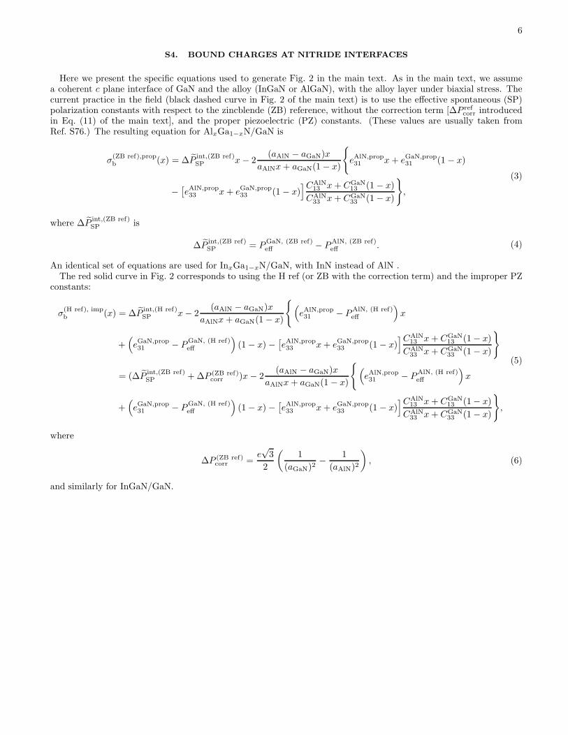
S4. BOUND CHARGES AT NITRIDE INTERFACES
Here we present the specific equations used to generate Fig. 2 in the main text. As in the main text, we assumea coherent c plane interface of GaN and the alloy (InGaN or AlGaN), with the alloy layer under biaxial stress. Thecurrent practice in the field (black dashed curve in Fig. 2 of the main text) is to use the effective spontaneous (SP)polarization constants with respect to the zincblende (ZB) reference, without the correction term [∆P ref
corr introducedin Eq. (11) of the main text], and the proper piezoelectric (PZ) constants. (These values are usually taken fromRef. S76.) The resulting equation for AlxGa1−xN/GaN is
σ(ZB ref),propb (x) = ∆P
int,(ZB ref)SP x− 2
(aAlN − aGaN)x
aAlNx+ aGaN(1− x)
eAlN,prop31 x+ eGaN,prop
31 (1− x)
−[eAlN,prop33 x+ eGaN,prop
33 (1− x)]CAlN
13 x+ CGaN13 (1− x)
CAlN33 x+ CGaN
33 (1− x)
,
(3)
where ∆Pint,(ZB ref)SP is
∆Pint,(ZB ref)SP = P
GaN, (ZB ref)eff − P
AlN, (ZB ref)eff . (4)
An identical set of equations are used for InxGa1−xN/GaN, with InN instead of AlN .The red solid curve in Fig. 2 corresponds to using the H ref (or ZB with the correction term) and the improper PZ
constants:
σ(H ref), impb (x) = ∆P
int,(H ref)SP x− 2
(aAlN − aGaN)x
aAlNx+ aGaN(1− x)
(eAlN,prop31 − P
AlN, (H ref)eff
)x
+(eGaN,prop31 − P
GaN, (H ref)eff
)(1− x)−
[eAlN,prop33 x+ eGaN,prop
33 (1− x)]CAlN
13 x+ CGaN13 (1− x)
CAlN33 x+ CGaN
33 (1− x)
= (∆Pint,(ZB ref)SP +∆P (ZB ref)
corr )x− 2(aAlN − aGaN)x
aAlNx+ aGaN(1− x)
(eAlN,prop31 − P
AlN, (H ref)eff
)x
+(eGaN,prop31 − P
GaN, (H ref)eff
)(1− x)−
[eAlN,prop33 x+ eGaN,prop
33 (1− x)]CAlN
13 x+ CGaN13 (1− x)
CAlN33 x+ CGaN
33 (1− x)
,
(5)
where
∆P (ZB ref)corr =
e√3
2
(1
(aGaN)2− 1
(aAlN)2
), (6)
and similarly for InGaN/GaN.

7
S5. DIFFERENCE BETWEEN IMPLEMENTATIONS
The difference between the current practice in the field (ZB reference, no correction term, proper PZ) and ourrevised implementation (H reference, improper PZ constants) can be determined by taking the difference of Eq. (3)and Eq. (5). For the case of AlGaN/GaN:
σ(H ref), impb (x)− σ
(ZB ref),propb (x) =x
[∆P
int,(H ref)SP −∆P
int,(ZB ref)SP
]
− 2(aAlN − aGaN)x
aAlNx+ aGaN(1− x)
[−P
AlN, (H ref)eff (x) − P
GaN, (H ref)eff (1− x)
]
=x[(
∆Pint,(ZB ref)SP +∆P (ZB ref)
corr
)−∆P
int,(ZB ref)SP
]
+ 2(aAlN − aGaN)x
aAlNx+ aGaN(1− x)
[P
AlN, (H ref)eff (x) + P
GaN, (H ref)eff (1− x)
]
=x∆P (ZB ref)corr + 2
(aAlN − aGaN)x
aAlNx+ aGaN(1− x)
[P
AlN, (H ref)eff (x) + P
GaN, (H ref)eff (1− x)
]
=x∆P (ZB ref)corr + 2ε1(x)P
AlGaN, (H ref)eff (x).
(7)
We can gain some more insight by linearizing the first term in Eq. (7):
x∆P (ZB ref)corr = x
e√3
2
(1
(aGaN)2− 1
(aAlN)2
)
= xe√3
2
1
(aGaN)2
(1− (aGaN)
2
(aAlN)2
)
= xPGaN, ZBf
(1− (aGaN)
2
(aAlN)2
)
≃ 2xPGaN, ZBf
(1− aGaN
aAlN
)
= −2PGaN, ZBf
(xaGaN − aAlN
aAlN
)
≃ −2PGaN, ZBf ε1(x)
(8)
So we see that the difference in implementations is
σ(H ref), impb (x) − σ
(ZB ref),propb (x) ≃ 2ε1(x)
[P
AlGaN, (H ref)eff (x)− PGaN, ZB
f
]
= 2ε1(x)[xPAlN, WZ
f + (1 − x)PGaN, WZf − PGaN, ZB
f
]
= 2ε1(x)[x(PAlN, WZf − PGaN, WZ
f
)+(PGaN, WZf − PGaN, ZB
f
)]
= 2ε1(x)[x(PAlN, WZf − PGaN, WZ
f
)+ P
GaN, (ZB ref)eff
]
(9)
Therefore, the difference is small for small strains, and/or when there is a large cancellation of the terms in the square
brackets. We see from Table I of the main text that PAlN, WZf − PGaN, WZ
f = 0.039 C/m2 ∼ −PGaN, (ZB ref)eff , hence
the close agreement with between the black dashed and red solid curves in Fig. 2(b) of the main text (along with the
relatively small magnitude of the strain). For the case of InGaN, P InN, WZf − PGaN, WZ
f = −0.286 C/m2 which is the
same sign as PGaN, (ZB ref)eff , hence the larger discrepancy between the black dashed and red solid curves in Fig. 2(a)
of the main text (also combined with a larger strain between InN and GaN).
[S1] D. Vanderbilt and R. D. King-Smith, “Electric polarization as a bulk quantity and its relation to surface charge,”Phys. Rev. B 48, 4442 (1993).

8
[S2] I. Vurgaftman and J. R. Meyer, “Band parameters for nitrogen-containing semiconductors,”J. Appl. Phys. 94, 3675 (2003).
[S3] H. Schulz and K.H. Thiemann, “Crystal structure refinement of AlN and GaN,” Solid State Commun. 23, 815 (1977).[S4] M. E. Aumer, S. F. LeBoeuf, B. F. Moody, and S. M. Bedair, “Strain-induced piezoelectric field effects on light emission
energy and intensity from AlInGaN/InGaN quantum wells,” Appl. Phys. Lett. 79, 3803 (2001).[S5] Q. Li, S. J. Xu, M. H. Xie, S. Y. Tong, X. H. Zhang, W. Liu, and S. J. Chua, “Strong screening effect of photo-generated
carriers on piezoelectric field in In0.13Ga0.87N/In0.03Ga0.97N quantum wells,” Jpn. J. Appl. Phys. 41, L1093 (2002).[S6] Y. D. Jho, J. S. Yahng, E. Oh, and D. S. Kim, “Measurement of piezoelectric field and tunneling times in strongly biased
InGaN/GaN quantum wells,” Appl. Phys. Lett. 79, 1130 (2001).[S7] A. Hangleiter, F. Hitzel, S. Lahmann, and U. Rossow, “Composition dependence of polarization fields in GaInN/GaN
quantum wells,” Appl. Phys. Lett. 83, 1169 (2003).[S8] S. F. Chichibu, A. C. Abare, M. S. Minsky, S. Keller, S. B. Fleischer, J. E. Bowers, E. Hu, U. K. Mishra, L. A. Coldren,
S. P. DenBaars, and T. Sota, “Effective band gap inhomogeneity and piezoelectric field in InGaN/GaN multiquantumwell structures,” Appl. Phys. Lett. 73, 2006 (1998).
[S9] P. Lefebvre, A. Morel, M. Gallart, T. Taliercio, J. Allgre, B. Gil, H. Mathieu, B. Damilano, N. Grandjean, and J. Massies,“High internal electric field in a graded-width InGaN/GaN quantum well: Accurate determination by time-resolvedphotoluminescence spectroscopy,” Appl. Phys. Lett. 78, 1252 (2001).
[S10] P. Kiesel, F. Renner, M. Kneissl, C. G. Van de Walle, G. H. Dohler, and N. M. Johnson, “Electroabsorp-tion Spectroscopy – Direct Determination of the Strong Piezoelectric Field in InGaN/GaN Heterostructure Diodes,”Phys. Stat. Sol. (a) 188, 131 (2001).
[S11] P. Kiesel, F. Renner, M. Kneissl, C. G. Van de Walle, G. H. Dohler, and N. M. Johnson, “Quantitative Analysis of Absorp-tion and Field-Induced Absorption Changes in InGaN/GaN Quantum Wells,” Phys. Stat. Sol. (b) 234, 742–745 (2002).
[S12] F. Renner, P. Kiesel, G. H. Dohler, M. Kneissl, C. G. Van de Walle, and N. M. Johnson, “Quantitative analysisof the polarization fields and absorption changes in InGaN/GaN quantum wells with electroabsorption spectroscopy,”Appl. Phys. Lett. 81, 490 (2002).
[S13] R. J. Kaplar, S. R. Kurtz, D. D. Koleske, and A. J. Fischer, “Electroreflectance studies of Stark shifts and polarization-induced electric fields in InGaN/GaN single quantum wells,” J. Appl. Phys. 95, 4905 (2004).
[S14] S.-M. Kim, H. S. Oh, J. H. Baek, K.-H. Lee, G. Y. Jung, J.-H. Song, H.-J. Kim, B.-J. Ahn, D. Yanqun, and J.-H.Song, “Effects of patterned sapphire substrates on piezoelectric field in blue-emitting InGaN multiple quantum wells,”IEEE Electr. Device Lett. 31, 842 (2010).
[S15] G. Franssen, P. Perlin, and T. Suski, “Photocurrent spectroscopy as a tool for determining piezoelectric fields inInxGa1−xN/GaN multiple quantum well light emitting diodes,” Phys. Rev. B 69, 045310 (2004).
[S16] I. H. Brown, I. A. Pope, P. M. Smowton, P. Blood, J. D. Thomson, W. W. Chow, D. P. Bour, and M. Kneissl,“Determination of the piezoelectric field in InGaN quantum wells,” Appl. Phys. Lett. 86, 131108 (2005).
[S17] M. Thomsen, H. Jonen, U. Rossow, and A. Hangleiter, “Effects of spontaneous polarization on GaInN/GaN quantumwell structures,” J. Appl. Phys. 109, 123710 (2011).
[S18] D. Turchinovich, P. Uhd Jepsen, B. Monozon, M. Koch, S. Lahmann, U. Rossow, and A. Hangleiter, “Ultrafast polariza-tion dynamics in biased quantum wells under strong femtosecond optical excitation,” Phys. Rev. B 68, 241307 (2003).
[S19] O. Gfrorer, C. Gemmer, J. Off, J. S. Im, F. Scholz, and A. Hangleiter, “Direct Observation of Pyroelectric Fields inInGaN/GaN and AlGaN/GaN Heterostructures,” Phys. Stat. Sol. (b) 216, 405–408 (1999).
[S20] E. Berkowicz, D. Gershoni, G. Bahir, A. C. Abare, S. P. DenBaars, and L. A. Coldren, “Optical spectroscopy ofInGaN/GaN quantum wells,” Phys. Stat. Sol. (b) 216, 291–300 (1999).
[S21] S. I. Park, J. I. Lee, and D. H. Jang, “Measurement of Internal Electric Field in GaN-Based Light-Emitting Diodes,”IEEE J. Quantum Elect. 48, 500 (2012).
[S22] T. Takeuchi, C. Wetzel, S. Yamaguchi, H. Sakai, H. Amano, I. Akasaki, Y. Kaneko, S. Nakagawa, Y. Yamaoka, andN. Yamada, “Determination of piezoelectric fields in strained GaInN quantum wells using the quantum-confined Starkeffect,” Appl. Phys. Lett. 73, 1691 (1998).
[S23] C. Y. Lai, T. M. Hsu, W.-H. Chang, K.-U. Tseng, C.-M. Lee, C.-C. Chuo, and J.-I. Chyi, “Direct mea-surement of piezoelectric field in In0.23Ga0.77N/GaN multiple quantum wells by electrotransmission spectroscopy,”J. Appl. Phys. 91, 531 (2002).
[S24] D. Cherns, J. Barnard, and F. A. Ponce, “Measurement of the piezoelectric field across strained InGaN/GaN layers byelectron holography,” Solid State Commun. 111, 281 (1999).
[S25] J. S. Barnard and D. Cherns, “Direct observation of piezoelectric fields in GaN/ InGaN/GaN strained quantum wells,”J. Electron Microsc. 49, 281 (2000).
[S26] L. Jia, E. T. Yu, D. Keogh, P. M. Asbeck, P. Miraglia, A. Roskowski, and R. F. Davis, “Polar-ization charges and polarization-induced barriers in AlxGa1−xN/GaN and InyGa1−yN/GaN heterostructures,”Appl. Phys. Lett. 79, 2916 (2001).
[S27] X. H. Zhang, W. Liu, and S. J. Chua, “Optical transitions in InGaN/GaN quantum wells: effects of the piezoelectricfield,” J. Cryst. Growth 268, 521 (2004).
[S28] Y. Zhang, I. P. Smorchkova, C. R. Elsass, S. Keller, J. P. Ibbetson, S. Denbaars, U. K. Mishra, and J. Singh, “Charge con-trol and mobility in AlGaN/GaN transistors: Experimental and theoretical studies,” J. of Appl. Phys. 87, 7981 (2000).
[S29] S. K. Davidsson, M. Gurusinghe, T. G. Andersson, and H. Zirath, “The influence of composition and unintentional dopingon the two-dimensional electron gas density in AlGaN/GaN heterostructures,” J. of Electron. Mater. 33, 440 (2004).

9
[S30] G. Martınez-Criado, A. Cros, A. Cantarero, O. Ambacher, C. R. Miskys, R. Dimitrov, M. Stutzmann, J. Smart, andJ. R. Shealy, “Residual strain effects on the two-dimensional electron gas concentration of AlGaN/GaN heterostructures,”J. Appl. Phys. 90, 4735 (2001).
[S31] S. C. Binari, J. M. Redwing, G. Kelner, and W. Kruppa, “AlGaN/GaN HEMTs grown on SiC substrates,”Electron. Lett. 33, 242 (1997).
[S32] Y.-F. Wu, B. P. Keller, S. Keller, D. Kapolnek, P. Kozodoy, S. P. Denbaars, and U. K. Mishra, “Veryhigh breakdown voltage and large transconductance realized on GaN heterojunction field effect transistors,”Appl. Phys. Lett. 69, 1438 (1996).
[S33] C. Nguyen, N. X. Nguyen, M. Le, and D. E. Grider, “High performance GaN/AlGaN MODFETs grown by RF-assistedMBE,” Electron. Lett. 34, 309 (1998).
[S34] L. W. Wong, S. J. Cai, R. Li, K. Wang, H. W. Jiang, and M. Chen, “Magnetotransport study on the two-dimensionalelectron gas in AlGaN/GaN heterostructures,” Appl. Phys. Lett. 73, 1391 (1998).
[S35] K. Kohler, S. Muller, P. Waltereit, W. Pletschen, V. Polyakov, T. Lim, L. Kirste, H. P. Menner, P. Bruckner, O. Ambacher,C. Buchheim, and R. Goldhahn, “Electrical properties of AlxGa1−xN/GaN heterostructures with low Al content,”J. Appl. Phys. 109, 053705 (2011).
[S36] K. Kohler, S Muller, Patrick Waltereit, L. Kirste, H. P. Menner, W. Bronner, and Rudiger Quay, “Growth and elec-trical properties applications and materials science of AlxGa1−xN/GaN heterostructures with different Al-content,”Phys. Stat. Sol. (a) 206, 2652 (2009).
[S37] A. Nakajima, Y. Sumida, M. H. Dhyani, H. Kawai, and E. M. S. Narayanan, “High Density Two-Dimensional Hole GasInduced by Negative Polarization at GaN/AlGaN Heterointerface,” Appl. Phys. Express 3, 121004 (2010).
[S38] J. Burm, W. J. Schaff, L. F. Eastman, H. Amano, and I. Akasaki, “75 A GaN channel modulation doped field effecttransistors,” Appl. Phys. Lett. 68, 2849 (1996).
[S39] T. Wang, Y. Ohno, M. Lachab, D. Nakagawa, T. Shirahama, S. Sakai, and H. Ohno, “Electron mobility exceeding 104
cm2/V s in an AlGaN/GaN heterostructure grown on a sapphire substrate,” Appl. Phys. Lett. 74, 3531 (1999).[S40] Y. Liu, M. Z. Kauser, D. D. Schroepfer, P. P. Ruden, J. Xie, Y. T. Moon, N. Onojima, H. Morkoc, K.-A. Son, and
M. I. Nathan, “Effect of hydrostatic pressure on the current-voltage characteristics of GaN/AlGaN/GaN heterostructuredevices,” J. Appl. Phys. 99, 113706 (2006).
[S41] G. J. Ding, L. W. Guo, Z. G. Xing, Y. Chen, P. Q. Xu, H. Q. Jia, J. M. Zhou, and H. Chen, “Characterization ofdifferent-Al-content AlGaN/GaN heterostructures on sapphire,” Sci. China Phys. Mech. Astron. 53, 49– (2010).
[S42] W. S. Chen, S. J. Chang, Y. K. Su, R. L. Wang, C. H. Kuo, and S. C. Shei, “AlxGa1−xN/GaN heterostructure fieldeffect transistors with various Al mole fractions in AlGaN barrier,” J. Cryst. Growth 275, 398 (2005).
[S43] K. Jeganathan, T. Ide, M. Shimizu, and H. Okumura, “Two-dimensional electron gases induced by polarization chargesin AlN/GaN heterostructure grown by plasma-assisted molecular-beam epitaxy,” J. Appl. Phys. 94, 3260 (2003).
[S44] R. Gaska, A. Osinsky, J. W. Yang, and M. S. Shur, “Self-Heating in High-Power AlGaN-GaN HFETs,”IEEE Electr. Device Lett. 19, 89 (1998).
[S45] P. M. Asbeck, E. T. Yu, S. S. Lau, G. J. Sullivan, J. Van Hove, and J. Redwing, “Piezoelectric charge densities inAlGaN/GaN HFETs,” Electron. Lett. 33, 1230 (1997).
[S46] D.-P. Wang, C.-C. Wu, and C.-C. Wu, “Determination of polarization charge density on interface of AlGaN/GaNheterostructure by electroreflectance,” Appl. Phys. Lett. 89, 161903 (2006).
[S47] A. T. Winzer, R. Goldhahn, C. Buchheim, O. Ambacher, A. Link, M. Stutzmann, Y. Smorchkova, U. K. Mishra, andJ. S. Speck, “Photoreflectance studies of N- and Ga-face AlGaN/GaN heterostructures confining a polarization induced2DEG,” Phys. Stat. Sol. (b) 240, 380 (2003).
[S48] G. Li, Y. Cao, H. G. Xing, and D. Jena, “High mobility two-dimensional electron gases in nitride heterostructures withhigh Al composition AlGaN alloy barriers,” Appl. Phys. Lett. 97, 222110 (2010).
[S49] S. Arulkumaran, T. Egawa, H. Ishikawa, and T. Jimbo, “Characterization of different-Al-content AlxGa1−xN/GaNheterostructures and high-electron-mobility transistors on sapphire,” J. Vac. Sci. Technol. B 21, 888 (2003).
[S50] O. Ambacher, B. Foutz, J. Smart, J. R. Shealy, N. G. Weimann, K. Chu, M. Murphy, A. J. Sierakowski, W. J. Schaff,L. F. Eastman, R. Dimitrov, A. Mitchell, and M. Stutzmann, “Two dimensional electron gases induced by spontaneousand piezoelectric polarization in undoped and doped AlGaN/GaN heterostructures,” J. Appl. Phys. 87, 334 (2000).
[S51] G. Franssen, J. A. Plesiewicz, L. H. Dmowski, P. Prystawko, T. Suski, W. Krupczynski, R. Jachymek, P. Perlin, andM. Leszczynski, “Hydrostatic pressure dependence of polarization-induced interface charge in AlGaN/GaN heterostruc-tures determined by means of capacitance-voltage characterization,” J. Appl. Phys. 100, 113712 (2006).
[S52] N. Grandjean, B. Damilano, S. Dalmasso, M. Leroux, M. Lagt, and J. Massies, “Built-in electric-field effects in wurtziteAlGaN/GaN quantum wells,” J. Appl. Phys. 86, 3714 (1999).
[S53] R. Cingolani, A. Botchkarev, H. Tang, H. Morkoc, G. Traetta, G. Coli, M. Lomascolo, A. Di Carlo, F. Della Sala, andP Lugli, “Spontaneous polarization and piezoelectric field in GaN/Al0.15Ga0.85N quantum wells: Impact on the opticalspectra,” Phys. Rev. B 61, 2711 (2000).
[S54] G. Chen, Z. L. Li, X. Q. Wang, C. C. Huang, X. Rong, L. W. Sang, F. J. Xu, N. Tang, Z. X. Qin, M. Sumiya, Y. H. Chen,W. K. Ge, and B. Shen, “Effect of polarization on intersubband transition in AlGaN/GaN multiple quantum wells,”Appl. Phys. Lett. 102, 192109 (2013).
[S55] C. McAleese, P. M. F. J. Costa, D. M. Graham, H. Xiu, J. S. Barnard, M. J. Kappers, P. Dawson, M. J. Godfrey, andC. J. Humphreys, “Electric fields in AlGaN/GaN quantum well structures,” Phys. Stat. Sol. (b) 243, 1551 (2006).
[S56] R. Langer, J. Simon, V. Ortiz, N. T. Pelekanos, A. Barski, R. Andre, and M. Godlewski, “Giant electric fields inunstrained GaN single quantum wells,” Appl. Phys. Lett. 74, 3827 (1999).

10
[S57] M. Leroux, N. Grandjean, M. Laugt, J. Massies, B. Gil, P. Lefebvre, and P. Bigenwald, “Quantum confined Stark effectdue to built-in internal polarization fields in (Al,Ga)N/GaN quantum wells,” Phys. Rev. B 58, R13371 (1998).
[S58] N. Suzuki and N. Iizuka, “Effect of Polarization Field on Intersubband Transition in AlGaN/GaN Quantum Wells,”Jpn. J. Appl. Phys. 38, L363 (1999).
[S59] M. Esmaeili, M. Gholami, H. Haratizadeh, B. Monemar, P. O. Holtz, S. Kamiyama, H. Amano, and I. Akasaki, “Ex-perimental and theoretical investigations of optical properties of GaN/AlGaN MQW nanostructures. Impact of built-inpolarization fields,” Opto-Electron. Rev. 17, 293 (2009).
[S60] M. Esmaeili, M. Sabooni, H. Haratizadeh, P. P. Paskov, B. Monemar, P. O. Holz, S. Kamiyama, andM. Iwaya, “Optical properties of GaN/AlGaN QW nanostructures with different well and barrier widths,”J. Phys: Condens. Mat. 19, 356218 (2007).
[S61] A. Pinos, S. Marcinkevicius, K. Liu, M. S. Shur, E. Kuokstis, G. Tamulaitis, R. Gaska, J. Yang, and W. Sun, “Screeningdynamics of intrinsic electric field in AlGaN quantum wells,” Appl. Phys. Lett. 92, 061907 (2008).
[S62] S. Marcinkevicius, A. Pinos, K. Liu, D. Veksler, M. S. Shur, J. Zhang, and R. Gaska, “Intrinsic electric fields in AlGaNquantum wells,” Appl. Phys. Lett. 90, 081914 (2007).
[S63] E. Kuokstis, C. Q. Chen, M. E. Gaevski, W. H. Sun, J. W. Yang, G. Simin, M. Asif Khan, H. P. Maruska, D. W. Hill,M. C. Chou, J. J. Gallagher, and B. Chai, “Polarization effects in photoluminescence of c- and m-plane GaN/AlGaNmultiple quantum wells,” Appl. Phys. Lett. 81, 4130 (2002).
[S64] H. M. Ng, R. Harel, S. N. G. Chu, and A. Y. Cho, “The effect of built-in electric field in GaN/AlGaN quantum wellswith high AIN mole fraction,” J. Electron. Mater. 30, 134 (2001).
[S65] J. S. Im, H. Kollmer, J. Off, A. Sohmer, F. Scholz, and A. Hangleiter, “Reduction of oscillator strength due to piezoelectricfields in GaN/AlxGa1−xN quantum wells,” Phys. Rev. B 57, R9435 (1998).
[S66] J. Simon, R. Langer, A. Barski, and N. Pelekanos, “Spontaneous polarization effects in GaN/AlxGa1−xN quantum wells,”Phys. Rev. B 61, 7211–7214 (2000).
[S67] J. Simon, R. Langer, A. Barski, M. Zervos, and N. T. Pelekanos, “Residual doping effects on the amplitude of polarization-induced electric fields in GaN/AlGaN quantum wells,” Phys. Stat. Sol. (a) 188, 867 (2001).
[S68] O. Gfrorer, T. Schlusener, V. Harle, F. Scholz, and A. Hangleiter, “Mechanisms of Strain Reduction in GaN andAlGaN/GaN Epitaxial Layers,” MRS Proc. 449, 429 (2011).
[S69] A. T. Winzer, R. Goldhahn, G. Gobsch, A. Link, M. Eickhoff, U. Rossow, and A. Hangleiter, “Determination of the polar-ization discontinuity at the AlGaN/GaN interface by electroreflectance spectroscopy,” Appl. Phys. Lett. 86, 1–3 (2005).
[S70] A. Drabinska, K. P. Korona, R. Bozek, J. M. Baranowski, K. Paku l a, T. Tomaszewicz, and J. Gronkowski, “Investigationof 2D Electron Gas on AlGaN/GaN Interface by Electroreflectance,” Phys. Stat. Sol. (c) 333, 329 (2003).
[S71] S. R. Kurtz, A. A. Allerman, D. D. Koleske, A. G. Baca, and R. D. Briggs, “Electronic properties of the AlGaN/GaNheterostructure and two-dimensional electron gas observed by electroreflectance,” J. Appl. Phys. 95, 1888 (2004).
[S72] Y.-G. Zhou, B. Shen, T. Someya, H.-Q. Yu, J. Liu, H.-M. Zhou, R. Zhang, Y. Shi, Y.-D. Zheng, and Y. Arakawa,“Investigation of the polarization-induced charges in modulation-doped AlxGa1−xN/GaN heterostructures through ca-pacitancevoltage profiling and simulation,” Jpn. J. Appl. Phys. 41, 2531 (2002).
[S73] E. T. Yu, G. J. Sullivan, P. M. Asbeck, C. D. Wang, D. Qiao, and S. S. Lau, “Measurement of piezoelectrically inducedcharge in GaN/AlGaN heterostructure field-effect transistors,” Appl. Phys. Lett. 71, 2794 (1997).
[S74] I. P. Smorchkova, C. R. Elsass, J. P. Ibbetson, R. Vetury, B. Heying, P. Fini, E. Haus, S. P. DenBaars, J. S. Speck,and U. K. Mishra, “Polarization-induced charge and electron mobility in AlGaN/GaN heterostructures grown by plasma-assisted molecular-beam epitaxy,” J. Appl. Phys. 86, 4520 (1999).
[S75] E. J. Miller, E. T. Yu, C. Poblenz, C. Elsass, and J. S. Speck, “Direct measurement of the polarization charge inAlGaN/GaN heterostructures using capacitancevoltage carrier profiling,” Appl. Phys. Lett. 80, 3551 (2002).
[S76] F. Bernardini, V. Fiorentini, and D. Vanderbilt, “Spontaneous polarization and piezoelectric constants of III-V nitrides,”Phys. Rev. B 56, R10024 (1997).