i.lampiran a - repository.wima.ac.idrepository.wima.ac.id/1624/7/lampiran.pdf · s=o no display...
TRANSCRIPT

I.lAMPIRAN A

RF
<OK
IN 1 C>--"'Ar--~
IN2
IN ,C>--"'Ar----'
VCC-12V
.'~.
Rl
-I IDOhm RESISTO R_
-L 10K
lC02 -1(1 I~PMl.O . IISS r-- VOO
J 2
= 11 1 ... 11
3 4 , 6 081 7 , 083 ~ , 10 095 11 " 09t 13 14
W ~
~ ~~.:: :;---------i~::: ~·------------___'c:=:>:.O.4
~ o;-------------~c=>:.O~
Lampiran Gambar Rangkaian Lengkap Mixing Audio Automatic

LAMPIRANB

include <at89x51.h>
#define onOffPO 0 #define sw PO 1 #define psh 1 PO _2 #define psh2 PO _3 #define psh3 PO _ 4 #define psh4 PO _ 5 #define rs PI 0 #define e PI 1 #define datalcd P2
const char kata[]="Agustinus Wijaya"; const char kata2[]=" 5103000043"; const char kata3[]="Penguatan = ";
void tunda(int loop2) {int loop;
loop=O; while (loop<=loop2) {loop++;
TH 1=(-5000/256)-1; TL 1 =(-5000%256); TFl=O; TRI=I; while (!TFI); }}
void delayMotor(int del) {onOff=l;
sw=O; tunda(del); II kira2 delay 8000 tp hampir mendekati kira2 9,8k onOff=O;}
void motorBalik(int del) {onOff=l; sw=l; tunda(del); II kira2 delay 8000 tp hampir mendekati kira2 9,8k onOff=O;}
void kirim-p(int dat) {rs=O; dataIcd=dat; e=l; e=O; tunda(3);}

void initIcdO {tunda(3); kirim --.p( 56);kirim --'p(56); kirim --'p(56);kirim --'p(56); kirim --.p( 6); kirim --.p( 12); kirim --.p( 1 ); }
void kirim k(int dat2) {rs=l; dataIcd=dat2; e=l; e=O; tunda(3);}
void cIearO {rs=O; kirim --.p( I);}
void cursorhomeO {rs=O; kirim --'p(2);}
void mainO {int a,b,c,d,buf,buf2,buf3,i;
initlcdO; kirim--'p(128); for (i=O;i<16;i++) kirim _ k(kata[i)); kirim --'p(l92); for (i=O;i<11;i++) kirim _ k(kata2[i)); tunda(5000); clearO; cursorhomeO; kirim --.p( 128); for (i=O;i<ll;i++) kirim k(kata3[i]);
onOff=l; sw=l; tunda(lOOO); onOff=O; psh 1 =psh2=psh3=psh4=O; a=5000; b=7000; c=9000;
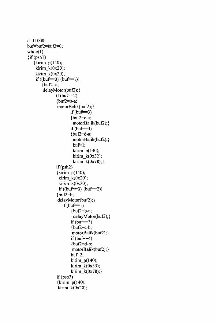
d=IIOOO; buf=buf2=buf3=O; while(l) {if(pshl)
{kirim ---.p(l40); kirim _ k(0x20); kirim _ k(Ox20); if «buf==O)II(buf=-I))
{buf2=a; delayMotor(buf2); }
if (buf==2) {buf2=b-a; motorBalik(buf2); }
if (buf=-3) {buf2=c-a;
motorBalik(buf2); } if (buf==4) {buf2=d-a; motorBalik(buf2); }
if (psh2)
buf=l; kirim ---.p(l40); kirim _ k(Ox32); kirim _k(Ox78);}
{kirim ---.p(l40); kirim _k(Ox20); kirim k(Ox20); if «buf==O)II(buf=-2»
{buf2=b; delayMotor(buf2); }
if (buf==l) {buf2=b-a; delayMotor(buf2); }
if (buf==3) {buf2=c-b; motorBalik(buf2); } if (buf==4) {buf2=d-b; motorBalik(buf2); }
buf=2; kirim ---.p( 140); kirim_k(Ox33); kirim_k(Ox78);}
if (psh3) {kirim ---.p(l40); kirim k(0x20);

kirim_k(0x20); if ((buf O)II(buf==3» {buf2=c; delayMotor(buf2); } if (buf== I) {buf2=c-a; deiayMotor(buf2); } if (buf==2) {buf2=c-b; delayMotor(buf2); } if (buf==4) {buf2=d-c; motorBalik(buf2); }
buf=3; kirimy(140); kirim_k(Ox34); kirim _k(Ox78);}
if (psh4) {kirimy(140); kirim _ k(0x20); kirim _ k(0x20); if ((buf==O)II(buf==4»
{buf2=d; delayMotor(buf2); } if (buf=-l) {buf2=d-a; delayMotor(buf2); } if (buf==2) {buf2=d-b; deiayMotor(buf2); } if (buf==3) {buf2=d-c; delayMotor(buf2); } buf=4; kirimy(140); kirim_k(Ox35); kirim_k(Ox78);}} }

LAMPlRANC

Instruction Table LCD
Instruction Code
Instruction Description Execution time
(fo!lC='270Khz) RS RIW DB7 DB6 DB5 DB4 DB3 DB2 DBI DBa
Clear Display a a a a a a a a a I Write "'OOH" to DDRAM and set
DDRAM address to "OOff' from AC 1.53ms
Set DDRAM address to ''OOff' from AC
RetumHome a 0 a a a a a 0 I -and return cursor to its original position i
1.53ms shifted. The contents ofDDRAM are not
changed
Entry Mode 0 0 a 0 0 0 a I lID SH
ASSign cursor moving direction and 39/1 S
Set enable the shift of entire display.
Display Set display (D), cursor (C), and blinking
ONIOFF a 0 a a a a I D C B 39/1s
Control of cursor (B) on/off control bit.
Cursor or Set cursor moving and display shift
0 0 a 0 0 I SIC RfL - - control bit, and the direction, without 39/1 s Display Shift
changing of DDRAM data
Set interface data length (DL:8-bitl4-bit),
Function Set 0 0 0 0 I DL N F - - numbers of display line 39/1 s
(N:2-linell-line)and, display font type (F:5xll dots/5x8 dots)
SetCGRAM 0 0
Address 0 I AC5 AC4 AC3 AC2 ACI ACO Set CGRAM address in address counter. 39/1 S
SetDDRAM 0 0 I AC6 AC5 AC4 AC3 AC2 ACI ACO 39/1 S
Address Set DDRAM address in address counter.
Read Busy Whether during internal operation or not
Flag and 0 I BF AC6 AC5 AC4 AC3 AC2 ACI ACO can be known by reading BF The
O/1S
Address contents of address coWlter can also be
read.
Write Data to I 0
RAM D7 D6 D5 D4 D3 D2 DI DO
Write data tnto internal RAM
(DDRAMlCGRAM). 43/1 S
Read Data I I D7 D6 D5 D4 D3 D2 DI DO
Read data from internal RAM 43/1 s
from RAM (DDRAMlCGRAM).
110 = 1 Increment C=1 Cursor ON RlL = 1 : Right Shift F=O 5x7 Dots
1/0= 0 Decrement C=O Cursor OFF RIL = 0 : Left Shift F=1 5x10 Dots
S = 1 Display shift B = 1 Blink ON DL=1 :8BiIs BF = 1: Busy
S=O No display shift B=O Blink OFF DL=0:4BiIs BF " 0: Can Accept Data
0=1 Display ON SIC = 1 Display Shift N=1:2Lines ACG CG RAM Address
0=0 Display OFF SIC = 0 Cursor Move N = 0: 1 Line ADD DO RAM Address
: don't care

LAMPlRAND

80135/137/139
Medium Power Linear and Switching Applications • Complement to BD136, BD138 and BD140 respectively
1 TO-126
1. Emitter 2.Collector 3.Base
NPN Epitaxial Silicon Transistor
Absolute Maximum Ratings T e=25°C unless otherwise noted
Symbol Parameter Value Units
VeBO Collector-Base Vollage : BD135 45 V : BD137 60 V : BD139 80 V
VCEO Collector-Emitter Vollage : BD135 45 V : BD137 60 V : BD139 80 V
VEBO Emitter-Base Vollage 5 V
Ic Collector Current (DC) 1.5 A
Icp Collector Current (Pulse) 3.0 A
IB Base Current 0.5 A
Pc Collector Dissipation (T c=25°C) 12.5 W
Pc Collector Dissipation (T.=25°C) 1.25 W
TJ Junction Temperature 150 °C
TSTG Storage Temperature - 55 -150 °C
Electrical Characteristics T e=25°C unless otherwise noted
Symbol Parameter Test Condition MIn. Typ. MIx. UnII8
VCEQ(sus) Collector-Emitter Sustaining Voltage : BD135 Ic = 30mA, IB = 0 45 V : BD137 60 V : BD139 80 V
ICBO Collector Cut-off Current VeB = 3OV, IE = 0 0.1 I1A lEBO Emitter Cut-olf Current VEa = 5V, Ic = 0 10 I1A hFE1 DC Current Gain : ALL DEVICE VCE = 2V, Ie = 5mA 25
hFE2 : ALL DEVICE VeE = 2V, Ie = 0.5A 25
hFE3 : BD135 VCE = 2V, Ic = 150mA 40 250 : BD137, BD139 40 160
VCE(sat) Collector-Emitter Saturation Voliage Ic = 500mA, la = 50mA 0.5 V
VaE(on) Base-Emitter ON Voliage VCE = 2V, Ic = 0.5A 1 V
hFE Classification Classification 6 10 16
40 - 100 63 - 160 100 - 250
Rev_ A, Feoruary 2000

Typical Characteristics
ON
W ... ; .. ... z « ~ >-z w a: a:
g ... z 0
~ ...
:::l ... >-
:::l Ll
« '" '" Ll
" Cl
~ 20
'"
5 '" t '00
10 J .. • • 10 100 '000 ". .. , .. , "
IdmA). COLLECTOR CURRENT IdAI. COUECTOR CURRENT
Figure 1. DC current Gain Figure 2. Collector-Emltter Saturation Voltage
1.1 "r-----------------------------, W 1A OJ
k MAX. (pulsed)
f!'. •• Ie MAX. (ContlnIWUS) ~
0 .. > '" OJ W >-!:: •• :> w W .. '" «
IA m .. ,
~ .. • > .. '.1 1E. "" '.' "
.~~,-------------=~-------L~~=-~
lelA). COLLECTOR CURRENT v~, COLLECTOR·EMITIER VOLTAGE
Figure 3. Base-Emitter Voltage Figure 4. Sefe Operating Area
... '"
z
i ". i;; <II 0 0:
~ 0 I>.
~ 170
T orCI. CASE TEMPERATURE
Figure 5. POMlr Derating
Rev. A, FetInIary 2OCIO

Package Demensions
83.20 to.10
O.75tO.10_
1.60t010
0.75 to.10
2.2SlYP [2.28±O.20J
C2000 FairchIld 5emleor!duetor International
8.00 to.30
l I-
- -
#1
n tT11 0
TO-126
~ 0 N
-j
iil !ii <D 0 <'i
2.28lYP [2.28±O.20J
0
" ~ 0 C! --
0
" ~ 0
cD
3.25 to.20
(1.00) (0.50)
1.75 to.20
O.50~~
Dimensions in Millimeters
Rev. A, Feoo.y 2000
DJ C .... w S!! .... w :::::! .... w CD

TRADEMARKS
The following are registered and unregistered trademarks Fairchild Semiconductor owns or is authorized to use and is not intended to be an exhaustive list of all such trademarks.
ACEx™ Bottomless TM CoolFETTM CROSSVOL TTM E2CMOSTM FACTTM FACT Quiet Series™ FASr® FASTr™ GTOTM
DISCLAIMER
HiSeCTM ISOPLANARm MICROWlREm Popm PowerTrench® QFETm Qsm Quiet Series TM SuperSOTm-3 SuperSOTm-6
SuperSOTm-8 SyncFETm TinyLogic TM UHcm vex'"
FAIRCHILD SEMICONDUCTOR RESERVES THE RIGHT TO MAKE CHANGES WITHOUT FURTHER NOTICE TO ANY PRODUCTS HEREIN TO IMPROVE RELIABILITY, FUNCTION OR DESIGN. FAIRCHILD DOES NOT ASSUME ANY LIABILITY ARISING OUT OF THE APPLICATION OR USE OF ANY PRODUCT OR CIRCUIT DESCRIBED HEREIN; NEITHER DOES IT CONVEY ANY LICENSE UNDER ITS PATENT RIGHTS, NOR THE RIGHTS OF OTHERS.
LIFE SUPPORT POLICY
FAIRCHILD'S PRODUCTS ARE NOT AUTHORIZED FOR USE AS CRITICAL COMPONENTS IN LIFE SUPPORT DEVICES OR SYSTEMS WITHOUT THE EXPRESS WRITTEN APPROVAL OF FAIRCHILD SEMICONDUCTOR INTERNATIONAl. As used herein:
1. life support devices or systems are devices or systems Which, (a) are intended for surgical implant into the body, or (b) support or sustain life, or (c) whose failure to perform when property used in accordance wtth instructions for use provided in the labeling, can be reasonably expected to resuK in significant injury to the user.
PRODUCT STATUS DEFINmONS
Definition of Tenns
Datasheet Identification
Advance Information
Preliminary
No Identification Needed
Obsolete
02000 Fairchik:! 8em/OOfldudor International
Produc:t Status
Fonnative or In Design
First Production
Full Production
Not In Production
2. A cmical component is any component of a life support device or system whose failure to perform can be reasonably expected to cause the failure of the life support device or system, or to affect tts safety or effectiveness.
DefinlUon
This detasheet contains the design specifications tor product development. Specifications may change in any manner without notice.
This datasheet contains pre~minary data, and supplementary data will be published at a later date. Fairchild Semiconductor reserves the right to make changes at any time without notice in order to improve design.
This detasheet contains final specifications. Fairchild Semiconductor reserves the right to make changes at any time without notice in order to improve design.
This datasheet contains specifications on a product that has been discontinued by Fairchild semiconductor. The detasheet is printed tor reference information only.
Re'I.E

LAMPIRANE

f}1National Semiconductor November 1994
LM741 Operational Amplifier General Description The LM741 serieS are general purpose operetlontll amplifiers which feature improved performance over industry standards Uke the LM709. They are dlrect, plug';n nepl80ements for the 709C, LM201, MCI439 and 748 in most applications.
The amplifiers offer many features which make their appncation near1y fOOproof: overload protection on the input and
Schematic Diagram
outpUt. no latch-up when the oommon mode range Is exceeded. as well as freedom !rom oscill8tions.
The LM741C/LM741E "'" identical to the LM741/LM741A except that the LM741C/LM741E have thair performance guaranteed over a O"C to + nrc temperature range, insteed of ~ 55'<: to + 125"C.
r-~ __________ ~ ____ 1-____________ ~ ________ ~7 ~
.............,3 II'IIT
RI 1<
R3 50<
®1~5N~~COrpor8IIon TUH/9;l41
R4 5.
OIIMI Nulling ClrcuR
OUTPUt
RI2 50<
Tl/H/9341-7
R11 50
lit 25
4.,. TUH/9341-1
FlFIo.a3OMl151Pr\r111d in U. S. A.
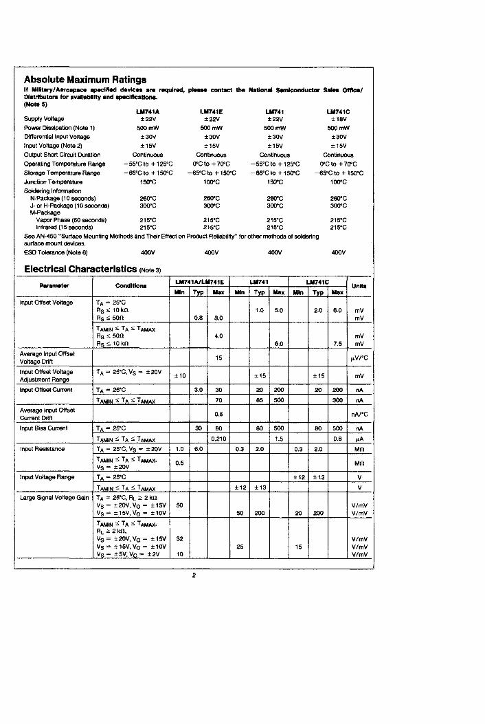
Absolute Maximum Ratings " Militaryl Aerospace speclfted devices ant required, p_ contact the Natio"", SemIconductor Sales 0IIIce1 Distributors lor ovalillbllity and speclllcations. (Nota 5)
Ul741A Ul741E Ul741 Ul741C Supply Voltage ±22V ±22V ±22V ±18V
""-Dissipation (Nole I) 500mW 500mW 500mW 500mW
DIfferentia/Input Voltage ±30V ±30V ±3OV ±30V
Input Voltage (Note 2) ±I5V ±I5V ±I5V ±I5V
Output Short Circu~ Duration Continuous ConUnuous Continuous Continuous
Operating Temperature Range - 55'C to + 125"C COCto +7COC -55'C to + I 25'C COC to +7COC
Storage Temperature Range -65'C to + 1500C -65'C to + 1500C -65'C to + 1500C -65'Cto +I50'C
Junction Temperature 1500C IWC 1500C IWC
Soldering Information N-Package (10 seconds) 260'C 260'C 260'C 260'C J. or H-Pact<age (10 seconds) 3000C 3000C 3000C 3000C M·Package
Vapor Phase (80 seconds) 215'C 215'C 215'C 215'C Infrared (15 seconds) 215'C 215'C 215'C 215'C
See AN-45O "Surface Mounting Methods and Their Effect on Product Reliability" for other methods of soldering surlace mount devices.
ESC T o/erance (Nole 6) 400V 400V 400V 400V
Electrical Characteristics (Note 3)
Parameter Conditions Ul741A1U1741E L11741 Ul741C
Unlto MIn Typ Mu -Typ MIIx Min Typ MIIx
Input Offset Voltage TA = 25"C Rs s; 10 kll 1.0 5.0 2.0 6.0 mV Rs S; 50Il 0.8 3.0 mV
TAMIN s TA::;; TAMA)( Rs s; 5011 4.0 mV Rs s; 10 kll 6.0 7.5 mV
Average Input Offset IS "V/'C Voltage Drift
Input Offset Vo~ge TA = 2S'C, Vs = ±2OV ±IO ±IS ±IS mV
Adjustment Range
Input Offset Current TA = 25"C 3.0 30 20 200 20 200 nA
TAMIN S; TA S; TAMAX 70 85 500 300 nA
Average Input Offset 0.5 nA/'C
Current Drift
Input Bias Current TA = 25"C 30 80 80 500 80 500 nA
TAMIN::;; TA s TAMAX 0.210 I.S O.B ",A
Input Resistance TA = 2S'C, Vs = ±20V 1.0 6.0 0.3 2.0 0.3 2.0 Mil
TAMIN:;;; TA s TAMAX. 0.5 Mil
Vs = ±2OV
Input Voltage Range TA=25"C ±12 ±I3 V
TAMtN::;; TA:::;;;' TAMAX ±I2 ±I3 V
Large Signal Vo~ Gain T A = 25'C, RL " 2 kll VS= ±20V.VO= ±ISV 50 V/mV VS= ±I5V,VO= ±IOV 50 200 20 200 V/mV
TAMIN ::;; TA ~ TAMAX.
RL " 2 kll, Vs = ±2OV, Vo = ±15V 32 V/m'l Vs = ±I5V, '10 = ±10V 25 15 V/mV 'Is = ±5V, Vo = ±2V 10 V/mV
2

Electrical Characteristics (Note 3) (Continued)
Parameter COnditions LM741A1LII741E LM741 LM741C
Untt8 .... Typ Max .... Typ Max .... Typ Max
Output Voltage SwIng Vs ~ ±2OV
RL" 10 kn ±16 V
RL'" 2kn ±15 V
Vs - ±15V RL "'10kO ±12 ±14 ±12 ±14 V RL'" 2kO ±10 ±13 ±10 ±13 V
Output Short Circuit TA ~ 25'C 10 25 35 25 25 rnA CUrrent TAMIN::;;: TA,s; TAMAX 10 40 mA
Commoo-Mode TAMIN ,;; TA';; TAM""
Rejection Ratio Rs';; 10kn. VCM - ±12V 70 90 70 90 dB Rs " SOO. VCM ~ ± 12V 80 95 dB
Supply Voltage Rejection TAMIN';; TA';; TAMAl<.
Ratio Vs- ±20VloVs- ±5V Rs';; son 86 96 dB Rs';; 101d} 77 96 77 96 dB
Transient Response TA - 25'C. Unity Gain Rise Time 0.25 0.8 0.3 0.3 ,... Overshoot 6.0 20 5 5 %
Bandwidth (Note 4) TA = 25°C 0.437 1.5 MHz
Slew Rate T A = 25·C. Unity Gain 0.3 0.7 0.5 0.5 VI,...
Supply Current TA = 25'C 1.7 2.8 1.7 2.8 mA
Po_ Consumption TA = 25"C Vs = ±2OV 60 ISO mW
Vs - ±15V SO 85 SO 85 mW
LM741A Vs - ±20V TA = TAMIN 185 mW
TA - TAMAl< 135 mW
LM741E Vs = ±20V
TA = TAMIN ISO mW
TA - TAMAl< ISO mW
LM741 Vs - ±15V TA - TAMIN 60 100 mW
TA ~ TAMAl< 45 75 mW
Note 1: For operation at elevated ternperaturas. th8&e devices m.I8I: be derated baaed on therma! resistance, and TJ max.. (listed IXlder "Absotute MaxImum Ratings"). Tj = T A + (6}A Po). -"- _(01) DI'(N) HOI(H} ..... "')
9jA (Junction to Arnbiant) 100'CIW l00"ClW 17fY'C1W 195'"C1W
9JC (Junction to CUe) NIA NlA 2S'C1W N/A
Note 2: FOf supply vottages less than ± lSV, the ab80IuIe mPinun input voICaga it equal to the *'4IP*Y voltage.
NoN 8: Unless 0IhtlnIIige specffied, these specifications appty tor Vs = ±l5V, -5B"C s; TA S; +1~ (lM7.411L.M741,t\). For the LM741C/lM741E. these spedf\catiOns are IIITWted 10 ~C S; T A S; + 7O"C.
Not. 4: Ga/cutUed value from: BW (MHz) - O.35/Ri8e Tirne(lA.8).
Note 5: For military specifications see RETS741X for LM741 and RETS741AX tor LM741A.
Note 6: Human body model, 1.5 kG in series with 100 pF.
3

Connection Diagrams
_ Can Package
He
TUH/Q3.41-2
Order Number LM741K. LM741K/883" f LM741AH/883 or LM741CH
See NS Package Number H08C
IluII-In-LIM or 5.0. Package
0ITSEl NUl.!.
INV£RTlNG INPUT
NOII-iNVERlING INPUT
Me
OO11'\JT
OfFSET NULL
TUH/9341-3
oro. _ LM741J, LM741J/883, LM741CM, LM741CN or LM741EN
See NS PaCkage Number J08A, M08A or N08E
-LM741 H is avaiIab6a per JM3851 011 01 01
Ne Me
He He
+ OfFSET MULL tIC
-IN v. "N OUT
v- - OfFSET NULL
tIC tIC
TlIH/9341_S
oro. Number LMnlJ-14/883+, LM741AJ-14/883" See NS Package Number Jl4A
·aIso available per JM38510/10101
.. atso ;willable per JM38510/10102
NC
NC
V+
OUTPUT
~--1. _____ .r-- -oFFSET NULL
Ordw Number LM741W/883 See NS Package _ Wl0A
nlH/93041-6

Physical Dimensions inches (millimeters)
..!:.!!!.. TTP 12.501)
""''''''''.
5
Physical Dimensions inches (millimeters) (Continued)
10.010 TYP
RO.025 TYP
t 0.220 0.211
I
GlASS SEALANT
0.310 WAX 0lASS
I
0.200 H=l:;::::;:j::;:-J:9Ft<69Ftl r :::!: ~
U1C1-U20 if.3ij::Uzj'i
--L( "I .!:1!!IIAX iii I ~~n)
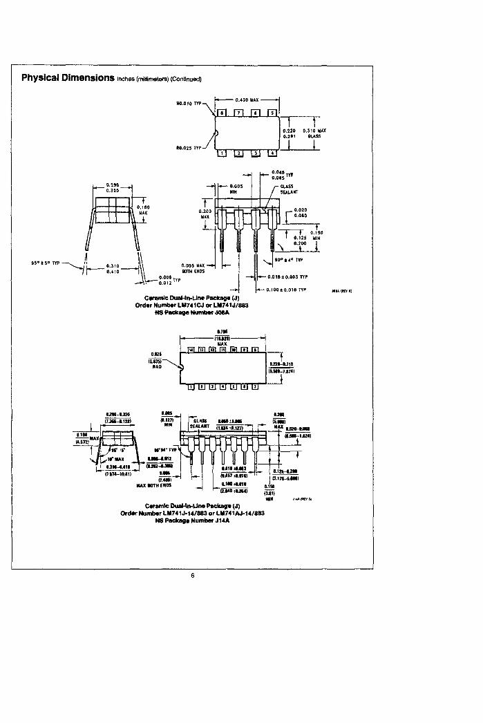
j CeramIc DuaI-In-Une p-.ge (J)
Order Number lM741CJ orlM741J/883 NS ___ J08A
,m IOJ"I
•• D
.-iiAiii MAX MlTH ENDS
CeramIc Dual-ln-Une PIIckage (J) Orda< Number lM741J·14/883 or lM741AJ·14/883
NS_age Number JI4A
6
..........----- 0.150 I O.1Z5 NIN
O·rO I
Physical Dimensions inches (milfimeters) (Continued)
D.l .. _ .... ,.,
.. OA-....
\1· .. ~-~'·~~:::::J~~~~~: ... :Ii~~~·:::~
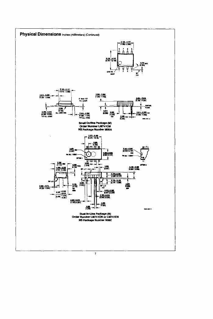
Small 011_ Package (II) Ord« Number Ul741C11
NS Package Number II08A
DwII-In-Une __ (N)
Order Number LII741CN Ol'LII741EN NS __ Number N08E
7
........ ~7 fU1JU:
""1II.ll1Sn
I

Physical Dimensions inches (millimet ..... ) (Continued)
0.080 _ t-0.055
~:~~~ -TYP
UFE SUPPORT POUCY
~ •• 27D WAX.
••• 5 •• o.~~ - Hi'" ~ 0.005 WIN TYP
, , 10 6nt_--.
0.1,0
I 0.210 WAX
GlASS
T r-DETAILA~
PIN.1 J IDENT
0.250
5
J L- 0.045 WAX -TYP
I~ CW8rnIc FI8tpek (W) Order_LM74IW/883 NS Package _ WIOA
l.u 0.008
DETAil A
"lOA (ltV E)
NATIONAL'S PRODUCTS ARE NOT AUTHORIZED FOR USE AS CRITiCAL COMPONENTS IN ul"E SUPpoRT DEVICES OR SYSTEMS WITHOUT THE EXPRESS WRITTEN APPROVAL OF THE PRESIDENT OF NATIONAL SEMICONDUCTOR CORPORATION. As used herein:
I. ute suppori devices or systems are devices or systems which. (8) are intended for surgical Implant Into the body, or (b) support or sustain life, and whose failure to perlorrn, wIlan properly used in accordance with instructions for use provided in the labeting. can be reasonably expected 10 resufi in a slgnificanl injury to the user.
2. A aiIicaI component is any component of a life support device or system whose talIura to perlorm can be reasonably expected to cause the failure of the life support _ or system, or to affect Its aafety or effectiveness.
fUtianIII Sea dCc:iiCILIdOr
~a.dinRo¥l Artngton, TX 76017 Tel: 1(800) 27~ Fax: 1(800) 737·7018
............ Ii:ooIJICCD' - Fmc- (+49) 0-18()..530 85 86 EmaI: cnjwg6el8Ym2..nec.com
Deutsch Tel: (+049) 0-1Il0-530 85 85 English Tel:: (H$) 1).180-532 78 32 F~ Tel: (+49) M8().532 93 58 ItlIIiano Tet (H9) 0-180-534 16 80
N.tionII...,oIecc :to _ ......... 131h Aoor, S*'II9II: BkIck, Ooean ~ 5 cnon Ad. TIimIhatU, Kowloon --Tet: (852) 273M600 Fax (852) 273&-9960
......... NocM~ido' _LId. Tet:81~ Fax:81~

LAMPIRANF'

!stures ompatible with MC5-S1®Products K Bytes of In-System Programmable (ISP) Flash Memory - Endurance: 1000 WritelErase Cycles
,OV to S.SV Operating Range ully Static Operation: 0 Hz to 33 MHz hree-Ievel Program Memory Lock 28 x 8-blt Internal RAM 2 Programmable VO Lines we 16-bit Timer/Counters Ix Interrupt Sources ull Duplex UART Serial Channel ow-power Idle and Power-down Modes Iterrupt Recovery from Power-down Mode latchdog Timer 'ual Data Pointer ower-off Aag ast Programming Time lexible ISP Programming (Byte and Page Mode)
~scription
1 AT89S51 is a low-power, high-performance CMOS 8-bit microcontroller with 4K ElS 01 in-system programmable Flash memory. The device is manufactured using lei's high-density nonvolatile memory technology and is compatible with the indusstandard 80C51 instruction set and pinout. The on-chip Flash allows the program mory 10 be reprogrammed in-system or by a conventional nonvolatile memory prommer. By combining a versatile 8-bit CPU with in-system programmable Flash on a nolithic chip, the Atmel AT89S51 is a powerful microcontroller which provides a hly-flexible and cost-effective solution to many embedded control applications.
1 AT89S51 provides the following standard features: 4K bytes of Flash, 128 bytes of M, 321/0 lines, Watchdog timer, two data pOinters, two 16-bit timer/counters, a five:tor two-level interrupt architecture, a full duplex serial port, on-chip oscillator, and ck circuitry. In addition, the AT89S51 is deSigned with static logic for operation vn to zero frequency and supports two software selectable power saving modes. 1 Idle Mode stops the CPU while allowing the RAM, timer/counters, serial port, and Irrupt system to continue functioning. The Power-down mode saves the RAM conIs but freezes the oscillator, disabling all other chip functions until the next external Irrupt or hardware reset.
8-bit Microcontroller with 4K Bytes In-System Programmable Flash
AT89S51
Preliminary
Rev. 2487A-10101

n Configurations
PDIP
(MaSI) Pl.S '
(MISO) P1.6
P1.0 1 P1.1
P1.4
(MOSl) PL5; 6
(MISO)Pl.6
(SCK) Pl.7
RST 9 (RXD) P3.0
(TXD) P3.1
(INTO) P3'>
(INn) P3.3 (TO) P3.4
(Tl) P3.S
(WR)P3.6'
(AO) P3.7
XTAl.2
XTAL1
GND
(SCK) Pl.7 3
NC 6
(TXD) P3.l
(INTO) P3.2
(INT1) P3.3
(TO) P3.4
(Tl) P3.S
TQFP
AT89S51
vee PO.O (ADO)
PO.1 (AD1)
PO.2 (AD2)
PO.3 (AD3)
PO" (AD4)
PO.S(ADS)
PO.6 (AOS)
J PO.7 (AD7)
EANPP , AlE/PROG PSEN
I P2.7 (A15)
P2.6 (A14)
P2.5 (A13)
P2.4 (A12)
'P2.3 (Al1)
. P2.2 (Al0)
P2.l (AS)
P2.0 (AS)
PO.4 (A04)
PO.S (AOS)
PO.S (ADS)
PO.7 (A07)
E"ANPP NC ALEIPR'OO P$EN P2.7 (A1S)
P2.6 (M4) P2.S (A13)
(MOSI)P1.5
(MISO) Pl.6
(SCK) Pl.7
RST
(RXD) P3.0
NC
(TXD) P3.l
(INTO) P3.2
(lNT1) P3.3
(TO) PH (Tl) P3.S
PLCC
PO.4(AD4)
PO.S (ADS)
PO.S(ADS)
PO.7(AD7)
EANP? NC AlEJPAOG
PSEN
P2.7 (A1S)
P2.6 (A14)
P2.S (A13)
2487 A-l 0/01

ock Diagram PO.O - PO.7 P2.0 - P2.7
.----,
~. $ , J
'WLU"I INTERRUPT, SERIAL PORT, AND TIMER BLOCKS
PSEN .--;.-LEiPROG ++"EJ\ I Vpp
TIMING INSTRUCTION ~ __ L-.--1L-__ -+--.....Y:T---~ CO~~L REGISTER
RST -r-.'L----,..-,r--L __ ...J
,7A-10/01
I~ ~
~ y
P1.0 - P1.7
AT89S51
BUFFER
I I
-1 H PROGRAM
COUNTER
I
r J L-1 DUALDPTR
PROGRAM LOGIC
3

n Description
:c
10
rtO
rt1
Supply voltage.
Ground.
Port 0 is an 8-bit open drain bidirectional I/O port. As an output port, each pin can sink eight TTL inputs. When 1 s are written to port 0 pins, the pins can be used as high-impedance inputs.
Port 0 can also be configured to be the multiplexed low-order address/data bus during accesses to external program and data memory. In this mode, PO has intemal pull-ups.
Port 0 also receives the code bytes during Flash programming and outputs the code bytes during program verification. External pull-ups are required during program verification.
Port 1 is an 8-bit bidirectional I/O port with internal pull-ups. The Port 1 output buffers can sink/source four TTL inputs. When 1 s are written to Port 1 pins, they are pulled high by the internal pull-ups and can be used as inputs. As inputs, Port 1 pins that are externally being pulled low will source current (IIJ because of the internal pull-ups.
Port 1 also receives the low-order address bytes during Flash programming and verification.
Port Pin ' Alternate Functions
Pl.5 MOSI (used for In-5ystem Programming) _.
Pl.6 MISO (used for In-System Programming)
P1,7 SCK (used for In-System Programming)
Port 2 is an 8-bit bidirectional I/O port with internal pull-ups. The Port 2 output buffers can sink/source four TTL inputs. When 1 s are written to Port 2 pins, they are pulled high by the internal pull-ups and can be used as inputs. As inputs, Port 2 pins that are extemally being pulled low will source current (IIJ because of the intemal pull-ups.
Port 2 emits the high-order address byte during fetches from external program memory and during accesses to external data memory that use 16-bit addresses (MOVX @ DPTR). In this application, Port 2 uses strong internal pull-ups when emitting ls. During accesses to external data memory that use 8-bit addresses (MOVX @ RI), Port 2 emits the contents of the P2 Special Function Register.
Port 2 also receives the high-order address bits and some control signals during Flash programming and verification.
Port 3 is an 8-bit bidirectional I/O port with internal pull-ups, The Port 3 output buffers can sink/source four TTL inputs. When 1s are written to Port 3 pins, they are pulled high by the internal pull-ups and can be used as inputs. As inputs, Port 3 pins that are extemally being pulled low will source current (IIJ because of the pull-ups.
Port 3 receives some control signals for Flash programming and verification.
Port 3 also serves the functions of various special features of the A T89S51, as shown in the following table.
AT89S51 24B7A-10101

_ElPROG
vvpp
iAL1
7A-1 0/0 1
AT89S51
Port Pin Alternate Functions
P3.0 ! RXD (serial input port) ----_. __ ._-,"-
P3.1 I TXD (serial output port) I -
P3.2 I INTO (external interrupt 0) ~- .-~--.-
P3.3 INT1 (external interrupt 1)
P3.4 TO (timer 0 external input) ~-
P3.5 T1 (timer 1 external input)
P3.6 i WR (external data memory write strobe)
P3.7 RD (external data memory read strobe)
Reset input. A high on this pin for two machine cycles while the oscillator is running resets the device. This pin drives High for 98 oscillator periods after the Watchdog times out. The OISRTO bit in SFR AUXR (address 8EH) can be used to disable this feature. In the default state of bit DISRTO, the RESET HIGH out feature is enabled.
Address Latch Enable (ALE) is an output pulse for latching the low byte of the address during accesses to external memory. This pin is also the program pulse input (PROG) during Flash programming.
In normal operation, ALE is emitted at a constant rate of 1/6 the oscillator frequency and may be used for external timing or clocking purposes. Note, however, that one ALE pulse is skipped during each access to external data memory.
If desired, ALE operation can be disabled by setting bit 0 of SFR location 8EH. With the bit set, ALE is active only during a MOVX or MOVe instruction. Otherwise, the pin is weakly pulled high. Setting the ALE-disable bit has no effect if the microcontroller is in external execution mode.
Program Store Enable (PSEN) is the read strobe to external program memory.
When the AT89S51 is executing code from external program memory, PSEN is activated twice each machine cycle, except that two PSEN activations are skipped during each access to external data memory.
External Access Enable. EA must be strapped to GNO in order to enable the device to fetch code from external program memory locations starting at OOOOH up to FFFFH. Note, however, that if lock bit 1 is programmed, EA will be internally latched on reset.
EA should be strapped to V cc for internal program executions.
This pin also receives the 12-volt programming enable voltage (Vpp) during Flash programming.
Input to the inverting oscillator amplifier and input to the internal clock operating circuit.
Output from the inverting oscillator amplifier
5

leeial netion 'gietere
A map of the on-chip memory area called the Special Function Register (SFR) space is shown in Table 1.
Note that not all of the addresses are occupied. and unoccupied addresses may not be implemented on the chip. Read accesses to these addresses will in general return random data, and write accesses wiU have an indeterminate effect.
Ie 1. AT89S51 SFR Map and Reset Values
IF8H l I I i I OFFH
, B I I \ I ::f =0 i-·r II I: EOHra~~ooi I , I I I I 10E7H
1-.1
.--1- -t I I~ 1 I D8H ~PSW+~~--~--'-II ---, t T----+ --j OOFH
)OH 1,1 QQOOQQQQ :, I r I L- 1 007H If---- ,I . -----1 ~8H I I I Iii [ I I
r---~~_+----t- i t- I t-- + I OCFH
~oHI :, ! I I Ii 1 I 'loC7H
-I -'1P I --+ I -t I -+ ! '~-I 38H I XXOOOOOO I +_~_~ I -L~~-L I ~ OBFH
lOH l~11~;2.1.1L! I ! [ i I I OB7H
,eH I oxo~ooo I :--i--I--~l t---~\--j OAFH
I P2 I r AUXR1! I I I I, I OH I I ' I i WDTRST I I
1 11111111 , ! xxxxxxxo , I xxxxxxxx ~ 1 OA7H
8H ~CON I. SBUF ! I I I I . , I
i o~~oo i xxxxxxxx: I i I -4---J 9FH
H ~~12.l.J I \ I I' I 97H
i TCON 1 TMOD TlO I Tl1 I TH1 I . -----1 H l 00000000 I 00000000 00000000 I 00000000 oooooooo XX~~~O 8FH
H I PO I SP OPOl ! 11111111' 00000111 00000000 OP1H PCON
oooooooo OXXXOOOO 87H
AT89S51 __________________________ ...
24B7A-10/0l

7A-10/01
AT89S51
User software should not write 1 s to these unlisted locations, since they may be used in future products to invoke new features. In that case, the reset or inactive values of the new bits will always be O.
Interrupt Registers: The individual interrupt enable bits are in the I E register. Two priorities can be set for each of the five interrupt sources in the IP register.
Table 2. AUXR: Auxiliary Register
AUXR Address = 8EH Reset Value = XXXOOXXOB
Not Bit Addressable
Bit
DISALE
DISRTO
WDIDLE
WDIDLE
o
Reserved for future expansion
Disable/Enable ALE
DISALE
Operating Mode
o ALE is emitted at a constant rate of 1/6 the oscillator frequency
ALE is active only during a MOVX or MOVe instruction
DisablelEnable Reset out
DISRTO
o Reset pin is driven High after WDT times out
Reset pin is input only
DisablelEnable WDT in IDLE mode
WDT continues to count in IDLE mode
WDT halts counting in IDLE mode
Dual Data Pointer Registers: To facilitate accessing both internal and external data memory, two banks of 16-bit Data Pointer Registers are provided: DPO at SFR address locations 82H-83H and DP1 at B4H-85H. Bit DPS = 0 in SFR AUXR1 selects DPO and DPS = 1 selects DP1. The user should always initialize the DPS bit to the appropriate value before accessing the respective Data Pointer Register.
7

!mory "ganization
ogram Memory
ta Memory
tchdog er
ne-time abled with set-out)
Power Off Flag: The Power Off Flag (POF) is located at bit 4 (PCON.4) in the PCON SFR. POF Is set to "1" during power up. It can be set and rest under software control and is not affected by reset.
Table 3. AUXR1; Auxiliary Register 1
AUXR1 Address = A2H
Not Bit Addressable
Reset Value = XXXXXXXOB
Bit 'I ~~~~~~~~6~. .., 5 _-_Tl~~4-'I- -_3--_·~ __ -2 __ 1LI-_-_-_-. _··-_--+-..Li_~-__ ~_P-O-S_-_.~-_..Jj
Reserved for future expansion
DPS Data Pointer Register Select
DPS
o Selects DPTR Registers DPOl, DPOH
Selects DPTR Registers DP1 l, DP1 H
MCS-51 devices have a separate address space for Program and Data Memory. Up to 64K bytes each of external Program and Data Memory can be addressed.
If the EA pin is connected to GND, all program fetches are directed to external memory.
On the AT89S51, if EA is connected to Vee, program fetches to addresses OOOOH through FFFH are directed to internal memory and fetches to addresses 1000H through FFFFH are directed to extemal memory.
The AT89S51 implements 128 bytes of on-chip RAM. The 128 bytes are accessible via direct and indirect addressing modes. Stack operations are examples of indirect addressing, so the 128 bytes of data RAM are available as stack space.
The WDT is intended as a recovery method in situations where the CPU may be subjected to software upsets. The WDT consists of a 14-bit counter and the Watchdog Timer Reset (WDTRST) SFA. The WDT is defaulted to disable from exiting reset. To enable the WDT, a user must write 01 EH and OE1 H in sequence to the WDTRST register (SFR location OA6H). When the WDT is enabled, it will increment every machine cycle while the oscillator is running. The WDT timeout period is dependent on the extemal clock frequency. There is no way to disable the WDT except through reset (either hardware reset or WDT overflow reset). When WDT overflows, it will drive an output RESET HIGH pulse at the RST pin.
To enable the WDT, a user must write 01 EH and OE1 H in sequence to the WDTRST register (SFR location OA6H). When the WDT is enabled, the user needs to service it by writing 01EH and OE 1 H to WDTRST to avoid a WDT overflow. The 14-bit counter overflows when it reaches 16383 (3FFFH), and this will reset the device. When the WDT is enabled, it will increment every machine cycle while the oscillator is running. This means the user must reset the WDT at least every 16383 machine cycles. To reset the WDT the user must write 01 EH and OE1 H to WDTRST. WDTRST is a write-only register. The WDT counter cannot be read or written. When WDT overflows, it will generate an output RESET pulse at the RST pin. The RESET
AT89S51e duration is 98xTOSC, where TOSC=1/FOSC. To make the best use of the WDT, it
2487 A-10/01

DT During Iwer-down d Idle
~RT
er 0 and 1
errupts
A-10101
AT89S51
should be serviced in those sections of code that will periodically be executed within the time required to prevent a WDT reset.
In Power-down mode the oscillator stops, which means the WDT also stops. While in Powerdown mode, the user does not need to service the WDT. There are two methods of exiting Power-down mode: by a hardware reset or via a level-activated external interrupt, which is enabled prior to entering Power-down mode. When Power-down is exited with hardware reset, servicing the WDT should occur as it normally does whenever the AT89SS1 is reset. Exiting Power-down with an interrupt is significantly different. The interrupt is held low long enough for the oscillator to stabilize. When the interrupt is brought high, the interrupt is serviced. To prevent the WDT from resetting the device while the interrupt pin is held low, the WDT is not started until the interrupt is pulled high. It is suggested that the WDT be reset during the interrupt service for the interrupt used to exit Power-down mode.
To ensure that the WDT does not overflow within a few states of exiting Power-down, it is best to reset the WDT just before entering Power-down mode.
Before going into the IDLE mode, the WDIDLE bit in SFR AUXR is used to determine whether the WDT continues to count if enabled. The WDT keeps counting during IDLE (WDIDLE bit '" 0) as the default state. To prevent the WDT from resetting the AT89SS1 while in IDLE mode, the user should always set up a timer that will periodically exit IDLE, service the WDT, and reenter IDLE mode.
With WDIDLE bit enabled, the WDT will stop to count in IDLE mode and resumes the count upon exit from IDLE.
The UART in the AT89SS1 operates the same way as the UART in the AT89CS1. For further information on the UART operation, refer to the ATMEL Web site (http://www.atmel.com). From the home page, select 'Products', then '80S1-Architecture Flash Microcontroller', then 'Product Overview'.
Timer 0 and Timer 1 in the AT89SS1 operate the same way as Timer 0 and Timer 1 in the AT89C51. For further information on the timers' operation, refer to the ATMEL Web site (http://www.atmel.com). From the home page, select 'Products', then '80S1-Architecture Flash Microcontroller', then 'Product Overview'.
The AT89S51 has a total of five interrupt vectors: two external interrupts (INTO and INT1), two timer interrupts (Timers 0 and 1), and the serial port interrupt. These interrupts are all shown in Figure 1.
Each of these interrupt sources can be individually enabled or disabled by setting or clearing a bit in Special Function Register IE. IE also contains a global disable bit, EA, which disables all interrupts at once.
Note that Table 4 shows that bit position IE.6 is unimplemented. In the AT89SS1, bit pOSition IE.S is also unimplemented. User software should not write 1 s to these bit positions, since they may be used in future AT89 products.
The Timer 0 and Timer 1 flags, TFO and TF1, are set at SSP2 of the cycle in which the timers overflow. The values are then polled by the circuitry in the next cycle
9

Table 4. Interrupt Enable (IE) Register
(MSB) (LSB)
lEA-"I- ES i ET1 I EX1 ETO
Enable Bit; 1 enables the interrupt.
Enable Bit ; 0 disables the interrupt.
Symbol
EA
_.
-".
------_. ES
.
ETI
POSition
IE.?
1E.6
i Function
I Disables all interrupts. If EA = 0, no interrupt is 'I acknowledged. If EA = I, each interrupt source is . individually enabled or disabled by setting or clearing I its enable bit. I --
Reserved
1E.5 --·------------~i--------------------------------------··-
____ 4i_R_e_se __ rv_e_d ____________ , __ , __ ._ .. __ ,,_. __ , ___ ~ ..
IE.4
1E.3 --~.--
i Serial Port interrupt enable bit
·-'-------.----I---j!-.!-i_-~-e-r -1-in'-tenrupt enable bit
EXI ------ETO
EXO
1E.2 i External interrupt 1 enable bit --------j---------j--------'------------- ,"--
I Timer 0 interrupt enable bit lE.I
lE.O I External interrupt 0 enable bit ~-------~------J..----
User software should never write 1 s to reserved bits, because they may be used in future AT89 products.
Figure 1. Interrupt Sources
TFO -------------------.
INTI
TFI ---------------------...
AT89S51 2487A-10101

~cillator
laracteristics
Ie Mode
,wer-down ode
1A-10(01
AT89S51
XTAL 1 and XTAL2 are the input and output, respectively, of an inverting amplifier that can be configured for use as an on-chip oscillator, as shown in Figure 2. Either a quartz crystal or ceramic resonator may be used. To drive the device from an external clock source, XTAL2 should be left unconnected while XTAL 1 is driven, as shown in Figure 3. There are no requirements on the duty cycle of the external clock signal, since the input to the internal clocking circuitry is through a dlvide-by-two flip-flop, but minimum and maximum voltage high and low time specifications must be observed.
Figure 2. Oscillator Connections
C2 ,--11--- XTAL2 : .L I 0 r' T
XTAL1
t- GND
Note: C1, C2 = 30 pF ± 10 pF for Crystals = 40 pF ± 10 pF for Ceramic Resonators
Figure 3. External Clock Drive Configuration
NC XTAL2
EXTERNAL OSCILLATOR ----1 XTAll
SIGNAL
GND
In idle mode, the CPU puts itself to sleep while all the on-chip peripherals remain active. The mode is invoked by software. The content of the on-chip RAM and all the special function registers remain unchanged during this mode. The idle mode can be terminated by any enabled interrupt or by a hardware reset.
Note that when idle mode is terminated by a hardware reset, the device normally resumes program execution from where it left off, up to two machine cycles before the internal reset algorithm takes control. On-Chip hardware inhibits access to internal RAM in this event, but access to the port pins is not inhibited. To eliminate the possibility of an unexpected write to a port pin when idle mode is terminated by a reset, the instruction following the one that invokes idle mode should not write to a port pin or to external memory.
In the Power-down mode, the oscillator is stopped, and the instruction that invokes Powerdown is the last instruction executed. The on-chip RAM and Special Function Registers retain their values until the Power-down mode is terminated. Exit from Power-down mode can be initiated either by a hardware reset or by activation of an enabled external interrupt into INTO or INT1. Reset redefines the SFRs but does not change the on-chip RAM. The reset should not be activated before Vee is restored to its normal operating level and must be held active long enough to allow the oscillator to restart and stabilize.
11

'ogram emory Lock ts
'ogramming e Flashlrallel Mode
Table 5. Status of Extemal Pins During Idle and Power-down Modes
Mode Program Memory ALE PSEN PORTO PORT1 PORT2 PORT3
Idle Internal 1 1 Data Data Data Data ,
Idle External 1 1 Float j Data Address ! Data -,-~.-~"
Power-down Internal 0 0 Data Data I Data Data ~--~-- ---~-
Power-down External 0 0 Float Data I Data Data
The AT89S51 has three lock bits that can be left unprogrammed (U) or can be programmed (P) to obtain the additional features listed in the following table.
Table 6. Lock Bit Protection Modes
Program Lock Bits i I
LB1 LB2 LB3 j Protection Type
1 t U U U No program lock features ----_._-
2 i P u U I MOVe instructions executed from external program
I
I
I
memory are disabled from fetching code bytes from internal memory, EA is sampled and latched on reset. and further
1--- L programming of the Flash memory is disabled
---'.
3 I P P U Same as mode 2, but verify is also disabled .---.~-
4 I P P P Same as mode 3. but external execution is also disabled
When lock bit 1 is programmed, the logic level at the EA pin is sampled and latched during reset. If the device is powered up without a reset, the latch initializes to a random value and holds that value until reset is activated. The latched value of EA must agree with the current logic level at that pin in order for the device to function properly.
The AT89S51 is shipped with the on-chip Flash memory array ready to be programmed. The programming interface needs a high-voltage (12-volt) program enable signal and is compatible with conventional third-party Flash or EPROM programmers.
The AT89S51 code memory array is programmed byte-by-byte.
Programming Algorithm: Before programming the AT89S51, the address, data, and control signals should be set up according to the Flash programming mode table and Figures 13 and 14. To program the AT89S51. take the following steps:
1. Input the desired memory location on the address lines.
2. Input the appropriate data byte on the data lines.
3. Activate the correct combination of control signals.
4. Raise EAN pp to 12V.
5. Pulse ALEIPROG once to program a byte in the Flash array or the lock bits. The bytewrite cycle is self-timed and typically takes no more than 50 I.Is. Repeat steps 1 through 5, changing the address and data for the entire array or until the end of the object file is reached.
Data Polling: The AT89S51 features Data Polling to indicate the end of a byte write cycle. During a write cycle, an attempted read of the last byte written will result in the complement of the written data on PO.? Once the write cycle has been completed, true data is valid on all outputs. and the next cycle may begin. Data Polling may begin any time after a write cycle has been initiated.
AT89S51 2487A--10/01
PERPC:,TAKAAN UniverSITas haw lk ... :;. d lvlandala

:>gramming ~ Flashrial Mode
rial )gramming Jorithm
A-10101
AT89S51
Ready/Busy: The progress of byte programming can also be monitored by the RDYIBSY output signal. P3.0 is pulled low after ALE goes high during programming to indicate BUSY. P3.0 is pulled high again when programming is done to indicate READY.
Program Verify: If lock bits LBI and LB2 have not been programmed, the programmed code data can be read back via the address and data lines for verification. The status of the individuallock bits can be verified directly by reading them back.
Reading the Signature Bytes: The Signature bytes are read by the same procedure as a normal verification of locations OOOH, tOOH, and 200H, except that P3.6 and P3.7 must be puHed to a logic low. The values retumed are as foHows.
(OOOH) "" 1 EH indicates manufactured by Atmel (100H) "" 51 H indicates 89S51 (200H) "" 06H
Chip Erase: In the parallel programming mode, a chip erase operation is initiated by using the proper combination of control signals and by pulSing ALEIPROG low for a duration of 200 ns -500 ns.
In the serial programming mode, a chip erase operation is initiated by issuing the Chip Erase instruction. In this mode, chip erase is self-timed and takes about 500 ms.
During chip erase, a serial read from any address location will return OOH at the data output.
The Code memory array can be programmed using the serial ISP interface while RST is pulled to Vee. The serial interface consists of pins SCK, MOSI (input) and MISO (output). After RST is set high, the Programming Enable instruction needs to be executed first before other operations can be executed. Before a reprogramming sequence can occur, a Chip Erase operation is required.
The Chip Erase operation turns the content of every memory location in the Code array into FFH.
Either an external system clock can be supplied at pin XT AL 1 or a crystal needs to be connected across pins XTAL 1 and XTAL2. The maximum serial clock (SCK) frequency should be less than 1/16 of the crystal frequency. With a 33 MHz oscillator clock, the maximum SCK frequency is 2 MHz.
To program and verify the AT89S51 in the serial programming mode, the following sequence is recommended:
1. Power-up sequence:
Apply power between VCC and GND pins.
Set RST pin to "Hu.
II a crystal is not connected across pins XTAL 1 and XTAL2, apply a 3 MHz to 33 MHz clock to XT AL 1 pin and wait for at least 10 mifliseconds.
2. Enable serial programming by sending the Programming Enable serial instruction to pin MOSIIP1.5. The frequency of the shift clock supplied at pin SCKlPl.7 needs to be less than the CPU clock at XTAL 1 divided by 16.
3. The Code array is programmed one byte at a time in either the Byte or Page mode. The write cycle is self-timed and typically takes less than 0.5 ms at 5V.
4. Any memory location can be verified by using the Read instruction that returns the content at the selected address at serial output MISO/Pl.6.
5. At the end of a programming session, RST can be set low to commence normal device operation.
13

Power-off sequence (if needed):
Set XTAL 1 to "L" (if a crystal is not used).
Set RST to "L".
Turn Vee power off.
Data Polling: The Data Polling feature is also available in the serial mode. In this mode, during a write cycle an attempted read of the last byte written will result in the complement of the MSB of the serial output byte on MISO.
ial ,gramming truction Set
The Instruction Set for Serial Programming follows a 4-byte protocol and is shown in Table 8 on page 18.
)gramming erface -rallel Mode
Every code byte in the Flash array can be programmed by using the appropriate combination of control signals. The write operation cycle is self-timed and once initiated, will automatically time itself to completion.
All major programming vendors offer worldwide support for the Atmel microcontrolier series. Please contact your local programming vendor for the appropriate software revision.
Ie 7. Flash Programming Modes
de
1 i
1
1 Vee
1 ALE! EAJ If I PSEN i PROG v"" P2.6 I P2.7 P3.3 I P3.6 i RST P3.7
PO.7'()
Data
ite Code Data i 5V I
I H 1 1 121 H II H
L 1 ~ i 12V I ~.L_~+---_H---+ __ --li __ ---I--_H_+--_D_'N_+---__ __+--..--..-j
ad Code Data I, 5V H L I HI HI, L L L H H DoUT
H
----~-~--.----I---__+---_+--_+---_4---+_-__+--+_-_+---~~~_+.-----~-__4
5V H I L i ~ ~I t 12V i H H H I , ~ I I
--~--.1-I--+I--II--..--.j.-:':"'(,)T·-·····r··----I------+---I-----I------+----I------1-------1
ite Lock Bit 2 ! 5V 1 H I L ~ I 12V i H H I H L L X
-ite-L-o-ck-Sn 3~~-·j··~·l-~L-...j....--131.--J--i -1-2-V---':---'I--..-L- t··-:-- ~-:--r--' L X
I ! ~ +'---+-' _H_+-l, --.j.'--+_---+---+----I------_+---
ad Lock Bits .\~ 5V : H, L ..... ···~-·I\ " I " I " !, " , ::::: I 2, 3 ,. I! I PO.4
_iP_E_ra_s_e_~_~5~ .. t~ .t ...... ~ __ .j. I' _~ ___ ,_')_iI--1-2V-+_-H......fi~~~L~__Il .. -.· ~~.-L+--.. ~_L~~.j.!,..-~-L~~:~~~X--+ [I ___ +-___ --j
,ad AtmellD 5V H I L : H H .. L_+--_L_j..' _L_.1-i' _L_.;.I __ L__+--1-EH----I-----+-----,~'~lo;viceID -l---5-v-I---H-I---L=---11---H-+--H-'~- ~. L L L -: L [L 51H i
5V ~··H···+·-···L--.j...I'---H--+--H----I---L~\---L-j~-L-·l--L-+i:--L--+---06-H-~+------+-----i
ne Lock Bit 1
,ad Device 10 i
X H
--es: 1. Each PROG pulse is 200 ns - 500 ns for Chip Erase. 2. Each PROG pulse is 200 ns - 500 ns for Write Code Data. 3. Each PROG pulse is 200 ns - 500 ns for Write Lock Bits. 4. RDY/BSY signal is output on P3.0 during programming. 5. X = don't care.
AT89S51 2487 A~ 10/01

A-10!01
Figure 4. Programming the Flash Memory (Parallel Mode)
AT89S5'
AOOA. P1.D-P1.7 Vee OOOOHIFFFH
P2.0 - P2.3 PO
P2.6
-.~" { P2.7 ALE PROGRAMMING P3.3 MODES TABLE P3.6
P3.7
XTAL2 EA
P3.0
XTAL' RST
GNO PSEN
Figure 5. Verifying the Flash Memory (Parallel Mode)
AT89SS'
AOOA. -T'---'-~ P1.o-P1.7 Voc OOOOH/FFFH
SEE FLASH [ PROGRAMMING MODES TABLE
3-33 MHz
P2.0 - P2.3 PO
P2.6 P2.7
P3.3 P3.6
P3.7
ALE
L......._~-+-1 XTAL1 RST
GNO PSEN
AT89S51
ROY/ BSY
15

sh Programming and Verification Characteristics (Parallel Mode) 20"C to 30"C, vee = 4.5 to 5.5V
,bol Parameter Max Units
Programming Supply Voltage 12.5 V ~~ __ ~~---+~~_o._
10 mA __ --+~~~~~+~~_o .. o Programming Supply Current ~~--~~-+~~-~--
30 mA V cc Supp Iy Current --~~~~~~-----~~--~4-~~~~~+---
33 MHz :LCL Oscillator Frequency 0---0 •• 0 .• - '-'O-~~~~~~-+---'-~~-----1~~~-~-t--~~-i
lL I Address Setup to _P._R.Oo_G_Lo._w~ __ ~_~ __ ~_
~x I Addr$S_H_O_ldooA._ft_e_rp __ R_O_G~~~~~~~~ __ ~-+o~~~_~+_~~_--~~~~-----1 lL I Data Setup to PROG Low
DX I Data Hold After PROG
~--~~1 P2.7 (ENABLE) High to Vpp __
3L i Vpp Setup to PROG Low ~s =-__ o __ ~_+I----'-'-.--.... --.. ~-.----o_-------t--SL I Vpp Hold After PROO ~s ._-----. ---+I......-'.'----~--~~~~-~~~~~~-·---
3H ! PROG Width 1 ~s .------.-----i-~-~~~~~~~~~~~~--~~+__~~~~~f__~~~-_+-.....:.~~__I
Jvl Address to Data Valid 48lcLCL i ~~o-----o--TENABLEL~~-t·o·-D-at-a-V-a·1i-d~-~--~~-~~t-~~--~--1·--·--48-;~~~-·-oT-----·o .. oo-
oz 0·-- ",ooo"lD~ta Float After ENABLE 48fcLcL .. _.o_. __ ._o_. ______ ~~+~~~_~+-_~_===-~+__~~~_____i
IBL PROG High to BUSY Low 1.0
By1e Write Cycle Time 50
Lire 6. Flash Programming and Verification Waveforms - Parallel Mode
Pl.0 " Pl.7 P2.0 " P2.3
PORTO
ALEIPROG
EANpp
P2.7 (ENABLE)
P3.0 (RDY/BSY)
tAVGL
tSHGL
L ------------
--+
/
AT89S51
PROGRAMMING
ADDRESS
I DATA IN
E lovGL ~HDX
"\ /
~ ~tGLGH""""'" ___ ~E.p _________
---------------I--tEHSH
tGHBL ...-
I VERIFICATION
ADDRESS +-IAVOV
.1 DATA OUT
::::i. ~HAX IGHSL
----- MOGIC 1 _______ .b-9~!Q..!l --------- ---------
t.,LOV 1---' I-- t.,HQZ
V +- I
BUSY READY
-twc --'
~S
~s
2487A-1D101

lure 7. Flash Memory Serial Downloading
AT89S51
INSTRUCTION INPUT ~--I~ Pl.5IMOSI
DATA OUTPUT +--- Pl.61MISO
CLOCK IN ~--I~ P1.7/SCK
t XTAl2
3-33 MHz 1 gI
T --~ , XTALl
.--- GND
ash Programming and Verification Waveforms - Serial Mode
lure 8_ Serial Programming Waveforms
SER,AL DATA ,NPUT Pl.S (MOS,)
SER,AL DATA OUTPUT Pl.6 (M,SO)
SER,AL CLOCK ,NPUT Pl.7 (SCK)
7A-l0/01
7 6 5 4 3 2
AT89S51
o
17
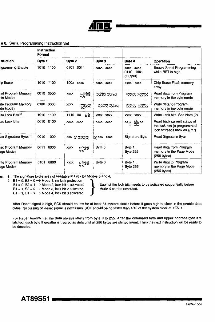
e 8. Serial Programming Instruction Set
Instruction i : Format I
I
i Byte2 I - -~
truction Byte 1 i Byte3 Byte 4 Operation
'gramming Enable 1010 1100 ! 0101 0011 : XXJ()( XXJ()( XXJ()( xxxx I
Enable Serial Programming i 1 I 0110 1001 I while RST is high
! (Output) ---------'"._---,- - -- I ip Erase 1010 1100 100x
~:_ I XXJ()(
xxxx XXJ()( XXJ()( Chip Erase Flash memory array
.. Progmm """"'-t('''" 0000 I Read data from Program I XXJ()( -emu> I ~~~~<~ 1'--<O\O"¢ (f)t\I ..... o
I ::;(!{<{c( 00000000 ~e Mode) I i memory in the byte mode
i ite Program Memory I 0100 0000 1 XXJ()( ..... 00)(0 I I
Write data to Program ~~~~::;c~ ,....<OLOv "'(\,/_0
<:«< l 00000000 memory in the byte mode Ite Mode) I -,-- .~.-~--
I --~-
a:;~ I XXJ()(
--_.-
ite Lock Bits(2) 1010 1100 1110 00 XXJ()( xxxx XXJ()( Write Lock bits. See Note (2). -- ----_.------ -
ad Lock Bits 0010 0100 , XXJ()( xxxx ! xxxx xxxx xx &1 ~mxx Read back current status of I \ ..J ..J..J the lock bits (a programmed I , ,
I I lock bit reads back as a "1 ") ---------- .. ~ .. i ad Signature Bytes(1) i 0010 1000 i xxx 1.0 VC")~.,.... lexxx xxxx Signature Byte Read Signature Byte i ««...: « I...:
~------t----- I I ad Program Memory 0011 0000 I xxxx ..... 00)00 i Byte 0
I. Byte 1 ... Read data from Program 1ge Mode) ! I <:tct:<C
i Byte 255 memory in the Page Mode ,
(256 bytes) i ------"-- I
-ite Program Memory I 0101 0000 xxxx ..... OClCO Byte 0 Byte 1 ... Write data to Program 1ge Mode) i 1
::;:::;:«« I Byte 255 memory in the Page Mode
I
i I ! (256 bytes) I I
!s: 1. The signature bytes are not readable In Lock Bit Modes 3 and 4.
B1 ~ 0, B2 ~ 1 ~ Mode 2, lock bit 1 activated ~ of the lock bits needs to be activated sequentially before 2_ B1 ~ 0, B2 ~ 0 ~ Mode 1, no lock protection }
B1 ~ 1, B2 ~ 0 ~ Mode 3, lock bit 2 activated Mode 4 can be executed. B1 ~ 1, B1 ~ 1 ~ Mode 4, lock bit 3 activated
After Reset signal is high, SCK should be low for at least 64 system clocks before it goes high to clock in the enable data bytes. No pulSing of Reset signal is necessary. SCK should be no faster than 1/16 of the system clock at XTAL 1.
For Page ReadlWrite, the data always starts from byte 0 to 255. After the command byte and upper address byte are latched, each byte thereafter is treated as data until all 256 bytes are shifted in/out. Then the next instruction will be ready to be decoded.
AT89S51 2487 A-1 0/01

AT89S51 ~rial Programming Characteristics
~ure 9. Serial Programming Timing
MOSI --",
SCK
MISO --",
Ibre 9. Serial Programming Characteristics, TA = -40°C to 85°C, Vcc = 4.0 - 5.5V (Unless Otherwise Noted)
'ymbol Parameter Min ! Typ Max : Units
l/teLCL Oscillator Frequency 0 33 MHz -------~
CLCL Oscillator Period 30 ns
SHSL ' SCK Pulse Width High I 8teLCL ns .. I
SLSH ! SCK Pulse Width Low 8teLCL I ns
i MOSI Setup to SCK High I 1--------
OVSH teLCL ns !
I I
--f----~---
-SHOX MOSI Hold after SCK High 2teLCL ! ns
SLiV SCK Low to MISO Valid
I
10 t 16 ! 32 I ns ----~-~---
i I
[ERASE , Chip Erase Instruction Cycle TIme
I
500 I ms ~----~----t I
:swc i Serial Byte Write Cycle Time i 64hcL +400 I iJs
19 A-10101

Isolute Maximum Ratings* ,erating Temperature .................................. -55°C to +125°C
~rage Temperature ......................•.............. -65°C to +150°C
Hage on Any Pin Ih Respect to Ground ..................................... -1. OV to +7. OV
Iximum Operating Voltage ............................................ 6.6V
~ Output Current ...................................................... 15.0 mA
~ Characteristics
'NOTICE: Stresses beyond those listed under "Absolute Maximum Ratings" may cause permanent damage to the device. This is a stress rating only and functional operation of the device at these or any other conditions beyond those indicated in the operational sections of this specification is not implied. Exposure to absolute maximum rating conditions for extended periods may affect device reliability.
i values shown in this table are valid for T A = -40°C to 85°C and Vee = 4.0V to 5 5V, unless otherwise noted.
rmbol : Parameter Condition Min Max Units
-0.5 V : Input Low Voltage (Except EA) -------..... --'-----=--~----.-'----'--'----------l----+----------+---1 _1 Input Low Voltage (EA) I
0.2 Vee-0.1
" Input High VOltage····-·····-t! -(Ex-c-e-pt-xr.-A-l-' ,-R-S-T-) ---.-
~-,--·----ln..:p-u-t-H..::i9'-h-Y,-0-lta-'g--e------+I-'('-XTAL1, RST)
Output Low Voltage(1) (Ports T 1,2,3) i 10L = 1.6 mA
i, Output low Vottage(1) ---·r=----·-------lL1 : (Port 0, ALE, PSEN) I 10L = 3.2 mA ~--'-rl ~-~-·~--~--·-·--r----------
lL
-0.5 0.2 Vee-0.3 V ... -
.j_~~2.~ee+0.9 Vce+0.5 V
I 0.7 Vee Vee+0.5 I V
i 0.45 I V
: - -_ .. _-----_.- ~--.
I 0.45 V
--.. --: 10H = -60 ~A, Vee = 5V ± 10% ...... - .. -.---+-----+----+----1
i 10H = -25 ~A Output High Voltage f-i .::0'.'---..:.....--.----------1---...:::''--+-----+-----1
H (Ports 1,2,3, ALE, PSEN) I 10H = -10 ~A ~---~!--------------+~.~-----------+---~-.~-.--.--
IOH = -800 ~A, Vee = 5V ± 10% !
i I 10H = -300 ~A , Output High Voltage ! H1 I (Port 0 in External Bus Mode) 10H = -80 ~A
~---+_------- .. - . "'-.-.--.-. r·..c------------Logical 0 Input Current (Ports 1,2,3) I VIN =0.45V
~--.. -. _· __ ·_· __ ·_--_· .. _··_·----+1 ~~-... -.-.. --.. I Logical 1 to 0 Transition Current , (Ports 1,2,3) I VIN = 2V, Vee = 5V ± 10% ! Input l~-ak-a-g-e-c··u-r-r-e·n·-t (-Po--rt-O-, -:1--"'---=--------+-----+.-----+----1
EA) : 0.45 < Y'N < Vee f----··--I-·---··---··--···-··-··---~c---........c.c.............=---·-·-·----·-........;-----+----+-----1
"1ST : Reset Pulldown Resistor I i 50 300 K.Q
0. ------~!-PI-·n-Ca-p-a-ci-ta-n-ce---._-_ -_-_-~_-.rl-Te-s-t-F·-r-eq-··-~:-1 MHz, TA = 25°C -1-----.- . ____ ~~ __ ._ ... _p_F_
'I' _.25 mA
i 6.5 mA
Active Mode, 12 MHz 1--------_._._ ... Power Supply Current Idle Mode, 12 MHz ~--~~-~-----+-
Power-down Mode(2) Vee = 5.5V 50
es: 1. Under steady state (non-transient) conditions, 10L must be externally limited as follows: Maximum IOL per port pin: 10 mA Maximum 10L per 8-bit port: Port 0: 26 mA Ports 1, 2, 3: 15 mA Maximum total 10l for all output pins: 71 mA If IOl exceeds the test condition, VOL may exceed the related specification. Pins are not guaranteed to sink current greater than the listed test conditions.
2. Minimum Vee for Power-down is 2V.
AT89S51 2487A-10/01

AT89S51
: Characteristics ler operating conditions, load capacitance for Port 0, ALEIPROG, and PSEN = 100 pF; load capacitance for all other luts = 80 pF.
ternal Program and Data Memory Characteristics 1 12 MHz Oscillator i Variable Oscillator I
f Parameter i Min i Max i Min Max i Units mbol
",CL,:,:C::cL ___ 1-+-0~s_Cillator Frequency ---I-----__j __ ---.---_+! __ ~0 __ _+--~33---+-~~ LL ___ . _IA~E Pulse Width I 127 i 21cLcL-40 -~-i nnss
LL ! Address Valid to ALE Low 43 lcLCL-25 '==--__ -L -----. -------- --+----___l----------+--.:'~=-=---+_----~I-----
AX I Address Hold After ALE Low 48! I tCLCL -25 i ns =---il--------------------+.------+-------+--':"::':"=-----l--------'-------I IV I ALE Low to Valid Instruction In i 233 I 4lcLCL-65 I ns "-----~---------.-~~ .. ----~--------+ II -~---+-----+------+-~----'=------r_-.-~------1
PL I ALE Low to J5SEN Low 43 hCL-25 ' ns
~!'-:=-=J J5SEN Pulse Width 1 205 I 3tcLCL -45 ! J5SEN Low to Valid I nstruction In i 145 3lcLCL -60 !
--·-------___ll------l-------------+------+----""==--~,-----j
"'(IX'---___ -'- 1~~I~_stru~i.?~_~Old_A __ ft~e~r_p~s_E~N ___ _l_i--~0_ ~-"'i _____ -1-___ ° __ -+, _____ ... ;: _~n~s __ i
"C~::_.~._--~-~--~---_--_'_--_-~n-'_:~~~~~~In...:t_:::..t_~-.:.u_d..:.ct_d-'i_:~:~:~~~:...:I_~d..:.A_..:.ft:e_r~p~_s~E~N~~~~_=_-+-II--~_-_-7 __ 5_--_--_-_:iC---------5~9~~~~:~~~lc:::::L-C:L_--8~-=-t-+, ~~lc~_'L'L_C~L'--_2_~5~~._:111-,-------~~:·.~~~ /IV Address to Valid Instruction In 312 i 5hcL-80 ns
I' --- I---------+-----i---==----t----i
10 I 10 ns
ns
.IV ns
i PSEN Low to Address Float
RH : RD Pulse Width I 400 6lcLCL -100 ~----i'--------------j---.-------+----+-~=----_+----_+----i
~Lw"CH'-------1j---W---R-P-ul-se----W----idt--h---------------___ --+ __ 4_0_0_--+ _____ f_ 6lcLCL-1OO __ f- ___________ f--__ ns ____ _
~ ____ ~RD_~0~_:~~~_'lid.:.....:D..:.a...:ta_'l_n ______ +-____ +_--2-5-2-___lI _____ -J--_5lc~LC~L~-90 _ _+--ns-__j I 0 ~
ns
Data Hold After RD --.. --------------------__j------+-----+------__J_-------f-------I
I I
I I 97 i 2lcLcL-28 I
_______ _l_i'--5-1~7--+ii----___l-8lc~L~cL~--15~0-l_i'--n-s-_f i Address to ~d D~I~----------=1___ _ __ +_--58-5---+ li _____ -J--_9lc-=L=c~L-_I65 _ __+:--ns---j
ALE Low to RD or WR Low i 200 I 300 3hcL -50 3lcLCL +50 I ns +---------------!-'-----___l---'=='------J-------=-=-----+---__j
oz Data Float After Ri5 ns
ox -.--~-.. -- ------'T
o
ALE Low to Valid Data In
WL
IiwL Address to RD or WR Low 203 i 4lcLCL-75 I ~=--------------~--~-----I+-----I--------l-~~--I------+-----f
Itov.x _____ .~ .. _Data Valid to W_R"li._ra_n._s_rti_o_n _____ +, __ 2_3 __ +----__ __ +------'lc=-L::::.CL=--.3_0~_ ns .. --- - i 1- -+-1 -- ------+--- ns ---~ ___ ---,_~ilta ~a~_~0_~~_':li~~ __________ -+-__ 4_33 __ _ii-----l__-7lc..::::::Lc::L~-I-30-+--------'f---------1 ,
ns
Data Hold After WR i 33 lcLCL -25 i _____ ---+ __ n_s_~ ~----+ -----...::.:... --+-
o ns .AZ i RD Low to Address Float 0 I t===---+---------~-------- f-----~------__J_----__+-----_+,-----+-----I
i RD or WR High to ALE High 43 123 hCL -25 i lcLcL +25 ns HLH
21 A-10101

:ternal Program Memory Read Cycle
i:==.. tLHLL -
ALE " / "-t"LPH
t AvLL tLUV
-=- t LLPL I-tpLiV
-- +-tplAZ +-tpXAv->'
tLLAX tpXiZ
tpXiX-~ r-PORTO >- AO - A7 INSTRIN J> > I- AO -A7
tAViV
PORT 2 AS - A15 X AS - A15
rternal Data Memory Read Cycle
ALE I:=-tLHLL----------
"--- -tWHLH
t LL"" ~ ~
f4-- tRLRH ---0
~tLLWL--
~tLLAX--iO
...-tAvLL- - tRL"" 1+-+ tRHDZ
tRlAZ --- - ---- :+- f-tRHDX
RD
PORT 0 ::>- AO - A7 FROM RI OR DPl - DATA IN :13 AO - A7 FROM PGl INSTR IN
t AVWL
IAVDV -~
PORT 2 - P2.0 - P2.7 OR AS - A15 FROM DPH AS - A15 FROM PGH
AT89S51 2487A-10101

AT89S51
:ternal Data Memory Write Cycle
ctLHLL--+
ALE - ~ lwHLH
I---- t LLWL tWLWH -
I+--tLLAJ( -----10
+--tAVLL- !avwx - I- - +- tWHQX
I-!aVWH-
PORT 0 =>- AO - A7 FROM RI OR DPl DATA OUT I>( XAO - A7 FROM pel INSTR IN
tAVWL
PORT 2 ---...
P2.0 - P2.7 OR A8 - At5 FROM DPH X AS - At5 FROM PCH
dernal Clock Drive Waveforms
0.45V
hCL
ernal Clock Drive Parameter Min Max Units
: Oscillator Frequency , 0 f==·------..jl-------------------T-----------+--------+--
LeL i Clock Period . 30 I-----~-L-----------------+---------t__--------f__-HCX ! High Time 12 ~9)(===-1-L-O-w-T-im-e---------+----1-2----r_+----.==-_-.-_-_-_-_ -_-+----n-s----i
~n~ I 5 ~
33 MHz
ns
~
LCH
HCL Fall Time 5 ns
23 A-tOIOt

Irial Port Timing: Shift Register Mode Test Conditions
i values in this table are valid for Vcc= 4.0V to 5.5V and Load Capacitance = 80 pF. ,
12 MHzOsc i Variable Oscillator
'mbol Parameter Min I
XL ' Serial Port Clock Cycle Time 1.0
Output Data Setup to Clock Rising Edge l 700 IXH
i O~t~~tD~t~ H~ld Afte~Ck,ck Rising Ed~~--"-J -<ox
<DX Input Data Hold After Clock Rising Edge 1
<DV Clock Rising Edge to Input Data Valid
lift Register Mode Timing Waveforms INSTRUCTION
ALE
CLOCK
,WRITE TO SBUF, • OUTPUT DATA
! CLEAR RI !
... INPUT DATA
Testing Input/Output Waveforms(1)
Vee ·O.5V
O.45V
50
0
0.2 Vee + 0.9V
TEST POINTS
0.2 Vee' O.lV
Max Min Max
12tcLCL , 1OtcLCL-133
'- -------.~-----
2tcLcL-80
0 -I
700 I 1 OtCLCL -133
Units
fJS i
ns
ns
ns
ns
e: 1. AC Inputs during testing are driven at V cc - 0.5V for a logic 1 and 0.45V for a logic O. Timing measurements are made at VIH min. for a logic 1 and VIL max. for a logic O.
at Waveforms(1)
VLOAO
+ O.1V
vLOAD ----(
V LOAD' O.W
e: 1. For timing purposes, a port pin is no longer floating when a 100 mV change from load voltage occurs. A port pin begins to float when a 100 mV change from the loaded VOf-IVOL level occurs.
AT89S51 2487A-10101

AT89S51
dering Information Speed I Power I I
I i ! (MHz) i Supply ! Ordering Code Package Operation Range
24 4.0V to 5.5V I AT89S51-24AC 44A Commercial
I AT89S51-24JC 44J (O°C to 70°C)
I AT89S51-24PC 40P6
AT89S51-24AI I44A
Industrial
ATB9S51-24J1 44J (-40°C to B5 0C)
i AT89S51-24PI 40P6
33 4.5Vto5.5V AT89851-33AC 44A Commercial AT89S51-33JC 44J (O"C to 70"C) AT89851-33PC 4OP6
~ = Preliminary Availability
Package Type
44-lead, Thin Plastic Gull Wing Quad Flatpack (TQFP)
, 44-lead, Plastic J-Ieaded Chip Carrier (PLCC)
I 40-pin, 0.600" Wide, Plastic Duallnline Package (PDIP)
25

Ickaging Information
44A, 44-lead, Thin (1.0 mm) Plastic Gull Wing Quad Flat Package (TQFP) Dimensions in Millimeters and (Inches)'
0.BO(0.031) BSe
, ~___ ' 12.21(0.478} so r ~ 11.75(0,458)
I
0.45(0.018) ';;c: J 0,30(0.0'2)
-!
~--~-1 '0"0(0.394) sa r 9.90(0.386)
! r- ',20(0,047) MAX
g~:~~; -H:~[br-ffil-rr~-UTI-[][1-illll-'Jl-~ , \ ~ I 0.75(0.030) O.1S(O.00fi) j
F 0.45(0.018) 0.05(0.002)
'Controlling dimension: millimeters
40P6, 40-pin, 0.600" Wide, Plastic Duallnline Package (PDIP) Dimensions in Inches and (Millimeters) JEDEC STANDARD MS-011 AC
I 2,07(52,6) I
I
2.04(51.8) PIN 1 i
~\f 0 --1 CJ 0 C' \ \L1D~ __
! 1,1 ,i ! ! t I / / ;' r1 .~~4.4) f ! ! ! :' " !S30(,3:5j' I I : ; : 'l I LC-J \'lTJTrtTTTlJ': '\-o~ --
i -----; l-- .090(2.29) I~ , ,900(48,26) REF -_I ' MAX
220{S.S9) 005( '27) MAX i!' 'MIN
SEpA~~,~ I 0rt Ir~u~;r, f, ~2 ~l,f,~-t ,065(',65)
'6'(409~ '" I ,,- --',"-,-" :-J ",0'5(,38') .125(3.18): ! __ il __ 022(559)
, --- ,065(' ,65) :0'4(:356) .110(2.79) .041(1.04)
:090(2:29) . ,630('6,0) ,
r-- .590(15.of--
ill 1.\\ fs REF 012(.305) --u- --.i\\~ ·b68n~(3)
~ :=~ ~:~i----i
AT89S51
44J, 44-lead, Plastic J-Ieaded Chip Carrier (PLCC) Dimensions in Inches and (Millimeters)
.045(1.14) X 45° PIN NO.1 .045(1.14) X30Q-45~
J ,'DENTIFY
T'--------L_ C '656('6,7)sa
I -,650('6,5)
,032(,8'3) :026(.600) -.1 ~ ,695(' 7]) sa
.685(17.4)
T __ I .050(1.27) TYP -----,-----::-:-.-:-.
_-_ ,500{'2.7) REF sa
'c ,i -c- ,630('6,0)
I ,590('5,0)
,02'(,533) _ ' :0'3(,330)
'cc' ,043{' ,09) -----,020(,508) .120(3.05) ,090(2,29)
.180(4.57) ~165(4.19)
,022(,559) X 45' MAX (3X)
2487A-10/01

:mel Headquarters
'rporate Headquarters ~325 Orchard Parkway 3an Jose, CA 95131 rEL (408) 441-0311 =AX (408) 487-2600
!rope !l.tmel SarL 'loute des Arsenaux 41 ::::asa Postale 80 ::::H-1705 Fribourg Switzerland TEL (41) 26-426-5555 ;: AX (41) 26-426-5500
,ia Il.tmel Asia, Ltd. Room 1219 ::::hinachem Golden Plaza 77 Mody Road Tsimhatsui East Kowloon Hong Kong TEL (852) 2721-9778 FAX (852) 2722-1369
pan Atmel Japan K.K. 9F, Tonetsu Shinkawa Bldg. ~-24-8 Shinkawa
huo-ku, Tokyo 104-0033 apan EL (81) 3-3523-3551 AX (81) 3-3523-7581
mel Corporation 2001.
Atmel Product Operations
Atmel Colorado Springs 1150 E. Cheyenne MIn. Blvd. Colorado Springs, CO 80906 TEL (719) 576-3300 FAX (719) 540-1759
Atmel Grenoble Avenue de Rochepleine BP 123 38521 Saint-Egreve Cedex, France TEL (33) 4-7658-3000 FAX (33) 4-7658-3480
Atme/ Heilbronn Theresienstrasse 2 POB 3535 0-74025 Heilbronn, Germany TEL (49) 71 31 672594 FAX (49) 71 31 6724 23
Atmel Nantes La Chantrerie BP 70602 44306 Nantes Cedex 3, France TEL (33) 0 2 40 18 18 18 FAX (33) 0 2 40 18 19 60
Atme/ Rousset Zone Industrielle 13106 Rousset Cedex, France TEL (33) 4-4253-6000 FAX (33) 4-4253-6001
Atmel Smart Card ICs Scottish Enterprise Technology Park East Kilbride, Scotland G75 OaR TEL (44) 1355-357-000 FAX (44) 1355-242-743
e-mail [email protected]
Web Site http://www.atmel.com
I Corporation makes no warranty for the use of its products, other than those expressly contained in the Company's standard warranty h is detailed in Atmel's Terms and Conditions located on the Company's web site. The Company assumes no responsibility for any errors h may appear in this document, reserves the right to change devices or specifications detailed herein at any time without notice, and does
ake any commitment to update the information contained herein. No licenses to patents or other intellectual property of Atmal are granted e Company in connection with the sale of Atmel products, expressly or by implication. Atmers products are not authorized for use as critical
ponents in life support devices or systems.
EL ® is the registered trademark of Atme!.
-51'" is the registered trademark of Intel Corporation. Terms and product names in this document may be marks of others.
i.QJ Printed on recycled paper.
2487A-10101lxM

LAMPlRANG

L7800AB/AC SERIES
PRECISION 1A REGULATORS
• OUTPUT CURRENT IN EXCESS OF 1 A • OUTPUT VOLTAGES OF 5; 6; 8; 9; 12; 15; 18;
20; 24V • THERMAL OVERLOAD PROTECTION • OUTPUT TRANSITION SOA PROTECTION • 2% OUTPUT VOL TAGE TOLERANCE • GUARANTEED IN EXTENDED
TEMPERATURE RANGE
DESCRIPTION The L7800A series of three-terminal positive regulators is available in TO-220 and D2PAK packages and several fixed output voltages, making it useful in a wide range of applications. These regulators can provide local on-card regulation, eliminating the distribution problems associated with single point regUlation. Each type employs internal current limiting, thermal shut-down and safe area protection, making it essentially indestructible. If adequate heat sinking is provided, they can deliver over 1A output current. Although designed primarily as fixed voltage regulators, these devices can be used with external components to obtain adjustable voltages and currents.
BLOCK DIAGRAM
INPU 1
T
November 1999
STAATIl'IG CIRCUIt
CIJIR£NT GE_lllR
r- REFERENCE --<r-I'OLT.t.GE
50A PIIOIECTlON
ERROR ¥l'l.IFER
THEfINIt. PMlTEClIDN
1
TO-220
SEAlES MSS
ELaENT
..-- t)
o~; PIll 2
-'"
1/17

L7800AB/AC
ABSOLUTE MAXIMUM RATINGS Symbol Parameter Value Unit
Vi DC InputVollage (forVo = Sto 18V) 3S V (forVo = 20,24V) 40 V
10 Output Current Internally limited
Ptot Power Dissipation Internally limited
Top Operating Junction Temperature Range (for L780OAC) o to 1S0 °C (for L7800AB) -40 to 12S °c
Tstg Storage Temperature Range - 6S to 1S0 °c
THERMAL DATA Symbol Parameter 02PAK TO-220 Unit
Rthj-case Thermal Resistance Junction-case Max 3 3 °CfW Rthj-amb Thermal Resistance Junction-ambient Max 62.S SO °C/W
CONNECTION DIAGRAM AND ORDERING NUMBERS (top view)
%11 :f :=: -~ OUTPUT GND P P INPUT ,.... .. - PC1192.0
TO-220 02PAK
Type TO-220 02PAK (') Output Voltage
L780SAB L780SABV L780SABD2T SV L7805AC L780SACV L780SACD2T SV L7806AB L7806ABV L7806ABD2T 6V L7806AC L7806ACV L7806ACD2T 6V L7808AB L7808ABV L7808ABD2T 8V L7808AC L7808ACV L7808ACD2T 8V L7809AB L7809ABV L7809ABD2T 9V L7809AC L7809ACV L7809ACD2T 9V L7812AB L7812ABV L7812ABD2T 12V L7812AC L7812ACV L7812ACD2T 12V L781SAB L781SABV L781SABD2T 15V L781 SAC L7815ACV L781SACD2T l5V L78l8AB L7818ABV l8V L7818AC L7818ACV 18V L7820AB L7820ABV 24V L7820AC L7820ACV 24V L7824AB L7824ABV L7824AC L7824ACV . " -()AVAII.ABLEIN TAPE AND REEL WITH -TR SUFFIX
2117

L7800AB/AC
APPLICATION CIRCUIT
L78XX 2
Vi 3
SCHEMATIC DIAGRAM
~-'n'
3/17

L7800AB/AC
TEST CIRCUITS
Figure 1 : DC Parameter Figure 2 : Load Regulation.
11 L78XX Iz I t
Vi : ii,C. l G..33pI'
Co! 0JfE • ~
•• s-matZ
Figure 3 : Ripple Rejection.
5J4
s-nn
4/17

L7800AB/AC
ELECTRICALCHARACTERlsncs FOR L7805A(Vi = 10V, 10 = 1 A, Tj = 0 to 125 °c (L7805AC), T -40 to 125 °c (L7805AB) nless otherwise specifi d) Ii = U Ie
Symbol Parameter Test Conditions Min. Typ. Max. Unit
Vo Output Voltage Tj = 25°C 4.9 5 5.1 V
Vo Output Vollage 10=5mAt01A Po~15W 4.8 5 5.2 V Vi = 7.5to 20 V
t1Vo* Line Regulation Vi = 7.5to 25 V 10=500mA 7 50 mV Vi=8t012V 10 5 mV Vi = 810 12 V TJ=25°C 2 25 mV Vi = 7.3to 20 V Tj= 250C 7 50 mV
t.Vo• Load Regootion 10=5mAto 1 A 25 100 mV 10 = 5 mAto 1.5A Tj = 25°C 30 100 mV 10 = 250 to 750 mA 8 50 mV
Id Quiescent Current Tj = 25°C 4.3 6 mA 6
t.ld Quiescent Current Charge Vi=8t025V 10=500mA 0.8 mA Vi=7.5t020V lj=25°C 0.8 mA 10=5mAt01 A 0.5 mA
SVR SUPIlY VoRage Rejection Vi = 8to 18 V f= 120 Hz 68 dB 10=500mA
Vd Dropout VoRage 10= 1 A Tj = 25°C 2 V
eN Output Noise VoRage B = 10Hzto 100KHz Tj =25 °c 10 I1VlVo
Ro Output Resistance f = 1KHz 17 mil
Ise Short Circuit Current Vi = 35V Tomb =25 °c 0.2 A
Isep Short Circuit Peack Current Tj = 25°C 2.2 A
t.Vo Output Voltage Drift -1.1 mV/oC
IlT
• Load and line regulation are speCified at constant junction temperaure. Changes in Vo due to heating effects must be taken into account separately. Pulse testing with low duty cycle is used.
5/17

L7800AB/AC
ELECTRICAL CHARACTERISTICS FOR L7806A (Vi = 11V, 10 = 1 A, Tj = 0 to 125 °C (L7806AC), Tj = -40 to 125 °C (L7806AB) unless otherwise specifred)
Symbol Parameter Test Conditions Min. Typ. Max. Unit
V o Output Voltage Tj=25°C 5.88 6 6.12 V
Vo Output Voltage 10=5mAtolA Po$15W 5.76 6 6.24 V Vi = 8.6t021 V
~Vo* Line Regulation Vi = 8.6to 25 V 1o = 500mA 9 60 mV Vi = 9to 13 V 11 60 mV Vi =9to13V Tj=25°C 3 30 mV Vi = 8.3to 21 V Tj = 25 "C 9 60 mV
~Vo* Load ReglJation 10=5mAto 1 A 25 100 mV 10 = 5 mAto 1.5A Tj = 25°C 30 100 mV 10 = 250 to 750 mA 10 50 mV
Id Quiesoent Current Tj=25°C 4.3 6 mA 6
~Id Quiesoent Current Change Vi=9t025V 10= 500mA 0.8 mA Vi = 8.6 to 21 V Tj = 25"C 0.8 mA 10=5mAtolA 0.5 mA
SVR Sup~ Voltage Rejection VI=9to19V f= 120 Hz 65 dB 10=500mA
Vd Dropout Vottage 10 = 1 A Tj = 25°C 2 V
eN Output Noise Voltage B = 10Hzto 100KHz Tj =25 °c 10 JlVNo
Ro Output Resistanoe f = 1KHz 17 mil
Ise Short Circuit Current Vi=35V Tamb = 25°C 0.2 A
Isep Short Circuit Peack Current Tj = 25°C 2.2 A
~Vo Output Voltage Drift -0.8 mV/oC
~T
* Load and line regulation are specified at constant junction temperature. Changes in Vo due to heating effects must be taken into account separately. Pulse testing with low duty cycle is used.
6/17

L7800AB/AC
ELECTRICAL CHARACTERISTICS FOR L7808A(Vi = 14V, 10 = 1 A, Tj = Oto 125°C (L7BOBAC), T - -40 to 125°C (L7BOBAB) unless otherwise specified) '1-
Symbol Parameter Test Conditions Min. Typ. Max. Unit
V o Output Voltage Tj = 25°C 7.84 8 8.16 V
Vo Output Voltage 10=5mAtolA Po:> 15W 7.7 8 8.3 V Vi = 10.6to 23 V
IJ,V 0 * Line Regulation Vi = 10.6 to 25 V 10 =500 rnA 12 80 mV Vi= 1110 17V 15 80 mV Vi= 111017V Tj = 25°C 5 40 mV Vi = 10.4 to 23V Tj = 25°C 12 80 mV
I'>.Vo• Load ReglAation 10 = 5 rnA to 1 A 25 100 mV 10 = 5 rnA to 1.5A Tj = 25°C 30 100 mV 10 = 250 to 750 rnA 10 50 mV
Id Qujescent Current Tj=25°C 4.3 6 rnA 6
!lId Quiescent Current Change Vi=11t025V 1o = 500 rnA 0.8 rnA Vi= 10.6t023V Tj = 25°C 0.8 rnA 10 =5 rnA to 1 A 0.5 rnA
SVR Sup~ Voftage Rejection Vi = 11.5to 21.5 V f=120Hz 62 dB 10=500mA
Vd Dropout Vottage 10= 1 A Tj = 250C 2 V
eN Output Noise Voltage B = 10Hzto 100KHz Tj =25 °C 10 jJ.VIVo
Ro Output Resistance f = 1KHz 18 mil
Ise Short Circuit Current Vi=35V Tamb =2SoC 0.2 A
lscp Short Circuit Peack Current Tj = 2SoC 2.2 A
AVo Output Voltage Drift -0.8 mV/oC
6.T
* Load and line regulation are specified at constant junction temperaure. Changes in Vo due to heating effects must be taken into account separately. Pulse testing with low duty cycle is used.
7/17

L7800AB/AC
ELECTRICAL CHARACTERISTICS FOR L7809A(Vi = 15V, 10 = 1 A, Tj = Oto 125 °c (L7809AC), Tj = -40 to 125 °c (L7809AB) unless otherwise specified)
Symbol Parameter Test Conditions Min. Typ. Max. Unit
Vo Output Voltage Tj = 25°C 8.82 9 9.18 V
Vo Output Voltage 10=5mAt01 A Po ,.;15W 8.65 9 9.35 V Vi = 10.6to 23V
ll.Vo* Line Regulation Vi = 10.610 25 V 10=500 mA 12 90 mV Vi=11t017V 15 90 mV Vi = 11 to 17 V Tj=25°C 5 45 mV Vi = 10.410 23V Tj = 25°C 12 90 mV
/'iVa' Load Regulation 10=5mAto 1 A 25 100 mV 10=5mAto 1.5A Tj = 25°C 30 100 mV 10 = 250 to 750 mA 10 50 mV
Id Quiescent Current Tj=25°C 4.3 6 mA 6
!'lId Quiescent Current Change Vi = 11 to 25 V 1o = 500mA 0.8 mA Vi = 10.6to 23 V Tj = 25°C 0.8 mA 10=5mAt01 A 0.5 mA
SVR Sup!ti Voltage Rejection Vi= 11.5t021.5V f=120Hz 61 dB 10=500mA
Vd Dropout Vokage 10= 1 A Tj = 25°C 2 V
eN Output Noise Voltage B = 10Hzto 100KHz Tj =25 °c 10 v.VIVo
Ro Output Resistance f = 1KHz 18 mil
Ise Short Circuit Current Vi =35V Tamb = 25°C 0.2 A
Iscp Short Circuit Peack Current Tj =25°C 2.2 A
/'iVa Output Voltage Drift -0.8 mVf'lC AT
• Load and line regulation are specified at constant junction temperaurs. Changes In Vo due to heating effects musl be taken into account separately. Pulse testing with low duty cycle is used.
8/17

l7800AB/AC
ELECTRICAL CHARACTERISTICS FOR L7812A(Vi = 19V, 10 = 1 A, Tj = 0 to 125 °c (L7812AC), Tj = -40 to 125 °c (L7812AB) unless otherwise specified)
Symbol Parameter Test Conditions Min. Typ. Max. Unit
Vo Output Voltage Tj = 25°C 11.75 12 12.25 V
Vo Output Voltage 10=5mAt01 A Po,,;15W 11.5 12 12.5 V V; = 14.8to 27V
!1 Yo' Line Regulation Vi = 14.8to 30 V 10 =500 mA 13 120 mV V;=16t022V 16 120 mV Vi = 16t022 V Tj = 25°C 6 60 mV Vi= 14.5t027V Tj = 25°C 13 120 mV
!1Vo' Load RegtJation 10=5mAto 1 A 25 100 mV 10 = 5 mA to 1.5A Tj = 25°C 30 100 mV 10 = 250 to 750 mA 10 50 mV
Id Quiescent Current Tj = 25°C 4.4 6 mA 6
!1ld Quiescent Current Change Vi= 15t030V 10=500mA 0.8 mA Vi = 14.810 27V Tj= 25°C 0.8 mA 10=5mAt01A 0.5 mA
SVR Sup~ Voltage Rejection Vi=15t025V f= 120Hz 60 dB 1o =500 mA
Vd Dropout Voltage 10= 1 A Tj = 25°C 2 V
eN Output Noise Voltage B = 10Hzto 100KHz Tj=25°C 10 iJoVlVo
Ro Output Resistance f = 1KHz 18 mil
Ise Short Circuit Current Vi = 35V Tamb = 25°C 0.2 A
Iscp Short Circuit Peack Current Tj = 25°C 2.2 A
!1Vo Output Voltage Drift -1 mV/oC
!1T
• Load and line regulation are specified at constant junction tempen:ture. Changes in Vo due to heating effects must be taken into aooount separately. Pulse testing with low duty cycle is used.
9/17

L7800AB/AC
ELECTRICAL CHARACTERISTICS FOR L7815A{Vi = 23V.lo = 1 A. Tj = Oto 125 °c (L7815AC). Tj = -40 to 125 °c (L7815AB) unless otherwise specified)
Symbol Parameter Test Conditions Min. Typ. Max. Unit
V o Output Voltage Tj = 25°C 14.7 15 15.3 V
V o Output Voltage 10=5mAto1 A Po,;15W 14.4 15 15.6 V Vi = 17.9to 30V
I'No* Line Reguation Vi = 17.9 to 30V lo=500mA 13 150 mV Vi = 20 to 26 V 16 150 mV Vi = 20 to 26 V Tj = 25°C 6 75 mV Vi = 17.5 to 30V Tj = 25°C 13 150 mV
I'J.Vo* Load Reguation 10=5mAto 1 A 25 100 mV 10 = 5 mAto 1.5A Tj = 25°C 30 100 mV 10 = 250 to 750 mA 10 50 mV
Id Quiescent Current Tj = 25°C 4.4 6 mA 6
I'J.ld Quiescent Current Change Vi= 17.5t030V 10= 500mA 0.8 mA Vi = 17.5to 30V Tj = 25°C 0.8 mA lo=5mAto 1 A 0.5 mA
SVR SuprJy VoHage Re;,ction Vi = 18.5to 28.5 V f = 120 Hz 58 dB 10=500mA
Vd Dropout Vottage 10 = 1 A Tj = 25°C 2 V
eN Output Noise Vottage B = 10Hz to 100KHz Tj =25 °c 10 IlVNo
Ro Output ReSistance f = 1KHz 19 mil
Ise Short Circui1 Current Vi=35V Tamb =25°C 0.2 A
Iscp Short Circuit Peack Cunent T j = 25°C 2.2 A
I'J.Vo Output Voltage Drift -1 mV/oC
t.T
* Load and line regulation are specified at constant junction tempenture. Changes in Vo due to healing effects must be taken into account separately. Pulse testing with low duty cycle is used.
10/17
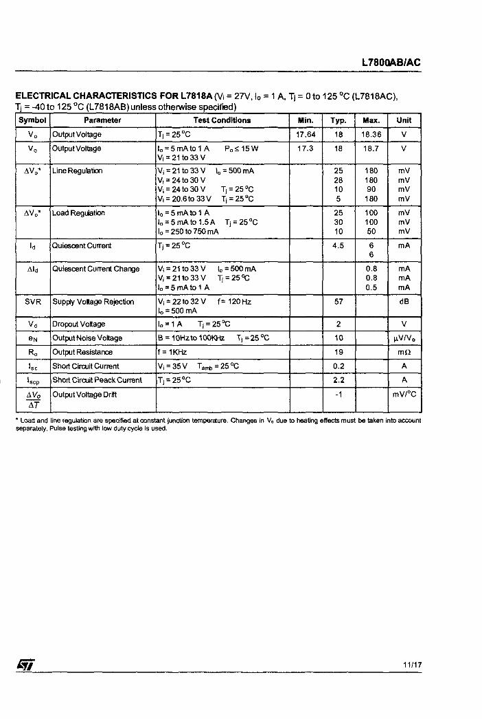
L7800AB/AC
ELECTRICALCHARACTERlsncs FOR L7818A{Vi = 27V, 10 = 1 A, Tj = Oto 125 °c (L7818AC), Tj = -40 to 125 °c (L7818AB) unless otherwise specified)
Symbol Parameter Test Conditions Min. Typ. Max. Unit
Vo Output VoHage Tj=25°C 17.64 18 18.36 V
Vo Output Voltage 10=5mAtolA Po,;;15W 17.3 18 18.7 V Vi = 211033 V
!1Vo' Line Reguation Vi = 21 to 33 V 1o = 500mA 25 180 mV Vi = 24 to 30 V 28 180 mV Vi = 24 to 30 V Tj = 25°C 10 90 mV Vi = 20.6 to 33 V Tj = 25°C 5 180 mV
!1Vo' Load RegtJation 1o =5mAto 1 A 25 100 mV 10 = 5 mA to 1.5A Tj = 25°C 30 100 mV 10 = 250 to 750 mA 10 50 mV
Id Quiescent Current Tj=25°C 4.5 6 mA 6
!1ld Quiescent Current Change Vi = 21 to 33 V 1o = 500mA 0.8 mA Vi = 211033 V Tj = 25"C 0.8 mA 10 =5mAto 1 A 0.5 mA
SVR Sup~ Voltage Rejection Vi=22t032V f= 120 Hz 57 dB 10=5OOmA
Vd Dropout VoKage 10= 1 A Tj = 25°C 2 V
eN Output Noise Voltage B = 10Hzto 100KHz Tj=25°C 10 IlVNo
Ro Output Resistance f = 1KHz 19 mQ
Ise Short Circuit Current Vi=35V Tamb = 25°C 0.2 A
Iscp Short Circuit Peack Current Tj = 25°C 2.2 A
!1Vo Output Voltage Drift -1 mV/oC
!1T
• Load and line regulation are specified at constant junction temperaure. Changes in Vo due 10 heating effects must be taken inlo account separately. Pulse testing with low duty cycle is used.
11/17

L7800AB/AC
ELECTRICAL CHARACTERISTICS FOR L7820A (Vi = 28V. 10 = 1 A. Tj = 0 to 125 °c (L7820AC). Tj = -40 to 125 °c (L 7820AB) unless otherwise specified)
Symbol Parameter Test Conditions Min. Typ. Max. Unit
Vo Output Voltage Tj = 25°C 19.6 20 20.4 V
Vo Output Voltage 10=5 mAto 1 A Po:515W 19.2 20 20.8 V Vi = 23t035 V
AVo' Line RegUBtion Vi = 23t035 V 1o = 500mA 200 mV Vi = 26 to 32 V 200 mV Vi = 26 to 32 V Tj = 25°C 100 mV Vi= 23 to 32 V Tj = 25°C 200 mV
I!..v 0' Load Regootion 10=5mAto 1 A 25 100 mV 10 = 5 mAto 1.5A Tj = 25°C 30 100 mV 10 = 250 to 750 mA 10 50 mV
Id Quiescent Current Tj=25°C 4.5 6 mA 6
t.ld Quiescent Current Change Vi=23t035V 10=500mA 0.8 mA Vi=23t035V Tj = 250C 0.8 mA 10=5mAt01A 0.5 mA
SVR SUPIiY Voltage Rejection Vi = 24 to 35 V f= 120 Hz 56 dB 1o = 500 mA
Vd Dropout Vottage 10 = 1 A Tj = 25°C 2 V
eN Output Noise Voltage B = 10Hzto 100KHz Tj =25 °c 10 tJ.VIVo
Ro Output Resistance f = 1KHz 20 mQ
Ise Short Circuit Current Vi=35V Tomb =25°C 0.2 A
Iscp Short Circuit Peack Current Tj = 25°C 2.2 A
t.Vo Output Voltage Drift -1 mV/oC
IlT
• Load and line regulation are speci~ed at constant junction temper.rure. Changes in Yo due to heating effects must be taken into account separately. Pulse testing with low duty cycle is used.
12117

l780QAB/AC
ELECTRICAL CHARACTERISTICS FOR L7824A (Vi = 33V, 10 = 1 A, Tj = 0 to 125 °c (L 7824AC), Tj = -40 to 125 °c (L7824AB) unless otherwise specified)
Symbol Parameter Test Conditions Min. Typ. Max. Unit
Va Output Voltage Tj=25°C 23.5 24 24.5 V
Va Output Voltage lo=5mAt01 A PoS15W 23 24 25 V Vi = 27.3to 38 V
AVo' Line Reguation Vi=27t038V 10 = 500 rnA 31 240 mV Vi=30t036V 35 240 mV Vi=30t036V Tj = 25°C 14 120 mV Vi = 26.7 to 38V Tj = 25°C 31 240 mV
AVo' Load Reguation lo=5mAt01 A 25 100 mV 10 = 5 rnA to 1.5 A Tj = 25°C 30 100 mV 10 = 250 to 750 rnA 10 50 mV
Id Quiescent Current Tj=25°C 4.6 6 rnA 6
Aid Quiescent Current Change Vi = 27.3 to 38 V 10= 500 mA 0.8 rnA Vi = 27.3to 38V Tj =25°C 0.8 rnA 10=5mAto 1 A 0.5 rnA
SVR Sup~ Voltage Rejection Vi=28t038V f= 120 Hz 54 dB 1o = 500 rnA
Vd Dropout vottage 10 = 1 A Tj = 25°C 2 V
eN Output Noise Voltage B = 10Hzto 100KHz TJ =25 °c 10 IlVNo
Ro Output Resistance f = 1KHz 20 mQ
Ise Short Circuit Current Vi=35V Tamb =25°C 0.2 A
Isep Short Circuit Peack Current Tj = 25°C 2.2 A
AVo Output Voltage Drift -1.5 mV/oC
!!.T
• Load and line regulation are specified at constant junction temperaure. Changes in V, due to heating effects must be taken into account separately. Pulse testing with low duty cycle is used.
13/17

L7800AB/AC
APPLICA nONS INFORMA nON
DESIGN CONSIDERATIONS The L 7800A Series of fixed voltage regulators are designed with Thermal Overload Protection that shuts down the circuit when subjected to an excessive power overload condition, Internal Short-circuit Protection that limits the maximum current the circuit will pass, and Output Transistor Safe-Area Compensation that reduces the output short-circuit current as the voltage across the pass transistor is increased. In many low current applications, compensation capaCitors are not required. However, it is recommended that the regulator input be bypassed with a capacitor if the regulator is
Figure 4 : Current Regulator.
Figure 6 : Current Boost Regulator.
R _ VSEO! 1 I
JREO-~ VSEQ
10 = I REG + Q, (I REG~)
14/17
connected to the power supply filter with long wire lengths, or if the output load capacitance is large. An input bypass capacitor should be selected to provide good high-frequency characteristics to insure stable operation under all load conditions. A O.33f.!F or larger tantalum, mylar, or other capacitor having low internal impedance at high frequencies should be chosen. The bypass capacitor should be mounted with the shortest possible leads directly across the regulators input terminals. Normally good construction techniques should be used to minimize ground loops and lead resistance drops since the regulator has no external sense lead.
Figure 5 : Adjustable Output Regulator.
s· .......
vo. 7.0Vlo 20V v;- Vo ~2.0V
The addition of an operational amplifier allows adjustmentto higher or intermediate values while retaining regulation characteristics. The minimum voltage obtainable with this arrangement is 2.0V greater than the regulator voltage.
Figure 7 : Short·circuit Protection.
.....+-0.0
The circuit of figure 6 can be modified to provide supply protection against short circuit by adding a short-circuit sense resistor, Rsc, and an additional PNP transistor. The current sensing PNP must be able to handle the short-circuit current of the three-terminal regulator. Therefore, a four-ampere plastic power transistor is specified.

L7800AB/AC
[ TO-220 MECHANICAL DATA
DIM. mm inch
MIN. TYP. MAX. MIN. TYP. MAX.
A 4.40 4.60 0.173 0.181
C 1.23 1.32 0.048 0.051
0 2.40 2.72 0.094 0.107
01 1.27 0.050
E 0.49 0.70 0.019 0.027
F 0.61 0.88 0.024 0.034
F1 1.14 1.70 0.044 0.067
F2 1.14 1.70 0.044 0.067
G 4.95 5.15 0.194 0.203
G1 2.4 2.7 0.094 0.106
H2 10.0 10.40 0.393 0.409
L2 16.4 0.645
L4 13.0 14.0 0.511 0.551
L5 2.65 2.95 0.104 0.116
L6 15.25 15.75 0.600 0.620
L7 6.2 6.6 0.244 0.260
L9 3.5 3.93 0.137 0.154
01A. 3.75 3.85 0.147 0.151
"
L2
~
u..
f"" '-.../"
.. ~ ~ ................ E: .. ..... §l N ~ ........ -.......... ..... -...... (!) :I: -
..l.
~ Dia.
.f'\. ...t N
~ u..
L9
L7
L6 L4 PO 11C
15/17

L7800AB/AC
TO-263 (D2PAK) MECHANICAL DATA
mm inch DIM.
MIN. TYP. MAX. MIN. TYP. MAX.
A 4.4 4.6 0.173 0.181
Ai 2.49 2.69 0.098 0.106
B 0.7 0.93 0.027 0.036
B2 1.14 1.7 0.044 0.067
C OA5 0.6 0.017 0.023
C2 1.23 I 1.35 0.048 0.053 I I
! D 8.95 I 9.35 0.352 0.368 I
I E 10 ! 10A 0.393 0.409
G 4.88 5.28 0.192 0.208
L 15 I 15.85 0.590 0.624
l2 1.27 1.4 0.050 0.055
L3 1.4 1.75 0.055 0.068
D --- .... , , \
A I
C ~ DETAIL"A" DETAIL"A"
Al
I ",.,. + B2 B
I
t "1 +-------r- - ---------6 ~ ---------- ------- ~ • '. I
".,.,. I ~
i --L2 L L3 • • P011P6/F
16/17

L7800AB/AC
Information furnished is believed to be accurate and reliable. However, STMicroelectroncs assumes no responsibility forthe consequences of use of such information nor for any infringement of patents or other rights of third parties which may result from its use. No license is granted by implication or otherwise under any paterlt Oi patent itghts of STMicr{,"J61ecITones. Specification mentioned in this publication are S:Uryjo/i tnr::I1~l)gA W!thOllt notice ThLqpilhHcation s!lf)f:'!l"serles 03nfi repl:;tre8- all i(lforrn~tbn previously supplied. STMicroelectronics produr;t~ <:lre not authorized for use as critical components in !ifesupvort devices or systems withoutexpress written approval of STMicroelectronics.
~ e :::: r K>gO is a registered trademark of STMicroeiectronics
'':; 1999 STMicroelectronics - Printed in Italy - All Rights Reserved
STMicroelectronics GROUP OF COMPANiES
Australia ~ Brazil- China - Finland - France - Germany - Hong Kong - India - Italy - Japan- Malaysia - Malta - Morocco Singapore - Spain - Sweden - Switzerland - United Kingdom - U.S.A
http://wWW.slcom
17117

LAMPIRAN-H

~National Semiconductor November 1994
LM79XX Series 3-Terminal Negative Regulators
General Description The LM79XX series of 3-terminal regulators is availabte with fixed output vMages of -SY, -BY, -12Y. and -1SY. These devices need only one external component-a c0mpensation capacitor at the output. The LM79XX series is packaged in the T0-220 power package and is capable of supplying 1.SA of output current.
These regulators employ internal current ~mtting safe area protection and thermal shutdown for protection against virtually all overload conditions.
Low ground pin cuITent of the LM79)()( series allows output voltage to be easily boosted above the preset value with a resistor divider. The low quiescent current drain of
Connection Diagrams TO-220 Package
o o
Front VIew
OUTPUT
INPUT
GROUND
TlfH/7340~14
Order Numbet- LM790SCT, LM7912CT or LM791SCT See NS Package Numbet" T038
these deVices with a spectfied maximum chenge with line and load ensures good regulation in the voltage boosted mode. For applications requiring other voltages, see LM137 data sheet.
Features • Thermal, short circuit and safe area protection
• High ripple rejection
• 1.SA output CUIT""t • 4% tolerance on preset ou\pIJI voltage
Typical Applications FlxedR~or
~ ~;rf 1.. ~~~; ''''''' 11'4 UIfIXXCT OOT OUTPUT
TUH/7340_3
·Aequired if regulator is separated from filter capacitor by more than 3-. For value given, capacitor must be solid tantalum. 25 ~F aluminum electrolytic may be substnuted.
tRequired for stabiHty. For value given, capacnor must be soUd tantalum. 25 fLF aluminum electrolytic may be substi· tuted. Values given may be increased without limit.
For output capacitance in excess of 100 J.l.F, a high current diode from input to output (1N4001. etc.) will protect the regulator from momentary input shorts.
r-3: ..... CD >< >< t.n CD ..,. ;" U)
~ CD ..,. 3 S" !!. z CD
CQ
a i" 11 CD
CQ c iii -o C;;

Absolute Maximum Ratings (Note 1)
tl Military I Aerospace specified devices are required, Input-Output Differential pleese contact the National Semiconductor Seles 010 ~ -5V) 25V OIflce/Dlstrtbulor. lor avollability and specillcations. 010 ~ -12Vand -15V) 30V
Input Voltage Power Dissipation (Note 2) Internally Umned 010 ~ -SV) -25V Operating Junction Temperature Range O"Cto +125'C 010 ~ -12Vand -1SV) -35V
Storage Temperature Range - 65'C to + 15O"C
Lead Temperature (Soldering, 10 sec.) 230'C
Electrical Characteristics Conditions unless otherwise noted: lOUT ~ 500 mA, C,N ~ 2.2 I'F, COUT ~ 1 "F, O"C '" T J '" + 125'C, Power Dissipation'" 1.5W.
Part Number LM790SC
Output Voltage -5V Unlts
Input Voltage (unless othetwls. opecIIIed) -10V
Symbol Parameter Condttlons Min I Typ I Mel<
Va Output Vottage TJ ~ 25'C -4.8 -5.0 -5.2 V 5 mA s: lOUT s: lA, -4.7S -5.25 V P s: 15W (-20 s: V,N s: -7) V
Il.Vo line Regulation T J ~ 25'C, (Note 3) 8 50 mV (-25 s: V,N s: -7) V
2 15 mV (-12 s: V,N s: -8) V
Il.VO Load Regulation T J ~ 2S'C, (Note 3) S mA s: lOUT s: 1.SA 15 100 mV 250 rnA '" lOUT s: 750 rnA 5 50 rnV
10 Ouiescent Current TJ ~ 25'C 1 2 rnA
Il.IO Quiescent Current With Una 0.5 rnA Change (-25 s:V,N s: -7) V
With Load, 5 rnA s: lOUT s: 1 A 0.5 rnA
Vn Output Noise Voltage TA ~ 2S'C.10Hz s: f s: 100Hz 125 I'V
Ripple Rejection f~ 120Hz 54 66 dB (-18 s: V,N s: -8) V
Dropout Voltage TJ ~ 25'C, lOUT ~ 1A 1.1 V
lOMAX Peak Output CUrrent TJ ~ 2S'C 2.2 A
Average Temperature lOUT ~ 5 rnA, 0.4 mV/oC Coefficient of o C s: TJ s: 100"C Output Vottage
Typical Applications (Continued)
Vartable Oulput
-..1.". l R1 * -,..;.,,",
u~; _L!.
T~:'O SOLID -TANTALUM - TAitT ALUM
"'" " , ... , " lM,.XXCT : ""' ounUT
TLIH/7340-2 *Improvas transient response and ripple re)ection. Do not increase beyond 50 I4F.
(Rl + A2) VOllT = VSET ~
Select R2 as fOllOws: LM790SCT 3000 LM7912CT 7500 LM7915CT 1k
2

Electrical Characteristics (Continued) Cond~ion5 unless otherwise noted: lOUT ~ 500 rnA, CIN ~ 2.2 "F, COUT = 1 ~F, COC::::;: TJ ::::;: + 12S"C, Power DiSSipation = 1.5W.
Part Number LM7912C LM7915C
Output Voltage -12V -15V Units
Input Voltage (unl_ otherwise specified) -19V -23V
Symbol Parameter CondItIon. IIIn I Typ I lIax IIln I Typ I Max
Vo OUtput Votlage TJ ~ 2S'C -11.5 -12.0 -12.5 -14.4 -15.0 -15.6 V 5 mA:> lOUT :> lA, -11.4 -12.6 -14.25 -15.75 V P:> 15W (-27:> VIN:> -14.5) (-30 :> VIN :> -17.5) V
AVo Line Regulation T J ~ 25'C, (Note 3) 5 80 5 100 mV (-30:> V,N:> -14.5) (-30:> Y,N:> -17.5) V
3 30 3 50 mV (-22:> V,N:> -16) (-26 S; Y,N S; -20) V
AVo Load Regulation T J ~ 25'C, (Note 3) 5 mA::::;: lOUT::;;; 1.5A 15 200 15 200 rnV 250 mA :> lOUT S; 750 mA 5 75 5 75 mV
10 Quiescent Current TJ ~ 25'C 1.5 3 1.5 3 rnA
Ala Qutescent Current WithUne 0.5 0.5 mA Change (-30 :> V,N:> -14.5) (-30 :>VIN:> -17.5) V
Wrth Load, 5 mA S; lOUT S; 1 A 0.5 0.5 rnA
Vn Output Noise Voltage TA ~ 25'C,10Hz:> f:> 100Hz 300 375 "V Ripple Rejection f ~ 120Hz 54 70 54 70 dB
(-25:> V,N :> -15) (-30 S; Y,N:> -17.5) V
Dropout Voltage TJ ~ 25'C, lOUT ~ lA 1.1 1.1 V
lOMAX Peak Output Current TJ = 25'C 2.2 2.2 A
Average Temperature lOUT ~ SmA, -0.8 -1.0 rnV/,C Coefficient of o C S; TJ S; l00'C Output Votlage
Note 1: Absolute Maximum Ratings indicate limits beyOnd wtVch damage to the device may occur. Operating Ratings indicate conditions for wtliCh the device is intended to bEl fuoctionaJ, but do not guarantee Specific: Performance limits. For guaranteed specifications and test condtions, see the Elecbical Characteristics.
Note 2: Refer to TypiCal Performance CharacteristicS and Design ConsideratiOns for details.
Note 3': Regulation is measured at a constant junction temperature by pulse testing with a low duty cycle. Changes in output vottage due to heating effects must be taken imo aooount.
Typical Applications (Continued)
Dual Trimmed Supply
.,NPUT <>-<M LW"0-5 :OUT +S.OV
GHD 2.0 -.. 01
0.22 ~r=~ 1 k , ,.. , •• 00,
33
cow
33 • 2.2~r=: : 1= 1 ~r _
.. 02 470 • .. , •• 00,
5k
GHD
-INPUT <>-<L;.j L"7905 :OUT -S.OV
TUH/7340-,(
3
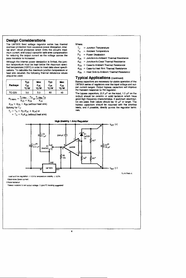
Design Considerations The LM79XX fixed voltage regulator series has thermal overtoad protection from excessive power dissipation, internal short circuit protection which limits the circuit's maximum current, and output transistor safe-area compensation for reducing the output current as the voltage across the pass transistor is increased.
Although the internal power dissipation is limited, the junction temperature must be kept below the maximum specified temperature (125°C) in order to meet data sheet specifications. To calculate the maximum junction temperature or heat sink required. the following thermal resistance values should be used:
Typ Max Package 8JC 8JC
·C/W ·C/W
T0-220 3.0 5.0
PDMAX = TJMax - TAor TJMax TA 8JC + 8CA 8JA
8CA = 8es + 8SA (wtthout heat sink)
Sotving for T J:
TJ = TA + Po (8JC + 8C,.jor
= T A + P08JA (wtthout heat sink)
Typ Max
8JA 8JA ·C/W ·C/W
60 40
Where:
T J = Junction Temperature
T A = Ambient Temperature
PD = Power Dissipation
(} JA = Junction-to-Ambient Thermal Resistance
8JC = Junction-to-Ca88 Thermal Resistance
8GA = Case-to-Ambient Thermal Resistance
8es = Case-to-Heet Sink Thermal Resistance
8SA = Heat Sink·to-Ambient Thermal Resistance
Typical Applications (Continued)
Bypass capamors are necessary for stable operation of the LM79XX senes of regulators over the input voltage and output current ranges. Output bypass capsdtors will improve the transient response by the regulator.
The bypass capacitors, (2.2 "F on the input, 1.0 "F on the output) should be ceramic or $ODd tantalum which have good high frequency characteristics. If aluminum electrolyt· ics are used, their values should be 10 "F or larger. The bypass cepacttors should be mounted with the shortest leads, and n possible, directly across the regulator t"""i· nals.
High Stability 1 Amp Ragulator
= ~~3 ::: 1 "F 200 pf: ~ ';j
7;' f-:l<.:: + = :;Clt ! Q.-t - 2.2 JlF 2N4093 -I"
GHO
I I 'N I Lt.l7905 lOUT
Load and line regulatiOn < 0.01 % temperatul'e stability ,;;; 0.2%
tDetermine Zener current
ttsolid tantalum
R5 'Ok
*Solect resistors to set output voltage. 2 ppmrc tracl<ing suggestad
''-.,;;'
4
/' VOUT (+)
r'Ol
• Lli320 7V
R2'
= ~~2tt :::.0 "
R'! R"
"Ii
TUHI7340-5

Typical Applications (Continued)
5V 'IOUT = 1 mA + A1
2.2 p.f SOLID
TANTALUM
INPUT
-~ ... I t t _.
R"
Ug/lt Controller Using SH\COn Photo Cell
, , , etl...J.!.
25.ur-r , ,
'Lamp brigfltness increase until ~ = io (;:; 1 rnA) + SVlR1.
tNeceSS8l)l only if raw supply filter capacitor is more than 2" from LM7905CT
5
0.1 JAr
TUHI7340-7
5V - tSV etJLB 1.15. WAX TURN-oN CURRENT
TLIH17340-8

Typical Applications (Conbnued)
I I I
CIt ...J.!. 25 ~F"'T"
I I I I
Hlgh-SensltIYtty Ugh, Controlle<
OUT
8V- 15V auLB 1.75A t4AX TURN-ON CURRENT
TlfHI7340-9
"lamp brightness increases until ~ = 5V/Rl (I; can be set as low as 1 !LA) 1~ orWj if fll'H ~ titter capac:OO!' is more. than 2" from lM7905
± lSV, 1 Amp Tracking RegulatOrs
I I I I I I I .. -.::.
~F ...... I
C. 25
I I I I I
: 5" ..!:.
INI
I
U43-40T lOUT
-15 I
GNO
......-25 ~i = ~ r
., R2 50
7 2 -
lW307
• 'l"~
c~ :: ~ 25.uF
"
Vour (+) 15V
R<' 10k
'" ~ 01
R5' • IN -4001 10k 1%
CO .... ON
-'" 02 C 25 ~F ...... " 5k "'---< • ~ IN 4001
I I I I
OUTPUT TRIW
GNO TO -15.0V
J l 'NL lW7915CT lOUT
(-15) (+15) load Regulation at 6.ll = 1A 40 mV 2 mV Output Ripple, CtN = 3000 "F, II = 1"'- 100 ,,\Inns 100 "V~ Temperature Slabitlty 50 mV 50 mV Output Noise 10 Hz :<>: f :;;: 10 kHz 150 p,Vrms 150 JoLvrms
·Resistor tolerance of R4 and AS determine matching of (+) and (-) outputs .
• 0Necessaty only if raw supply fi/l8r c::apacitors are rTlO(S than 3" from regulators.
6
VOUT (-) 15V
ntHI7340-1

Schematic Diagrams
II
G; I
7
> a: ~N ....
• >

en () ':r III 3 I» --12Vand -15V n-O iii"
-=- IQ ... I»
RI8 ~R19 3 4k 5k III
~ 01 .... 02 ~ R6
QO
2 H ~
R' I,.. Al1
~I ~Q' n, You'
DJ 6.tv
!" I n.f=1 fl rO" fi'"l L
R4 ZOk r A8 RI
Rl ~R2 t 20k 20k 1 I ,k .e fRl' '50 1k 6k 0.2
V,N
TUHf73o«1-13

Physical Dimensions incheS (millimeters)
_ 0.2"-0.2'0 _o.330-0.350 ~ ~ [6.10-'.60) [8.38-.... )
O. '00-0.'20 _ __ 0."9-0.153 [2.,.-3.05) /" [3.78-3.89)
r- ~ . _ _ ~ I, -EZ ~ - 0,090-0.110 0.'00 :D.D" . r-:::~:=:::=:==:::::::~ [2.29-2.79) D.'" ------I- r:..: - - ---. I t [10.16~~·~] I I ~ t L pt- - -
/ L-J 0.130-0.160 TIP PIN ., 10 --1 {3.30-4.06]
1.005-1.035 [25.53-26.29)
0.(1;48-0.055 J [1.22-1.40]
TIP
0.027-0.037 _ [0 .• 9-0.9.)
TIP
f 0.190-0.210
[U3~5.33)
0.175-0.185 I
1011- 70 .A r-- ( 0.525-0.555 ) -..j 10.015 :!::; [0.38 :::i:] I / \, [13.34-14.10) I J
[4045-4.70) ..L r 'I: . L 0,0048-0.052 rT :j o
o-'.--J [1.22-1.32)
TAPERED SIDES 1°
LIFE SUPPORT POLICY
T0-220 Outline Pa<:kage IT) Order Nu_ LII7905CT, LM7912CT or LM7915CT
NS Packege Number T03B
T038 (11£'1 t)
NATIONAL'S PRODUCTS ARE NOT AUTHORIZED FOR USE AS CRITICAL COMPONENTS IN LIFE SUPPORT DEVICES OR SYSTEMS WITHOUT THE EXPRESS WRITTEN APPROVAL OF THE PRESIDENT OF NATIONAL SEMICONDUCTOR CORPORATION. As used herein:
1. Ufe support devices or systems are devices or systems wt\ich, (a) are intended for surgal implant into the body, or (b) support or sustain life, and whose failure to perform, when property used in accordance with instructions for use provided in the labeting, can be reasonably expected to result in a significant injury to the user.
2. A critical oomponent is any oornponent of a life support device or system whose failure to perform can be reasonably expected to cause the failure of the life supPOrt device or system, or to affect its safety or effectiveness.
NatIonoISoml_ ~ 1111 west Bardin Road Ariington, TX 76017 Tel: 1(800) 272·9959 FfOC 1(800) 737·7018
-E..-Fax: (+49) 0-1ac..530 85 86
Email: cnjwge_tevm2.nsc.com Ileut8Ch Tel: (H9) 0-180-S30 85 85 English Tel: (+"9) 0-180-532 78 32 Frarw;ais T iii: l H9) 0-180-532 93 58 ItaWIo Tel: (H9) o..1~ 1680
-_ .. Hong Kant Ud. 13th Floor, Strsight Block, Ocean Genb1I, 5 canton Ad. T simshatsui, Kowloon --Tet (852) 2731-1600 Fax: (852) 2736-9980
-_Ltd. Tel: 81-043-29$-2309 Fax: 81~2408

BIODATA
Nama : Agustinus Wijaya
NRP : 5103000043
Tempat, Tgl. Lahir : Iember, 17-08-1981
Agama : Katolik
Telepon : 081-330-226-999
E-mail : Bemad_sienyl808
@yahoo.com
Alamat Rumah : II. Raya Kawi 50
Ienggawah - Jember
Riwayat Pendidikan :
• Tahun 1994 Lulus SDK Maria Fatima III Iember
• Tahun 1997 Lulus SMPK Santa Maria Iember
• Tahun 2000 Lulus SMUK Santo Paulus lember
• Tahun 2005 Lulus Universitas Katolik Widya Mandala Surabaya
r PERPUSTAKAAN\ , Unjvers~ta~ _hilt,) h. ~ c. " .. auda!a :\
I S U .'. ,c.. , '. ------- -