ild2111 digital dc/dc buck controller ic - farnell.com · ptc temperature control current control...
TRANSCRIPT

Power Management & Mult imarket
Datasheet Revision 1.0, 2015-04-08
ILD2111
Digital DC/DC Buck Controller IC

ILD2111
Datasheet 2 Revision 1.0, 2015-04-08
Digital DC/DC Controller with I-Set
Product highlights
Assumes control of functionality where a microcontroller is required in conventional systems
Device configurable by a comprehensive parameter set
High efficiency over wide input and output ranges
High accuracy of +/-5% over output current range and useful temperature
Features
Hysteretic current regulation
Output current adjustable in up to 16 steps with a dynamic range of 1:4 between min. and max. configurable by an external resistor
Flicker-free and phase-aligned PWM dimming based on input PWM signal
Fully configurable internal and external smart overtemperature protection
Open/short load protection
Overpower protection
Applications LED drivers, e.g. 2-stage professional lighting
systems
Integrated electronic control gear for LED luminaires
Description
The ILD2111 is a high-performance microcontroller-based digital DC/DC buck LED controller, designed as a constant current source. The driving current is adjustable with a simple external resistor. Flicker-free dimming supported by means of phase-aligned PWM LED current. An ASSP digital microcontroller-based engine is highly configurable using a comprehensive parameter set to provide fine tuning of operation and protection features. High-precision hysteretic output current regulation is achieved thanks to the digital control loops.
Figure 1. Typical Application
Product type Package
ILD2111 PG-DSO-8-58
VDDP
ILD2111VCC
GD0
PTC
Temperature
Control
Current
Control
VIN
CS
REF/SC
TS
PWM
GND
LEDs5
1
2
3
4
6
7
8
Line Voltage
Rext
MOSFET
BSP373
L6327
PFC+Flyback
DC/DC Buck
GND
UART Interface
Configuration &
In-Circuit Calibration
PWM - Dimming
ZD2V7
External
PWM Signal
PG-DSO-8-58

ILD2111
Table of Contents
Datasheet 3 Revision 1.0, 2015-04-08
Table of Contents
1 Pin Configuration and Description ................................................................................................... 4
2 Block Diagram .................................................................................................................................... 5
3 Functional Description ...................................................................................................................... 6 3.1 Introduction ........................................................................................................................................... 6 3.2 Main Supply (VCC)............................................................................................................................. 11 3.3 Controller Features............................................................................................................................. 11 3.3.1 Configurable Leading Edge Blanking (LEB) and Sampling Time at Pin CS ...................................... 12 3.3.2 Configurable Gate Driver Output ........................................................................................................ 12 3.3.3 Reference Current Setup ................................................................................................................... 13 3.3.4 Output Current Control and Measuring .............................................................................................. 17 3.3.5 Current Startup, Soft-Start and Shutdown Control ............................................................................. 19 3.4 Current Ripple vs. Switching Frequency Control Scheme ................................................................. 20 3.4.1 Fixed Current Ripple .......................................................................................................................... 20 3.4.2 Frequency and Ripple Control ........................................................................................................... 21 3.5 Input Voltage Measurement and Calibration ...................................................................................... 28 3.6 Protection Features ............................................................................................................................ 30 3.6.1 Undervoltage Protection for DC Input Line – VIN Undervoltage ......................................................... 32 3.6.2 Overvoltage Protection for DC Input Line – VIN Overvoltage ............................................................. 32 3.6.3 Output Undervoltage Protection – VOUT Undervoltage ....................................................................... 32 3.6.4 Open Output Protection ..................................................................................................................... 32 3.6.5 Output Overvoltage Protection – VOUT Overvoltage ........................................................................... 33 3.6.6 Output Overpower Protection – POUT Overpower .............................................................................. 33 3.6.7 Overtemperature Protection ............................................................................................................... 34 3.6.8 Overcurrent Protection – Level 2 (OCP2) .......................................................................................... 39 3.6.9 Functional Protections ........................................................................................................................ 39 3.7 External PWM Dimming ..................................................................................................................... 40 3.8 Output Current PWM Modulation ....................................................................................................... 41 3.9 Configuration ...................................................................................................................................... 42 3.9.1 Overview of Configurable Parameters ............................................................................................... 42 3.9.2 Configuration Procedure – Parameter Handling ................................................................................ 52
4 Electrical Characteristics ................................................................................................................ 54 4.1 Definitions ........................................................................................................................................... 54 4.2 Absolute Maximum Ratings ............................................................................................................... 55 4.3 Package Characteristics .................................................................................................................... 56 4.4 Operating Conditions ......................................................................................................................... 56 4.5 DC Electrical Characteristics .............................................................................................................. 57
5 Outline Dimensions ......................................................................................................................... 63

ILD2111
Pin Configuration and Description
Datasheet 4 Revision 1.0, 2015-04-08
1 Pin Configuration and Description
The pin configuration is shown in Figure 2 and Table 1-1. The pin functions are described later.
Figure 2. Pin Configuration Table 1-1. Pin Definitions and Functions
Symbol Pin Type Function
TS 1 I Temperature Sensor The pin TS is used for external temperature measurement using PTC or an appropriate passive temperature sensor.
REF/SC 2 IO Reference/Serial Communication
The pin REF/SC is multiplexed. During startup it is used for reference current sensing by means of an external RC circuit. Afterwards, it serves as a UART serial communication interface.
CS 3 I Current Sense Current measurement on an external shunt resistor.
GD0 4 O Gate Driver Output 0 Output for directly driving a power MOS.
VIN 5 I Voltage Input Voltage input measurement. Requires an external series resistor for voltage sensing and current limitation.
PWM 6 I PWM Dimming Signal Input for PWM-based dimming signal.
VCC 7 I Positive Voltage Supply
IC power supply.
GND 8 O Power and Signal Ground
TS
REF/SC
CS PWM
GND
VCC
GD0 VIN
PG-DSO-8-58 (150mil)
1
2
3
4
8
7
6
5
ILD2111
Block Diagram
Datasheet 5 Revision 1.0, 2015-04-08
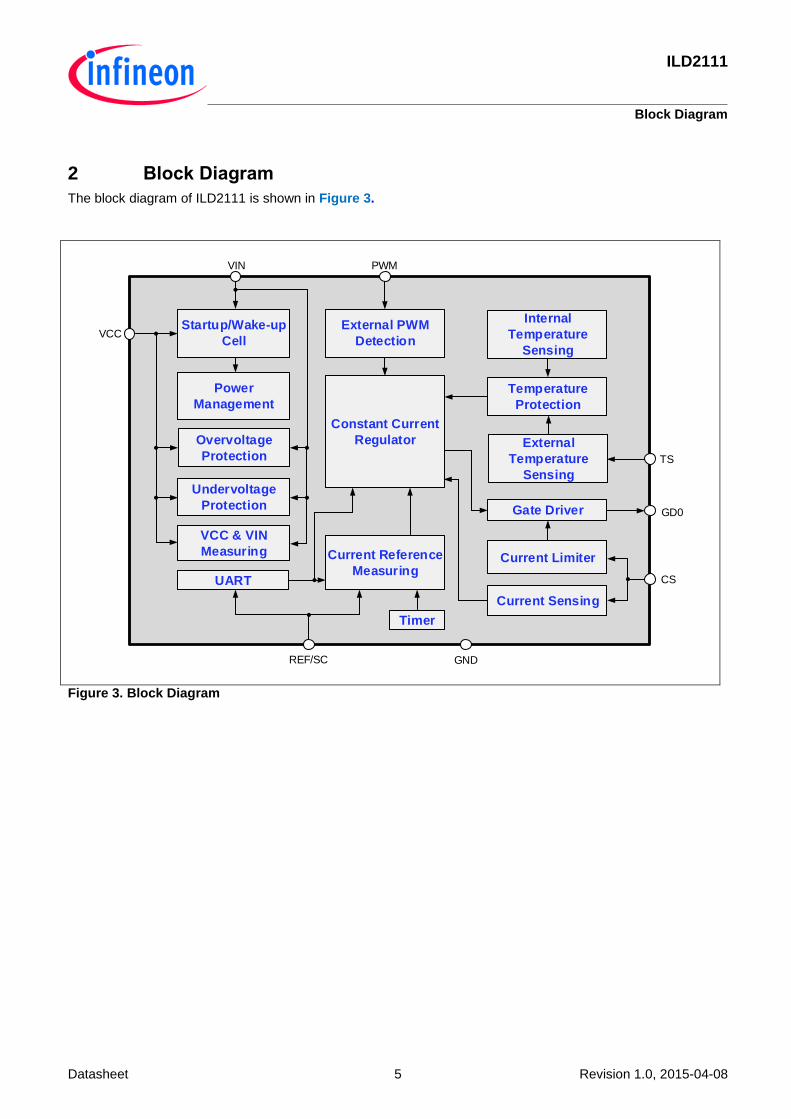
2 Block Diagram
The block diagram of ILD2111 is shown in Figure 3.
Current Reference
Measuring
REF/SC
VIN
VCC
PWM
UART
GND
Constant Current
RegulatorOvervoltage
Protection
Undervoltage
Protection
Startup/Wake-up
Cell
Power
Management
External PWM
Detection
Timer
VCC & VIN
Measuring
TS
GD0
CS
Temperature
Protection
Gate Driver
Current Limiter
Current Sensing
Internal
Temperature
Sensing
External
Temperature
Sensing
Figure 3. Block Diagram

ILD2111
Functional Description
Datasheet 6 Revision 1.0, 2015-04-08
3 Functional Description
The functional description provides an overview of the integrated functions and features, and their relationship. The parameters and equations provided are based on typical values at TA = 25°C. The corresponding minimum and maximum values are shown in Section 4, Electrical Characteristics.
3.1 Introduction
The ILD2111 is a high-performance digital microcontroller-based DC/DC buck LED controller designed as a constant current source with hysteretic output current regulation. The controller typically uses a floating buck topology operating in a Continuous Conduction Mode (CCM). In order to reduce switching losses and increase efficiency, as well as to control the switching frequency over a wide variety of external component values, input voltage and load variations, a frequency ripple control is introduced. Both internal and external temperature measurements are implemented and accompanied with an intelligent temperature protection algorithm with two threshold values. The controller utilizes a variety of protection features, including overpower, open and short load conditions. The ILD2111 is a dimmable device controlled by an external PWM signal. The device can be parameterized by means of a single pin UART interface at the REF/SC pin (see Section 3.9). A complete top-level device operation process, including protection and error handling, is shown in Figure 4. Table 3-1 shows device operating statuses, buck statuses associated with the buck state machine, as well as error and associated error codes. The buck state machine diagram is shown in Figure 5.

ILD2111
Functional Description
Datasheet 7 Revision 1.0, 2015-04-08
Power-upreset
Hardware initialization
Applying parameter patches
Temperature protectioninitialization
ParametersCRC?
YES
NO
Reference current set
UART initialization
VIN_MIN_START
< VIN <VIN_MAX_START
NO
T>T_critical
Buck operation initializationand START
4
1
2
Startup delay
Process UART communication
NO
YES
YES
Parameters Consistency?
YES
NO1
3
T_hot< T <
T_critical
NO
YES
Set internal PWM duty to parameter value
7
8
OPER_STATUS = OPER_ERRERR_STATUS = ERR_PARAM_EMPTY
OPER_STATUS = OPER_ERRERR_STATUS = ERR_PARAM_DATA
OPER_STATUS = OPER_OFFERR_STATUS = ERR_NONE
BUCK_CONTROL = BUCK_OFF
OPER_STATUS = OPER_STARTUPbuck_oper_loop_delay for error restart phases:Delay = 0 – for first start, after HOT and COLD restart and after input undervoltage error.Delay = ERR_RESTART_TIME – after following errors: output undervoltage, output overvoltage, output overpower, open output and input overvoltage
BUCK_CONTROL = BUCK_STARTUPERR_STATUS = ERR_INPUV or ERR_INPOV
ERR_STATUS = ERR_OTI or ERR_OTE
Parameters:ITP_STARTUP_PWM_HOT orETP_STARTUP_PWM_HOT
OPER_STATUS = OPER_RUNBUCK_CONTROL = BUCK_SOFTSTART
Copy OTP to RAM with CRC check and start FW
Copy default parameters from OTP to RAM
Executed from ROM code

ILD2111
Functional Description
Datasheet 8 Revision 1.0, 2015-04-08
Process UART communication
4
VIN_MIN_OPER
< VIN <VIN_MAX_OPER
NO
Process EPWM measurement
Open output?
Process Buck state machine
OCP2 level?
NO
NO
YES
YES
YES
Average check?NO
4
YES
Apply delay (event_counter) Delay(1) = 100 µs Delay(2) = 500 µs Delay(3) = 2500 µs Delay(4+) = OCP2_RESTART_DELAY
Restart hardware PWM engine
VOUT_MIN
< VOUT <VOUT_MAX
NO
Process temperature dimming
POUT < POUT_MAX_LC or POUT_MAX_HC
T > T_critical
NO
NO
YES
Process Calculations and Compensations
5
YES
YES
6
6
6
6
6
OPER_STATUS = OPER_ERRERR_STATUS = ERR_INPUV or ERR_INPOV
OPER_STATUS = OPER_ERRERR_STATUS = ERR_OPEN
One averaging interval is 16 Buck PWM switching cycles
OPER_STATUS = OPER_ERRERR_STATUS = ERR_OUTUV or ERR_OUTOV
OPER_STATUS = OPER_ERRERR_STATUS = ERR_PWR
OPER_STATUS = OPER_ERRERR_STATUS = ERR_OTI or ERR_OTE

ILD2111
Functional Description
Datasheet 9 Revision 1.0, 2015-04-08
Process FRC - Frequency Ripple Controller
Is FRCin steady-state?
Change FRC update interval to lower rate = 16·TPWM·
FRC_REG_INTERVAL_OPER(typically in a range of couple of
seconds)
UART initialization
1
2
NO
YES
4
Hot restart?
Cold restart?
NO
NO1
3YES
YES
FRC update interval
elapsed?
NO
5
YES
Open o
utp
ut e
rror
All o
ther e
rrors
6
7 8
FRC update interval is set to higher rate during startup
Process Buck Shutdown
Figure 4. Device Operating Flowchart
ILD2111
Functional Description
Datasheet 10 Revision 1.0, 2015-04-08
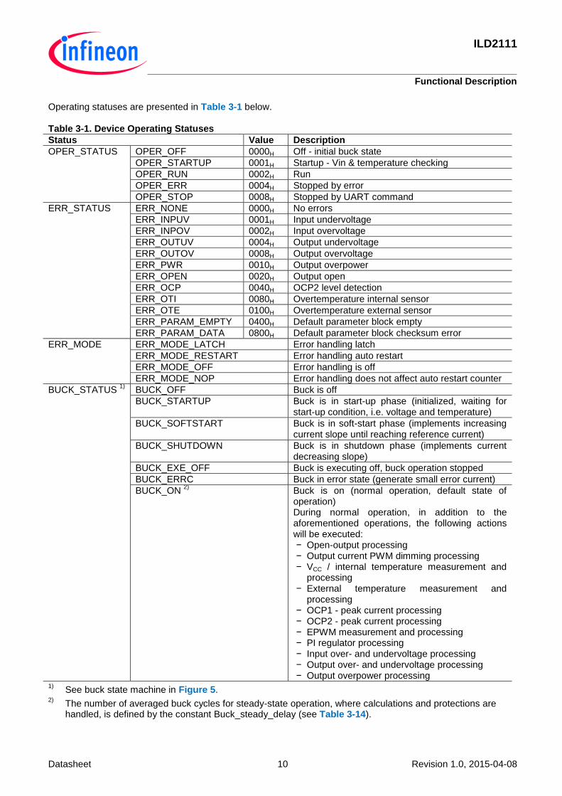
Operating statuses are presented in Table 3-1 below. Table 3-1. Device Operating Statuses
Status Value Description
OPER_STATUS OPER_OFF 0000H Off - initial buck state
OPER_STARTUP 0001H Startup - Vin & temperature checking
OPER_RUN 0002H Run
OPER_ERR 0004H Stopped by error
OPER_STOP 0008H Stopped by UART command
ERR_STATUS ERR_NONE 0000H No errors
ERR_INPUV 0001H Input undervoltage
ERR_INPOV 0002H Input overvoltage
ERR_OUTUV 0004H Output undervoltage
ERR_OUTOV 0008H Output overvoltage
ERR_PWR 0010H Output overpower
ERR_OPEN 0020H Output open
ERR_OCP 0040H OCP2 level detection
ERR_OTI 0080H Overtemperature internal sensor
ERR_OTE 0100H Overtemperature external sensor
ERR_PARAM_EMPTY 0400H Default parameter block empty
ERR_PARAM_DATA 0800H Default parameter block checksum error
ERR_MODE ERR_MODE_LATCH Error handling latch
ERR_MODE_RESTART Error handling auto restart
ERR_MODE_OFF Error handling is off
ERR_MODE_NOP Error handling does not affect auto restart counter
BUCK_STATUS 1)
BUCK_OFF Buck is off
BUCK_STARTUP Buck is in start-up phase (initialized, waiting for start-up condition, i.e. voltage and temperature)
BUCK_SOFTSTART Buck is in soft-start phase (implements increasing current slope until reaching reference current)
BUCK_SHUTDOWN Buck is in shutdown phase (implements current decreasing slope)
BUCK_EXE_OFF Buck is executing off, buck operation stopped
BUCK_ERRC Buck in error state (generate small error current)
BUCK_ON 2)
Buck is on (normal operation, default state of operation) During normal operation, in addition to the aforementioned operations, the following actions will be executed: − Open-output processing − Output current PWM dimming processing − VCC / internal temperature measurement and
processing − External temperature measurement and
processing − OCP1 - peak current processing − OCP2 - peak current processing − EPWM measurement and processing − PI regulator processing − Input over- and undervoltage processing − Output over- and undervoltage processing − Output overpower processing
1) See buck state machine in Figure 5.
2) The number of averaged buck cycles for steady-state operation, where calculations and protections are
handled, is defined by the constant Buck_steady_delay (see Table 3-14).

ILD2111
Functional Description
Datasheet 11 Revision 1.0, 2015-04-08
BUCK_ON
BUCK_STARTUP
BUCK_SOFTSTART
BUCK_SHUTDOWN
BUCK_EXE_OFF
BUCK_ERRC
BUCK_OFF
OPER_OFF
OPER_STARTUP
OPER_RUN
OPER_ERR
START
Figure 5. Buck State Machine
3.2 Main Supply (VCC)
The device is powered via the VCC pin. All device supply voltages are internally generated from the VCC voltage.
3.3 Controller Features
Table 3-2 gives an overview of the controller features that are described in the referenced sections.
Table 3-2. Controller Features
Configurable Leading Edge Blanking (LEB) and Sample Time at Pin CS Section 3.3.1
Configurable Gate Driver Output Section 3.3.2
Reference Current Setup Section 3.3.3
Output Current Control and Measuring Section 3.3.4
Current Startup, Soft-Start and Shutdown Control Section 3.3.5

ILD2111
Functional Description
Datasheet 12 Revision 1.0, 2015-04-08
3.3.1 Configurable Leading Edge Blanking (LEB) and Sampling Time at Pin CS
A configurable leading edge blanking time tCSLEB is integrated into the current sensing path to provide more accurate output current sensing and regulation. Leading-edge spikes during the PowerMOS switch-on phase, as shown in Figure 6, can affect sampled output current values, resulting in imprecise current sensing. The LEB time is used to prevent false overcurrent detection, while the sample time defines the moment of the current sampling for A/D conversion. The time tCSLEB and the sampling time are configured by the constants CS_blanking_time and CS_sample_time respectively (see Table 3-19) in order to provide output current sampling at the moment when no spikes are present.
CSS & H
GD0
TON TOFFtCSLEB tCSLEB
ILD2111
R_current_sense
Figure 6. Configurable Leading Edge Blanking Time at Pin CS
3.3.2 Configurable Gate Driver Output
The gate driver output (GD0) can be configured with respect to the final voltage level and gate drive current, which influence the rising voltage slope for switching on the external PowerMOS (see Figure 7) and therefore a switch-on time. A compromise should and could be made between switching power losses and electromagnetic radiation by using these parameters (especially gate drive current values). The output gate voltage VGDH and gate current IGD can be programmed by the parameters, providing an adjustable PowerMOS turn-on time. The programmable output gate voltage range is from 4.5 V to 15 V (see Table 3-8). VGDH cannot be higher than the power supply voltage VCC, regardless of the programmed value. The programmable gate current range is from 30 mA to 118 mA (see Table 3-8). Figure 7 shows the gate driver output voltage signal. Different rising slopes correspond to different gate driving currents. The slope is proportional to the current.
t
VGD
VGDH
IGD1 < IGD2 < IGD3 < IGD4
IGD1
IGD2
IGD3
IGD4
Figure 7. Configurable Gate Driver Output

ILD2111
Functional Description
Datasheet 13 Revision 1.0, 2015-04-08
3.3.3 Reference Current Setup
The reference current value is obtained by measurement using the value of the external resistor R_iset connected to the pin ‘REF/SC’ together with the reference capacitor C_ref via the discharge time of the capacitor (see Figure 8 and Figure 9). Depending on the resistance of R_iset, the appropriate reference current, stored in a table of 16 currents (see Table 3-12), is used as a reference for the output current. The reference current setup procedure (I-set) will always be executed during the startup sequence or during Open output protection recovery – see Section 3.6.4.
When the internal switch SW is turned on for a short period of time defined by the constant RC_cap_charge_time (see Table 3-19) while the digital output is high, the C_ref is fully charged to Vcref, where this voltage depends on the internal VDDP voltage and voltage divider R_ref_sc – R_iset. R_ref_sc is used for decoupling the reference current measurement circuitry and serial UART communication. Care must be taken that the ratio of R_iset to R_ref_sc is sufficient to have only a low impact on Vcref. Otherwise, it has to be included in the time thresholds calculation. When the switch is turned off, the C_ref discharges through the external resistor R_iset. The discharging time of the capacitor C_ref depends on the value of the external resistor. During the discharging interval, the pin voltage is measured by ADC while an internal timer measures the discharging time. When the capacitor voltage drops below the constant threshold level V_adc_th (constant V_ADC_th, see Table 3-13), the internal timer value is latched and used to determine the reference current from the predefined I-set table.
VDDP= 3.3 V
Software
ControlSW
C_ref R_iset
ADC
REF / SCR_ref_sc
V_ref_rc_charge Vcref
+
UARTInterface
ILD2111
C_filt
Figure 8. Charging and Discharging of the C_ref Capacitance Depending on the Switch State C_filt is a ceramic capacitor used to filter noise, caused by the converter switching operation. Mainly it is used to suppress noise for ADC measurement as well as UART communication.

ILD2111
Functional Description
Datasheet 14 Revision 1.0, 2015-04-08
V_adc_th
tdischarge
ttimeout
t
vADC(t)
Vcref
V_ref_rc_charge = 3.3V
Figure 9. C_ref Discharging Interval Determined by the Reference Resistor Value The charging voltage Vcref is calculated as:
𝑉𝑐𝑟𝑒𝑓 =𝑅_𝑖𝑠𝑒𝑡
𝑅_𝑖𝑠𝑒𝑡+𝑅_𝑟𝑒𝑓_𝑠𝑐∙ 𝑉_𝑟𝑒𝑓_𝑟𝑐_𝑐ℎ𝑎𝑟𝑔𝑒. (1)
The equation for V_adc_th is:
𝑉_𝑎𝑑𝑐_𝑡ℎ = 𝑉𝑐𝑟𝑒𝑓 ∙ 𝑒−
𝑡𝑑𝑖𝑠𝑐ℎ𝑎𝑟𝑔𝑒
𝑅_𝑖𝑠𝑒𝑡∙𝐶_𝑟𝑒𝑓. (2)
Therefore:
𝑡𝑑𝑖𝑠𝑐ℎ𝑎𝑟𝑔𝑒 = 𝑅_𝑖𝑠𝑒𝑡 ∙ 𝐶_𝑟𝑒𝑓 ∙ 𝑙𝑛𝑉𝑐𝑟𝑒𝑓
𝑉_𝑎𝑑𝑐_𝑡ℎ. (3)
If a lower voltage threshold is not reached after the predefined time-out period ttimeout (constant RC_measurement_timeout, see Table 3-19), the reference current determination process ends and the last value from the current table is taken as the reference (Ref_current_16, see Table 3-12). Component values and their tolerances must provide unique thresholds in order to be detected appropriately (see Figure 10).
More accurate equations will be obtained if typical component tolerance values are included.
The following are assumed:
Maximum reference resistance: R_iset_max(n) = R_iset(n) + R_iset_tolerance1
Minimum reference resistance: R_iset_min(n) = R_iset(n) - R_iset_tolerance
Maximum reference capacitance: C_ref_max = C_ref + C_ref_tolerance2
Minimum reference capacitance: C_ref_min = C_ref - C_ref_tolerance
1 The reference resistance R_ref_sc is used to decouple the UART interface and current set resistance R_iset due to
multiplexed functionality of the REF/SC pin. In this case, the tolerance of the R_ref_sc resistance is not taken into account (its tolerance is ignored). 2 Examples of C_ref_tolerance are the tolerance of the used capacitor as well as the cable capacitance that connects R_iset
to the detection circuit.

ILD2111
Functional Description
Datasheet 15 Revision 1.0, 2015-04-08
Therefore, minimum and maximum discharging times are given by:
𝑇_𝑅𝐶_(𝑛)_𝑚𝑖𝑛 = 𝑅_𝑖𝑠𝑒𝑡_𝑚𝑖𝑛(𝑛) ∙ 𝐶_𝑟𝑒𝑓_𝑚𝑖𝑛 ∙ 𝑙𝑛𝑉𝑐𝑟𝑒𝑓_𝑚𝑖𝑛(𝑛)
𝑉_𝑎𝑑𝑐_𝑡ℎ (4)
and
𝑇_𝑅𝐶_(𝑛)_𝑚𝑎𝑥 = 𝑅_𝑖𝑠𝑒𝑡_𝑚𝑎𝑥(𝑛) ∙ 𝐶_𝑟𝑒𝑓_𝑚𝑎𝑥 ∙ 𝑙𝑛𝑉𝑐𝑟𝑒𝑓_𝑚𝑎𝑥(𝑛)
𝑉_𝑎𝑑𝑐_𝑡ℎ. (5)
Where n is the ordinal number of the resistor, while Vcref_min and Vcref_max are the minimum and maximum voltage values of charged capacitance respectively:
𝑉𝑐𝑟𝑒𝑓_𝑚𝑖𝑛 =𝑅_𝑖𝑠𝑒𝑡_𝑚𝑖𝑛
𝑅_𝑖𝑠𝑒𝑡_𝑚𝑖𝑛+𝑅_𝑟𝑒𝑓_𝑠𝑐∙ 𝑉_𝑟𝑒𝑓_𝑟𝑐_𝑐ℎ𝑎𝑟𝑔𝑒 (6)
and
𝑉𝑐𝑟𝑒𝑓_𝑚𝑎𝑥 =𝑅_𝑖𝑠𝑒𝑡_𝑚𝑎𝑥
𝑅_𝑖𝑠𝑒𝑡_𝑚𝑎𝑥+𝑅_𝑟𝑒𝑓_𝑠𝑐∙ 𝑉_𝑟𝑒𝑓_𝑟𝑐_𝑐ℎ𝑎𝑟𝑔𝑒. (7)
tT_RC_01_min
vREF_TIME_01
T_RC_01_max T_RC_02_min T_RC_02_max
vREF_TIME_02
T_RC_03_min T_RC_03_max
vREF_TIME_03
T_RC_n_min T_RC_n_max
vREF_TIME_(n-1) vREF_TIME_(n)
Figure 10. Time Constant vREF_TIME_n Threshold Calculations
As shown above, the discharging time threshold is obtained as follows:
𝑣𝑅𝐸𝐹_𝑇𝐼𝑀𝐸_𝑛 = 𝑇_𝑅𝐶_𝑛_𝑚𝑎𝑥 +𝑇_𝑅𝐶_(𝑛+1)_𝑚𝑖𝑛−𝑇_𝑅𝐶_𝑛_𝑚𝑎𝑥
2 . (8)
The last discharge time threshold is given by:
𝑣𝑅𝐸𝐹_𝑇𝐼𝑀𝐸_𝑛 = 𝑇_𝑅𝐶_𝑛_𝑚𝑎𝑥 +𝑇_𝑅𝐶_𝑛_𝑚𝑎𝑥−𝑇_𝑅𝐶_𝑛_𝑚𝑖𝑛
2. (9)
The measured discharge time - tdischarge is compared with the calculated thresholds, beginning with the smallest, and based on that, it will be determined which reference resistor is detected, hence reference output current. For example, if the measured discharge time is greater than vREF_TIME_01, vREF_TIME_02, vREF_TIME_03 and smaller than vREF_TIME_04, the 4
th reference resistor and reference current from the list will be chosen
(see Table 3-3). The ratio between the maximum and minimum current has to be equal to or less than 4 (I_ref_max / I_ref_min ≤ 4) for best current accuracy. For example, if the minimum reference current is 250 mA, the maximum reference current from the range should not exceed 1000 mA.
ILD2111
Functional Description
Datasheet 16 Revision 1.0, 2015-04-08
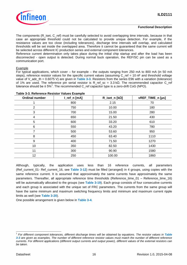
The components (R_iset, C_ref) must be carefully selected to avoid overlapping time intervals, because in that case an appropriate threshold could not be calculated to provide unique detection. For example, if the resistance values are too close (including tolerances), discharge time intervals will overlap, and calculated thresholds will be set inside the overlapped area. Therefore it cannot be guaranteed that the same current will be selected across different IC production series and external component tolerances. Reference current determination only takes place during the initial chip startup and after the load has been disconnected - open output is detected. During normal buck operation, the REF/SC pin can be used as a communication port. Example For typical applications, which cover – for example – the outputs ranging from 250 mA to 800 mA (in 50 mA steps), reference resistor values for the specific current values (assuming C_ref = 10 nF and threshold voltage value of V_adc_th = 0.6075 V) are given in Table 3-3. Resistors from the series E96 with a variation (tolerance) of 1% are used. The reference pin serial resistor is R_ref_sc = 3.3 kΩ. The recommended capacitor C_ref tolerance should be ≤ 5%
1. The recommended C_ref capacitor type is a zero-drift CoG (NPO).
Table 3-3. Reference Resistor Values Example
Ordinal number I_ref_n [mA] R_iset_n [kΩ] vREF_TIME_n [µs]
1 800 2.15 70
2 750 10.00 180
3 700 15.00 280
4 650 21.50 430
5 600 33.20 610
6 550 43.20 780
7 500 53.60 950
8 450 63.40 1110
9 400 71.50 1270
10 350 82.50 1430
11 300 90.90 1580
12 250 100.00 1860
Although, typically, the application uses less than 16 reference currents, all parameters
(Ref_current_01- Ref_current_16, see Table 3-12) must be filled (arranged) in 4 groups, using copies with the
same reference current. It is assumed that approximately the same currents have approximately the same
parameters. Thereafter, all appropriate reference time thresholds (Reference_time_01 – Reference_time_16)
will be automatically allocated to the groups (see Table 3-19). Each group consists of four consecutive currents
and each group is associated with the unique set of FRC parameters. The currents from the same group will
have the same minimum and maximum switching frequency limits and minimum and maximum current ripple
limits as well (see Table 3-20).
One possible arrangement is given below in Table 3-4.
1 For different component tolerances, different discharge times will be obtained by equations. The resistor values in Table
3-3 are given as examples. The number of different reference resistor values must match the number of different reference currents. For different applications (different output currents and output power), different values of the external resistors can be taken.

ILD2111
Functional Description
Datasheet 17 Revision 1.0, 2015-04-08
Table 3-4. Reference Current Arrangement
Group number Reference Currents
1. 800 mA, 750 mA, 700 mA
2. 650 mA, 600 mA, 550 mA
3. 500 mA, 450 mA, 400 mA
4. 350 mA, 300 mA, 250 mA
3.3.4 Output Current Control and Measuring
The output current is measured at the CS pin by means of an external shunt resistor. The controller, using floating buck topology, operates in a Continuous Conduction Mode (CCM) and is realized as a hysteretic current controller. The average output current is regulated using minimum and maximum currents (IMAX and IMIN, see Figure 11). Maximum and minimum current values are defined with respect to allowed output current ripple. The maximum current is set as a true analog comparator threshold value using an internal DAC. The minimum current value is regulated by the internal PI regulator controlling TOFF time. When the MOSFET is turned on, TON is approximately given as follows (all resistances and voltage drops of used components are neglected):
𝑇𝑂𝑁 = (𝐼𝑀𝐴𝑋 − 𝐼𝑀𝐼𝑁) ∙𝐿𝐸𝑋𝑇
𝑉𝐼𝑁−𝑉𝑂𝑈𝑇= 𝐼𝑅𝐼𝑃𝑃𝐿𝐸 ∙
𝐿𝐸𝑋𝑇
𝑉𝐼𝑁−𝑉𝑂𝑈𝑇. (10)
When the MOSFET is turned off, TOFF is approximately given as follows (all resistances and voltage drops of used components are neglected):
𝑇𝑂𝐹𝐹 = (𝐼𝑀𝐴𝑋 − 𝐼𝑀𝐼𝑁) ∙𝐿𝐸𝑋𝑇
𝑉𝑂𝑈𝑇= 𝐼𝑅𝐼𝑃𝑃𝐿𝐸 ∙
𝐿𝐸𝑋𝑇
𝑉𝑂𝑈𝑇. (11)
where VIN and VOUT are the input and output voltages respectively and LEXT is the buck inductance.
Therefore, the switching frequency of the buck cycle can be rendered as:
𝑓𝑆𝑊 =1
𝑇𝑂𝑁+𝑇𝑂𝐹𝐹=
1
𝐼𝑅𝐼𝑃𝑃𝐿𝐸∙𝐿𝐸𝑋𝑇∙(1
𝑉𝐼𝑁−𝑉𝑂𝑈𝑇+
1
𝑉𝑂𝑈𝑇). (12)

ILD2111
Functional Description
Datasheet 18 Revision 1.0, 2015-04-08
tt = 0
IMAX
IMIN
Inductor current
MOSFET switching
Shunt current(current sense)
TON TOFF...
TON
TOFF
IMAX
IMIN
IMEAN IRIPPLE
TSW
Figure 11. Sampled Current
When the current reaches its maximum value (IMAX), the MOSFET is turned off for a duration of TOFF, which is defined by the output of the PI regulator. After this interval elapses, the MOSFET is turned on again, the minimum current (IMIN) is sampled and the mean current for the entire PWM interval is calculated as:
𝐼𝑀𝐸𝐴𝑁 =𝐼𝑀𝐴𝑋+𝐼𝑀𝐼𝑁
2. (13)
The minimum current samples are averaged and averaging happens every 16 switching cycles. This average value is then compared to a reference providing an error signal for the PI regulator, as shown in Figure 12. Based on that error, the PI regulator calculates the new TOFF time resulting in output current regulation, hence closing the regulation loop.
R_current_sense
ton toff
IMIN Current Measurement
Minimal Current
IMIN reference
+
-
PIController
DrivingLogic
IMINREF
IMIN
TOFF
Error signal
IMIN
IMAX
Figure 12. Hysteretic Current Regulator

ILD2111
Functional Description
Datasheet 19 Revision 1.0, 2015-04-08
PI regulator parameters can be adjusted for faster transient response (dynamic behavior) during startup and more stable output current during normal steady-state operation. These constants (PI_shift_softstart_lc, PI_gain_shift_softstart_hc, PI_gain_shift_lc and PI_gain_shift_hc, see Table 3-17) are divided into two groups depending on the current range (constant Ref_current_HCTH, see Table 3-14) and operating conditions (startup or normal). Constants for low currents (low range - LC) typically have larger values than high current parameter values (high range - HC) because, for lower currents, the error signal has to be multiplied by a larger number (Gain) to obtain appropriate behavior regarding response and stability of the output current.
3.3.5 Current Startup, Soft-Start and Shutdown Control
Current soft-start and shutdown control is implemented in order to keep the input voltage VIN and supply voltage VCC, which come from the primary stage (usually a flyback converter with a transformer auxiliary winding for VCC voltage), within the operating range and stable. During the soft-start time, the output (mean) current increases slowly with programmable parameters. The startup current is defined by the constant Softstart_start_curr (see Table 3-16). Current and time steps are defined by the constant Softstart_curr_step (see Table 3-16) and parameter Softstart_time_step respectively (see Table 3-11, green line in Figure 13). The time step can be set as a number of system ticks (the default value is 100 μs). If any of the step (ICSUS = Softstart_curr_step or tCSUS = Softstart_time_step) values is zero, the buck converter will start with a 100% current, and without soft-start. During soft shutdown time, the output current decreases slowly with programmable current and time steps (constant Softshutdown_curr_step - Table 3-16 and parameter Softshutdown_time_step - Table 3-11, see red line in Figure 13). Hence, the input voltage VIN and supply voltage VCC remain in the operating range and the device will work correctly. If the soft shutdown is not enough to provide an appropriate operating range (for VIN and VCC), some minimum current (ERROR CURRENT – IERROR) defined by the parameters Err_refcurrent_max and Err_refcurrent_min (see Table 3-9 and Figure 13) will be generated for a defined time period (error time). When this time interval has elapsed (Error time timeout – constant Err_current_time, see Table 3-14), the output current is zero. If the current soft shutdown is not needed, it is necessary to set either the parameter to zero (ICSDS = Softshutdown_curr_step or tCSDS = Softshutdown_time_step).
t
IOUT (MEAN CURRENT)
Soft START time Normal operation Soft SHUT-DOWN time
ICSUS
ICSDS
tCSDS
tCSUS
ICSUS – ConsttCSUS – Softstart_time_step
ICSDS – ConsttCSDS – Softshutdown_time_step
ERROR CURRENT
Error time
IERROR
IREF_CURRENT
Ierr_cur_max = Err_refcurrent_maxIerr_cur_min = Err_refcurrent_min
IERROR = (Ierr_cur_max + Ierr_curr_min) / 2
Figure 13. Soft-Start and Soft Shutdown Definitions

ILD2111
Functional Description
Datasheet 20 Revision 1.0, 2015-04-08
3.4 Current Ripple vs. Switching Frequency Control Scheme
The switching frequency and output current ripple must be handled in such a way as to ensure that the efficiency is as high as possible and that the ripple is in a proper range with sufficient margin to the specified maximum. Two options for implementing a suitable system are described below.
3.4.1 Fixed Current Ripple
For a fixed current ripple, it is necessary to choose an appropriate value for the current ripple (parameter Curr_ripple_perc, see Table 3-12) so the switching frequency does not exceed the maximum allowed frequency around the output voltage VOUT = VIN/2. The maximum switching frequency should not exceed 250 kHz. Examples for three different current values are shown in Figure 14.
Figure 14. Switching Frequency vs. Output Voltage for Constant Output Current Ripple Iripple = 30%
10
15
20
25
30
35
0
50
100
150
200
250
300
0 10 20 30 40 50 60
Irip
ple
[%
]
fsw
[kH
z]
Vout [V]
fsw(Vout), Iripple=const
fsw(800mA) fsw(550mA) fsw(350mA) Iripple

ILD2111
Functional Description
Datasheet 21 Revision 1.0, 2015-04-08
3.4.2 Frequency and Ripple Control
The ILD2111 supports a powerful Frequency Ripple Controller (FRC) because the switching frequency of the Buck converter is not constant due to different loads (different number of LEDs leading to different output voltages). The main idea is to stabilize the operating point within configurable limits (operating area – green field, see Figure 15). During startup and normal operation, the frequency-ripple control update interval is defined by the constants FRC_reg_interval_start and FRC_reg_interval_oper (see Table 3-20). The number of FRC passes, before being considered steady, is defined by the constant FRC_pass_oper_th (see Table 3-20).
Operating Area
fsw
IrippleIripple_maxIripple_min
fsw_max
Adjustable
Starting Point
A
B
C
D
A, B, C, D
Corrected Operating Points
fsw_min
Starting Point
Starting Point
Starting Point
Figure 15. FRC Operating Area All reference current values will be arranged in four groups (see Table 3-12) where currents from the same group have the same switching frequency and current ripple limits, as explained in Section 3.3.3. For each group, there are predefined (available) parameters and constants (see Table 3-12 and Table 3-20):
1) Curr_ripple_perc – Initial (starting) current ripple (in percentage form). 2) Curr_ripple_min_(group) – Minimum allowed ripple value (minimum absolute output current ripple
value, Iripple_min in mA, not in percentage form). 3) Curr_ripple_max_(group) – Maximum allowed ripple value (maximum absolute output current ripple
value, Iripple_max in mA, not in percentage form). 4) FRC_freq_min_limit_(group) – Maximum allowed TPWM (defining the minimum switching frequency
allowed, fsw_min). 5) FRC_freq_max_limit_(group) – Minimum allowed TPWM (defining the maximum switching frequency
allowed, fsw_max).

ILD2111
Functional Description
Datasheet 22 Revision 1.0, 2015-04-08
An example is provided below for better understanding. The following parameters apply in this example for IOUT = 350 mA:
1. Iripple_init = 30% (or 105 mA) – Initial starting current ripple.
2. Iripple_min = 25% (or 87.5 mA) – Minimum allowed current ripple.
3. Iripple_max = 50% (or 175 mA) – Maximum allowed current ripple.
4. fsw_min = 100 kHz (or TPWM_max = 1/fsw_min = 10 µs) – Minimum allowed switching frequency.
5. fsw_max = 150 kHz (or TPWM_min = 1/fsw_max = 6.67 µs) – Maximum allowed switching frequency.
The Frequency Ripple Control algorithm works as following:
The system begins to operate with the defined ripple, which is given as a percentage of the average current (e.g. Iripple_init = 30% IOUT). This value is used to calculate the maximum (adding the half-ripple value to the reference current value) and minimum (subtracting the half-ripple value to the reference current value) hysteretic currents. There are several possible cases depending on the output voltage:
1) If the achieved operating frequency is within allowed borders (defined by fsw_min and fsw_max), and the starting value of the ripple is within allowed absolute ripple borders (defined by Iripple_min and Iripple_max), no correction will be performed (e.g. Vout = 10 V – orange curve, operating point B is in the operating area, B=B’, see Figure 16).
2) If the achieved operating frequency is above the maximum allowed switching frequency fsw_max (e.g. Vout = 15 V – grey curve, point C; Vout = 20 V – yellow curve, point D), the firmware will start to slowly increase the ripple in order to lower the operating frequency (the slope of this increasing ripple depends on the buck inductance LEXT, see equation (12) on page 17). It will continue increasing the ripple until the frequency falls below the high threshold fsw_max (corrected points C’ and D’, see Figure 16).
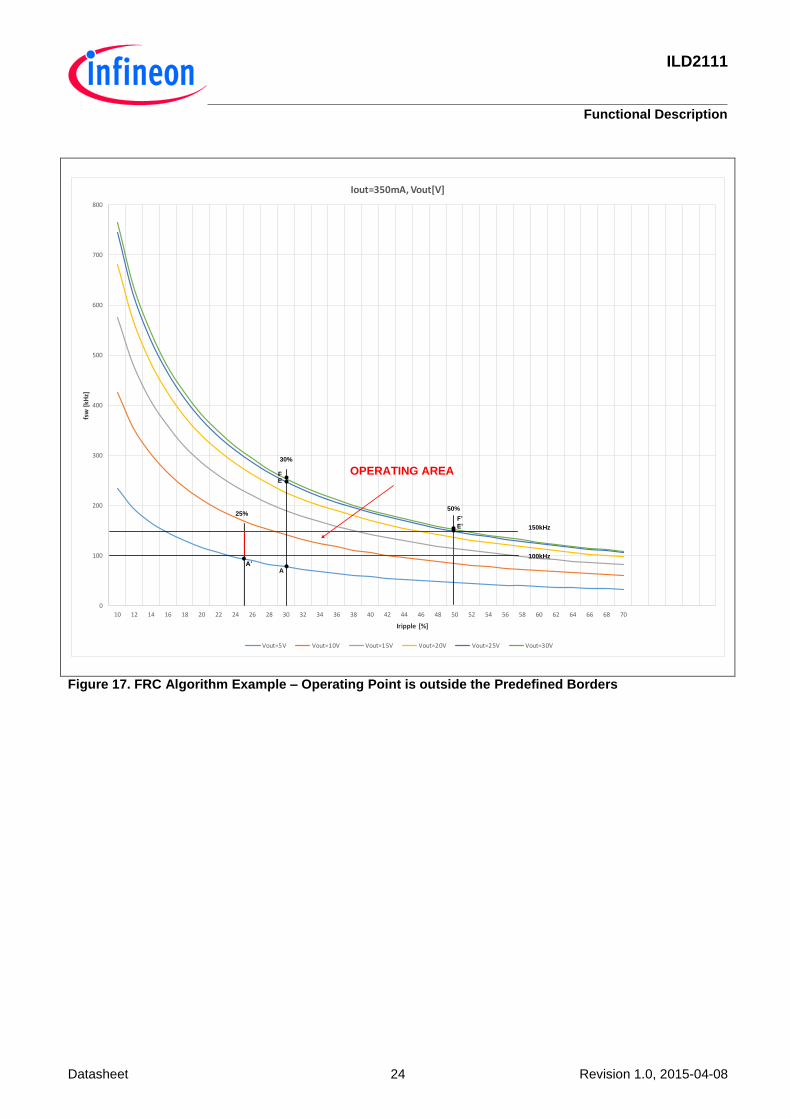
3) If the achieved operating frequency is above the maximum allowed switching frequency fsw_max (e.g. Vout = 25 V – dark blue curve, point E; Vout = 30 V – green curve, point F), the firmware will start to slowly increase the ripple in order to lower the operating frequency (the slope of this increasing ripple depends on the buck inductance LEXT, see equation (12) on page 17). It will continue increasing the ripple until it hits its maximum allowed value Iripple_max. The switching frequency will be determined by Iripple_max and could be outside the predefined borders (corrected points E’ and F’, see Figure 17).
4) If the achieved operating frequency is below the minimum allowed switching frequency fsw_min (e.g. Vout = 5 V – blue curve, point A), the firmware will start to slowly decrease the ripple in order to raise the operating frequency (the slope of this decreasing ripple depends on the buck inductance LEXT, see equation (12) on page 17). It will continue decreasing the ripple until the frequency reaches the low threshold value defined by the parameter fsw_min, or if the ripple hits the minimum allowed value defined by the parameter Iripple_min. In this case, the switching frequency could be outside the predefined borders (corrected point A’, see Figure 17).

ILD2111
Functional Description
Datasheet 23 Revision 1.0, 2015-04-08
Figure 16. FRC Algorithm Example – Operating Point successfully put into Operating Area
0
100
200
300
400
500
600
700
800
10 12 14 16 18 20 22 24 26 28 30 32 34 36 38 40 42 44 46 48 50 52 54 56 58 60 62 64 66 68 70
fsw
[kH
z]
Iripple [%]
Iout=350mA, Vout[V]
Vout=5V Vout=10V Vout=15V Vout=20V Vout=25V Vout=30V
100kHz
150kHz
OPERATING AREA
25%50%
30%
B
C
D
B’ C’ D’
ILD2111
Functional Description
Datasheet 24 Revision 1.0, 2015-04-08
Figure 17. FRC Algorithm Example – Operating Point is outside the Predefined Borders
0
100
200
300
400
500
600
700
800
10 12 14 16 18 20 22 24 26 28 30 32 34 36 38 40 42 44 46 48 50 52 54 56 58 60 62 64 66 68 70
fsw
[kH
z]
Iripple [%]
Iout=350mA, Vout[V]
Vout=5V Vout=10V Vout=15V Vout=20V Vout=25V Vout=30V
100kHz
150kHz
OPERATING AREA
25%50%
30%
A
EF
A’
E’
F’

ILD2111
Functional Description
Datasheet 25 Revision 1.0, 2015-04-08
An example of a frequency ripple control scheme is shown below in Figure 18, Figure 19 and Figure 20. Resistances and voltage drops of used components (VD – forward voltage of the freewheeling diode, RL – inductor resistance, RON = RDS – channel resistance when the MOSFET is ON, RCS – shunt resistance connected to the CS pin, VOUT = N·VLED+N·RLED·IOUT – output voltage (LED lighting load), N – number of LEDs,
VLED – LED forward voltage, RLED – LED forward resistance) are included in calculations.
Figure 18. 800 mA FRC Scheme
Figure 19. 550 mA FRC Scheme
0
5
10
15
20
25
30
35
0
20
40
60
80
100
120
0 10 20 30 40 50 60
Irip
ple
[%
]
fsw
[kH
z]
Vout [V]
FRC scheme for Iout=800 mA
fsw Iripple
10
15
20
25
30
35
40
45
0
20
40
60
80
100
120
140
0 10 20 30 40 50 60
Irip
ple
[%
]
fsw
[kH
z]
Vout [V]
FRC scheme for Iout=550 mA
fsw Iripple

ILD2111
Functional Description
Datasheet 26 Revision 1.0, 2015-04-08
Figure 20. 350 mA FRC Scheme Frequency Ripple Controller behavior depends on the output voltage load as mentioned before. As can be seen in previous figures, the FRC regulates the switching frequency and current ripple for this dedicated example as follows:
1st area – Vout <10 V: The system will be started with the minimum constant switching frequency and
the ripple will increase accordingly.
2nd
area – 10 V < Vout < 15 V approximately: The system will be started with a selectable initial current
ripple (30% of Iout). The switching frequency will be changed accordingly (not valid for 800 mA).
3rd
area – 15 < Vout < 25 V approximately: The system will be started with the maximum frequency
value; it will be kept constant at a predefined value and the current ripple will increase accordingly (not
valid for 800 mA).
4th area – Vout ≈ VIN/2: The system is started with the maximum predefined current ripple, but the
frequency cannot be kept within predefined borders, which means that the frequency will be determined
by the TOFF and Iripple values and external hardware components.
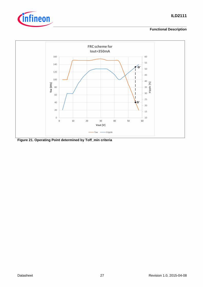
5th area – Vout > 45 V (near VIN) approximately: TOFF_min criteria have the highest priority
1, so the
frequency and ripple will have the values determined by the external hardware components (not by
FRC) and can be outside the defined limits.
1 If the high voltage load is applied at the output (large number of LEDs, the output voltage is near the input voltage), the
operating frequency will be low and if it falls below fsw_min, the frequency-ripple controller will start to correct it by decreasing
the ripple value, as described above. On the other hand, due to the high output voltage, TOFF is quite short (see equation
(11) on page 17). It is very important that the turn-off time must be longer than the predefined TOFF_min time (constant
Toff_min, see Table 3-19), because during that time all calculations must be performed before starting a new cycle. At that
point, the frequency-ripple controller starts to increase the ripple again in order to meet TOFF_min criteria. The final outcome is
that the current ripple and switching frequency could stay outside the predefined limits (above I ripple_max and below fsw_min
respectively) – point G’ in Figure 21. If TOFF falls below the minimum allowed value (low ripple means short TOFF time for
constant output voltage), the regulator cannot maintain the average current any longer, therefore influencing accuracy. If
parameters are configured properly, any of above mentioned actions lead to stable operating conditions for the given
current/load situation. However, there is drift in the operating frequency produced by the input voltage ripple that has to be
taken into account when deciding on parameter values. The frequency ripple controller will always try to put the operating
point into the operating area, but its final position will depend on the other criteria that affect its position.
10
15
20
25
30
35
40
45
50
55
60
0
20
40
60
80
100
120
140
160
0 10 20 30 40 50 60
Irip
ple
[%
]
fsw
[kH
z]
Vout [V]
FRC scheme for Iout=350 mA
fsw Iripple
ILD2111
Functional Description
Datasheet 27 Revision 1.0, 2015-04-08
Figure 21. Operating Point determined by Toff_min criteria
10
15
20
25
30
35
40
45
50
55
60
0
20
40
60
80
100
120
140
160
0 10 20 30 40 50 60
Irip
ple
[%
]
fsw
[kH
z]
Vout [V]
FRC scheme for Iout=350mA
fsw Iripple
G’
G’

ILD2111
Functional Description
Datasheet 28 Revision 1.0, 2015-04-08
3.5 Input Voltage Measurement and Calibration
There are some indirect measurements, like the output voltage VOUT and output power POUT, that take input voltage measurement as an input. Therefore the accuracy of those measurements depends on the input voltage VIN accuracy, and typically is lower due to the accuracies of other variables. Therefore it is important that the input voltage is accurately measured. The input voltage is sensed at the VIN pin. A filter capacitor CVIN (typically 100 nF) is used for voltage (at the pin VIN) filtering of conductive and electromagnetic interference caused by the converter switching operation. The measurement circuit is shown in Figure 22 below.
VIN
R_vin
VIN
ADC
GND
IMEAS
S
H
U
N
T
ILD2111
CVIN
Figure 22. Input Voltage Measurement Schematic
Two measurement ranges related to the VIN pin are implemented. They are called current ranges because calibration is based on the current flowing into the VIN pin. The two ranges use a different value of the internal shunt resistor, where ADC measures the voltage drop. The reason for calibration is to make results independent of RSHUNT production tolerance by including the measured value of RSHUNT as part of internal chip calibration data during chip production.
Nominal shunt values for an appropriate current range are as follows:
1) Current range 00b => IMEAS = 209 µA, RSHUNT = 6690 Ω.
2) Current range 01b => IMEAS = 1.6 mA, RSHUNT = 1490 Ω. The current range is defined by the parameter Vin_current_range (see Table 3-8). Depending on the input voltage range to be measured, for lower power dissipation, the value of the external resistor R_vin and the maximum current measurement range must be chosen carefully. Especially for high VIN voltage (bus voltage), power dissipation needs to be considered as part of system losses. For more details, see the examples below.

ILD2111
Functional Description
Datasheet 29 Revision 1.0, 2015-04-08
Examples:
1) If the maximum bus voltage is high, e.g. VINMAX = 500 V, the current measurement range (209 µA) should be chosen to minimize power dissipation over R_vin. The value of the external resistor R_vin is obtained from the equation below (209 µA would ideally be full scale at the ADC; to achieve accurate measurement over the production spread of ILD2111, use a margin factor of 75%).
Therefore,
𝑅_𝑣𝑖𝑛 =𝑉𝐼𝑁𝑀𝐴𝑋
0.75∙𝐼209µ𝐴− 𝑅𝑆𝐻𝑈𝑁𝑇 = 3.18 MΩ. (14)
2) If the maximum bus voltage is lower, e.g. VINMAX = 80 V, the current measurement range (1.6 mA) should be chosen. Therefore,
𝑅_𝑣𝑖𝑛 =𝑉𝐼𝑁𝑀𝐴𝑋
0.75∙𝐼1.6𝑚𝐴− 𝑅𝑆𝐻𝑈𝑁𝑇 = 65.2 kΩ. (15)

ILD2111
Functional Description
Datasheet 30 Revision 1.0, 2015-04-08
3.6 Protection Features
Table 3-5 gives an overview of the supported protection features. Two protection modes are implemented (auto restart mode and latch mode), which can be entered. Protection features can be configured by the parameters that are shown in Table 3-9 and Table 3-10. An error counter counts errors up to 4 restarts, defined by the constant value Err_restart_tries (see Table 3-14). The error counter is reset when the device operates without additional errors for the time defined by the constant Err_cnt_clear_time (see Table 3-14), or at the startup sequence, e.g. if VCC falls below the voltage threshold (see Table 4-4).
Table 3-5. Protection Features
Undervoltage Protection for DC Input Line – VIN Undervoltage Section 3.6.1
Overvoltage Protection for DC Input Line – VIN Overvoltage Section 3.6.2
Output Undervoltage Protection – VOUT Undervoltage Section 3.6.3
Open Output Protection Section 3.6.4
Output Overvoltage Protection – VOUT Overvoltage Section 3.6.5
Output Overpower Protection – POUT Overpower Section 3.6.6
Overtemperature Protection Section 3.6.7
Overcurrent Protection – Level 2 (OCP2) Section 3.6.8
Functional Protections Section 3.6.9

ILD2111
Functional Description
Datasheet 31 Revision 1.0, 2015-04-08
Protection functions are shown in a matrix in Table 3-6 below. Table 3-6. Protection Functions Matrix
Description of Fault Characteristics of Fault
Operating Mode Detection Active
Consequence
Nam
e o
f F
ault
Min
imum
Dura
tion
of eff
ect
Sta
rtu
p
Norm
al
Shutd
ow
n
Err
or
Curr
ent
Buck O
FF
VIN Undervoltage INPUV 1.6 ms X X - - - Startup - Waits until condition is removed Normal – Auto-restart
VIN Overvoltage INPOV 1.6 ms X X - - - Startup - Waits until condition is removed Normal – Auto-restart
VOUT Undervoltage OUTUV 0.8 ms @40 kHz
- X - - - Auto-restart mode with 4 tries (restarts). After 4 failed attempts, the device enters latch mode
Open Output OPEN 1)
X X - - - Auto-restart mode with 4 tries (restarts). In each restart try, I-set procedure will be executed. After 4 failed attempts, the device enters latch mode
VOUT Overvoltage OUTOV 0.4 ms @40 kHz
- X - - - Auto-restart mode with 4 tries (restarts). After 4 failed attempts, the device enters latch mode
POUT Overpower PWR 6.4 ms @40 kHz
- X - - - Auto-restart mode with 4 tries (restarts). After 4 failed attempts, the device enters latch mode
Overtemperature (Internal or External)
OTI or OTE
0.4 ms @40 kHz
X X - - - Startup - Waits until condition is removed Normal – Auto-restart
OCP2 OCP Instantly X X - - - The device is in predefined time loop until the device is switched off or when the cause of the OCP2 event is removed – see Section 3.6.8
X = Checked during Operating Mode - = Not checked during Operation Mode
In each restart attempt, the IC remains in a time loop whose duration is determined by the constant Err_restart_time, see Table 3-14
1) Defined by constant Open_out_timeout, see Section 3.6.4 .
All protections are described in the following sections.
ILD2111
Functional Description
Datasheet 32 Revision 1.0, 2015-04-08
3.6.1 Undervoltage Protection for DC Input Line – VIN Undervoltage
Undervoltage protection for the DC input line prevents the device from operating with an excessively low VIN voltage. If the input voltage is below the specified value, the output current is turned off. The device waits until the input undervoltage (low voltage value) condition is removed (Vin_min_start is met) and then starts with output current generation again. There are two hysteretic input voltage values that are used as thresholds during the startup sequence (upper threshold value – parameter Vin_min_start, see Table 3-9)
1 and during
operation (lower threshold value – parameter Vin_min_oper, see Table 3-9)1. If the input voltage is VIN
< Vin_min_oper during operation, the buck converter will be shut down and will wait for the VIN startup condition (when Vin_min_start is reached). This event does not affect the error counter.
3.6.2 Overvoltage Protection for DC Input Line – VIN Overvoltage
Overvoltage protection for the DC input line prevents the device from operating with an excessively high VIN voltage. After the overvoltage condition on input is detected, the output current is turned off. The device waits for the input overvoltage condition to be removed (Vin_max_start is met) and then starts output current generation again. There are two hysteretic input voltage values that are used as thresholds during the startup sequence (lower threshold value – parameter Vin_max_start, see Table 3-9)
1 and during operation (upper threshold value
– parameter Vin_max_oper, see Table 3-9)1. If the input voltage is VIN > Vin_max_oper during operation, the
buck converter will be shut down and will wait for the VIN startup condition (when Vin_max_start is reached). This event does not affect the error counter.
3.6.3 Output Undervoltage Protection – VOUT Undervoltage
Output undervoltage protection prevents the device from operating with an excessively low output voltage VLEDmin or when LED output is lowered. If the output voltage is lower than the minimum value VOUT < Vout_min, an undervoltage output is detected, and the device enters error auto-restart mode with 4 tries (restarts) – constant Err_restart_tries (see Table 3-14). After 4 failed attempts, the device enters latch mode. The minimum output operating voltage value is programmable (parameter Vout_min, Table 3-9). Undervoltage output is checked during steady-state condition, after completing soft-start. The restart timeout startup delay is predefined by the constant Err_restart_time (see Table 3-14).
3.6.4 Open Output Protection
Open output protection prevents the device from operating when no load on output is detected. It is detected when the time to achieve IMAX (see Figure 11) exceeds the value of the parameter Open_out_timeout (see Table 3-14)
2. If the open output condition is detected, the device enters error auto-restart mode with 4 tries
(restarts) – constant Err_restart_tries (see Table 3-14). In each attempt, the device executes the reference resistor reading procedure (I-set procedure, see Section 3.3.3). The duration of the I-set procedure is defined by the parameter RC_measurement_timeout (duration = 2 · RC_measurement_timeout, see Table 3-19). The restart timeout startup delay is predefined by the constant Err_restart_time (see Table 3-14). After 4 failed attempts, the device enters latch mode. The total duration of the restart attempt can be obtained as the sum of the two above-mentioned times (I-set procedure + restart timeout). If the LED lighting load is connected (or replaced) at the output between two restart attempts, the I-set procedure will detect the new R_iset resistance and the buck converter will try to start with the newly determined reference current.
1 To minimize the impact of fluctuations on the exact VIN voltage value, filtering is implemented using a first-order filter whose
coefficient is defined by the constant Vin_filt_coef (see Table 3-14) 2 During buck ‘on time’ TON (see Figure 11), the gate driver stays constantly ‘high’ until IMAX is reached, or Open_out_timeout
expires. This can lead to a long ‘high’ time. In case there is a ‘high side driver’ circuit between the ILD2111 gate drive and MOSFET gate, proper functionality for all operating conditions needs to be considered. A stable OCP1 value (IMAX) is obtained by filtering defined by the constant Alt_OCP1_filt_stable (see Table 3-14)

ILD2111
Functional Description
Datasheet 33 Revision 1.0, 2015-04-08
3.6.5 Output Overvoltage Protection – VOUT Overvoltage
Output overvoltage protection prevents the device from operating when the high voltage at the output VOUT is detected
1. If the output voltage is higher than the maximum value VOUT > Vout_max, the device enters error
auto-restart mode with 4 tries (restarts) – constant Err_restart_tries (see Table 3-14). After 4 failed attempts, the device enters latch mode. The maximum output operating voltage value is programmable (parameter Vout_max, Table 3-9). Output voltage is checked during the steady-state condition, after completing soft-start. The restart timeout startup delay is predefined by the constant Err_restart_time (see Table 3-14).
3.6.6 Output Overpower Protection – POUT Overpower
Output overpower protection prevents damage to output components due to high output power2. The maximum
allowed output power value (parameter Pout_max, see Table 3-9) is set by the constants Pout_corr_LC and Pout_corr_HC (Pout_max_lc = Pout_corr_LC · Pout_max and Pout_max_hc = Pout_corr_HC · Pout_max) for low current and high current range respectively (see Table 3-14). The parameter Ref_current_HCTH decides between the low current and high current range (see Table 3-14). If the output power exceeds the maximum allowed operational value, the device enters error auto-restart mode with 4 tries (restarts) – constant Err_restart_tries (see Table 3-14). After 4 failed attempts, the device enters latch mode. Output overpower is checked during the steady-state condition after completing soft-start. The restart timeout startup delay is predefined by the constant Err_restart_time (see Table 3-14).
1 Output voltage is internally calculated, based on VIN and TON / TPWM duty factor. Output voltage can be calculated
approximately as VOUT = D * VIN = (TON / TPWM) * VIN (all resistances and voltage drops of used components are neglected). To minimize the impact of fluctuations on the exact TPWM period value, filtering is implemented using a first-order filter whose coefficient is defined by the parameter Tpwm_filt_coef (see Table 3-14). 2 Output power is internally calculated, based on VIN, IOUT and TON / TPWM ratio. The actual TON / TPWM ratio (for true output
power) also depends on parasitic effects (e.g. MOSFET diode reverses recovery time, additional circuit like high side driver). These parasitic effects are unknown to the chip calculation and need to be considered for choosing appropriate Pout_max values. To minimize the impact of fluctuations on the calculated POUT value, filtering is implemented using a first-order filter whose coefficient is defined by the parameter Pout_filt_coef (see Table 3-14) before comparing the output power against Pout_max_lc or Pout_max_hc thresholds.
ILD2111
Functional Description
Datasheet 34 Revision 1.0, 2015-04-08
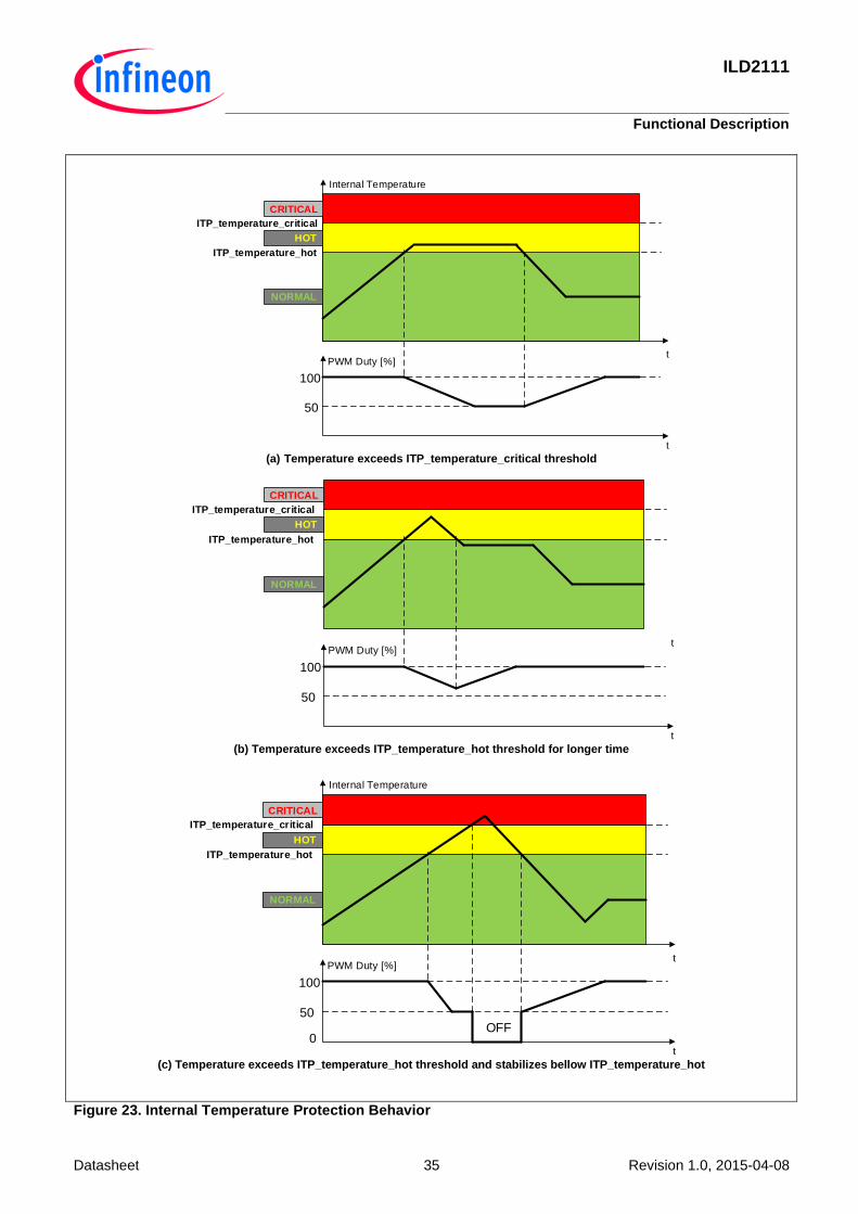
3.6.7 Overtemperature Protection
The ILD2111 supports overtemperature protection by means of internal and external temperature sensors. If both internal temperature protection and external temperature protection requests for the current level change, the lower current level will prevail. If the external sensor is not used (disabled by configuration), only the internal temperature protection is processed.
3.6.7.1 Internal Temperature Sensor – Internal PWM Dimming 1
Internal temperature-based protection uses internal temperature sensor measurement for reduction of the output current in the case that device temperature increases. For this purpose, two temperature thresholds - T1 and T2 - are defined (parameters ITP_temperature_hot – T1 and ITP_temperature_critical – T2 increasing in value – see Table 3-10) as well as one up-slope (constant ITP_PWM_inc_step - Table 3-15 and parameter ITP_PWM_inc_time_step - Table 3-10) and one down-slope (constant ITP_PWM_dec_step - Table 3-15 and parameter ITP_PWM_dec_time_step - Table 3-10). Temperature thresholds can be set in steps of 1°C and slopes as percentages of the average current per minute. The output current level is reduced by PWM modulation with a programmable frequency rate – see Figure 28.
There are three temperature-related operating conditions:
- Normal T<=T1 - Hot T1<T<=T2 - Critical T>T2
Temperature measurement may lead to a change of operating state:
In the critical state, the output current is off. An output current restart could be in hot or normal state (default). If the device starts in hot mode, then the current is adjusted with the dedicated constant value (ITP_startup_PWM_hot = 50%, see Table 3-15). If it is in normal mode, it will start with 100% of the rated current.
In the hot state, the current will be reduced (decreased) according to a constant-defined limit (TP_PWM_duty_min = 50%, see Table 3-18) and down-slope. If the device starts in hot mode, it will start with 100% of the rated current, but then the current is adjusted with the dedicated parameter (ITP_startup_PWM_hot = 50%). In normal mode, the full current level (100%) is started and kept stable (no change in current level).
The complete device behavior regarding operating temperature conditions is shown in Figure 23, Figure 24 and Figure 28.
ILD2111
Functional Description
Datasheet 35 Revision 1.0, 2015-04-08
tPWM Duty [%]
100
t
NORMAL
HOT
CRITICAL
ITP_temperature_hot
ITP_temperature_critical
50
Internal Temperature
(a) Temperature exceeds ITP_temperature_critical threshold
tPWM Duty [%]
100
t
NORMAL
HOT
CRITICAL
ITP_temperature_hot
ITP_temperature_critical
50
(b) Temperature exceeds ITP_temperature_hot threshold for longer time
tPWM Duty [%]
100
t
NORMAL
HOT
CRITICAL
0OFF
ITP_temperature_hot
ITP_temperature_critical
50
Internal Temperature
(c) Temperature exceeds ITP_temperature_hot threshold and stabilizes bellow ITP_temperature_hot
Figure 23. Internal Temperature Protection Behavior

ILD2111
Functional Description
Datasheet 36 Revision 1.0, 2015-04-08
t
Internal Temperature
PWM Duty [%]
100
t
DITPDS
DITPDS – Internal Temperature protection PWM Duty factor decrement steptITPDS – Internal Temperature protection time decrement step
DITPIS
tITPIStITPDS
DITPIS – Internal Temperature protection PWM Duty factor increment steptITPIS – Internal Temperature protection time increment step
NORMAL
HOT
CRITICAL
DITPDS – Const
tITPDS – ITP_PWM_dec_time_step
DITPIS – Const
tITPIS – ITP_PWM_inc_time_step
ITP_temperature_hot
ITP_temperature_critical
50
Figure 24. Internal Temperature Protection

ILD2111
Functional Description
Datasheet 37 Revision 1.0, 2015-04-08
3.6.7.2 External Temperature Sensor – Internal PWM Dimming 2
External temperature-based protection uses a PTC resistor connected to the TS pin and GND (2-wire connection – Figure 25). External temperature is meant to reduce the output current in the case that the temperature of the light element increases (see LED lighting in Figure 25). For this purpose, two temperature thresholds, Te1 and Te2, are defined (parameters ETP_temperature_hot – Te1 and ETP_temperature_critical – Te2 increasing in value – see Table 3-10) as well as one up-slope (constant ETP_PWM_inc_step - Table 3-15 and parameter ETP_PWM_inc_time_step - Table 3-10) and one down-slope (constant ETP_PWM_dec_step - Table 3-15 and parameter ETP_PWM_dec_time_step - Table 3-10). Temperature thresholds can be set in steps of 1°C and slopes as percentages of the average current per minute. The output current level is reduced by PWM modulation with a programmable frequency rate – see Figure 28. To minimize the impact of fluctuations on the exact external temperature value, filtering is implemented using a first-order filter whose coefficient is defined by the constant ETP_filt_coef (see Table 3-15) before comparing against thresholds.
R_TS_pull_up
PTC
TS
C
ILD2111 LED
lighting
RPTC
VCC
ZD2V7GND
Figure 25. External Temperature Measurement
The external temperature sensor is supplied by VCC, whose actual value is read by the on-chip ADC and used to calculate the external temperature value (the reference value for VCC voltage compensation is defined by the parameter VCC_reference, see Table 3-10)
1. The TS pin is clamped via a 2.7 V Zener diode for protection
reasons.
The threshold levels vary according to the PTC resistance/temperature curve.
There are three temperature-related operating conditions:
- Normal T<=Te1 - Hot Te1<T<=Te2 - Critical T>Te2
Temperature measurement may lead to changes in the operating state2:
In the critical state, the output current is off. An output current restart could be in hot or normal state (default). If the device starts in hot mode, then the current is adjusted with the dedicated parameter (ETP_startup_PWM_hot = 50%, see Table 3-15). If it is in normal mode, it will start with 100% of the rated current.
1 To minimize the impact of fluctuations on the exact VCC voltage value, filtering is implemented using a first-order filter
whose coefficient is defined by the parameter Vin_filt_coef (see Table 3-14) 2 External temperature protection behavior curves have the same shape as internal temperature protection curves – see
Figure 23 (a, b and c).

ILD2111
Functional Description
Datasheet 38 Revision 1.0, 2015-04-08
In the hot state, the current will be reduced (decreased) according to a parameter-defined limit (TP_PWM_duty_min, see Table 3-18) and down-slope. If the device starts in hot mode, then the current is adjusted with the dedicated parameter (ETP_startup_PWM_hot = 50%). If it is in normal mode, it will start with 100% of the rated current.
In normal mode, the full current level (100%) will be kept (no change in current level). For startup in normal mode, 100% of the rated current will be generated at the output.
There is an additional ADC voltage threshold (constant ETP_temperature_disconnected, see Table 3-13) to improve existing functionality. It is not the temperature threshold. An ETP_temperature_disconnected internal threshold value signals that the ADC (voltage) value is too high – i.e., that the sensor is disconnected. If the sensor is disconnected during operation, PWM duty will be gradually reduced to a value defined by the constant TP_PWM_duty_min = 50% (see Table 3-18) as it is at a temperature defined by ETP_temperature_hot (see Figure 26). If the higher ADC voltage (greater than the ETP_temperature_disconnected value) is detected during startup, the sensor will be ignored during operation.
External temperature protection behavior is shown in Figure 26.
DETPDS – External Temperature protection PWM Duty factor decrement steptETPDS – External Temperature protection time decrement step
DETPIS – External Temperature protection PWM Duty factor increment steptETPIS – External Temperature protection time increment step
t
PWM Duty [%]
100
t
DETPDSDETPIS
tETPIStETPDS
NORMAL
HOT
CRITICAL
ETP_temperature_hot
ETP_temperature_critical
External Temperature
DETPDS – Const
tETPDS – ETP_PWM_dec_time_step
DETPIS – Const
tETPIS – ETP_PWM_inc_time_step
50
Figure 26. External Temperature Protection Behavior

ILD2111
Functional Description
Datasheet 39 Revision 1.0, 2015-04-08
3.6.8 Overcurrent Protection – Level 2 (OCP2)
To avoid damage to the shunt resistor or MOSFET due to the rapid increase (inrush) of the current through the shunt resistor (detected as the voltage at the CS pin), the overcurrent protection OCP2 is implemented as a hardware threshold. If the OCP2 threshold is reached
1 (regardless of the cause of its appearance), the gate
driver (power MOSFET) will be turned off automatically and can only be turned on again by firmware intervention. In the case of an OCP2 event, the firmware checks an internal counter of OCP2 events and applies a delay according to the table Table 3-7. After the delay the engine is reinitialized and the device starts operation. The OCP2 counter will be reset after a predefined time (constant Err_cnt_clear_time, see Table 3-14) in case there are no new OCP2 error events in the meantime. Otherwise, if the OCP2 event occurs again before the counter is reset, the number of errors is increased in increments up to the limit. Table 3-7. OCP2 Error Restart Delay
Number of the OCP2 events
Previous value of the OCP2 counter
Next value of the OCP2 counter
Restart delay
1 0 1 100 µs
2 1 2 500 µs
3 2 3 2500 µs
≥4 3 3 OCP2_restart_delay [ms]
The time loop defined by the constant OCP2_restart_delay (see Table 3-14) is repeated until the device is switched off or when the cause of the OCP2 event is removed. If the OCP2 condition is removed and the device is in internal or external PWM dimming, the device continues to operate in one of two modes (internal or external dimming), depending on which of the conditions for these modes is fulfilled.
3.6.9 Functional Protections
Beside previous protections related to an application, ILD2111 incorporated the functional protections in order to achieve high reliability of the operation.
3.6.9.1 Code Memory Protections
During the startup of the device, after a reset or power-up, firmware is copied from the OTP memory to the RAM. The firmware is then executed from the RAM. The firmware is signed with a CRC value (Cyclic Redundancy Check). During the process of copying, the CRC value is calculated and then compared to the signed CRC value. In the case of a mismatch the firmware will not start in order to prevent misbehavior.
During run time the RAM is protected by a parity check over one memory cell. RAM parity protection is a hardware feature which detects parity errors when RAM is accessed (read/write). In the event of a parity error, a hardware reset is issued and the device will restart accordingly.
3.6.9.2 Firmware Hang Protection
During run-time, the execution of the firmware can become erratic due to a hardware fault. In order to prevent such firmware “hangs” a watch dog timer (WDT) is utilized. The WDT is a hardware feature and if it is not serviced before a specific timeout, the device will reset and restart accordingly.
3.6.9.3 Parameter Memory Protection
The parameter memory is a dedicated part of the RAM. The device blank checks part of this area and also checks for the parameter “CRC error”. More details can be found in Section 3.9.2.
1 The digital representative of the OCP2 comparator output is digitally filtered. The number of successive samples that have
reached OCP2 level, after which OCP2 event will be acknowledged, is defined by the parameter OCP2_filt_stable (see Table 3-14).

ILD2111
Functional Description
Datasheet 40 Revision 1.0, 2015-04-08
3.7 External PWM Dimming
For external dimming, EPWM duty (DTEPWM - duty factor range 1% to 99%) and EPWM period (TEPWM) can be measured at the PWM input pin – see Figure 27.
PWMILD2111
t
TEPWM TEPWM
fEPWM = 100Hz - 1kHz
PWM-Dimming
PWM-Dimming
External
PWM Signal
GND
DTEPWM DTEPWM
fEPWM = 100Hz - 1kHz
Figure 27. External PWM Dimming The external PWM duty factor and external PWM frequency are obtained by measuring the on-time TON_EPWM (DTEPWM) and PWM period TEPWM. The timeout time for external PWM detection is defined by the constant EPWM_detection_timeout (see Table 3-18). There are two additional parameters that are used for external PWM processing: 1. LFPWM_threshold_divider, which represents the number of divisions by two of the measured TEPWM to obtain the hysteretic controller threshold and 2. LFPWM_flicker_free_threshold which represents the number of switching cycles that are considered flicker-free (the threshold divider is then not implemented for the hysteresis controller) – see Table 3-18. The complete output current PWM modulation is described in the following section 3.8.

ILD2111
Functional Description
Datasheet 41 Revision 1.0, 2015-04-08
3.8 Output Current PWM Modulation
Modulation of the output current can be requested by either of the following:
1. External PWM dimming signal (Section 3.7) and 2. Internal PWM dimming signal (internal temperature protection – see Section 3.6.7.1 and external
temperature protection – see Section 3.6.7.2).
The output current dimming PWM frequency, fPWM, will be defined by the external PWM dimming signal EPWM (the range of fEPWM is 100 Hz – 1 kHz; fEPWM = 1 / TPWM) or by the internal PWM signal (IPWM – constant value TP_PWM_period = 3.2 ms, fIPWM is 300 Hz, fIPWM = 1 / TPWM, see Table 3-18), if EPWM is not detected (the external EPWM frequency has a higher priority than the internal IPWM frequency). The final duty factor (PWM_Duty, see Figure 28) of the PWM signal will be determined by a minimum value of one of two calculated values (external epwm_duty or internal ipwm_duty).
iOUT
TPWM
PWM_ Duty
100%
tTPWM TPWM
PWM_ Duty
75%
PWM_ Duty
50%
IMEAN = IREF
iOUT
IMEAN = 75%IREF
IREF IREF
iOUT
IMEAN = 50%IREF
IREF
Figure 28. Output Current PWM Modulation A hysteretic controller is implemented in order to have a flicker-free output even at low dimming levels. This controller monitors the PWM duty and the high switching frequency period (buck cycle, T= TON + TOFF) and uses this information to control a number of switching cycles (N) within the PWM ON time. This number is updated only upon changes that are sufficiently high. The threshold is set to Told/2
LFPWM_threshold_divider. Therefore either the
PWM ON time changes to that extent or T changes such that |Tnew·N + TON_FIRST – TPWM_ON| > Told/2
LFPWM_threshold_divider. From the previous description it can be seen that the compensation for the first rising
slope time (TON_FIRST) is included in the calculation. The hysteretic cycle control requires reaching of the OCP1 level (IMAX) a minimum of three times, i.e. a minimum of two switching cycles 2·(TON + TOFF) plus a rising TON_FIRST and falling TOFF_LAST times in order to perform proper measurements and to regulate the current and implement protection features. Therefore, the minimum pulse width (TPWM_ON) of the output PWM dimming current is restricted according to this minimum duration (see Figure 29). The mean output current is proportional to the duty. However, for low duty, accuracy is lower due to limits mentioned earlier. Furthermore, the higher the output reference current value IREF, the greater the expected inaccuracy due to longer rising TON_FIRST and falling TOFF_LAST times.
iOUT
TPWM – PWM Cycle
TPWM_ON
t
IREF
IMEAN = (TPWM_ON/TPWM) * IREF
Buck cycleTON + TOFF
TON + TOFF
TPWM_ON
IMAX
IMIN
IRIPPLE
TON_FIRST TOFF_LAST
TPWM – PWM Cycle
TON_FIRST TOFF_LAST
TPWM – PWM Cycle
TON_FIRST TOFF_LAST
Figure 29. Output Current IMEAN Dimming Range Limitation
ILD2111
Functional Description
Datasheet 42 Revision 1.0, 2015-04-08
3.9 Configuration
This section provides an overview of the parameters that can be configured via the UART interface.
3.9.1 Overview of Configurable Parameters
The ILD2111 provides a generic firmware version that includes all parameters set to zero. The parameter values need to be specified by the user according to the target application. Please refer to the corresponding electrical characteristics in Section 4 for the minimum and maximum tolerances.
Parameter Lists
The parameter list contains the following groups:
- Configurable parameters (see Section 3.9.1.1) - Variable values that can be changed (modified) by the user according to the desired application.
- Design constants (see Section 3.9.1.2) - Constant values that cannot be changed and that are specified by the application.

ILD2111
Functional Description
Datasheet 43 Revision 1.0, 2015-04-08
3.9.1.1 Configurable Parameters
The configurable parameters are arranged in the following tables:
1. Hardware configuration - Table 3-8. 2. Protections - Table 3-9. 3. Temperature guard - Table 3-10. 4. Startup & shutdown - Table 3-11. 5. Output current set - Table 3-12.
Table 3-8. Configurable Parameters – Hardware Configuration
Parameter Name Minimum Value
Maximum Value
Description
Vin_current_range 0.209 mA 1.6 mA This bit field selects the measurement range for the current measurement (full scale value)
00B - Range 00 => IMEA = 209 µA (RSHUNT = 6690 Ω)
01B - Range 01 => IMEA = 1.6 mA (RSHUNT = 1490 Ω)
Current_sense_OCP1 0.4 V 0.6 V This bit field defines range (gain) for the CS OCP1 DAC, CS S&H and CS peak detector
10B - Range 10 = OCP1 = 0.6 V / OCP2 = 0.8 V (gain = 4)
11B - Range 11 = OCP1 = 0.4 V / OCP2 = 0.6 V (gain = 6)
GD_voltage 4.5 V 15 V Gate voltage settings
000B – 15 V
001B – 13.5 V
010B – 12 V
011B – 10.5 V
100B – 9 V
101B – 7.5 V
110B – 6 V
111B – 4.5 V
GD_current 30 mA 118 mA Gate current settings
00110B – 30 mA
00111B – 33 mA
01000B – 35 mA
01001B – 38 mA
01010B – 41 mA
01011B – 45 mA
01100B – 49 mA
01101B – 53 mA
01110B – 57 mA
01111B – 62 mA
10000B – 67 mA
10001B – 73 mA
10010B – 79 mA
10011B – 85 mA
10100B – 93 mA
10101B – 100 mA
10110B – 109 mA
10111B – 118 mA

ILD2111
Functional Description
Datasheet 44 Revision 1.0, 2015-04-08
Table 3-9. Configurable Parameters - Protections
Parameter Name Minimum Value
Maximum Value
Description
ETP_comp_Vcc Vcc voltage compensation for external temperature measurement enabled/disabled
ETP_enable External temperature protection feature enabled/disabled
Vin_min_start 0 Lowest possible input voltage VIN for buck converter
to be able to start operation.
Vin_min_oper 0 Lowest possible input voltage VIN allowed during
operation.
Vin_max_start 0 Highest possible input voltage VIN for buck converter
to be able to start operation
Vin_max_oper 0 Highest possible input voltage VIN allowed during
operation.
Vout_min 0 Minimum output voltage. Output voltage lower than
this value will trigger output undervoltage protection.
Vout_max 0 Maximum output voltage. Output voltage higher than
this value will trigger output overvoltage protection.
Pout_max
0 Maximum allowed output power – Output power higher than this value will trigger output overpower protection. The output power limit can be for Ref_currents < Ref_current_HCTH or for Ref_currents ≥ Ref_current_HCTH, see Table 3-14
Err_refcurrent_max Maximal hysteretic value of shutdown output current (ERROR CURRENT) - IERROR, see Figure 13
Err_refcurrent_min Minimal hysteretic value of shutdown output current (ERROR CURRENT) - IERROR, see Figure 13
Table 3-10. Configurable Parameters – Temperature guard
Parameter Name Minimum Value
Maximum Value
Description
ITP_temperature_hot1) -40 °C 150 °C Hot temperature threshold for internal sensor. ITP_temperature_critical1) -40 °C 150 °C Critical temperature threshold for internal sensor. ETP_temperature_hot 0 V 1.6 V Hot temperature voltage threshold for external
sensor. ETP_temperature_critical 0 V 1.6 V Critical temperature voltage threshold for external
sensor. ITP_PWM_inc_time_step 1 s 100 s Internal temperature protection time step (in
seconds) for current increasing (change of internal PWM duty).
ITP_PWM_dec_time_step
1 s 100 s Internal temperature protection time step (in seconds) for current decreasing (change of internal PWM duty).
ETP_PWM_inc_time_step
1 s 100 s External temperature protection time step (in seconds) for current increasing (change of internal PWM duty).

ILD2111
Functional Description
Datasheet 45 Revision 1.0, 2015-04-08
Parameter Name Minimum Value
Maximum Value
Description
ETP_PWM_dec_time_step 1 s 100 s External temperature protection time step (in seconds) for current decreasing (change of internal PWM duty).
Vcc_reference
11 V 24 V Reference value of Vcc voltage for external temperature measurement compensation.
1) Absolute maximum ratings and operation conditions need to be considered.
Table 3-11. Configurable Parameters – Startup & Shutdown1)
Parameter Name Minimum Value
Maximum Value
Description
Softstart_time_step 0 65535 Reference current ramp increment time interval (tCSUS) in system timer ticks (100 µs).
Softshutdown_time_step 0 65535 Reference current ramp decrement time interval (tCSDS) in system timer ticks (100 µs).
1) See Section 3.3.5.

ILD2111
Functional Description
Datasheet 46 Revision 1.0, 2015-04-08
Table 3-12. Configurable Parameters – Output Current Set1)
Parameter Name Minimum Value
Maximum Value
Description
Curr_ripple_perc 1 100 Current ripple percentage which is used during the startup sequence.
Ref_current_01 Reference current 01 which is assigned to the first FRC current group (FRC current group 1).
Ref_current_02 Reference current 02 which is assigned to the first FRC current group (FRC current group 1).
Ref_current_03 Reference current 03 which is assigned to the first FRC current group (FRC current group 1).
Ref_current_04 Reference current 04 which is assigned to the first FRC current group (FRC current group 1).
Ref_current_05 Reference current 05 which is assigned to the second FRC current group (FRC current group 2).
Ref_current_06 Reference current 06 which is assigned to the second FRC current group (FRC current group 2).
Ref_current_07 Reference current 07 which is assigned to the second FRC current group (FRC current group 2).
Ref_current_08 Reference current 08 which is assigned to the second FRC current group (FRC current group 2).
Ref_current_09 Reference current 09 which is assigned to the third FRC current group (FRC current group 3).
Ref_current_10 Reference current 10 which is assigned to the third FRC current group (FRC current group 3).
Ref_current_11 Reference current 11 which is assigned to the third FRC current group (FRC current group 3).
Ref_current_12 Reference current 12 which is assigned to the third FRC current group (FRC current group 3).
Ref_current_13 Reference current 13 which is assigned to the fourth FRC current group (FRC current group 4).
Ref_current_14 Reference current 14 which is assigned to the fourth FRC current group (FRC current group 4).
Ref_current_15 Reference current 15 which is assigned to the fourth FRC current group (FRC current group 4).
Ref_current_16 Reference current 16 which is assigned to the fourth FRC current group (FRC current group 4).
1) See Section 3.3.3.

ILD2111
Functional Description
Datasheet 47 Revision 1.0, 2015-04-08
3.9.1.2 Design Constants
Design constants are arranged in the following tables:
1. Hardware configuration - Table 3-13. 2. Protections - Table 3-14. 3. Temperature guard - Table 3-15. 4. Startup & shutdown - Table 3-16. 5. Control loop - Table 3-17. 6. Dimming - Table 3-18. 7. Output current set - Table 3-19. 8. Frequency ripple controller - Table 3-20.
Table 3-13. Design Constants – Hardware Configuration
Parameter Name Value Description
V_ADC_th 0.6075 V Ref capacitor discharge ADC voltage threshold.
ETP_temperature_disconnected 4000 i.u External sensor disconnection threshold value.
Table 3-14. Design Constants – Protections
Parameter Name Value Description
Ref_current_HCTH 800 mA First reference current value for HC range. The value should be selected from the reference current list.
Pout_corr_LC 1 POUT correction factor for low current (LC) range.
Pout_corr_HC 1 POUT correction factor for high current (HC) range.
Err_restart_tries 4 Number of auto-restart attempts before entering latch mode.
Err_current_time 500 ms Time interval (error time) after decreasing ramp to imply minimum current before turn off.
Err_restart_time 1000 ms Error auto-restart time interval.
Err_cnt_clear_time 65000 ms Time after which error restart attempts counter will be cleared.
Open_out_timeout 300 ms Open output detection time (timeout).
Alt_OCP1_filt_stable 2 ALTOCP1 filter length (OCP1 level).
OCP2_filt_stable 6 Number of samples that have reached OCP2 level, after which OCP2 event will be handled.
Pout_filt_coef 16 Output power first order filter coefficient. This parameter can be 2
n (n = 0, 1, 2, 3, 4, 5, 6, 7, 8). Pout filtering before
comparing against Pout_max_XX, (XX = LC, HC) threshold.
Vin_filt_coef 16 Vin voltage first order filter coefficient. This parameter can be 2
n (n = 0, 1, 2, 3, 4, 5, 6, 7, 8).
Tpwm_filt_coef 4 Tpwm (Buck cycle period) first order filter coefficient. This parameter can be 2
n (n = 0, 1, 2, 3, 4, 5, 6, 7, 8).
OCP2_restart_delay 130 ms Final delay time after four OCP2 events are detected.
Buck_steady_delay 32 Number of averaged PWM cycles for steady state operation where calculation & protection are handled.

ILD2111
Functional Description
Datasheet 48 Revision 1.0, 2015-04-08
Table 3-15. Design Constants – Temperature Guard
Parameter Name Value Description
ITP_PWM_inc_step 1 Internal temperature protection current increase step (internal PWM dimming).
ITP_PWM_dec_step 1 Internal temperature protection current decrease step (internal PWM dimming).
ITP_startup_PWM_hot 50% Internal temperature protection current de-rating PWM duty value for starting in the hot condition.
ETP_PWM_inc_step 1 External temperature protection current increase step (internal PWM dimming).
ETP_PWM_dec_step 1 External temperature protection current decrease step (internal PWM dimming).
ETP_startup_PWM_hot 50% External temperature protection current de-rating PWM duty value for starting in the hot condition.
ETP_filt_coef 64
External temperature measurement first order filter coefficient. External temperature filtering before comparing against thresholds. This parameter can be 2
n (n = 0, 1, 2, 3,
4, 5, 6, 7, 8).
Vcc_filt_coef 16 Vcc voltage first order filter coefficient. This parameter can be 2
n (n = 0, 1, 2, 3, 4, 5, 6, 7, 8).
Table 3-16. Design Constants – Startup and Shutdown
Parameter Name Value Description
Softstart_start_curr 5% Softstart starting value of reference current ramp (% of the
I_ref_01 current value). Ripple is given as a percentage.
Softstart_curr_step 0.5% Softstart reference current ramp increment step value (% of
the I_ref_01 current value).
Softshutdown_curr_step 0.5% Soft shutdown reference current ramp decrement step value
(% of the I_ref_01 current value).

ILD2111
Functional Description
Datasheet 49 Revision 1.0, 2015-04-08
Table 3-17. Design Constant – Control Loop
Parameter Name Value Description
PI_gain_shift_softstart_lc 3 PI regulator gain boost value for low current range during startup. The error signal is multiplied with 2
PI_gain_shift_softstart_lc
PI_gain_shift_softstart_hc 2 PI regulator gain boost value for high current range during startup. The error signal is multiplied with 2
PI_gain_shift_softstart_hc
PI_gain_shift_lc 1 PI regulator gain boost value for low current range during normal operation. The error signal is multiplied with 2
PI_gain_shift_lc.
PI_gain_shift_hc 0 PI regulator gain boost value for high current range during normal operation. The error signal is multiplied with 2
PI_gain_shift_hc.
Table 3-18. Design Constant – Dimming
Parameter Name Value Description
TP_PWM_period 3.2 ms Temperature protection internal IPWM period - defines the frequency of the internal IPWM dimming (fPWM = 1 / TP_PWM_period). fPWM ~ 300 Hz.
TP_PWM_duty_min 50% Temperature protection internal IPWM ON time - defines the duty factor (in %) of the internal IPWM dimming.
EPWM_detection_timeout 50 ms Timeout for external EPWM detection.
LFPWM_threshold_divider 1 Number of divisions by two of measured TPWM to get the hysteretic controller threshold. This parameter can be n = 0, 1, 2, 3, 4, 5, 6, 7, 8.
LFPWM_flicker_free_threshold 30 Number of switching cycles that are considered flicker-free (threshold divider is not implemented then for hysteresis controller).
ILD2111
Functional Description
Datasheet 50 Revision 1.0, 2015-04-08
Table 3-19. Design Constant – Output Current Set
Parameter Name Value Description
Reference_time_011)
* Discharge time threshold for Ref_current_01 Reference_time_02
1) * Discharge time threshold for Ref_current_02
Reference_time_031)
* Discharge time threshold for Ref_current_03
Reference_time_041)
* Discharge time threshold for Ref_current_04
Reference_time_051)
* Discharge time threshold for Ref_current_05
Reference_time_061)
* Discharge time threshold for Ref_current_06
Reference_time_071)
* Discharge time threshold for Ref_current_07
Reference_time_081)
* Discharge time threshold for Ref_current_08
Reference_time_091)
* Discharge time threshold for Ref_current_09
Reference_time_101)
* Discharge time threshold for Ref_current_10
Reference_time_111)
* Discharge time threshold for Ref_current_11
Reference_time_121)
* Discharge time threshold for Ref_current_12
Reference_time_131)
* Discharge time threshold for Ref_current_13
Reference_time_141)
* Discharge time threshold for Ref_current_14
Reference_time_151)
* Discharge time threshold for Ref_current_15
Reference_time_161)
* Discharge time threshold for Ref_current_16
RC_cap_charge_time 500 µs Time for charging ref capacitor.
RC_measurement_timeout 40000 µs Maximal time to determine that no external resistor has been connected during current set determination.
CS_blanking_time 0.758 µs Configurable leading edge blanking time.
CS_sample_time 0.622 µs Configurable CS sample time - delay until sampling starts.
Toff_min 0.4 µs Minimal TOFF time. It is 10% of TSWMIN = 1 / fSWMAX, fSWMAX = 250 kHz.
1) The calculated Reference_time values* (dependent on the selected reference resistors and reference
capacitor) will be assigned automatically to the appropriate reference current parameter Ref_current – see Section 3.3.3.

ILD2111
Functional Description
Datasheet 51 Revision 1.0, 2015-04-08
Table 3-20. Design Constant - Frequency Ripple Controller
Parameter Name Value Description
Curr_ripple_max_01_04 157 mA Maximum allowed ripple value for reference currents group 1. FRC is enabled.
Curr_ripple_min_01_04 87 mA Minimum allowed ripple value for reference currents group 1. FRC is enabled.
Curr_ripple_max_05_08 149 mA Maximum allowed ripple value for reference currents group 2. FRC is enabled.
Curr_ripple_min_05_08 87 mA Minimum allowed ripple value for reference currents group 2. FRC is enabled.
Curr_ripple_max_09_12 149 mA Maximum allowed ripple value for reference currents group 3. FRC is enabled.
Curr_ripple_min_09_12 87 mA Minimum allowed ripple value for reference currents group 3. FRC is enabled.
Curr_ripple_max_13_16 140 mA Maximum allowed ripple value for reference currents group 4. FRC is enabled.
Curr_ripple_min_13_16 87 mA Minimum allowed ripple value for reference currents group 4. FRC is enabled.
FRC_freq_max_limit_01_04 120 kHz Maximum allowed switching frequency (defines minimum allowed switching period) for reference currents group 1.
FRC_freq_min_limit_01_04 110 kHz Minimum allowed switching frequency (defines maximum allowed switching period) for reference currents group 1.
FRC_freq_max_limit_05_08 140 kHz Maximum allowed switching frequency (defines minimum allowed switching period) for reference currents group 2.
FRC_freq_min_limit_05_08 126 kHz Minimum allowed switching frequency (defines maximum allowed switching period) for reference currents group 2.
FRC_freq_max_limit_09_12 145 kHz Maximum allowed switching frequency (defines minimum allowed switching period) for reference currents group 3.
FRC_freq_min_limit_09_12 130 kHz Minimum allowed switching frequency (defines maximum allowed switching period) for reference currents group 3.
FRC_freq_max_limit_13_16 130 kHz Maximum allowed switching frequency (defines minimum allowed switching period) for reference currents group 4.
FRC_freq_min_limit_13_16 110 kHz Minimum allowed switching frequency (defines maximum allowed switching period) for reference currents group 4.
FRC_reg_interval_start 1024 Frequency-ripple control execution interval, during startup, in averaging intervals (averaging interval = 16 Buck cycles).
FRC_reg_interval_oper 12288 Frequency-ripple control execution interval during normal operation, in averaging intervals (averaging interval = 16 Buck cycles).
FRC_pass_oper_th 64 Number of FRC executions before considered steady and can switch to operational execution interval.

ILD2111
Functional Description
Datasheet 52 Revision 1.0, 2015-04-08
3.9.2 Configuration Procedure – Parameter Handling
The UART interface is configured at the pin REF/SC. The UART interface uses a single line for receiving and transmitting data. Firmware parameters are configured by means of communication protocol commands (Infineon proprietary protocol). Parameters are stored in on-chip OTP memory (default parameter block and parameter patches). Parameters can be accessed after the chip startup phase when VCC exceeds the VEXT threshold (see Table 4-4) and a UART connection at the REF/SC pin is detected. During startup, the application checks the default parameter block, RAM content that was copied from OTP memory. If no default parameter block is detected or if an error is found (CRC mismatch), buck operation will be disabled, and the device will report an error and enter the idle state. Reading and writing of the parameters are related to RAM parameter values. Write operations change the working value of the selected parameter, affecting chip operation after exiting configuration mode. The number of write operations is not limited. Since the default parameter block may be corrupted or in the case that the user wants to change some of the parameter values (or the whole parameter block), a patching feature can be used to change the parameters. In general, the patches will have the same structure as the default parameter block but the length will be arbitrary and up to the size of the full (default) block. A Cyclic Redundancy Check (CRC) in the patch will not reflect the patch data CRC, but rather the CRC of all the default parameters with the implemented patch. The patching procedure will be repeated for all found and consistent patches – see the parameter-handling flowchart in Figure 30.

ILD2111
Functional Description
Datasheet 53 Revision 1.0, 2015-04-08
STOP Buck operation.
Announces an error.
START
EXIT
NO
Is there
any patch?
Overwrite parameters in Default block with
appropriate parameters from the patch.
Replace CRC in the Default block.
Is there
additional patch?
Is Default
parameter block
consistent?
START Buck operation
YES
YES
NO
NO
YES
Does Default block
have correct CRC?
YES
NO
Figure 30. Parameter Handling In order to be presented to users in a suitable, comprehensive form, the .dp vision Graphical User Interface (GUI) application is provided by Infineon. This software tool relates parameter addresses and values to their appropriate physical interpretation. Moreover, default parameter settings can be changed (recalculated) according to application requirements (input voltage range, output current range, shunt resistor value, input voltage resistor value, reference capacitor value, etc.) and can be burned according to recalculated values as well as writing the corresponding patches. Burning parameters to OTP
1 will store the current parameter values
to be used as working values after the next chip reset. More information about .dp vision can be found in the User’s Manual document for this tool.
1 During burning, the OTP programming voltage VPP (see Table 4-15) must have a stable value.

ILD2111
Electrical Characteristics
Datasheet 54 Revision 1.0, 2015-04-08
4 Electrical Characteristics
4.1 Definitions
Figure 31 illustrates the definition for the voltage and current parameters used in this datasheet.
VPIN
PIN
GND
+IPIN
+ILD2111
Figure 31. Voltage and Current Definitions1
The electrical characteristics are arranged in the following tables:
1) Absolute Maximum Ratings, Table 4-1. 2) Thermal Characteristics, Table 4-2. 3) Operating Range, Table 4-3. 4) Electrical Characteristics of the Power Supply, Table 4-4. 5) Electrical Characteristics of Pin VIN, Table 4-5. 6) Electrical Characteristics of Pin REF/SC, Table 4-6. 7) Electrical Characteristics of Pin CS, Table 4-7. 8) Electrical Characteristics of Gate Driver Pin GD0, Table 4-8. 9) Electrical Characteristics of Digital Input Pin PWM, Table 4-9. 10) Electrical Characteristics of Pin TS, Table 4-10 11) Electrical Characteristics of the A/D Converter, Table 4-11. 12) Electrical Characteristics of the Reference Voltage VREF, Table 4-12. 13) Electrical Characteristics of the Clock Oscillators, Table 4-13. 14) Electrical Characteristics for Internal Temperature Protection, Table 4-14. 15) Electrical Characteristics of the OTP Programming, Table 4-15.
1 Currents flowing out of the device (ILD2111) are marked with a negative sign in the ‘Symbol’ column.

ILD2111
Electrical Characteristics
Datasheet 55 Revision 1.0, 2015-04-08
4.2 Absolute Maximum Ratings
Attention: Stresses above the values listed below may cause permanent damage to the device. Exposure to absolute maximum rating conditions for extended periods may affect device reliability. Maximum ratings are absolute ratings; exceeding only one of these values may cause irreversible damage to the integrated circuit.
These values are not tested during production test.
Table 4-1. Absolute Maximum Ratings1
Parameter Symbol Values Unit Note / Test Condition
Min. Max.
Voltage at pin VCC VVCC -0.5 26 V Voltage that can be applied to pin VCC by an external voltage source
Voltage at pin GD0 VGD0 -0.5 VVCC+0.3 V
Voltage at pin PWM VPWM -0.5 VVCC+0.3 V
Junction temperature TJ -40 125 ºC
Storage temperature TS -55 150 ºC
Soldering temperature TSOLD - 260 ºC Wave soldering 1)
Latch-up capability ILU - 150 mA 2)
Pin voltages according to absolute maximum ratings
ESD capability HBM VHBM - 2000 V 3)
Excluded pin VIN
ESD capability HBM VHBM - 1500 V 3)
Pin VIN
ESD capability CDM VCDM - 500 V 4)
Input Voltage Limit VIN_DC -0.5 3.6 V Voltage externally supplied to the pins REF/SC, CS, TS, PWM
5)
Voltage at pin VIN VINEXT - 26 V Maximum voltage that can be applied to pin VIN by an external voltage source
Maximum current into pin VIN IAC - 10 mA
1) According to JESD22A111 Rev A.
2) Latch-up capability according to JEDEC JESD78D, TA=85°C.
3) ESD-HBM according to ANSI/ESDA/JEDEC JS-001-2012.
4) ESD-CDM according to JESD22-C101F.
5) Permanently applied as DC value.
1 Absolute maximum ratings (Table 4-1) are defined as ratings which, when exceeded, may lead to destruction of the
integrated circuit. For the same reason, make sure that any capacitor connected to pin VCC is discharged completely, before assembling the application circuit.

ILD2111
Electrical Characteristics
Datasheet 56 Revision 1.0, 2015-04-08
4.3 Package Characteristics
Table 4-2. Package Characteristics
Parameter Symbol Values Unit Note / Test Condition
Min. Max.
Thermal resistance for PG-DSO-8-58
RthJA - 178 K/W JEDEC 1s0p for 140 mW power dissipation
- 164 K/W JEDEC 1s0p for 180 mW power dissipation
- 154 K/W JEDEC 1s0p for 220 mW power dissipation
- 100 K/W JEDEC 2s2p for 140, 180, 220 mW power dissipation
4.4 Operating Conditions
Table 4-3 shows the recommended operating conditions under which the electrical characteristics shown in Section 4.5 are valid. Table 4-3. Operating Range
Parameter Symbol Values Unit Note / Test Condition
Min. Max.
Junction temperature TJ -40 125 ºC
Lower VCC limit
VVCC
VUVOFF
-
V
Device is held in reset when VCC < VUVOFF
Voltage externally supplied to VCC pin
VVCCEXT - 24 V Maximum voltage that can be applied to the pin VCC by an external voltage source
Gate driver pin voltage VGD -0.3 VVCC+0.3 V

ILD2111
Electrical Characteristics
Datasheet 57 Revision 1.0, 2015-04-08
4.5 DC Electrical Characteristics
The electrical characteristics involve the spread of values given within the specified supply voltage and junction temperature range TJ from -40°C to +125°C. Typical values represent the median values related to TA = 25°C. All voltages refer to GND, and the assumed supply voltage is VVCC = 18 V, if not specified otherwise.
The following characteristics are specified:
Table 4-4. Electrical Characteristics of the Power Supply
Parameter Symbol Values Unit Note / Test Condition
Min. Typ. Max.
VCC Externally Powered Startup
VCC_ON_EXT threshold VEXT 7 - 11 V
VCC_ON_EXT delay tEXT - - 2000 ns Reaction time of VCC_EXT monitor
1)
VCC System Turn Off
VCC_UVOFF current IVCCUVOFF 5 20 40 µA VVCC < VEXT(min) – 0.3 V
UVOFF threshold VUVOFF - 6.0 - V
UVOFF threshold tolerance UVOFF -5 - 5 % This value defines the tolerance of VUVOFF
UVOFF filter constant tUVOFF 550 - - ns 1)
1 V overdrive
ADC Measurement of VCC
Maximum Error for ADC measurement (8 bit result)
TE0VCC - - 4.5 LSB8 1)
TE256VCC - - 8.9 LSB8 1)
1) Not tested in production test.
Table 4-5. Electrical Characteristics of Pin VIN
Parameter Symbol Values Unit Note / Test Condition
Min. Typ. Max.
Voltage at pin VIN VVIN 0 - 24 V Maximum voltage that can be applied to the pin VIN by an external voltage source
Maximum current into pin VIN IAC - - 10 mA For measurement path
Nominal current for measurement path
IMEAS 0 - 1.6 mA Current range 01b 2)
0 - 209 µA Current range 00b 2)
Reduced measurement range for current path
RRIMEAS 4 - 80 % Current range 01b 3)
4 - 80 % Current range 00b 3)
Nominal measurement path resistor value
RSHUNT - 1.49 - kΩ Current range 01b
- 6.69 - kΩ Current range 00b
Measurement path resistor tolerance
RSHUNT -20 - 20 % Already reflected in RRIMEAS
Maximum error for corrected ADC measurement (8 bit result)
TET0I01 - - 4.1 LSB8 1)
TET256I01 8.4 LSB8 1)
1) Not tested in production test.
2) Defined by the parameter Vin_current_range (See Table 3-8).
3) Operational values.

ILD2111
Electrical Characteristics
Datasheet 58 Revision 1.0, 2015-04-08
Table 4-6. Electrical Characteristics of Pin REF/SC
Parameter Symbol Values Unit Note / Test Condition
Min. Typ. Max.
Digital Input Stage Characteristics
Input capacitance CINPUT - - 10 pF 1)
Input low voltage VIL - - 1.0 V
Input high voltage VIH 2.0 - - V
Input leakage current, no pull device
ILK -10 - 10 µA VREF/SC = 0 V / 3 V
-1 - 1 µA 1)
TJ = 85°C VREF/SC = 0 V / 3 V
Input low current with active weak pull-up WPU
-ILPU 30 - 90 µA Measured at max. VIL
Digital Output Stage Characteristics
Output low voltage VOL - - 0.8 V IOL = 2 mA
Output high voltage VOH 2.2 - - V IOH = -2 mA
Output sink current IOL - - 2 mA
Output source current -IOH - - 2 mA
Output rise time (0 → 1) tRISE - - 25 ns 20 pF load, push/pull output
1)
Output fall time (1 → 0) tFALL - - 25 ns 20 pF load, push/pull or open-drain output
1)
Maximum output switching frequency
fSWITCH 15 - - MHz 1)
Analog Buffer and ADC channel Characteristics
Nominal range VMFIO 0 - VREF V
Reduced operating range RRVMFIO 4 - 96 % 2)
Maximum error for measurement (8 bit result)
TE0VMF0 - - 3.3 LSB8 1)
TE256VMF0 - - 5.6 LSB8 1)
Pull-Up Resistor Characteristics
Pull-up resistor value RPU - 30 - kΩ
Pull-up resistor tolerance RPU -20 - 20 % Overall tolerance
1) Not tested in production test.
2) Operational values.

ILD2111
Electrical Characteristics
Datasheet 59 Revision 1.0, 2015-04-08
Table 4-7. Electrical Characteristics of Pin CS
Parameter Symbol Values Unit Note / Test Condition
Min. Typ. Max.
Input Clamping Characteristics
Input voltage negative clamping level
-VINPCLN 600 1000 1500 mV Analog clamp structure activated
OCP2 Comparator Characteristics
OCP2 threshold voltage, derived from VVDDP, given values assuming VVDDP = 3.3 V
VOCP2 - 0.6 - V Current sense range 11b1)
- 0.8 - V Current sense range 10b1)
Threshold voltage tolerance VOCP2 -5 - 5 % Voltage divider tolerance
Delay from VCS crossing VCSOCP2 to begin of GD0 turn-off (IGD0 > 2 mA)
tCSGD0OCP2 125 155 190 ns 2)
dVCS/dt = 100 V/µs fMCLK = 66 MHz GD0 driven by QR_GATE FIL_OCP2.STABLE = 3
OCP1 Comparator Characteristics
Operating range VOCP1 0 - VREF/6 V Current sense range 11b1)
0 - VREF/4 V Current sense range 10b1)
OCP1 threshold voltage step width
VOCP1ST - 1.581 - mV Current sense range 11b1)
- 2.371 - mV Current sense range 10b1)
OCP1 threshold at full scale setting (CS_OCP1LVL=FFH)
VOCP1FS 392 403 430 mV Current sense range 11b1)
583 605 627 mV Current sense range 10b1)
OCP1 integral nonlinearity VOCP1INL -1.9 - 1.9 LSB8
Current sense range 11b1)
-2.9 - 2.9 LSB8
Current sense range 10b1)
Delay from VCS crossing VCSOCP1 to begin of GD0 turn-off (IGD0 > 2 mA)
tCSGD0OCP1 180 260 345 ns 2)
dVCS/dt = 53 mV/µs fMCLK = 66 MHz GD0 driven by QR_GATE
120 185 250 ns 2)
dVCS/dt = 272 mV/µs fMCLK = 66 MHz GD0 driven by QR_GATE
100 130 165 ns 2)
dVCS/dt = 100 V/µs fMCLK = 66 MHz GD0 driven by QR_GATE
OCP1 comparator input single pulse width filter
tOCP1PW 60 - 95 ns Shorter pulses than min. are suppressed, longer pulses than max. are passed
2)
Sample & Hold Characteristics
Nominal S&H operating range
VCSH 0 - VREF/6 V Current sense range 11b1)
0 - VREF/4 V Current sense range 10b1)
Reduced S&H operating range
RRCVSH 4 - 90 % 3)
S&H settling time for ADC sampling
tCSHSTC - - 300 ns STC = 5
1) Defined by the parameter Current_sense_OCP1 (See Table 3-8).
2) Not tested in production test.
3) Operational values.
The absolute error of the OCP1 comparator is limited according to
|VOCP1 - VOCP1Nom| ≤ |VOCP1FS - VOCP1ST * 255| + |VOCP1INL|
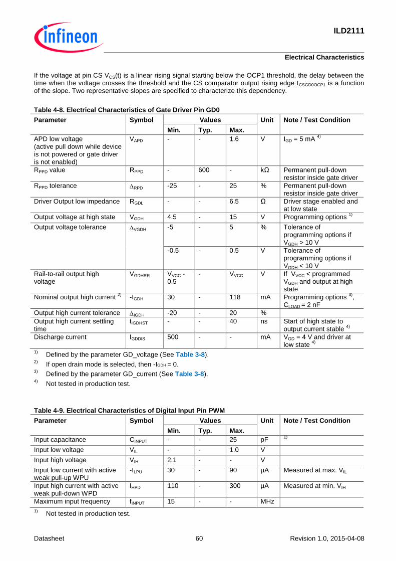
ILD2111
Electrical Characteristics
Datasheet 60 Revision 1.0, 2015-04-08
If the voltage at pin CS VCS(t) is a linear rising signal starting below the OCP1 threshold, the delay between the time when the voltage crosses the threshold and the CS comparator output rising edge tCSGD0OCP1 is a function of the slope. Two representative slopes are specified to characterize this dependency.
Table 4-8. Electrical Characteristics of Gate Driver Pin GD0
Parameter Symbol Values Unit Note / Test Condition
Min. Typ. Max.
APD low voltage (active pull down while device is not powered or gate driver is not enabled)
VAPD - - 1.6 V IGD = 5 mA 4)
RPPD value RPPD - 600 - kΩ Permanent pull-down resistor inside gate driver
RPPD tolerance RPD -25 - 25 % Permanent pull-down resistor inside gate driver
Driver Output low impedance RGDL - - 6.5 Ω Driver stage enabled and at low state
Output voltage at high state VGDH 4.5 - 15 V Programming options 1)
Output voltage tolerance VGDH -5 - 5 % Tolerance of programming options if VGDH > 10 V
-0.5 - 0.5 V Tolerance of programming options if VGDH < 10 V
Rail-to-rail output high voltage
VGDHRR VVCC - 0.5
- VVCC V If VVCC < programmed VGDH and output at high state
Nominal output high current 2)
-IGDH 30 - 118 mA Programming options 3)
, CLOAD = 2 nF
Output high current tolerance IGDH -20 - 20 %
Output high current settling time
tIGDHST - - 40 ns Start of high state to output current stable
4)
Discharge current IGDDIS 500 - - mA VGD = 4 V and driver at low state
4)
1) Defined by the parameter GD_voltage (See Table 3-8).
2) If open drain mode is selected, then -IGDH = 0.
3) Defined by the parameter GD_current (See Table 3-8).
4) Not tested in production test.
Table 4-9. Electrical Characteristics of Digital Input Pin PWM
Parameter Symbol Values Unit Note / Test Condition
Min. Typ. Max.
Input capacitance CINPUT - - 25 pF 1)
Input low voltage VIL - - 1.0 V
Input high voltage VIH 2.1 - - V
Input low current with active weak pull-up WPU
-ILPU 30 - 90 µA Measured at max. VIL
Input high current with active weak pull-down WPD
IHPD 110 - 300 µA Measured at min. VIH
Maximum input frequency fINPUT 15 - - MHz
1) Not tested in production test.

ILD2111
Electrical Characteristics
Datasheet 61 Revision 1.0, 2015-04-08
Table 4-10. Electrical Characteristics of Pin TS
Parameter Symbol Values Unit Note / Test Condition
Min. Typ. Max.
Nominal S&H input voltage range
VZSH 0 - 2/3 * VREF
V
Reduced S&H input voltage range
RRZVSH 4 - 95 % 2)
Maximum Error for ADC measurement (8 bit result)
TE0ZVS0 - - 6.3 LSB8 1)
TE256ZVS0 - - 6.3 LSB8 1)
Maximum Error for corrected ADC measurement (8 bit result)
TET0ZVS0 - - 2.8 LSB8 1)
TET256ZVS0 - - 4.6 LSB8 1)
S&H settling time for ADC sample
tZSHSTC - - 300 ns STC = 5
Voltage Drop of sampled input voltage if ADC measurement is started 100 μs after end of sampling phase
VZDROP 0 - 3 LSB8 TJ = 85°C 1)
0 5 - LSB8
TJ = 125°C 1)
1) Not tested in production test.
2) Operational values.
Table 4-11. Electrical Characteristics of the A/D Converter
1)
Parameter Symbol Values Unit Note / Test Condition
Min. Typ. Max.
Usable sample time tS 24 * tMCLK
- 64 * tMCLK
ns Selected by STC between 5 and 15
Conversion time for STC = 5 tC(STC=5) - 57 * tMCLK
- ns 2)
Conversion time for STC = 15 tC(STC=15) - 97 * tMCLK
- ns 2)
Integral non-linearity INL - - 1 LSB8 3)
Differential non-linearity DNL - - 0.8 LSB8
1) The sample time tS of the A/D converter is given by tS = (STC+1) * 4 * tMCLK. The conversion time tC
(including sample time) is given by tC = 33 * tMCLK + (STC+1) * 4 * tMCLK. 2)
Any conversion needs exact these numbers of clock cycles by design. 3)
ADC capability measured via channel MFIO without errors due to switching of neighboring pins, measured with STC = 5.
Table 4-12. Electrical Characteristics of the Reference Voltage VREF
Parameter Symbol Values Unit Note / Test Condition
Min. Typ. Max.
Reference voltage VREF - 2.428 - V
VREF tolerance VREF -1 - 1 % Trimmed, TA = 25°C
VREF tolerance VREF -2 - 2 % Trimmed, over full temperature range and aging
1)
1) Not tested in production test.

ILD2111
Electrical Characteristics
Datasheet 62 Revision 1.0, 2015-04-08
Table 4-13. Electrical Characteristics of the Clock Oscillators
Parameter Symbol Values Unit Note / Test Condition
Min. Typ. Max.
Master clock oscillation period
tMCLK 20.0 20.9 22.0 ns Referred as 50 MHz fMCLK
Table 4-14. Electrical Characteristics of the internal Temperature Sensor
Parameter Symbol Values Unit Note / Test Condition
Min. Typ. Max.
Temperature sensor output voltage operating range
VADCTEMP 0 - 190/255 * VREF
V VADCTEMP = VREF/255 * (40 + temperature in °C)
Temperature sensor tolerance
TEMP -8 - 8 K Incl. ADC conversion accuracy at 4 σ
1)
1) Not tested in production test.
Table 4-15. Electrical Characteristics of the OTP Programming
Parameter Symbol Values Unit Note / Test Condition
Min. Typ. Max.
OTP programming voltage at the VCC pin
VPP 7.35 7.5 7.65 V 1) 2)
OTP programming current IPP - 1.6 - mA Programming of 4 bit in parallel
2)
1) Operational values.
2) Not tested in production test.

ILD2111
Outline Dimensions
Datasheet 63 Revision 1.0, 2015-04-08
5 Outline Dimensions
Outline dimensions are shown in Figure 32.
Figure 32. PG-DSO-8-58
Notes 1. You can find all of our packages, types of packing and other information on our Infineon Internet page “Products”:
http://www.infineon.com/products.
2. Dimensions in mm.

Edition 2015-04-08
Published by Infineon Technologies AG 81726 Munich, Germany
© 2015 Infineon Technologies AG All Rights Reserved.
Legal Disclaimer
The information given in this document shall in no event be regarded as a guarantee of conditions or characteristics. With respect to any examples or hints given herein, any typical values stated herein and/or any information regarding the application of the device, Infineon Technologies hereby disclaims any and all warranties and liabilities of any kind, including without limitation, warranties of non-infringement of intellectual property rights of any third party.
Information
For further information on technology, delivery terms and conditions and prices, please contact the nearest Infineon Technologies Office (www.infineon.com).
Warnings
Due to technical requirements, components may contain dangerous substances. For information on the types in question, please contact the nearest Infineon Technologies Office.
Infineon Technologies components may be used in life-support devices or systems only with the express written approval of Infineon Technologies, if a failure of such components can reasonably be expected to cause the failure of that life-support device or system or to affect the safety or effectiveness of that device or system. Life support devices or systems are intended to be implanted in the human body or to support and/or maintain and sustain and/or protect human life. If they fail, it is reasonable to assume that the health of the user or other persons may be endangered.
ILD2111
Revision History: 2015-04-08, Revision 1.0
Previous Revision: None (initial version)
Page or Item Subjects (major changes since previous revision)
Trademarks of Infineon Technologies AG
AURIX™, C166™, CanPAK™, CIPOS™, CIPURSE™, EconoPACK™, CoolMOS™, CoolSET™, CORECONTROL™, CROSSAVE™, DAVE™, DI-POL™, EasyPIM™, EconoBRIDGE™, EconoDUAL™, EconoPIM™, EconoPACK™, EiceDRIVER™, eupec™, FCOS™, HITFET™, HybridPACK™, I²RF™, ISOFACE™, IsoPACK™, MIPAQ™, ModSTACK™, my-d™, NovalithIC™, OptiMOS™, ORIGA™, POWERCODE™, PRIMARION™, PrimePACK™, PrimeSTACK™, PRO-SIL™, PROFET™, RASIC™, ReverSave™, SatRIC™, SIEGET™, SINDRION™, SIPMOS™, SmartLEWIS™, SOLID FLASH™, TEMPFET™, thinQ!™, TRENCHSTOP™, TriCore™.
Other Trademarks
Advance Design System™ (ADS) of Agilent Technologies, AMBA™, ARM™, MULTI-ICE™, KEIL™, PRIMECELL™, REALVIEW™, THUMB™, µVision™ of ARM Limited, UK. AUTOSAR™ is licensed by AUTOSAR development partnership. Bluetooth™ of Bluetooth SIG Inc. CAT-iq™ of DECT Forum. COLOSSUS™, FirstGPS™ of Trimble Navigation Ltd. EMV™ of EMVCo, LLC (Visa Holdings Inc.). EPCOS™ of Epcos AG. FLEXGO™ of Microsoft Corporation. FlexRay™ is licensed by FlexRay Consortium. HYPERTERMINAL™ of Hilgraeve Incorporated. IEC™ of Commission Electrotechnique Internationale. IrDA™ of Infrared Data Association Corporation. ISO™ of INTERNATIONAL ORGANIZATION FOR STANDARDIZATION. MATLAB™ of MathWorks, Inc. MAXIM™ of Maxim Integrated Products, Inc. MICROTEC™, NUCLEUS™ of Mentor Graphics Corporation. MIPI™ of MIPI Alliance, Inc. MIPS™ of MIPS Technologies, Inc., USA. muRata™ of MURATA MANUFACTURING CO., MICROWAVE OFFICE™ (MWO) of Applied Wave Research Inc., OmniVision™ of OmniVision Technologies, Inc. Openwave™ Openwave Systems Inc. RED HAT™ Red Hat, Inc. RFMD™ RF Micro Devices, Inc. SIRIUS™ of Sirius Satellite Radio Inc. SOLARIS™ of Sun Microsystems, Inc. SPANSION™ of Spansion LLC Ltd. Symbian™ of Symbian Software Limited. TAIYO YUDEN™ of Taiyo Yuden Co. TEAKLITE™ of CEVA, Inc. TEKTRONIX™ of Tektronix Inc. TOKO™ of TOKO KABUSHIKI KAISHA TA. UNIX™ of X/Open Company Limited. VERILOG™, PALLADIUM™ of Cadence Design Systems, Inc. VLYNQ™ of Texas Instruments Incorporated. VXWORKS™, WIND RIVER™ of WIND RIVER SYSTEMS, INC. ZETEX™ of Diodes Zetex Limited.
Last Trademarks Update 2011-11-11

w w w . i n f i n e o n . c o m
Published by Infineon Technologies AG