imm4g72d3(l)lrq4ag (die revision d) 32gbyte (4096m x 72 bit)
TRANSCRIPT
www.intelligentmemory.com 1 IMM4G72D3(L)LRQ4AG
We Listen to Your Comments
Any information within this document that you feel is wrong, unclear or missing at all? Your feedback will help us to continuously improve the quality of this document. Please send your proposal (including a reference to this document) to: [email protected]
Datasheet | Rev. 1.0 | 2021
IMM4G72D3(L)LRQ4AG (Die Revision D) 32GByte (4096M x 72 Bit) 32GB DDR3 Load Reduced DIMM RoHS Compliant Product
Remark: Please refer to the last page of the i) Contents ii) List of Table iii) List of Figures.

www.intelligentmemory.com 2 IMM4G72D3(L)LRQ4AG
Features
240-Pin Load Reduced Dual-In-Line Memory Module Capacity: 32GB Memory Buffer JEDEC-Standard Bi-directional Differential Data-Strobe 72 Bit Data Bus Width with ECC Programmable CAS Latency (CL):
o PC3-12800: 5, 6, 7, 8, 9, 10, 11 o PC3-10600: 5, 6, 7, 8, 9, 10
Programmable CAS Write Latency (CWL): o PC3-12800: 5, 6, 7, 8 o PC3-10600: 5, 6, 7
Programmable Additive Latency (Posted /CAS): 0, CL-2 or CL-1(Clock) On-Die Termination (ODT) ZQ Calibration Supported Burst Type (Sequential & Interleave) Burst Length: 4, 8 Refresh Mode: Auto and Self 8192 Refresh Cycles / 64ms Asynchronous Reset On-board I2C Temperature Sensor with Integrated Serial Presence Detect (SPD)
EEPROM Gold Edge Contacts 100% RoHS-Compliant Standard Module Height: 30.35mm (1.195 inch)
www.intelligentmemory.com 3 IMM4G72D3(L)LRQ4AG
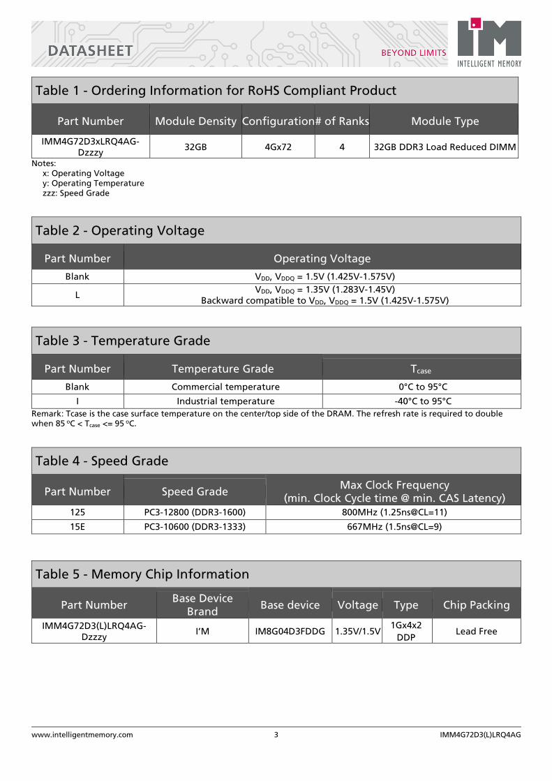
Table 1 - Ordering Information for RoHS Compliant Product
Part Number Module Density Configuration# of Ranks Module Type
IMM4G72D3xLRQ4AG-Dzzzy
32GB 4Gx72 4 32GB DDR3 Load Reduced DIMM
Notes: x: Operating Voltage y: Operating Temperature zzz: Speed Grade
Table 2 - Operating Voltage
Part Number Operating Voltage
Blank VDD, VDDQ = 1.5V (1.425V-1.575V)
L VDD, VDDQ = 1.35V (1.283V-1.45V)
Backward compatible to VDD, VDDQ = 1.5V (1.425V-1.575V)
Remark: Tcase is the case surface temperature on the center/top side of the DRAM. The refresh rate is required to double when 85 oC < Tcase <= 95 oC.
Table 4 - Speed Grade
Part Number Speed Grade Max Clock Frequency
(min. Clock Cycle time @ min. CAS Latency) 125 PC3-12800 (DDR3-1600) 800MHz (1.25ns@CL=11)
15E PC3-10600 (DDR3-1333) 667MHz (1.5ns@CL=9)
Table 5 - Memory Chip Information
Part Number Base Device
Brand Base device Voltage Type Chip Packing
IMM4G72D3(L)LRQ4AG-Dzzzy
I’M IM8G04D3FDDG 1.35V/1.5V 1Gx4x2
DDP Lead Free
Table 3 - Temperature Grade
Part Number Temperature Grade Tcase
Blank Commercial temperature 0°C to 95°C
I Industrial temperature -40°C to 95°C
www.intelligentmemory.com 4 IMM4G72D3(L)LRQ4AG
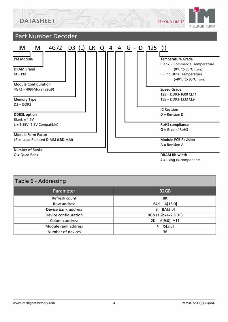
Part Number Decoder
IM M 4G72 D3 (L) LR Q 4 A G - D 125 (I)
I'M Module Temperature Grade
Blank = Commercial Temperature
DRAM Brand (0°C to 95°C Tcase)
M = I'M I = Industrial Temperature
(-40°C to 95°C Tcase)
Module Configuration
4G72 = 4096Mx72 (32GB) Speed Grade
125 = DDR3-1600 CL11
Memory Type 15E = DDR3-1333 CL9
D3 = DDR3
IC Revision
DDR3L option D = Revision D
Blank = 1.5V
L = 1.35V (1.5V Compatible) RoHS compliance
G = Green / RoHS
Module Form-Factor
LR = Load Reduced DIMM (LRDIMM) Module PCB Revision
A = Revision A
Number of Ranks
Q = Quad Rank DRAM Bit width
4 = using x4 components
Table 6 - Addressing
Parameter 32GB
Refresh count 8K
Row address 64K A[15:0]
Device bank address 8 BA[2:0]
Device configuration 8Gb (1Gbx4x2 DDP)
Column address 2K A[9:0], A11
Module rank address 4 /S[3:0]
Number of devices 36

www.intelligentmemory.com 5 IMM4G72D3(L)LRQ4AG
Table 7 - Pin Assignment
Pin Name Pin Name Pin Name Pin Name 1 VREFDQ 121 VSS 61 A2 181 A1
2 VSS 122 D4 62 VDD 182 VDD
3 D0 123 D5 63 CK1 183 VDD
4 D1 124 VSS 64 /CK1 184 CK0
5 VSS 125 DQS9 65 VDD 185 /CK0
6 /DQS0 126 /DQS9 66 VDD 186 VDD
7 DQS0 127 VSS 67 VREFCA 187 /EVENT
8 VSS 128 D6 68 PAR_IN 188 A0
9 D2 129 D7 69 VDD 189 VDD
10 D3 130 VSS 70 A10, AP 190 BA1
11 VSS 131 D12 71 BA0 191 VDD
12 D8 132 D13 72 VDD 192 /RAS
13 D9 133 VSS 73 /WE 193 /S0
14 VSS 134 DQS10 74 /CAS 194 VDD
15 /DQS1 135 /DQS10 75 VDD 195 ODT0
16 DQS1 136 VSS 76 /S1 196 A13
17 VSS 137 D14 77 ODT1, CKE3 197 VDD
18 D10 138 D15 78 VDD 198 /S3
19 D11 139 VSS 79 /S2 199 VSS
20 VSS 140 D20 80 VSS 200 D36
21 D16 141 D21 81 D32 201 D37
22 D17 142 VSS 82 D33 202 VSS
23 VSS 143 DQS11 83 VSS 203 DQS13
24 /DQS2 144 /DQS11 84 /DQS4 204 /DQS13
25 DQS2 145 VSS 85 DQS4 205 VSS
26 VSS 146 D22 86 VSS 206 D38
27 D18 147 D23 87 D34 207 D39
28 D19 148 VSS 88 D35 208 VSS
29 VSS 149 D28 89 VSS 209 D44
30 D24 150 D29 90 D40 210 D45
31 D25 151 VSS 91 D41 211 VSS
32 VSS 152 DQS12 92 VSS 212 DQS14
33 /DQS3 153 /DQS12 93 /DQS5 213 /DQS14
34 DQS3 154 VSS 94 DQS5 214 VSS
35 VSS 155 D30 95 VSS 215 D46
36 D26 156 D31 96 D42 216 D47
37 D27 157 VSS 97 D43 217 VSS
38 VSS 158 CB4 98 VSS 218 D52
39 CB0 159 CB5 99 D48 219 D53
40 CB1 160 VSS 100 D49 220 VSS
41 VSS 161 DQS17 101 VSS 221 DQS15
42 /DQS8 162 /DQS17 102 /DQS6 222 /DQS15
43 DQS8 163 VSS 103 DQS6 223 VSS
44 VSS 164 CB6 104 VSS 224 D54
45 CB2 165 CB7 105 D50 225 D55
46 CB3 166 VSS 106 D51 226 VSS
47 VSS 167 CKE2 107 VSS 227 D60
48 VTT 168 /RESET 108 D56 228 D61
49 VTT 169 CKE1 109 D57 229 VSS
50 CKE0 170 VDD 110 VSS 230 DQS16
51 VDD 171 A15 111 /DQS7 231 /DQS16
52 BA2 172 A14 112 DQS7 232 VSS
53 /ERR_OUT 173 VDD 113 VSS 233 D62
54 VDD 174 A12, /BC 114 D58 234 D63
55 A11 175 A9 115 D59 235 VSS
56 A7 176 VDD 116 VSS 236 VDDSPD
57 VDD 177 A8 117 SA0 237 SA1
58 A5 178 A6 118 SCL 238 SDA
59 A4 179 VDD 119 SA2 239 VSS
60 VDD 180 A3 120 VTT 240 VTT
www.intelligentmemory.com 6 IMM4G72D3(L)LRQ4AG
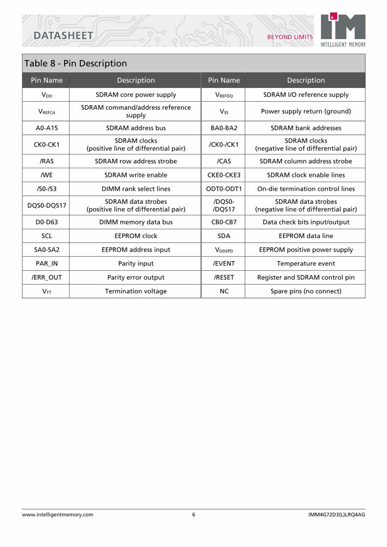
Table 8 - Pin Description
Pin Name Description Pin Name Description
VDD SDRAM core power supply VREFDQ SDRAM I/O reference supply
VREFCA SDRAM command/address reference
supply VSS Power supply return (ground)
A0-A15 SDRAM address bus BA0-BA2 SDRAM bank addresses
CK0-CK1 SDRAM clocks
(positive line of differential pair) /CK0-/CK1
SDRAM clocks (negative line of differential pair)
/RAS SDRAM row address strobe /CAS SDRAM column address strobe
/WE SDRAM write enable CKE0-CKE3 SDRAM clock enable lines
/S0-/S3 DIMM rank select lines ODT0-ODT1 On-die termination control lines
DQS0-DQS17 SDRAM data strobes
(positive line of differential pair) /DQS0-/DQS17
SDRAM data strobes (negative line of differential pair)
D0-D63 DIMM memory data bus CB0-CB7 Data check bits input/output
SCL EEPROM clock SDA EEPROM data line
SA0-SA2 EEPROM address input VDDSPD EEPROM positive power supply
PAR_IN Parity input /EVENT Temperature event
/ERR_OUT Parity error output /RESET Register and SDRAM control pin
VTT Termination voltage NC Spare pins (no connect)

www.intelligentmemory.com 7 IMM4G72D3(L)LRQ4AG
Module Dimension
Figure 1 - 240 Pin DDR3 SDRAM Load Reduced DIMM
Table 9 - PCB Dimension
Symbol MIN NOM MAX
A 30.20 30.35 30.50
A1 9.50 Basic
A2 4.00
A3 17.30 Basic
A4 23.30 Basic
D 133.20 133.35 133.50
D1 128.95 Basic
D2 2.50 Basic
D3 12.00 Basic
e1 47.00 Basic
e2 71.00 Basic
E 4.80
Notes: All dimensioning and tolerancing conform to ASME Y14.5M-1994. Tolerances for all dimensions ±0.15 unless otherwise specified. All dimensions are in millimeters.

www.intelligentmemory.com 8 IMM4G72D3(L)LRQ4AG
Figure 2 - Functional Block Diagram (Page 1 of 6)

www.intelligentmemory.com 9 IMM4G72D3(L)LRQ4AG
Figure 3 - Functional Block Diagram (Page 2 of 6)

www.intelligentmemory.com 10 IMM4G72D3(L)LRQ4AG
Figure 4 - Functional Block Diagram (Page 3 of 6)

www.intelligentmemory.com 11 IMM4G72D3(L)LRQ4AG
Figure 5 - Functional Block Diagram (Page 4 of 6)
www.intelligentmemory.com 12 IMM4G72D3(L)LRQ4AG
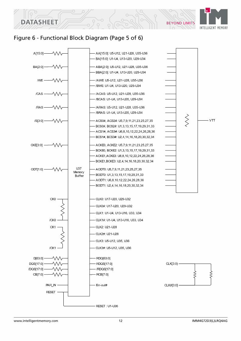
Figure 6 - Functional Block Diagram (Page 5 of 6)

www.intelligentmemory.com 13 IMM4G72D3(L)LRQ4AG
Figure 7 - Functional Block Diagram (Page 6 of 6)

www.intelligentmemory.com 14 IMM4G72D3(L)LRQ4AG
Electrical Parameter
Table 10 - Absolute Maximum DC Ratings
Parameter Symbol Rating Unit Notes
Voltage on VDD, pin relative to VSS VDD -0.4V ~ 1.975 V 1,3
Voltage on VDDQ, pin relative to VSS VDDQ -0.4V ~ 1.975 V 1,3
Voltage on any pins relative to VSS VIN, VOUT -0.4V ~ 1.975 V 1
DRAM Storage temperature TSTG -55 ~ 100 oC 1,2
DRAM Operation temperature for Commercial temperature product
Tcase 0 ~ 95 oC 2,4,5
DRAM Operation temperature for Industrial temperature product
Tcase -40 ~ 95 oC 2,4,5
Notes: 1 Stresses greater than those listed under “Absolute Maximum Ratings” may cause permanent damage to the device. This is
a stress rating only and functional operation of the device at these or any other conditions above those indicated in the operational sections of this specification is not implied. Exposure to absolute maximum rating conditions for extended periods may affect reliability.
2 Storage Temperature or DRAM operation temperature is the case surface temperature on the center/top side of the DRAM.
For the measurement conditions, please refer to JESD51-2 standard. 3 VDD and VDDQ must be within 300mV of each other at all times; and VREF must not be greater than 0.6 x VDDQ, when VDD and
VDDQ are less than 500mV; VREF may be equal to or less than 300mV. 4 The Normal Temperature Range specifies the temperatures when all DRAM specifications will be supported. During
operation, the DRAM case temperature must be maintained between 0-85 °C under all operating conditions. 5 Some applications require operation of the Extended Temperature Range between 85 °C and 95 °C case temperature. Full
Specifications are guaranteed in this range but the following additional conditions apply a) Refresh commands must be doubled in frequency, therefore reducing the refresh interval tREFI to 3.9us. b) If Self-Refresh operation is required in the Extended Temperature Range, then it is mandatory to either use the Manual Self-Refresh mode with Extended Temperature Range capability (MR2 A6 = 0b and MR2 A7 = 1b) or enable the optional Auto Self-Refresh mode (MR2 A6 = 1b and MR2 A7 = 0b).
Table 11 - DC Electrical Characteristics and Operating Conditions
Parameter / Condition Symbol Rating
Units Notes Min Typ Max
Supply voltage VDD 1.283 1.35 1.45
V 1,2 I/O supply voltage VDDQ V 1,2 Supply voltage VDD
1.425 1.5 1.575 V 1,2,3
I/O supply voltage VDDQ V 1,2,3 Notes: 1. VDD and VDDQ must track one another. VDDQ must be less than or equal to VDD. VSS = VSSQ.
2. VDD and VDDQ may include AC noise of +/-50mV (250 kHz to 20 MHz) in addition to the DC (0 Hz to 250 kHz) specifications.
VDD and VDDQ must be at same level for valid AC timing parameters. 3. Module is backward-compatible with 1.5V operation.

www.intelligentmemory.com 15 IMM4G72D3(L)LRQ4AG
Table 12 - DC Electrical Characteristics and Input Conditions
Parameter / Condition Symbol Rating
Units Notes Min Typ Max
VIN low; DC/commands/address buses (1.35V) VIL VSS - VREF - 0.090 V VIN low; DC/commands/address buses (1.5V) VIL VSS - VREF - 0.100 V VIN high; DC/commands/address buses (1.35V)
VIH VREF + 0.090 - VDD V
VIN high; DC/commands/address buses (1.5V) VIH VREF + 0.100 - VDD V Input reference voltage; command/address bus
VREFCA(DC) 0.49* VDD 0.50* VDD 0.51* VDD V 1,2
I/O reference voltage DQ bus VREFDQ(DC) 0.49* VDD 0.50* VDD 0.51* VDD V 2,3 Command/address termination voltage (system level, not direct DRAM input)
VTT - 0.50* VDDQ - V 4
Notes: 1. VREFCA(DC) is expected to be approximately 0.5 × VDD and to track variations in the DC level. Externally generated peak noise
(noncommon mode) on VREFCA may not exceed ±1% × VDD around the VREFCA(DC) value. Peak-to-peak AC noise on VREFCA should not exceed ±2% of VREFCA(DC).
2. DC values are determined to be less than 20 MHz in frequency. DRAM must meet specifications if the DRAM induces additional AC noise greater than 20 MHz in frequency.
3. VREFDQ(DC) is expected to be approximately 0.5 × VDD and to track variations in the DC level. Externally generated peak noise (noncommon mode) on VREFDQ may not exceed ±1% × VDD around the VREFDQ(DC) value. Peak-to-peak AC noise on VREFDQ should not exceed ±2% of VREFDQ(DC).
4. VTT is not applied directly to the device. VTT is a system supply for signal termination resistors. MIN and MAX values are system-dependent.

www.intelligentmemory.com 16 IMM4G72D3(L)LRQ4AG
Table 13 - Input Switching Conditions
Parameter / Condition Symbol Value
Units 1.35V 1.5V
Command and Address Input high AC voltage: Logic 1 @ 175mV DDR3-1600, 1333 VIH(AC175)min - 175 mV Input high AC voltage: Logic 1 @ 160mV DDR3-1600, 1333 VIH(AC160)min 160 - mV Input high AC voltage: Logic 1 @ 150mV DDR3-1600, 1333 VIH(AC150)min - 150 mV Input high AC voltage: Logic 1 @ 135mV DDR3-1600, 1333 VIH(AC135)min 135 - mV Input high DC voltage: Logic 1 @ 100mV DDR3-1600, 1333 VIH(DC100)min - 100 mV Input high DC voltage: Logic 1 @ 90mV DDR3-1600, 1333 VIH(DC90)min 90 - mV Input low DC voltage: Logic 0 @ -90mV DDR3-1600, 1333 VIL(DC90)max -90 - mV Input low DC voltage: Logic 0 @ -100mV DDR3-1600, 1333 VIL(DC100)max - -100 mV Input low AC voltage: Logic 0 @ -135mV DDR3-1600, 1333 VIL(AC135)max -135 - mV Input low AC voltage: Logic 0 @ -150mV DDR3-1600, 1333 VIL(AC150)max - -150 mV Input low AC voltage: Logic 0 @ -160mV DDR3-1600, 1333 VIL(AC160)max -160 - mV Input low AC voltage: Logic 0 @ -175mV DDR3-1600, 1333 VIL(AC175)max - -175 mV
Parameter / Condition Symbol Value
Units 1.35V 1.5V
DQ and DM Input high AC voltage: Logic 1 DDR3-1600, 1333 VIH(AC150)min - 150 mV Input high AC voltage: Logic 1 DDR3-1600, 1333 VIH(AC135)min 135 135 mV Input high DC voltage: Logic 1 DDR3-1600, 1333 VIH(DC100)min - 100 mV Input high DC voltage: Logic 1 DDR3-1600, 1333 VIH(DC90)min 90 - mV Input low DC voltage: Logic 0 DDR3-1600, 1333 VIL(DC90)max -90 - mV Input low DC voltage: Logic 0 DDR3-1600, 1333 VIL(DC100)max - -100 mV Input low AC voltage: Logic 0 DDR3-1600, 1333 VIL(AC135)max -135 -135 mV Input low AC voltage: Logic 0 DDR3-1600, 1333 VIL(AC150)max - -150 mV
Notes: 1. All voltages are referenced to VREF. VREF is VREFCA for control, command, and address. All slew rates and setup/hold times
are specified at the DRAM ball. VREF is VREFDQ for DQ and DM inputs. 2. Input setup timing parameters (tIS and tDS) are referenced at VIL(AC)/VIH(AC), not VREF(DC). 3. Input hold timing parameters (tIH and tDH) are referenced at VIL(DC)/VIH(DC), not VREF(DC). 4. Single-ended input slew rate = 1 V/ns; maximum input voltage swing under test is 900mV (peak-to-peak).

www.intelligentmemory.com 17 IMM4G72D3(L)LRQ4AG
Table 14 - Differential Input Operating Conditions (CK, /CK and DQS, /DQS)
Parameter / Condition Symbol Rating
Units Notes Min Max
Differential input voltage logic high - slew (1.35V) VIH,diff +180 - mV 1 Differential input voltage logic high - slew (1.5V) VIH,diff +200 - mV 1 Differential input voltage logic low - slew (1.35V) VIL,diff - -180 mV 1 Differential input voltage logic low - slew (1.5V) VIL,diff - -200 mV 1 Differential input voltage logic high VIH,diff(AC) 2* (VIH(AC) - VREF) - mV 2 Differential input voltage logic low VIL,diff(AC) - 2* (VIL(AC) - VREF) mV 3 Single-ended high level for strobes
VSEH VDDQ/2 + 175 - mV 2
Single-ended high level for CK, /CK VDD/2 + 175 - mV 2 Single-ended low level for strobes
VSEL - VDDQ/2 - 175 mV 3
Single-ended low level for CK, /CK - VDD/2 - 175 mV 3 Notes: 1. Defines slew rate reference points, relative to input crossing voltages. 2. Minimum DC limit is relative to single-ended signals; overshoot specifications are applicable. 3. Maximum DC limit is relative to single-ended signals; undershoot specifications are applicable.
Table 15 - Single-Ended Output Driver Characteristics
Parameter / Condition Symbol Rating
Units Notes Min Max
Output slew rate: Single-ended; For rising and falling edges, measure between VOL(AC) = VTT - 0.1 * VDDQ and VOH(AC) = VTT + 0.1 * VDDQ (1.35V)
SRQse 1.75 5 V/ns 1,2,3
Output slew rate: Single-ended; For rising and falling edges, measure between VOL(AC) = VTT - 0.1 * VDDQ and VOH(AC) = VTT + 0.1 * VDDQ (1.5V)
SRQse 2.5 5 V/ns 1,2,3
Single-ended DC high-level output voltage VOH(DC) 0.8 * VDDQ V 1,2 Single-ended DC mid-level output voltage VOM(DC) 0.5 * VDDQ V 1,2 Single-ended DC low-level output voltage VOL(DC) 0.2 * VDDQ V 1,2 Single-ended AC high-level output voltage VOH(AC) VTT + 0.1 * VDDQ V 1,2 Single-ended AC low-level output voltage VOL(AC) VTT - 0.1 * VDDQ V 1,2 Test load for AC timing and output slew rates Output to VTT (VDDQ/2) via 25Ω resistor
Notes: 1. RZQ of 240Ω (±1%) with RZQ/7 enabled (default 34Ω driver) and is applicable after proper ZQ calibration has been
performed at a stable temperature and voltage (VDDQ = VDD, VSSQ = VSS). 2. VTT = VDDQ/2. 3. The 6 V/ns maximum is applicable for a single DQ signal when it is switching either from HIGH to LOW or LOW to HIGH
while the remaining DQ signals in the same byte lane are either all static or all switching the opposite direction. For all other DQ signal switching combinations, the maximum limit of 6 V/ns is reduced to 5 V/ns.

www.intelligentmemory.com 18 IMM4G72D3(L)LRQ4AG
Table 16 - Differential Output Driver Characteristics
Parameter / Condition Symbol Rating
Units Notes Min Max
Output slew rate: Differential; For rising and falling edges, measure between VOL,diff(AC), = - 0.2 * VDDQ and VOH,diff(AC) = + 0.2 * VDDQ (1.35V)
SRQdiff 3.5 12 V/ns 1
Output slew rate: Differential; For rising and falling edges, measure between VOL,diff(AC), = - 0.2 * VDDQ and VOH,diff(AC) = + 0.2 * VDDQ (1.5V)
SRQdiff 5 10 V/ns 1
Differential high-level output voltage VOH,diff(AC) +0.2 * VDDQ V 1 Differential low-level output voltage VOL,diff(AC) -0.2 * VDDQ V 1 Test load for AC timing and output slew rates Output to VTT (VDDQ/2) via 25Ω resistor
Notes: 1.
RZQ of 240Ω (±1%) with RZQ/7 enabled (default 34Ω driver) and is applicable after proper ZQ calibration has been performed at a stable temperature and voltage (VDDQ = VDD, VSSQ = VSS).
2. VREF = VDDQ/2; slew rate @ 5V/ns, interpolate for faster slew rate.
www.intelligentmemory.com 19 IMM4G72D3(L)LRQ4AG
For part number IMM4G72D3(L)LRQ4AG-D125(I)
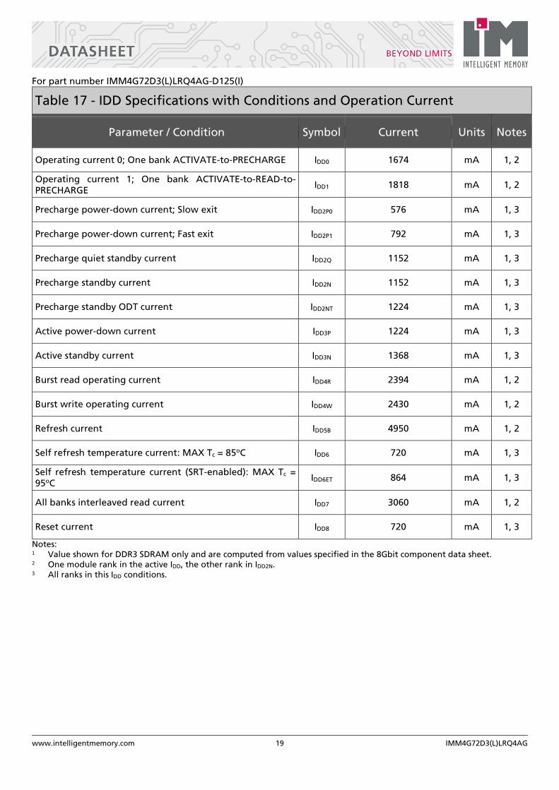
Table 17 - IDD Specifications with Conditions and Operation Current
Parameter / Condition Symbol Current Units Notes
Operating current 0; One bank ACTIVATE-to-PRECHARGE IDD0 1674 mA 1, 2
Operating current 1; One bank ACTIVATE-to-READ-to-PRECHARGE
IDD1 1818 mA 1, 2
Precharge power-down current; Slow exit IDD2P0 576 mA 1, 3
Precharge power-down current; Fast exit IDD2P1 792 mA 1, 3
Precharge quiet standby current IDD2Q 1152 mA 1, 3
Precharge standby current IDD2N 1152 mA 1, 3
Precharge standby ODT current IDD2NT 1224 mA 1, 3
Active power-down current IDD3P 1224 mA 1, 3
Active standby current IDD3N 1368 mA 1, 3
Burst read operating current IDD4R 2394 mA 1, 2
Burst write operating current IDD4W 2430 mA 1, 2
Refresh current IDD5B 4950 mA 1, 2
Self refresh temperature current: MAX Tc = 85oC IDD6 720 mA 1, 3
Self refresh temperature current (SRT-enabled): MAX Tc = 95oC
IDD6ET 864 mA 1, 3
All banks interleaved read current IDD7 3060 mA 1, 2
Reset current IDD8 720 mA 1, 3
Notes: 1 Value shown for DDR3 SDRAM only and are computed from values specified in the 8Gbit component data sheet. 2 One module rank in the active IDD, the other rank in IDD2N. 3 All ranks in this IDD conditions.

www.intelligentmemory.com 20 IMM4G72D3(L)LRQ4AG
For part number IMM4G72D3(L)LRQ4AG-D125(I)
Table 18 - AC Timing Parameter and Operating Conditions
Parameter / Condition Symbol Min Max Units Clock Timing
Clock period average: DLL disable mode
TC = 0oC to 85oC tCK(DLL_DIS)
8 - ns
TC => 85oC to 95oC 8 -
Clock periods average: DLL enable mode (CL = 11, CWL = 8) tCK(avg) 1.25 1.5 ns
Clock periods average: DLL enable mode (CL = 9, CWL = 7) tCK(avg) 1.5 1.875 ns
High pulse width average tCH(avg) 0.47 0.53 tCK(avg)
Low pulse width average tCL(avg) 0.47 0.53 tCK(avg)
Clock period jitter DLL locked tJITper 70 70 ps
DLL locking tJIT(per,Ick) -60 60 ps
Clock absolute period tCK(abs) tCK(avg) Min +
tJITper Min tCK(avg) Max +
tJITper Max ps
Clock absolute high pulse width tCH(abs) 0.43 - tCK(avg)
Clock absolute low pulse width tCL(abs) 0.43 - tCK(avg)
Cycle-to-cycle jitter DLL locked tJITcc - 140 ps
DLL locking tJIT(cc,Ick) - 120 ps
Cumulative error across
2 cycles tERR(2per) -103 103 ps
3 cycles tERR(3per) -122 122 ps
4 cycles tERR(4per) -136 136 ps
5 cycles tERR(5per) -147 147 ps
6 cycles tERR(6per) -155 155 ps
7 cycles tERR(7per) -163 163 ps
8 cycles tERR(8per) -169 169 ps
9 cycles tERR(9per) -175 175 ps
10 cycles tERR(10per) -180 180 ps
11 cycles tERR(11per) -174 174 ps
12 cycles tERR(12per) -188 188 ps
n = 13,…49, 50 cycles tERR(nper) (1+0.68ln[n]) *
tJITper Min (1+0.68ln[n]) *
tJITper Max ps
DQ Input Timing
Data setup time to DQS, /DQS (1.35V) Base (specification) tDS(AC130) 25 - ps
Data setup time to DQS, /DQS (1.5V) Base (specification) tDS(AC135) 10 - ps
Data hold time from DQS, /DQS (1.35V)
Base (specification) tDH(DC90) 55 - ps
Data hold time from DQS, /DQS (1.5V) Base (specification) tDH(DC100) 45 - ps
Minimum data pulse width tDIPW 360 - ps
DQ Output Timing
DQS, /DQS to DQ skew, per access tDQSQ - 85 ps
DQ output hold time from DQS, /DQS tQH 0.38 - tCK(avg)
DQ Low-Z time from CK, /CK tLZ(DQ) -390 195 ps
DQ High-Z time from CK, /CK tHZ(DQ) - 195 ps
DQ Strobe Input Timing
DQS, /DQS rising to CK, /CK rising tDQSS -0.27 0.27 tCK(avg)
DQS, /DQS differential input low pulse width tDQSL 0.45 0.55 tCK(avg)
DQS, /DQS falling setup to CK, /CK rising tDSS 0.18 - tCK(avg))
DQS, /DQS falling hold from CK, /CK rising tDSH 0.18 - tCK(avg)
DQS, /DQS differential input high pulse width tDQSH 0.45 0.55 tCK(avg)
DQS, /DQS differential WRITE preamble tWPRE 0.9 - tCK(avg)
DQS, /DQS differential WRITE postamble tWPST 0.3 - tCK(avg)

www.intelligentmemory.com 21 IMM4G72D3(L)LRQ4AG
For part number IMM4G72D3(L)LRQ4AG-D125(I)
Parameter / Condition Symbol Min Max Units DQ Strobe Output Timing
DQS, /DQS rising to/from CK, /CK tDQSCK -225 225 ps
DQS, /DQS differential output high time tQSH 0.45 - tCK(avg)
DQS, /DQS differential output low time tQSL 0.45 - tCK(avg)
DQS, /DQS Low-Z time (RL-1) tLZ(DQS) -450 225 ps
DQS, /DQS High-Z time (RL+BL/2) tHZ(DQS) - 225 ps
DQS, /DQS differential READ preamble tRPRE 0.9 tCK(avg)
DQS, /DQS differential READ postamble tRPST 0.3 tCK(avg)
Command and Address Timing
DLL locking time tDLLK 512 - nCK
CTRL, CMD, ADDR setup to CK, /CK (1.35V)
Base (specification) tIS(AC160) 60 - ps
CTRL, CMD, ADDR setup to CK, /CK (1.35V)
Base (specification) tIS(AC135) 185 - ps
CTRL, CMD, ADDR setup to CK, /CK (1.5V)
Base (specification) tIS(AC175) 170 - ps
CTRL, CMD, ADDR setup to CK, /CK (1.5V)
Base (specification) tIS(AC150) 120 - ps
CTRL, CMD, ADDR hold from CK, /CK (1.35V)
Base (specification) tIH(DC90) 130 - ps
CTRL, CMD, ADDR hold from CK, /CK (1.5V)
Base (specification) tIH(DC100) 120 - ps
Minimum CTRL, CMD, ADDR pulse width tIPW 560 - ps
ACTIVATE to internal READ or WRITE delay tRCD 13.125 - ns
PRECHARGE command period tRP 13.125 - ns
ACTIVATE-to-PRECHARGE command period tRAS 35 9 * tREFI ns
ACTIVATE-to-ACTIVATE command period tRC 48.125 - ns
ACTIVATE-to-ACTIVATE minimum period (1KB page size) tRRD greater of 4nCK or
6ns - -
ACTIVATE-to-ACTIVATE minimum period (2KB page size) tRRD greater of 4nCK or
7.5ns - -
Four ACTIVATE windows (1KB page size) tFAW 30 - ns
Four ACTIVATE windows (2KB page size) tFAW 40 - ns
Write recovery time tWR 15 - ns
Delay from start of internal WRITE transaction to internal READ command
tWTR greater of 4nCK or
7.5ns - -
READ-to-PRECHARGE time tRTP greater of 4nCK or
7.5ns - -
/CAS-to-/CAS command delay tCCD 4 - tCK
Auto precharge write recovery + precharge time tDAL WR + tRP/ tCK(avg) - tCK
MODE REGISTER SET command cycle time tMRD 4 - nCK
MODE REGISTER SET command update delay tMOD greater of 12nCK
or 15ns - -
MULTIPURPOSE REGISTER READ burst end to mode register set for multipurpose register exit
tMPRR 1 - nCK
Calibration Timing
ZQCL command: Long calibration time
POWER-UP and RESET operation
tZQinit greater of 512nCK
or 640ns - -
Normal operation tZQoper greater of 256nCK
or 320ns - -
ZQCS command: Short calibration time tZQCS greater of 64nCK
or 80ns - -
Initialization and Reset Timing
Exit reset from CKE HIGH to valid command tXPR greater of 5nCK or
tRFC(min)+10ns - -
Refresh Timing
REFRESH-to-ACTIVATE or REFRESH command period tRFC 260 - ns
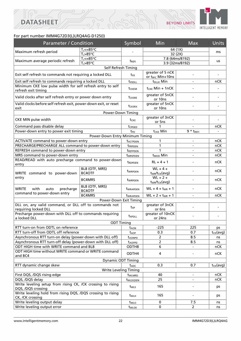
www.intelligentmemory.com 22 IMM4G72D3(L)LRQ4AG
For part number IMM4G72D3(L)LRQ4AG-D125(I)
Parameter / Condition Symbol Min Max Units
Maximum refresh period Tc<=85oC
- 64 (1X) ms
Tc>85oC 32 (2X)
Maximum average periodic refresh Tc<=85oC
tREFI 7.8 (64ms/8192)
us Tc>85oC 3.9 (32ms/8192)
Self Refresh Timing
Exit self refresh to commands not requiring a locked DLL tXS greater of 5 nCK
or tRFC Min+10ns - -
Exit self refresh to commands requiring a locked DLL tXSDLL tDLLK Min - nCK
Minimum CKE low pulse width for self refresh entry to self refresh exit timing
tCKESR tCKE Min + 1nCK - -
Valid clocks after self refresh entry or power down entry tCKSRE greater of 5nCK
or 10ns - -
Valid clocks before self refresh exit, power-down exit, or reset exit
tCKSRX greater of 5nCK
or 10ns - -
Power-Down Timing
CKE MIN pulse width tCKE greater of 3nCK
or 5ns - -
Command pass disable delay tCPDED 1 - nCK
Power-down entry to power exit timing tPD tCKE Min 9 * tREFI -
Power-Down Entry Minimum Timing
ACTIVATE command to power-down entry tACTPDEN 1 - nCK
PRECHARGE/PRECHARGE ALL command to power-down entry tPRPDEN 1 - nCK
REFRESH command to power-down entry tREFPDEN 1 - nCK
MRS command to power-down entry tMRSPDEN tMOD Min - nCK
READ/READ with auto precharge command to power-down entry
tRDPDEN RL + 4 + 1 - nCK
WRITE command to power-down entry
BL8 (OTF, MRS) BC4OTF
tWRPDEN WL + 4 +
tWR/tCK(avg) - nCK
BC4MRS tWRPDEN WL + 2 +
tWR/tCK(avg) - nCK
WRITE with auto precharge command to power-down entry
BL8 (OTF, MRS) BC4OTF
tWRAPDEN WL + 4 + tWR + 1 - nCK
BC4MRS tWRAPDEN WL + 2 + tWR + 1 - nCK
Power-Down Exit Timing
DLL on, any valid command, or DLL off to commands not requiring locked DLL
tXP greater of 3nCK
or 6ns - -
Precharge power-down with DLL off to commands requiring a locked DLL
tXPDLL greater of 10nCK
or 24ns - -
ODT Timing
RTT turn-on from ODTL on reference tAON -225 225 ps
RTT turn-off from ODTL off reference tAOF 0.3 0.7 tCK(avg)
Asynchronous RTT turn-on delay (power-down with DLL off) tAONPD 2 8.5 ns
Asynchronous RTT turn-off delay (power-down with DLL off) tAOFPD 2 8.5 ns
ODT HIGH time with WRITE command and BL8 ODTH8 6 - nCK
ODT HIGH time without WRITE command or WRITE command and BC4
ODTH4 4 - nCK
Dynamic ODT Timing
RTT dynamic change skew tADC 0.3 0.7 tCK(avg)
Write Leveling Timing
First DQS, /DQS rising edge tWLMRD 40 - nCK
DQS, /DQS delay tWLDQSEN 25 - nCK
Write leveling setup from rising CK, /CK crossing to rising DQS, /DQS crossing
tWLS 165 - ps
Write leveling hold from rising DQS, /DQS crossing to rising CK, /CK crossing
tWLH 165 - ps
Write leveling output delay tWLO 0 7.5 ns
Write leveling output error tWLOE 0 2 ns

www.intelligentmemory.com 23 IMM4G72D3(L)LRQ4AG
For part number IMM4G72D3(L)LRQ4AG-D125(I)
Table 19 - SPD Information
Byte NO. Description Note Hex
1.35V 1.5V 1.35V 1.5V
0 Number of Serial PD Bytes Written / SPD Device Size / CRC Coverage
176 / 256 / 0-116 92
1 SPD Revision 1.2 12 2 Key Byte / DRAM Device Type DDR3 SDRAM 0B 3 Key Byte / Module Type Load Reduced DIMM 0B 4 SDRAM Density and Banks 4Gb 8banks 04 5 SDRAM Addressing Row 16 / Col 11 22 6 Module Nominal Voltage, VDD 1.35V/1.5V 1.5V 02 00 7 Module Organization 4Rank , x4 18 8 Module Memory Bus Width ECC, 72bit 0B 9 Fine Timebase (FTB) Dividend and Divisor 2.5ps 52 10 Medium Timebase (MTB) Dividend 1/8 (0.125ns) 01 11 Medium Timebase (MTB) Divisor 1/8 (0.125ns) 08 12 SDRAM Minimum Cycle Time (tCK min) 1.25ns 0A 13 Reserved - 00 14 CAS Latencies Supported, Least Significant Byte 6, 7, 8, 9, 10, 11 FE 15 CAS Latencies Supported, Most Significant Byte - 00 16 Minimum CAS Latency Time (tAA min) 13.125ns 69 17 Minimum Write Recovery Time (tWR min) 15ns 78 18 Minimum /RAS to /CAS Delay Time (tRCD min) 13.125ns 69
19 Minimum Row Active to Row Active Delay Time (tRRD min)
7.5ns 3C
20 Minimum Row Precharge Time (tRP min) 13.125ns 69 21 Upper Nibbles for tRAS and tRC - 11 22 Minimum Active to Precharge Time (tRAS min), LSB 35ns 18 23 Minimum Active to Active/Refresh Time (tRC min), LSB 48.125ns 81 24 Minimum Refresh Recovery Time (tRFC min), LSB 260ns 20 25 Minimum Refresh Recovery Time (tRFC min), MSB 260ns 08
26 Minimum Internal Write to Read Command Delay Time (tWTR min)
7.5ns 3C
27 Minimum Internal Read to Precharge Command Delay Time (tRTP min)
7.5ns 3C
28 Upper Nibble for tFAW - 01
29 Minimum Four Activate Window Delay Time (tFAW min), LSB
30ns 40
30 SDRAM Optional Features DLL off Mode, RZQ/6,
RZQ/7 83
31 SDRAM Thermal and Refresh Options 0-95oC Op. Temp. w/2x
refresh 05
32 Module Thermal Sensor With TS 80 33 SDRAM Device Type Non-Standard SDRAM A1 34 Fine Offset for SDRAM Minimum Cycle Time (tCKmin) - 00
35-59 Reserved, General Section - 00 60 Module Nominal Height 30<height<=31 (mm) 10
61 Module Maximum Thickness 2< Tf <=3 (mm); 1< Tb <=2 (mm)
12
62 Reference Raw Card Used Raw Card C0 02
63 Module Attributes 2 Row of DRAM,
Odd ranks are mirrored 09

www.intelligentmemory.com 24 IMM4G72D3(L)LRQ4AG
Byte NO. Description Note Hex
64 memory Buffer Revision Number Undefined FF 65 Register vendor ID code (LSB) - 00 66 Register vendor ID code (MSB) - 00
67 F0RC3 / F0RC2 - Timing Control & Drive Strength, CA & CS
Moderate / Strong drive Not swapped / Standard
60
68 F0RC5 / F0RC4 - Drive Strength, ODT & CKE and Y Moderate drive 55
69 F1RC11 / F1RC8 - Extended Delay for Y, CS and ODT & CKE
No delay 00
70 F1RC13 / F1RC12 - Additive Delay for CS and CA Disabled 00 71 F1RC15 / F1RC14 - Additive Delay for ODT & CKE Disabled 00
72 F3RC9 / F3RC8 - MDQ Termination and Drive Strength for 800 & 1066
RZQ/6, RZQ/2 02
73 F[3,4]RC11 / F[3,4]RC10 - Rank 0 & 1 RD & WR QxODT Control for 800 & 1066
F4RC11(QxODT1), F3RC11(QxODT0)
90
74 F[5,6]RC11 / F[5,6]RC10 - Rank 2 & 3 RD & WR QxODT Control for 800 & 1066
Not asserted 00
75 F[7,8]RC11 / F[7,8]RC10 - Rank 4 & 5 RD & WR QxODT Control for 800 & 1066
Not asserted 00
76 F[9,10]RC11 / F[9,10]RC10 - Rank 6 & 7 RD & WR QxODT Control for 800 & 1066
Not asserted 00
77 MR1,2 Registers for 800 & 1066 RZQ/2, Rtt_Nom disabled, RZQ/7
81
78 F3RC9 / F3RC8 - MDQ Termination and Drive Strength for 1333 & 1600
RZQ/7, RZQ/4 11
79 F[3,4]RC11 / F[3,4]RC10 - Rank 0 & 1 RD & WR QxODT Control for 1333 & 1600
F[3,4]RC11 F0
80 F[5,6]RC11 / F[5,6]RC10 - Rank 2 & 3 RD & WR QxODT Control for 1333 & 1600
F5RC11(QxODT1), F6RC11(QxODT0)
60
81 F[7,8]RC11 / F[7,8]RC10 - Rank 4 & 5 RD & WR QxODT Control for 1333 & 1600
Not asserted 00
82 F[9,10]RC11 / F[9,10]RC10 - Rank 6 & 7 RD & WR QxODT Control for 1333 & 1600
Not asserted 00
83 MR1,2 Registers for 1333 & 1600 RZQ/2, RZQ/4, RZQ/7 85
84 F3RC9 / F3RC8 - MDQ Termination and Drive Strength for 1866 & 2133
RZQ/9, RZQ/4 31
85 F[3,4]RC11 / F[3,4]RC10 - Rank 0 & 1 RD & WR QxODT Control for 1866 & 2133
F[3,4]RC11 F0
86 F[5,6]RC11 / F[5,6]RC10 - Rank 2 & 3 RD & WR QxODT Control for 1866 & 2133
F6RC11(QxODT0), F5RC11(QxODT1)
60
87 F[7,8]RC11 / F[7,8]RC10 - Rank 4 & 5 RD & WR QxODT Control for 1866 & 2133
Not asserted 00
88 F[9,10]RC11 / F[9,10]RC10 - Rank 6 & 7 RD & WR QxODT Control for 1866 & 2133
Not asserted 00
89 MR1,2 Registers for 1866 & 2133 RZQ/2, RZQ/8, RZQ/7 95 90 Minimum Module Delay Time for 1.5 V 7.5 ns 3C 91 Maximum Module Delay Time for 1.5 V 9.5 ns 4C 92 Minimum Module Delay Time for 1.35 V 7.5 ns 3C 93 Maximum Module Delay Time for 1.35 V 9.5 ns 4C 94 Minimum Module Delay Time for 1.25 V 7.5 ns 3C 95 Maximum Module Delay Time for 1.25 V 9.5 ns 4C
96-101 Reserved - 00 102-116 Memory Buffer Personality Bytes Undefined 00 117-118 Module ID: Module Manufacturer’s JEDEC ID Code Reserved Reserved
119 Module ID: Module Manufacturing Location Reserved Reserved 120-121 Module ID: Module Manufacturing Date Reserved Reserved

www.intelligentmemory.com 25 IMM4G72D3(L)LRQ4AG
Byte NO. Description Note Hex
122-125 Module ID: Module Serial Number Reserved Reserved 126-127 Cyclical Redundancy Code - B5 8A 4F 4C 128-145 Module Part Number Reserved Reserved 146-147 Module Revision Code Reserved Reserved 148-149 DRAM Manufacturer’s JEDEC ID Code Reserved Reserved 150-175 Manufacturer’s Specific Data Reserved Reserved 176-255 Open For Customer Use Reserved Reserved

www.intelligentmemory.com 26 IMM4G72D3(L)LRQ4AG
Revision History
Revision Descriptions Release Date
1.0 Initial release May, 2021

www.intelligentmemory.com 27 IMM4G72D3(L)LRQ4AG
Contents
Features 2
Table 1 - Ordering Information for RoHS Compliant Product 3
Table 2 - Operating Voltage 3
Table 3 - Temperature Grade 3
Table 4 - Speed Grade 3
Table 5 - Memory Chip Information 3
Part Number Decoder 4
Table 6 - Addressing 4
Table 7 - Pin Assignment 5
Table 8 - Pin Description 6
Module Dimension 7
Figure 1 - 240 Pin DDR3 SDRAM Load Reduced DIMM 7
Table 9 - PCB Dimension 7
Figure 2 - Functional Block Diagram (Page 1 of 6) 8
Figure 3 - Functional Block Diagram (Page 2 of 6) 9
Figure 4 - Functional Block Diagram (Page 3 of 6) 10
Figure 5 - Functional Block Diagram (Page 4 of 6) 11
Figure 6 - Functional Block Diagram (Page 5 of 6) 12
Figure 7 - Functional Block Diagram (Page 6 of 6) 13
Table 10 - Absolute Maximum DC Ratings 14
Table 11 - DC Electrical Characteristics and Operating Conditions 14
Table 12 - DC Electrical Characteristics and Input Conditions 15
Table 13 - Input Switching Conditions 16
Table 14 - Differential Input Operating Conditions (CK, /CK and DQS, /DQS) 17
Table 15 - Single-Ended Output Driver Characteristics 17
Table 16 - Differential Output Driver Characteristics 18
Table 17 - IDD Specifications with Conditions and Operation Current 19
Table 18 - AC Timing Parameter and Operating Conditions 20
Table 19 - SPD Information 23
Revision History 26
Contents 27
List of Tables 28
List of Figures 28

www.intelligentmemory.com 28 IMM4G72D3(L)LRQ4AG
List of Tables
Table 1 - Ordering Information for RoHS Compliant Product 3
Table 2 - Operating Voltage 3
Table 3 - Temperature Grade 3
Table 4 - Speed Grade 3
Table 5 - Memory Chip Information 3
Table 6 - Addressing 4
Table 7 - Pin Assignment 5
Table 8 - Pin Description 6
Table 9 - PCB Dimension 7
Table 10 - Absolute Maximum DC Ratings 14
Table 11 - DC Electrical Characteristics and Operating Conditions 14
Table 12 - DC Electrical Characteristics and Input Conditions 15
Table 13 - Input Switching Conditions 16
Table 14 - Differential Input Operating Conditions (CK, /CK and DQS, /DQS) 17
Table 15 - Single-Ended Output Driver Characteristics 17
Table 16 - Differential Output Driver Characteristics 18
Table 17 - IDD Specifications with Conditions and Operation Current 19
Table 18 - AC Timing Parameter and Operating Conditions 20
Table 19 - SPD Information 23
List of Figures
Figure 1 - 240 Pin DDR3 SDRAM Load Reduced DIMM 7
Figure 2 - Functional Block Diagram (Page 1 of 6) 8
Figure 3 - Functional Block Diagram (Page 2 of 6) 9
Figure 4 - Functional Block Diagram (Page 3 of 6) 10
Figure 5 - Functional Block Diagram (Page 4 of 6) 11
Figure 6 - Functional Block Diagram (Page 5 of 6) 12
Figure 7 - Functional Block Diagram (Page 6 of 6) 13