imperial journal of interdisciplinary research (ijir) vol ... · multistandard wireless receivers,...
TRANSCRIPT

Imperial Journal of Interdisciplinary Research (IJIR) Vol-2, Issue-7, 2016 ISSN: 2454-1362, http://www.onlinejournal.in
Imperial Journal of Interdisciplinary Research (IJIR) Page 474
Design and Implementation of Efficient Carry Select Adder on Reconfigurable Device Using Novel Logic Formulation
Subha.K1, G.Nusrath Sumaiya2 & S.Murugavalli3
1,2,3Assistant Professor, M.A.M School of engineering, Tamil Nadu, India
Abstract; Carry Select Adder (CSLA) is one of the fastest adders used in many data-processing processors to perform fast arithmetic functions. The logic operations involved in conventional carry select adder (CSLA) and binary to excess-1 converter (BEC)-based CSLA are data dependence and redundant logic operations. In this paper, proposed a new logic formulation for CSLA to eliminate the redundant logic operations present in the conventional CSLA. In the proposed scheme, the carry select (CS) operation is scheduled before the calculation of final-sum, which is different from the conventional approach. The proposed CSLA design has reduced area and delay as compared with BEC-based CSLA. Due to the small carry-output delay, the proposed CSLA design is suitable for Multistage CSLA(SQRT-CSLA).The performance of the CSLA is evaluated by implementing a MAC unit using either conventional, BEC or proposed CSLA in the adder part, for different bit-widths. This work focuses on the performance of CSLA in terms of area, delay and power. The analysis of the result shows that the MAC unit using proposed SQRT-CSLA has less area, delay and power when compared with MAC unit with existing SQRT-CSLAs. The system has been designed efficiently using Verilog HDL codes and simulated using Quartus II 9.1.The hardware implementation is done by using Altera-FPGA.
Index Terms— Carry Select Adder (CSLA), BEC, Multistage CSLA(SQRT-CSLA)
1. Introduction
1.1 Adders
Design of area and power-efficient high-speed data path logic systems are one of the most areas of research in VLSI system design are increasingly used in portable and mobile devices, multistandard wireless receivers, and biomedical instrumentation. An adder is the main component of an arithmetic unit. In electronic applications adders are most widely used. A complex digital signal processing (DSP) system involves several
adders. An efficient adder design essentially improves the performance of a complex DSP system. Some other applications of adders are in Multiply – Accumulate (MAC) unit. Adders are also used in multipliers, in high speed integrated circuits and in digital signal processing to execute various algorithms like FFT, IIR and FIR. Therefore, regarding the efficient implementation of an arithmetic unit, the binary adder structures become a very critical hardware unit.
Large number of different circuit architectures with different performance characteristics and widely used in the practice. Although many researches dealing with the binary adder structures have been done, the studies based on their comparative performance analysis are only a few. In this project, qualitative evaluations of the classified binary adder architectures are given. Among the huge member of the adders we wrote VHDL (Hardware Description Language) code for Ripple-carry, Carry-select and Carry-look ahead to emphasize the common performance properties belong to their classes. In the following section, we give a brief description of the studied adder architectures.
Table 1.1: Categorization of adders with respect to delay time and capacity
1.1.1 Ripple Carry Adder (RCA)
Ripple carry adder is composed of cascaded full adders for n-bit adder, as shown in figure.1.1.It is constructed by cascading full adder

Imperial Journal of Interdisciplinary Research (IJIR) Vol-2, Issue-7, 2016 ISSN: 2454-1362, http://www.onlinejournal.in
Imperial Journal of Interdisciplinary Research (IJIR) Page 475
blocks in series. The carry out of one stage is fed directly to the carry-in of the next stage. For an n-bit parallel adder it requires n full adders.
Figure 1.1 4-Bit Ripple Carry Adder
Drawbacks
Not very efficient when large number bit numbers are used.
Delay increases linearly with bit length.
Delay
Delay from Carry-in to Carry-out is more important than from A to carry-out or carry-in to SUM, because the carry-propagation chain will determine the latency of the whole circuit for a Ripple-Carry adder. Considering the above worst-case signal propagation path we can thus write the following equation. For a k-bit RCA worst case path delay is
TRCA-k bit = TFA(x0, y0 c0) + (k-2)* TFA(Cin Ci) + TFA(Cin Sk-1) .
Logic Equations
gi = ai bi (1.1) p = ai xor bi (1.2) Si = pi xor ci (1.3) Ci+1 = gi + pi ci (1.4)
Complexity and Delay for N-Bit RCA Structure
ARCA = O (n) = 7n (1.5) TRCA = O (n) = 2n (1.6)
1.1.2 Carry Look Ahead Adders (CLA)
Carry Look Ahead Adder can produce carries faster due to carry bits generated in parallel by an additional circuitry whenever inputs change. This technique uses carry bypass logic to speed up the carry propagation.
Figure 1.2 4-Bit CLA Logic Equations
Let ai and bi be the augends and addend inputs, ci the carry input, Si and Ci+1, the sum and carry-out to the ith bit position. If the auxiliary functions, pi and gi called the propagate and generate signals, the sum output respectively are defined as follows.
pi = ai + bi. (1.7) gi = ai bi. (1.8) Si = ai xor bi xor ci. (1.9) Ci+1 = gi + pi ci. (2.0)
As increase the no of bits in the Carry Look Ahead adders, the complexity increases because the no. of gates in the expression Ci+1 increases. So practically its not desirable to use the traditional CLA shown above because it increase the Space required and the power too.
1.1.3 Carry Select Adders (CSLA)
In Carry select adder scheme, blocks of bits are added in two ways: one assuming a carry-in of 0 and the other with a carry-in of 1.This results in two precomputed sum and carry-out signal pairs (s0
i-1:k , c0i ; s1
i-1:k , c1i) , later as the block’s true
carry-in (ck) becomes known , the correct signal pairs are selected. Generally multiplexers are used to propagate carries.

Imperial Journal of Interdisciplinary Research (IJIR) Vol-2, Issue-7, 2016 ISSN: 2454-1362, http://www.onlinejournal.in
Imperial Journal of Interdisciplinary Research (IJIR) Page 476
Figure 1.3 A Carry Select Adder with 1 level using n/2- bit RCA
Because of multiplexers larger area is required.
Have a lesser delay than Ripple Carry Adders (half delay of RCA).
Hence we always go for Carry Select Adder while working with smaller no of bits.
Logic Equations
si-1:k = ck s0i-1:k + ck s1
i-1:k . (2.1)
ci = ck c0i + ck c1
i. (2.2) Complexity and Delay for N-Bit CSLA Structure
ACSLA = O (n) = 14n (2.3) TCSLA = O (n1/*l+1) = 2.8n1/2 (2.4)
1.1.4 Analysis of Adders
Comparison of 3- different adders Ripple Carry Adders, Carry Look Ahead Adders and the Carry Select Adders. The basic purpose of our experiment was to know the time and power trade-offs between different adders which will give us a clear picture of which adder suits best in which type of situation during design process. Hence below we present both the theoretical and practical comparisons of all the three adders whish were taken into consideration.
Table 1.2 Theoretical Comparison of Area Occupied (Ax)
Adder Name Complex(Ax) Area for n-bit
Ripple Carry Adder(RCA)
O(n) 7n
Carry Look Ahead Adder(CLA)
O(n) 4n
Carry Select Adder(CSLA)
O(n) 14n
Table 1.3 Comparison Of Time Required.
1.1.5 Comparison among Adders
As can be seen above stated the theoretical comparison of AREA required and both the theoretical and simulated value of TIME required. The values stated above are the values for 8-bit adders. So analyzing the above facts reached at the following conclusions about different adders and intelligent use of them in different circumstances according to the SPACE TIME trade-off. The results can be summarized as follows.
Regarding the circuit area complexity in the adder architectures, the ripple-carry adder (RCA) in the first class is the most efficient one, but the carry select adder (CSLA) in the fourth class with highest complexity is the least efficient one.
Considering the circuit delay time, Carry Select Adder (CSLA) is the fastest one for every n-bit length, so has the shortest delay. Otherwise, Ripple Carry Adder (RCA) is the slowest one, due to the long carry propagation.
Carry look ahead adder reduces the delay compared to ripple carry adder but as the adder size

Imperial Journal of Interdisciplinary Research (IJIR) Vol-2, Issue-7, 2016 ISSN: 2454-1362, http://www.onlinejournal.in
Imperial Journal of Interdisciplinary Research (IJIR) Page 477
increases complexity increases also, fan in to the gates increases. DeLay of the circuit depends upon, how many gates are connected in series and delay of a gate depends upon no of fan ins, so the later term dominates as adder size increases in carry look ahead adder.
Defined a term Area-Delay Product which gave the clear picture of the space-time trade-off. It is worthy to note that while consider all the adders discussed above Ripple Carry adders and Carry Select Adders are the two sides of the spectrum. Because, while Ripple Carry Adders have a smaller area and lesser speed, in contrast to which Carry Select adders have high speed (nearly twice the speed of Ripple Carry Adders) and occupy a larger area. Hence among the three, Carry Select Adder has the least Time.
1.2 Multiplier
Multiplication is a computation intensive and the core operation in many algorithms used in scientific computations. The computational complexity of algorithm used in digital signal processing (DSP) has gradually increased. As a result fast and efficient parallel multipliers are required for general purpose digital signal processors (DSPs) as well as application specific architectures for DSP.
Generally as we know multiplication goes in two basic steps, Partial product generation and partial addition. In multiplication the addition stage is in critical path that is it takes long delay and also it requires large hardware resources to compute product from partial product.
Figure 1.4-16bit Multiplier.
In particular, if the processing has to be performed under real time conditions, such algorithms have to deal with high throughput rates. In many cases implementation of DSP algorithm demands using application specific integrated circuits (ASICs). This is especially required for image processing applications. Since development
costs for ASICs are high, algorithms should be verified and optimized before implementation. However, with recent advancements in very large scale integration (VLSI) technology, hardware implementation has become a desirable alternative. Significant speedup in computation time can be achieved by assigning computation intensive tasks to hardware and by exploiting the parallelism in algorithms. Recently, field programmable gate arrays (FPGAs) have emerged as a platform of choice for efficient hardware implementation of computation intensive algorithms. FPGAs enable a high degree of parallelism and can achieve orders of magnitude speedup over general purpose processors (GPPs). This is a result of increasing embedded resources available on FPGA. FPGA have the benefit of hardware speed and the flexibility of software. The three main factors that play an important role in FPGA based design are the targeted FPGA architecture, electronic design automation (EDA) tools and design techniques employed at the algorithmic level using hardware description languages. In FPGAs, the choice of the optimum multiplier involves three key factors: area, propagation delay and reconfiguration time. Therefore, FPGA has become viable technology and an attractive alternative to ASICs. 1.3 Applications
DSP Multipliers Multimedia.
2.Proposed Method
2.1proposed Description
In the proposed scheme, the carry select (CS) operation is scheduled before the calculation of final-sum, which is different from the conventional approach. Bit patterns of two anticipating carry words (corresponding to cin = 0 and 1) and fixed cin bits are used for logic optimization of CS and generation units. An efficient CSLA design is obtained using optimized logic units. The proposed CSLA design involves significantly less area and delay than the recently proposed BEC-based CSLA. Due to the small carry-output delay, the proposed CSLA design is for Single stage CSLA. A theoretical estimate shows that the proposed CSLA involves nearly 26% less area–delay–product (ADP) than the BEC-based CSLA, which is best among the existing CSLA designs, for 64bit-widths.
Imperial Journal of Interdisciplinary Research (IJIR) Vol-2, Issue-7, 2016 ISSN: 2454-1362, http://www.onlinejournal.in
Imperial Journal of Interdisciplinary Research (IJIR) Page 478
2.2 Logic Formulation
The proposed logic formulation for the CSLA is given as
Co(i)=A(i).B(i) (2.1) C1
0 (i) = c10(i-1) . s0(i) + c0(i) for (c1
0(0) =0) (2.2)
= 1) (2.3) if ( (2.4)
if ( (2.5)
(2.6) (2.7)
The proposed CSLA is based on the logic formulation given in (2.1)–(2.7), and its structure is shown in Fig. 2.1.
Figure 2.1 Proposed carry select adder designs.
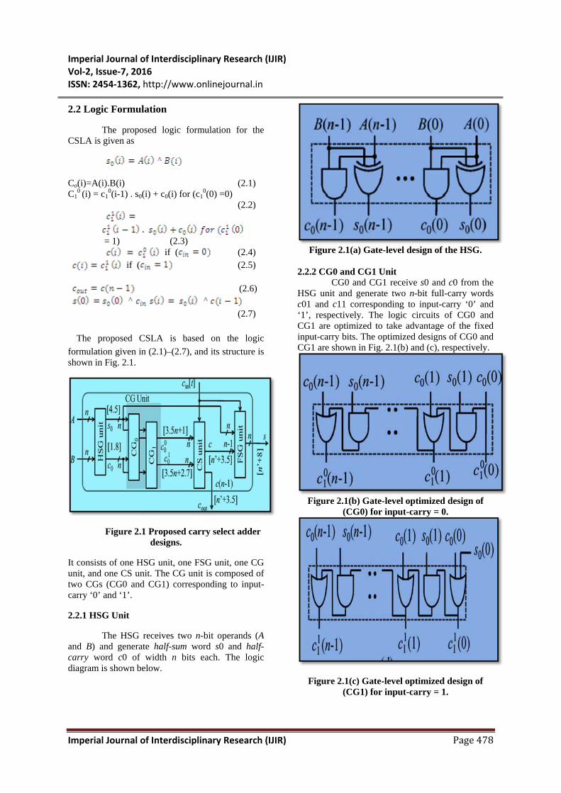
It consists of one HSG unit, one FSG unit, one CG unit, and one CS unit. The CG unit is composed of two CGs (CG0 and CG1) corresponding to input-carry ‘0’ and ‘1’.
2.2.1 HSG Unit
The HSG receives two n-bit operands (A and B) and generate half-sum word s0 and half-carry word c0 of width n bits each. The logic diagram is shown below.
Figure 2.1(a) Gate-level design of the HSG.
2.2.2 CG0 and CG1 Unit
CG0 and CG1 receive s0 and c0 from the HSG unit and generate two n-bit full-carry words c01 and c11 corresponding to input-carry ‘0’ and ‘1’, respectively. The logic circuits of CG0 and CG1 are optimized to take advantage of the fixed input-carry bits. The optimized designs of CG0 and CG1 are shown in Fig. 2.1(b) and (c), respectively.
Figure 2.1(b) Gate-level optimized design of
(CG0) for input-carry = 0.
Figure 2.1(c) Gate-level optimized design of (CG1) for input-carry = 1.

Imperial Journal of Interdisciplinary Research (IJIR) Vol-2, Issue-7, 2016 ISSN: 2454-1362, http://www.onlinejournal.in
Imperial Journal of Interdisciplinary Research (IJIR) Page 479
2.2.3 CS Unit
The CS unit selects one final carry word from the two carry words available at its input line using the control signal cin. It selects c01 when cin = 0; otherwise, it selects c11. The CS unit can be implemented using an n-bit 2-to-l MUX. However, we find from the truth table of the CS unit that carry words c01 and c11 follow a specific bit pattern. If c01(i) = ‘1’, then c11(i) = 1,irrespective of s0(i) and c0(i), for 0 ≤ i ≤ n − 1. This feature is used for logic optimization of the CS unit. The optimized design of the CS unit is shown in Fig. 2.1(d), which is composed of n AND–OR gates. The final carry word c is obtained from the CS unit.
Figure 2.1(d) Gate-level design of the CS unit. 2.2.4 FSG Unit
The MSB of c is sent to output as cout,
and (n − 1) LSBs are XORed with (n − 1) MSBs of half sum (s0) in the FSG [shown in Fig. 2.1(e)] to obtain (n − 1) MSBs of final-sum(s). The LSB of s0 is XORed with cin to obtain the LSB of s.
Figure 2.1(e) Gate-level design of the final-sum generation (FSG) unit.
2.3 MAC Unit Operation
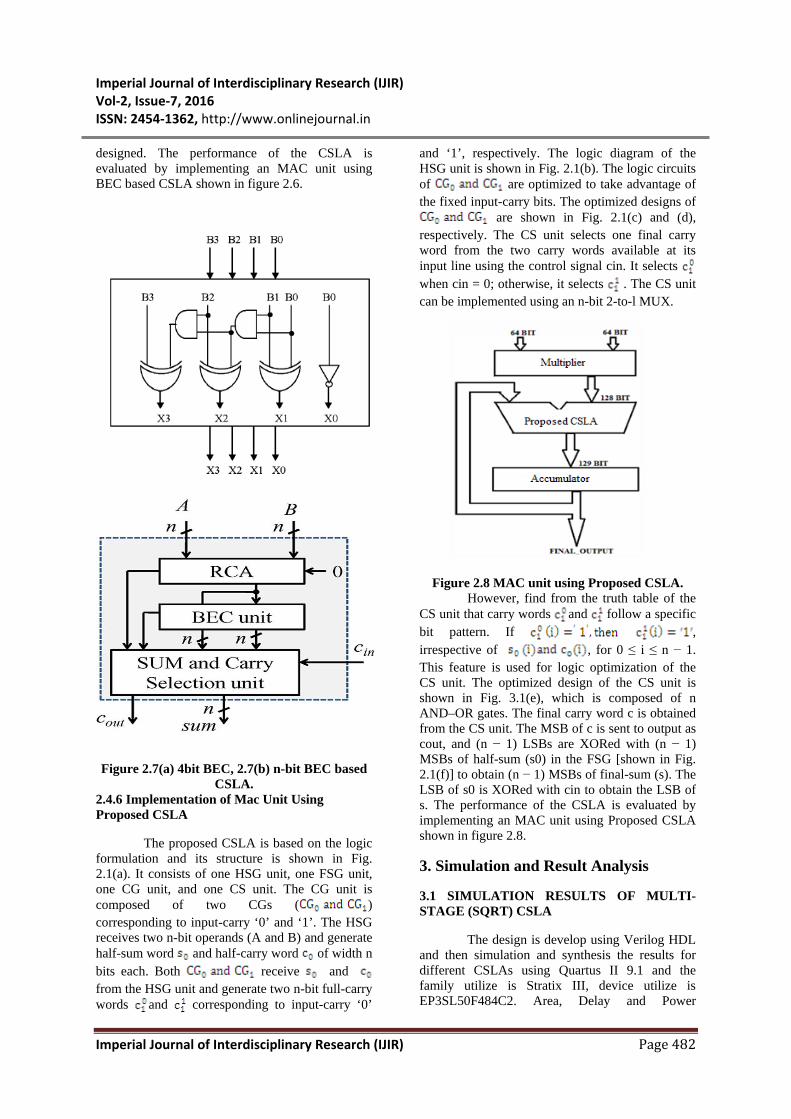
The Multiplier-Accumulator (MAC) operation is the key operation not only in DSP applications but also in multimedia information processing and various other applications. As mentioned above, MAC unit consist of multiplier, adder and register/accumulator. In this project, used 64 bit multiplier. The MAC inputs are obtained from the memory location and given to the multiplier block. This will be useful in 64 bit digital signal processor. The input which is being fed from the memory location is 64 bit. When the input is given to the multiplier it starts computing value for the given 64 bit input and hence the output will be 128 bits. The multiplier output is given as the input to three different adders which performs addition. The function of the MAC unit is given by following equation
F= Σ Pj Qj (2.8)
The output of three adders is 129 bit i.e. one bit is for the carry (128bits+ 1 bit). Then, the output is given to the accumulator register. The accumulator register used in this design is Parallel in Parallel out (PIPO). Since the bits are huge and also three CSLA adders produces all the output values in parallel, PIPO register is used where the input bits are taken in parallel and output is taken in parallel. The output of the accumulator register is taken out or fed back as one of the input to different three CSLA adders. The figure shows the basic architecture of MAC unit.
Figure 2.2 MAC unit Architecture.

Imperial Journal of Interdisciplinary Research (IJIR) Vol-2, Issue-7, 2016 ISSN: 2454-1362, http://www.onlinejournal.in
Imperial Journal of Interdisciplinary Research (IJIR) Page 480
2.4 Performance Comparison
2.4.1. Area–Delay Estimation Method
Consider all the gates to be made of 2-input AND, 2-input OR, and inverter (AOI). A 2-input XOR is composed of 2 AND, 1 OR, and 2
Table 2.1 Area and delay Of AND, OR, and NOT gates given in the saed 90-nm standard cell
library datasheet
NOT gates. The area and delay of the 2-input AND, 2-input OR, and NOT gates (shown in Table 3.1) are taken from the Synopsys Armenia Educational Department (SAED) 90-nm standard cell library datasheet for theoretical estimation. The delays of a design are calculated using the following relations:
A =a ・Na + r ・No + i ・Ni (2.9)
T =na ・Ta + no ・To + ni ・Ti (2.10)
Where (Na, No, Ni) and (na, no, ni), respectively, represent the (AND, OR, NOT) gate counts of the total design and its critical path. (a, r, i) and (Ta, To, Ti), respectively, represent the area and delay of one (AND, OR, NOT) gate. We have calculated the (AOI) gate counts of each design for area and delay estimation. Using (5a) and (5b), the area and delay of each design are calculated from the AOI gate counts (Na, No, Ni), (na, no, ni), and the cell details of Table 2.1.
2.4.2 Single-Stage CSLA
The general expression to calculate the AOI gate counts of the n-bit proposed BEC-based CSLA and conventional CSLA and are given in Table 2.1 of single stage design. Calculated the AOI gate counts on the critical path of the proposed n-bit CSLAand CSLAs and used those AOI gate counts in (3.9) to find an expression for delay of final-sum and output-carry in the unit of Ti (NOT gate delay). The delay of the n-bit single- stage CSLA for comparison. For further analysis of the critical path of the proposed CSLA, the delay of each intermediate and output signals of the proposed n-bit CSLA design of Fig.2.1 is shown.
Using the expressions of AOI gate details of Table 2.1, we have estimated the area and delay complexities of the proposed CSLA and the existing CSLA including the conventional one for input bit-widths. For the single-stage CSLA, the input-carry delay is assumed to be t = 0 and the delay of final-sum (fs) represents the adder delay.
The proposed CSLA involves nearly 27% less area and 1.3% less output power than that of conventional CSLA. Consequently, the conventional CSLA of involves 24% higher ADP and 13% higher PDP than the proposed CSLA, for 64bit-width. Compared with the BEC-based CSLA, the proposed CSLA design has marginally less ADP. However, in the BEC-based CSLA, delay increases at a much higher rate than the proposed CSLA design for higher bit widths. Compared with the BEC based CSLA, the proposed CSLA involves 1.6% more delay, but it involves nearly 26% less ADP and nearly 3% less PDP due to less area complexity. Power consumption is more in proposed single- stage CSLA when it compared with the existing CSLAs, to reduce the power consumption go for multi-stage CSLA.
2.4.3 Multistage CSLA (SQRT-CSLA)
The multipath carry propagation feature of the CSLA is fully exploited in the SQRT-CSLA, which is composed of a chain of CSLAs. CSLAs of increasing size are used in the SQRT-CSLA to extract the maximum concurrence in the carry propagation path. Using the SQRT-CSLA design, large-size adders are implemented with significantly less delay than a single-stage CSLA of same size. However, carry propagation delay between the CSLA stages of SQRT-CSLA is critical for the overall adder delay. Due to early generation of output-carry with multipath carry propagation feature, the proposed CSLA design is more suitable than the existing CSLA designs for area–delay efficient implementation of SQRT-CSLA. A 16-bit SQRT-CSLA design using the proposed CSLA is shown in Fig. 2.3, where the 2-bit RCA, 2-bit CSLA, 3-bit CSLA, 4-bit CSLA, and 5-bit CSLA are used. Considered the cascaded configuration for different bit-widths. To demonstrate the advantage of the proposed CSLA design in SQRT-CSLA, estimated the area and delay of SQRT-CSLA using the proposed CSLA design and the BEC-based CSLA for bit-widths 16, 32, 64, 128.

Imperial Journal of Interdisciplinary Research (IJIR) Vol-2, Issue-7, 2016 ISSN: 2454-1362, http://www.onlinejournal.in
Imperial Journal of Interdisciplinary Research (IJIR) Page 481
Figure 2.3 Proposed SQRT-CSLA for n = 16
2.4.4 Implementation of Mac Unit Using Conventional CSLA
A carry-select adder is a particular way to implement an adder, which is a logic element that computes the (n+1) bit sum of two -bit numbers. The carry-select adder is simple but rather fast, having a gate level depth of O√n.
Figure 2.4 MAC unit using Conventional CSLA.
The carry-select adder generally consists of two ripple carry adders and a multiplexer, shown in figure 2.5. Adding two n-bit numbers with a carry-select adder is done with two adders (therefore two ripple carry adders) in order to perform the calculation twice, one time with the assumption of the carry being zero and the other assuming one. After the two results are calculated, the correct sum, as well as the correct carry, is then selected with the multiplexer once the correct carry is known.
Figure 2.5 4 bit Conventional CSLA.
2.4.5 Implementation of Mac Unit Using BEC based CSLA
The conventional CSLA is not area efficient and delay for the operation is more because it uses multiple set of Ripple Carry Adders (RCA) to generate partial sum and carry by considering carry input and then the final sum and carry are selected by the multiplexers.
Figure 2.6 MAC unit using BEC based
CSLA. To avoid this problem, the regular CSLA
structure is modified using n-bit Binary to Excess-1 code converter (BEC) to improve the speed of operation. To improve the speed of operation use the Binary to Excess-1 Converter (BEC) instead of RCA with Cin=1 in the regular CSLA to achieve less delay. A structure and the function table of a 4-b BEC function of the CSLA is obtained by using the 4-bit BEC together with the mux. One input of the 8:4 mux gets as it input (B3, B2, B1, and B0) and another input of the mux is the BEC output. This produces the two possible partial results in parallel and the mux is used to select either the BEC output or the direct inputs according to the control signal Cin. The importance of the BEC logic stems from the large silicon area reduction when the CSLA with large number of bits are
Imperial Journal of Interdisciplinary Research (IJIR) Vol-2, Issue-7, 2016 ISSN: 2454-1362, http://www.onlinejournal.in
Imperial Journal of Interdisciplinary Research (IJIR) Page 482
designed. The performance of the CSLA is evaluated by implementing an MAC unit using BEC based CSLA shown in figure 2.6.
Figure 2.7(a) 4bit BEC, 2.7(b) n-bit BEC based CSLA.
2.4.6 Implementation of Mac Unit Using Proposed CSLA
The proposed CSLA is based on the logic formulation and its structure is shown in Fig. 2.1(a). It consists of one HSG unit, one FSG unit, one CG unit, and one CS unit. The CG unit is composed of two CGs ( ) corresponding to input-carry ‘0’ and ‘1’. The HSG receives two n-bit operands (A and B) and generate half-sum word and half-carry word of width n bits each. Both receive and from the HSG unit and generate two n-bit full-carry words and corresponding to input-carry ‘0’
and ‘1’, respectively. The logic diagram of the HSG unit is shown in Fig. 2.1(b). The logic circuits of are optimized to take advantage of the fixed input-carry bits. The optimized designs of
are shown in Fig. 2.1(c) and (d), respectively. The CS unit selects one final carry word from the two carry words available at its input line using the control signal cin. It selects when cin = 0; otherwise, it selects . The CS unit can be implemented using an n-bit 2-to-l MUX.
Figure 2.8 MAC unit using Proposed CSLA. However, find from the truth table of the
CS unit that carry words and follow a specific bit pattern. If , irrespective of , for 0 ≤ i ≤ n − 1. This feature is used for logic optimization of the CS unit. The optimized design of the CS unit is shown in Fig. 3.1(e), which is composed of n AND–OR gates. The final carry word c is obtained from the CS unit. The MSB of c is sent to output as cout, and (n − 1) LSBs are XORed with (n − 1) MSBs of half-sum (s0) in the FSG [shown in Fig. 2.1(f)] to obtain (n − 1) MSBs of final-sum (s). The LSB of s0 is XORed with cin to obtain the LSB of s. The performance of the CSLA is evaluated by implementing an MAC unit using Proposed CSLA shown in figure 2.8.
3. Simulation and Result Analysis
3.1 SIMULATION RESULTS OF MULTI-STAGE (SQRT) CSLA
The design is develop using Verilog HDL and then simulation and synthesis the results for different CSLAs using Quartus II 9.1 and the family utilize is Stratix III, device utilize is EP3SL50F484C2. Area, Delay and Power

Imperial Journal of Interdisciplinary Research (IJIR) Vol-2, Issue-7, 2016 ISSN: 2454-1362, http://www.onlinejournal.in
Imperial Journal of Interdisciplinary Research (IJIR) Page 483
Calculations have found for Different Multi stage CSLAs using Quartus II 9.1.
Figure 3.1 Simulation output of 16-bit
Conventional SQRT-CSLA.
Figure 3.2 Simulation output of 16-bit BEC
based SQRT- CSLA.
Figure 4.3 Simulation output of 16-bit Proposed
SQRT-CSLA.
3.2 Result Analysis of Multi-Stage (SQRT) CSLA
After the observation of simulation waveforms, synthesis is performed for calculation of delay and area and thereby the speed and power of the CSLA’s are calculated and a comparison of conventional, BEC and proposed CSLA is made in terms of delay, area and power and listed in the below table.
Table 3.1 Comparison of area, delay and power of existing and proposed for Multi -Stage CSLA.
POWER(mW)
128-bit
1.15
0.80
0.58
64-bit
1.32
1.35
0.51
32-bit
1.05
0.52
0.55
16-bit
1.76
1.29
0.50
DELAY(ns)
128-bit
57.051
22.403
21.826
64-bit
38.052
21.323
20.829
32-bit
21.434
16.458
16.512
16-bit
16.872
14.171
11.205

Imperial Journal of Interdisciplinary Research (IJIR) Vol-2, Issue-7, 2016 ISSN: 2454-1362, http://www.onlinejournal.in
Imperial Journal of Interdisciplinary Research (IJIR) Page 484
AREA (ALUTs)
128-bit
395
372
285
64-bit
188
189
173
32-bit
87
88
75
16-bit
41
37
41
DESIGN Conv CSLA BEC CSLA Pro CSLA
Table 4.2 Comparison of MAC unit implementation with Conventional, BEC and Proposed CSLA.
POWER(mW)
64-bit
20.46
18.13
19.92
32-bit
14.55
12.24
15.40
16-bit
10.61
15.52
10.01
DELAY(ns)
64-bit
20.800
9.826
8.026
32-bit
11.862
7.189
6.796
16-bit
8.039
5.737
5.258
AREA(ALUTs)
64-bit
488
431
376
32-bit
196
184
180
16-bit
84
76
80
DESIGN Conv CSLA BEC CSLA Pro CSLA
4. Conclusion
In this paper, analyzed the logic operations involved in the conventional and BEC-based CSLAs are data dependence and redundant logic operations. In this paper,sproposed a new logic formulation for CSLA to eliminate the redundant logic operations present in the conventional CSLA. In the proposed scheme, the CS operation is scheduled before the calculation of final-sum, which is different from the conventional approach. The proposed CSLA design involves significantly less area and delay than the recently proposed BEC-based CSLA. Due to the small carry output delay, the proposed CSLA design is suitable for the SQRT adder. All the three models of SQRT- CSLA are designed and are implemented in Verilog HDL using Quartus II 9.1 tool and the results are compared in terms of area, delay and power. The Proposed CSLA proves to be the High Speed and Low Power CSLA. The performance of this CSLA in terms of area, delay and power is evaluated by implementing an MAC unit by using the CSLA in
the adder part and again it proves to be the High Speed and Low Power CSLA. It is also implemented with Altera FPGA.The Proposed CSLA architecture is therefore, high speed, low power and area efficient for VLSI hardware implementation.
5.References [1]He .Y, Chang C. H., and Gu .Y. (2005) “An area-efficient 64-bit square root carry select adder for low power application,” in Proc. IEEE Int. Symp. Circuits Syst., vol. 4, pp. 4082–4085.
[2]Kim Y and Kim L.-S. (2001) “64-bit carry-select adder with reduced area,” Electron. Lett, vol. 37, no. 10, pp. 614–615.
[3]Manju S and Sornagopal (2013) “An efficient SQRT architecture of carry select adder design by common Boolean logic,” in Proc. VLSI ICEVENT pp. 1–5.
[4]Natalia A, Bystritskaya, Ilia A. Smolyannikov, Sergey I. Kurganskii (2010) “Investigation of properties of 36-bit Adders for creation of DSP Blocks on FPGA” International conference

Imperial Journal of Interdisciplinary Research (IJIR) Vol-2, Issue-7, 2016 ISSN: 2454-1362, http://www.onlinejournal.in
Imperial Journal of Interdisciplinary Research (IJIR) Page 485
[5]Padma Devi, Ashima Girdher, Balwinder (2010) “Singh Improved Carry Select Adder with Reduced Area and Low Power Consumption” International Journal of Computer Applications (0975 – 8887).
[6]Padmasri J.R, Christina P. A, Kavitha P and Mulla T (2013) “Modified area efficient carry select adder (MA-CSLA),” International Journal of Advanced Electrical and Electronics Engineering (IJAEEE) Volume-2, Issue-2.
[7]Prashanti P, Rajendra Naik B (2013) “Design and Implementation of High Speed Carry Select Adder,” in Proc. International Journal of Engineering Trends and Technology (IJETT) Volume 4 Issue 9.
[8] Ramkumar .B and Kittur. H.M, (2012) “Low-power and area-efficient carry-select adder,” IEEE Trans. Very Large Scale Integer. (VLSI) Syst., vol. 20, no. 2, pp. 371–375.
[9]Ravi J, Rama Rao K, Tirumala N (2014) “Design of Efficient FIR Filter MAC unit Using Parallel Prefix Adder,” in Proc. International Journal of Advanced Research in Computer and Communication Engineering Vol. 3, Issue 9. [10]Saranya k (2013) “Low Power and Area Efficient Carry Select Adder,” in Proc. International Journal of Soft Computing and Engineering (IJSCE).
[11]Wey I.-C., C.-C. Ho, Y.-S. Lin, and C. C. Peng, (2012) “An area-efficient carry select adder design by sharing the common Boolean logic term,” in Proc. IMECS, pp. 1–4.