implementation of 9x9 multiplications, wide-multiplier
TRANSCRIPT

Application Note AC398
Implementation of 9x9 Multiplications, Wide-Multiplier, and Extended Addition Using IGLOO2/SmartFusion2 Mathblock
Table of Contents
PurposeThis application note highlights the design guidelines and different implementation methods to achievebetter performance results while implementing wide-multipliers, 9-bit×9-bit multiplications, and extendedaddition with the IGLOO2/SmartFusion2 mathblock (MACC). The 9-bit×9-bit multiplications, wide-multiplier, and extended addition are ideal for applications with high-performance andcomputationally intensive signal processing operations. Some of them are finite impulse response (FIR)filtering, fast fourier transforms (FFTs), and digital up/down conversion. These functions are widely usedin video processing, 2D/3D image processing, wireless, industrial applications, and other digital signalprocessing (DSP) applications.
IntroductionThe IGLOO2/SmartFusion2 mathblock architecture has been optimized to implement various commonDSP functions with maximum performance and minimum logic resource utilization. The dedicated routingregion around the mathblock and the feedback paths provided in each mathblock result in routingimprovements. The IGLOO2/SmartFusion2 mathblock has a variety of features for fast and easyimplementation of many basic math functions. The high speed multiplier (9×9, 18×18), adder/subtractor,and accumulator in mathblock delivers high speed math functions. For more information onIGLOO2/SmartFusion2 mathblock, refer to IGLOO2 FPGA Fabric User's Guide/SmartFusion2 FPGAFabric User's Guide and for usage refer to the Inferring Microsemi SmartFusion2 MACC Blocksdocument.
This application note explains the design considerations and different methods for implementing thefollowing:
• Using 9x9 Multiplier Mode
• Wide-Multiplier
• Extended Addition
Purpose . . . . . . . . . . . . . . . . . . . . . . . . . . . . . . . . . . . . . . . . . . . . . . . . . . 1Introduction . . . . . . . . . . . . . . . . . . . . . . . . . . . . . . . . . . . . . . . . . . . . . . . . 1
Using 9x9 Multiplier Mode . . . . . . . . . . . . . . . . . . . . . . . . . . . . . . . . . . . . . . . . 2
Wide-Multiplier . . . . . . . . . . . . . . . . . . . . . . . . . . . . . . . . . . . . . . . . . . . . . . 12
Extended Addition . . . . . . . . . . . . . . . . . . . . . . . . . . . . . . . . . . . . . . . . . . . . 18
Conclusion . . . . . . . . . . . . . . . . . . . . . . . . . . . . . . . . . . . . . . . . . . . . . . . 24Appendix A - Design Files . . . . . . . . . . . . . . . . . . . . . . . . . . . . . . . . . . . . . . . . 24
Supers
eded
Supers
eded
June 2013 1
© 2013 Microsemi Corporation
Implementation of 9x9 Multiplications, Wide-Multiplier, and Extended Addition Using IGLOO2/SmartFusion2 Mathblock
Using 9x9 Multiplier Mode
OverviewThe 9-bit×9-bit multipliers are extensively used in low precision video processing applications. In videoapplications, the color conversion formats such as YUV to RGB, RGB to YUV, and RGB to YCbCr,NTSC, PAL etc., 9-bit×9-bit multipliers are used. In image processing, the operations involving 8-bit RGBsuch as 3×3, 5×5, 7×7 matrix multiplications, image enhancement techniques, scaling, resizing etc., 9-bit×9-bit multipliers are used. The IGLOO2/SmartFusion2 device addresses these applications byusing mathblock in DOTP mode.
The following sections explain the DOTP configurations and capabilities, guidelines, differentimplementation methods with design examples, and their performance and simulation results.
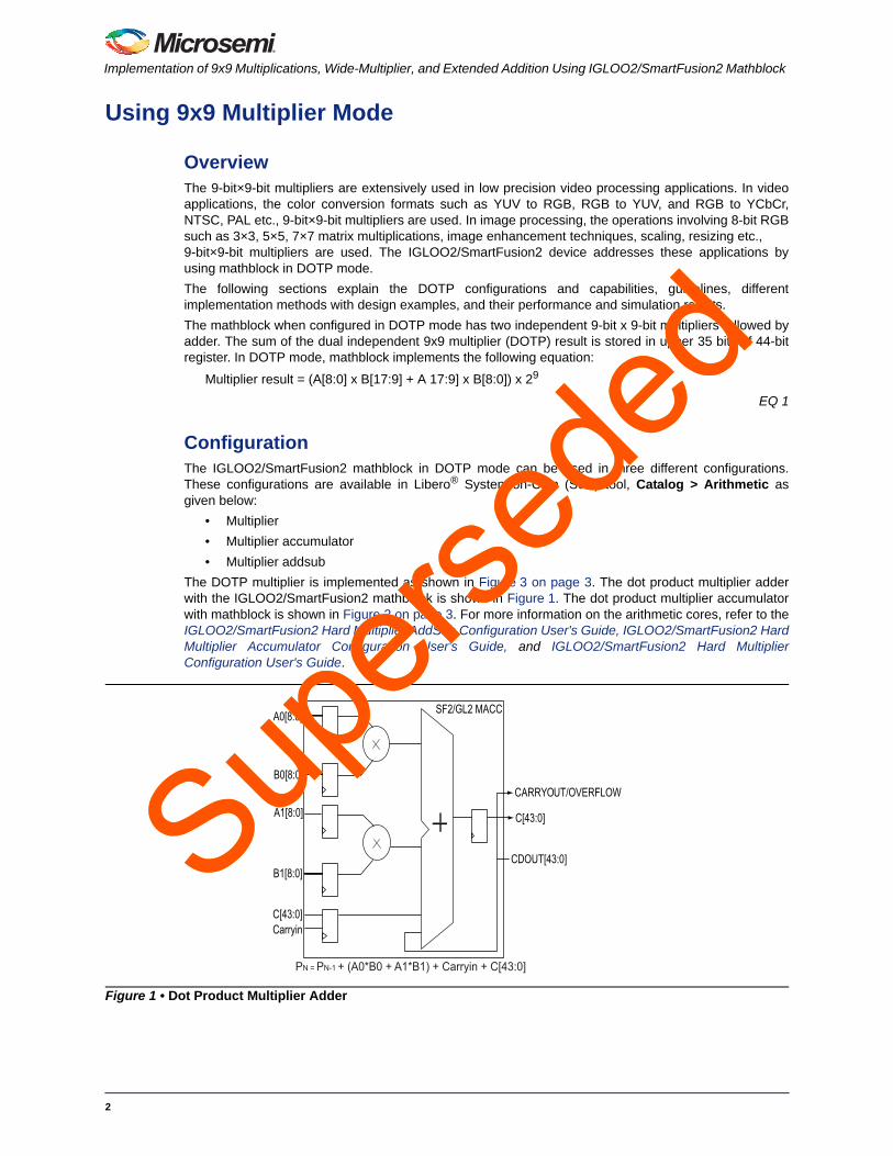
The mathblock when configured in DOTP mode has two independent 9-bit x 9-bit multipliers followed byadder. The sum of the dual independent 9x9 multiplier (DOTP) result is stored in upper 35 bits of 44-bitregister. In DOTP mode, mathblock implements the following equation:
Multiplier result = (A[8:0] x B[17:9] + A 17:9] x B[8:0]) x 29
EQ 1
ConfigurationThe IGLOO2/SmartFusion2 mathblock in DOTP mode can be used in three different configurations.These configurations are available in Libero® System-on-Chip (SoC) tool, Catalog > Arithmetic asgiven below:
• Multiplier
• Multiplier accumulator
• Multiplier addsub
The DOTP multiplier is implemented as shown in Figure 3 on page 3. The dot product multiplier adderwith the IGLOO2/SmartFusion2 mathblock is shown in Figure 1. The dot product multiplier accumulatorwith mathblock is shown in Figure 2 on page 3. For more information on the arithmetic cores, refer to theIGLOO2/SmartFusion2 Hard Multiplier AddSub Configuration User's Guide, IGLOO2/SmartFusion2 HardMultiplier Accumulator Configuration User's Guide, and IGLOO2/SmartFusion2 Hard MultiplierConfiguration User's Guide.
Figure 1 • Dot Product Multiplier Adder
A0[8:0] SF2/GL2 MACC
CARRYOUT/OVERFLOWB0[8:0]
A1[8:0]
B1[8:0]
C[43:0]Carryin
C[43:0]
CDOUT[43:0]
PN = PN-1 + (A0*B0 + A1*B1) + Carryin + C[43:0]
Supers
eded
Supers
eded
2

Using 9x9 Multiplier Mode
Figure 2 • Dot Product Multiplier Accumulator
PN = (A0*B0 + A1*B1) + Carryin + C[43:0] + CDIN
Carryin
B0[8:0]
SF2/GL2 MACC
P[43:0]
CARRYOUT/OVERFLOW
CDOUT[43:0]
0 or 1
0’s
CDIN
A0[8:0]
A1[8:0]
B1[8:0]
C[43:0]
Figure 3 • Dot Product Multiplier
A0[8:0]
P[18:0]
P = A0*B0 + A1*B1
SF2/GL2 MACC
B0[8:0]
A1[8:0]
B1[8:0]
Supers
eded
Supers
eded
3
Implementation of 9x9 Multiplications, Wide-Multiplier, and Extended Addition Using IGLOO2/SmartFusion2 Mathblock
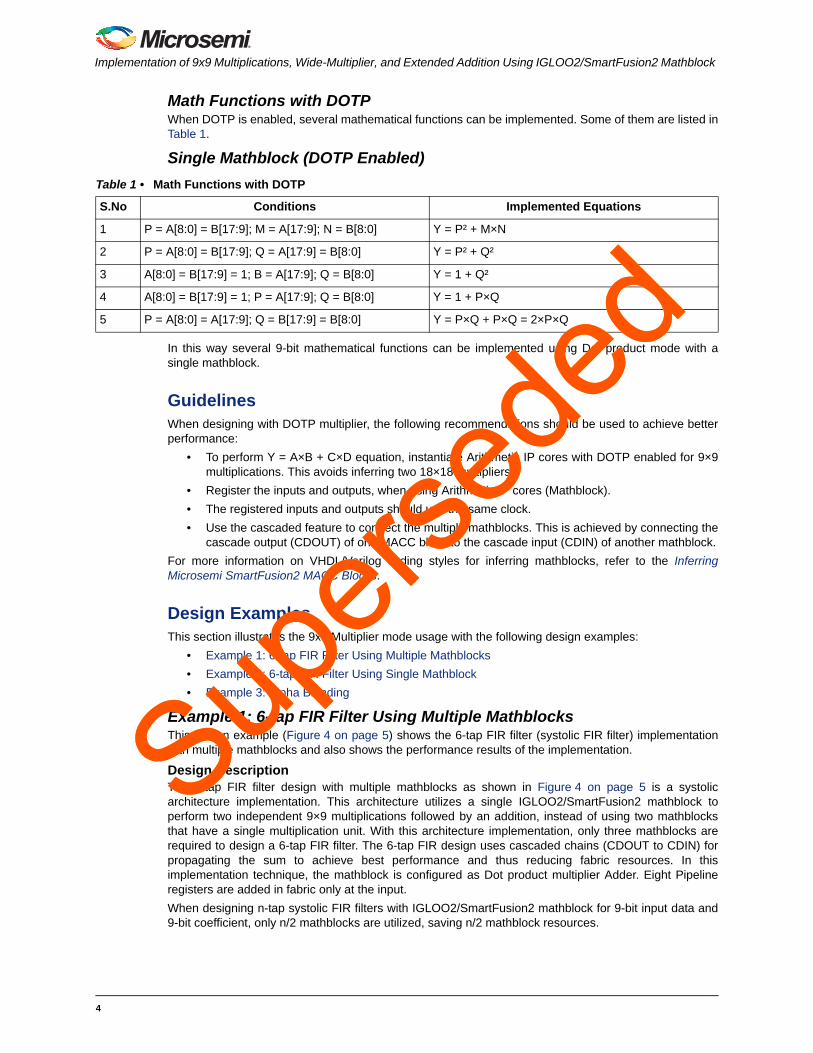
Math Functions with DOTPWhen DOTP is enabled, several mathematical functions can be implemented. Some of them are listed inTable 1.
Single Mathblock (DOTP Enabled)
In this way several 9-bit mathematical functions can be implemented using Dot product mode with asingle mathblock.
GuidelinesWhen designing with DOTP multiplier, the following recommendations should be used to achieve betterperformance:
• To perform Y = A×B + C×D equation, instantiate Arithmetic IP cores with DOTP enabled for 9×9multiplications. This avoids inferring two 18×18 multipliers.
• Register the inputs and outputs, when using Arithmetic IP cores (Mathblock).
• The registered inputs and outputs should use the same clock.
• Use the cascaded feature to connect the multiple mathblocks. This is achieved by connecting thecascade output (CDOUT) of one MACC block to the cascade input (CDIN) of another mathblock.
For more information on VHDL/Verilog coding styles for inferring mathblocks, refer to the InferringMicrosemi SmartFusion2 MACC Blocks.
Design Examples This section illustrates the 9x9 Multiplier mode usage with the following design examples:
• Example 1: 6-tap FIR Filter Using Multiple Mathblocks
• Example 2: 6-tap FIR Filter Using Single Mathblock
• Example 3: Alpha Blending
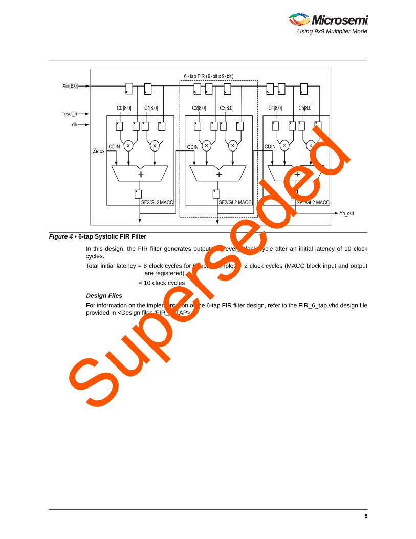
Example 1: 6-tap FIR Filter Using Multiple MathblocksThis design example (Figure 4 on page 5) shows the 6-tap FIR filter (systolic FIR filter) implementationwith multiple mathblocks and also shows the performance results of the implementation.
Design DescriptionThe 6-tap FIR filter design with multiple mathblocks as shown in Figure 4 on page 5 is a systolicarchitecture implementation. This architecture utilizes a single IGLOO2/SmartFusion2 mathblock toperform two independent 9×9 multiplications followed by an addition, instead of using two mathblocksthat have a single multiplication unit. With this architecture implementation, only three mathblocks arerequired to design a 6-tap FIR filter. The 6-tap FIR design uses cascaded chains (CDOUT to CDIN) forpropagating the sum to achieve best performance and thus reducing fabric resources. In thisimplementation technique, the mathblock is configured as Dot product multiplier Adder. Eight Pipelineregisters are added in fabric only at the input.
When designing n-tap systolic FIR filters with IGLOO2/SmartFusion2 mathblock for 9-bit input data and9-bit coefficient, only n/2 mathblocks are utilized, saving n/2 mathblock resources.
Table 1 • Math Functions with DOTP
S.No Conditions Implemented Equations
1 P = A[8:0] = B[17:9]; M = A[17:9]; N = B[8:0] Y = P² + M×N
2 P = A[8:0] = B[17:9]; Q = A[17:9] = B[8:0] Y = P² + Q²
3 A[8:0] = B[17:9] = 1; B = A[17:9]; Q = B[8:0] Y = 1 + Q²
4 A[8:0] = B[17:9] = 1; P = A[17:9]; Q = B[8:0] Y = 1 + P×Q
5 P = A[8:0] = A[17:9]; Q = B[17:9] = B[8:0] Y = P×Q + P×Q = 2×P×Q
Supers
eded
Supers
eded
4
Using 9x9 Multiplier Mode
In this design, the FIR filter generates outputs for every clock cycle after an initial latency of 10 clockcycles.
Total initial latency = 8 clock cycles for 6 input samples + 2 clock cycles (MACC block input and outputare registered).
= 10 clock cycles
Design Files
For information on the implementation of the 6-tap FIR filter design, refer to the FIR_6_tap.vhd design fileprovided in <Design files 'FIR_6_TAP>.
Figure 4 • 6-tap Systolic FIR Filter
reset_n
Xin[8:0]
clk
C0 [8:0] C1 [8:0] C2 [8:0] C5 [8:0]
CDIN CDIN CDIN
SF2/GL2 MACC SF2/GL2 MACC SF2/GL2 MACC
Yn_out
Zeros
C4 [8:0]C3 [8:0]
6 - tap FIR (9-bit x 9-bit)
Supers
eded
Supers
eded
5

Implementation of 9x9 Multiplications, Wide-Multiplier, and Extended Addition Using IGLOO2/SmartFusion2 Mathblock
Hardware ConfigurationFor 6-tap systolic FIR filter, mathblock is configured as Dot product multiplier adder with inputs andoutputs registered as shown in Figure 5.
Synthesis and Place-and-Route ResultsFigure 6 on page 7 shows the 6-tap systolic FIR filter resource utilization that uses multiple mathblocks.
Note: The results shown are specific for IGLOO2 device. Similar results can be achieved usingSmartFusion2 device. Refer to SmartFusion2 design files for more information.
Figure 5 • Dot Product Multiplier Adder for 6-tap Systolic FIRSupers
eded
Supers
eded
6

Using 9x9 Multiplier Mode
Resource Utilization
Place-and-Route Results
The frequency of operation achieved with this implementation after place-and-route is shown in Figure 7.
Simulation ResultsFigure 8 shows the post synthesis simulation results. The coefficient values (c0-c5) are configured indesign as C0 = 5, C1 = 3, C2 = 7, C3 = -4, C4 = 1, C5 = -2. The simulation results show that the 6-tap FIRfilter outputs on every clock cycle. It has an initial latency of 10 clock cycles.
Figure 6 • Resource Utilization for a 6-tap Systolic FIR Filter
Figure 7 • Place-and-Route Results for 6-tap Systolic FIR Filter
Figure 8 • 6-tap FIR Filter Post Synthesis Simulation
Supers
eded
Supers
eded
7

Implementation of 9x9 Multiplications, Wide-Multiplier, and Extended Addition Using IGLOO2/SmartFusion2 Mathblock
Example 2: 6-tap FIR Filter Using Single MathblockThis design example (Figure 9) shows the 6-tap FIR filter implementation with single-mathblock (MAC FIR filter) and also shows the performance result of the implementations.
Design DescriptionThe 6-tap FIR filter can also be implemented with a single mathblock as shown in Figure 9. This designuses coefficient memory where coefficients are stored and input memory that stores input samples. Thecontrol logic reads two consecutive coefficients from the coefficient memory and two consecutive inputsamples from the input memory and provides it to mathblock. Due to dual independent 9-bit×9-bitmultipliers, the filter result is calculated in four clock cycles instead of six clock cycles that has a singlemultiplier and accumulator.
If a single multiplier and accumulator is used for sum of the products, the number of cycles taken forresult is same as the number of coefficients or number of taps used in filter design. With this relationship,the performance of a single multiplier and accumulator is given as follows:
Maximum input sample rate = System Clock / (Number of taps + 1)
With IGLOO2/SmartFusion2 mathblock i.e., for two products followed accumulator, the sample rate= Clock /((1/2 × number of taps)+1)
For 6-tap FIR filter, sample rate = Clock/(6/2 + 1) = Clock/4
Design Files
For information on the implementation of the 6-tap FIR filter design, refer to the MAC_FIR_6_tap.vhddesign file provided in <Design files' FIR_6_TAP_singleMACC>.
Figure 9 • 6-tap FIR Filter With Single Mathblock
clk
Xin[8:0]
SF2/GL2 MACC
Single MAC 6-tap FIR (9-bit×9-bit)
Yn_out
Coefficient memory
8×9(depth×width)
Input samples×9
(depth×width)
Control logic
Coef 1 [8:0]Coef 2 [8:0]
Input 2 [8:0]Input 1 [8:0]
Coef_addr
Data_addrreset_n8
Coef_in[8:0]
Coef_valid
Xin_valid
Filter_en
FiltOp_en
ready
Supers
eded
Supers
eded
8
Using 9x9 Multiplier Mode
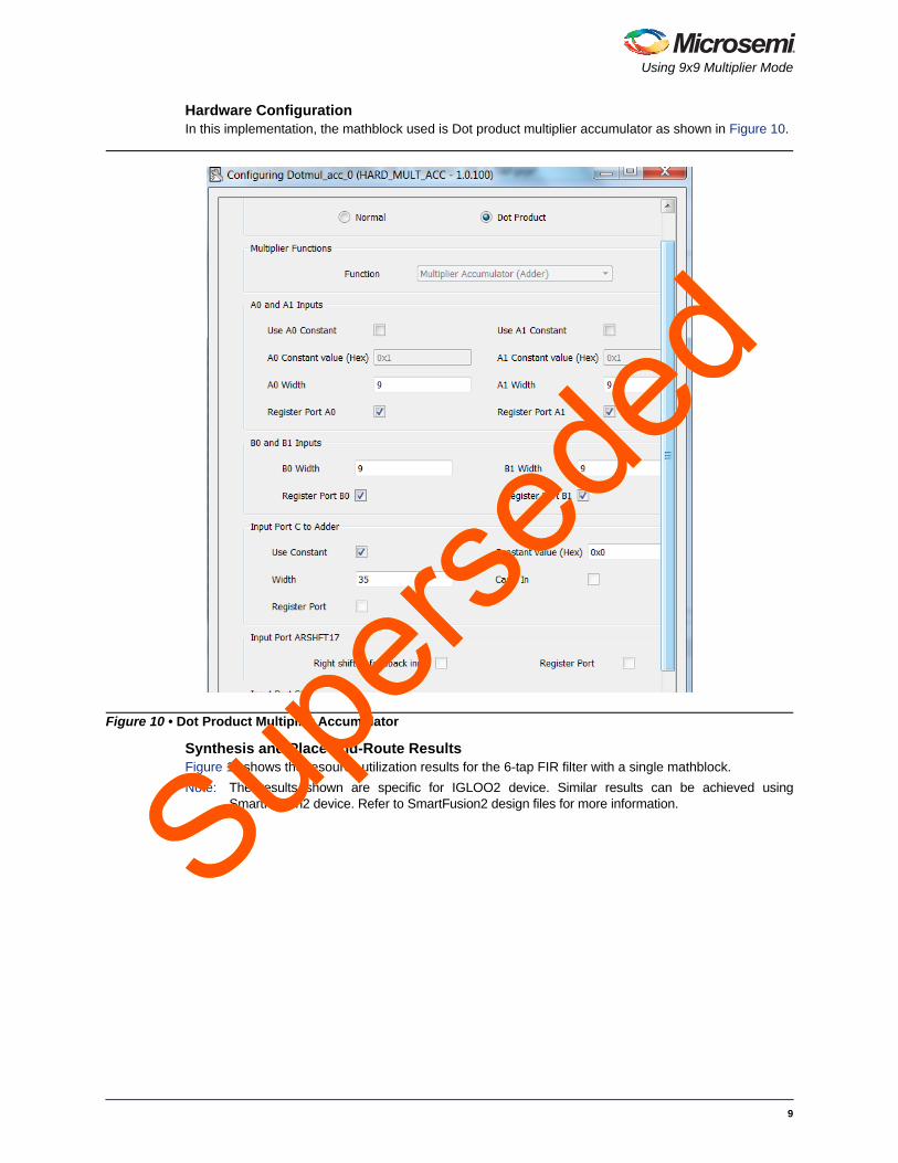
Hardware ConfigurationIn this implementation, the mathblock used is Dot product multiplier accumulator as shown in Figure 10.
Synthesis and Place-and-Route ResultsFigure 11 shows the resource utilization results for the 6-tap FIR filter with a single mathblock.
Note: The results shown are specific for IGLOO2 device. Similar results can be achieved usingSmartFusion2 device. Refer to SmartFusion2 design files for more information.
Figure 10 • Dot Product Multiplier Accumulator
Supers
eded
Supers
eded
9

Implementation of 9x9 Multiplications, Wide-Multiplier, and Extended Addition Using IGLOO2/SmartFusion2 Mathblock
Resource Utilization
Place-and-Route Results
The frequency of operation achieved with this implementation after place-and-route is shown inFigure 12.
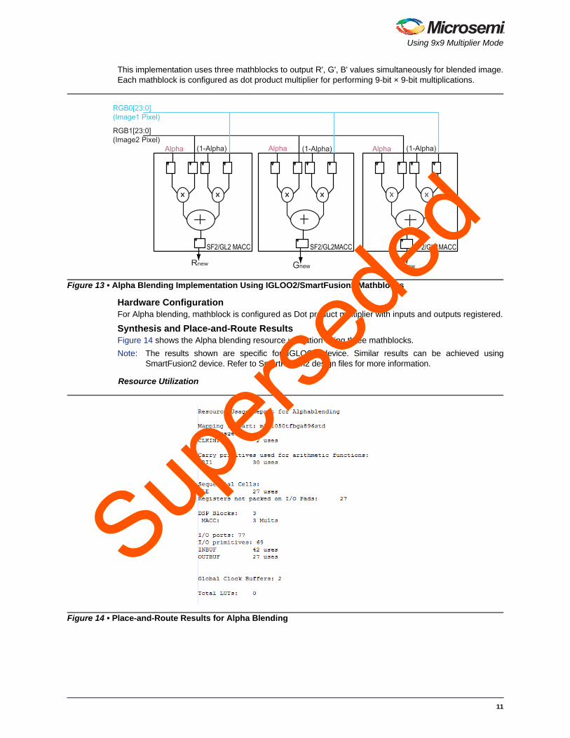
Example 3: Alpha BlendingThe following example shows the implementation of Alpha blending used in image processing as shownin Figure 13 on page 11. Alpha blending is the process of combining a translucent foreground color witha background color, thereby producing a new blended color.
Design DescriptionThe Alpha blending for each Rnew, Gnew, Bnew as shown in Figure 13 on page 11 is implemented usingthe following equations:
Rnew = (1-alpha) x R0 [7:0] + alpha x R1[7:0]
EQ 2
Gnew = (1-alpha) x G0 [7:0] + alpha x G1[7:0]
EQ 3
Bnew = (1-alpha) x B0 [7:0] + alpha x B1[7:0]
EQ 4
Figure 11 • Resource Utilization Results for a Single MAC FIR
Figure 12 • Place-and-Route Results for Single MAC FIR
Supers
eded
Supers
eded
10
Using 9x9 Multiplier Mode
This implementation uses three mathblocks to output R', G', B' values simultaneously for blended image.Each mathblock is configured as dot product multiplier for performing 9-bit × 9-bit multiplications.
Hardware ConfigurationFor Alpha blending, mathblock is configured as Dot product multiplier with inputs and outputs registered.
Synthesis and Place-and-Route ResultsFigure 14 shows the Alpha blending resource utilization using three mathblocks.
Note: The results shown are specific for IGLOO2 device. Similar results can be achieved usingSmartFusion2 device. Refer to SmartFusion2 design files for more information.
Resource Utilization
Figure 13 • Alpha Blending Implementation Using IGLOO2/SmartFusion2 Mathblocks
SF2/GL2 MACC SF2/GL2 MACC SF2/GL2 MACC
Alpha Alpha Alpha(1-Alpha) (1-Alpha) (1-Alpha)
Rnew Gnew Bnew
RGB0[23:0](Image1 Pixel)
RGB1[23:0](Image2 Pixel)
Figure 14 • Place-and-Route Results for Alpha Blending
Supers
eded
Supers
eded
11

Implementation of 9x9 Multiplications, Wide-Multiplier, and Extended Addition Using IGLOO2/SmartFusion2 Mathblock
Place-and-Route Results
The frequency of operation achieved with this implementation after place-and-route is shown inFigure 15.
Wide-Multiplier
OverviewThe wide-multipliers are extensively used in high precision (more than 18×18 multiplication) wireless andmedical applications. These applications require high precision at every stage when implementingcomplex arithmetic functions used in FFT, filters etc. Military, test, and high-performance computing alsorequire performance and precision requirements, and sometimes require single-precision and double-precision floating-point calculations for implementing complex matrix operations and signal transforms.
To implement DSP functions that require high precision, the IGLOO2/SmartFusion2 device offersimplementing wide-multipliers (that is, operands width more than 18×18) with the IGLOO2/SmartFusion2mathblock. The wide-multipliers are implemented by cascading multiple IGLOO2/SmartFusion2mathblocks using CDOUT and CDIN to propagate the result and to achieve the best performanceresults.
This section describes wide-multiplier guidelines and different implementation methods with designexample to achieve the best performance results.
Configuration When implementing the wide-multipliers, the IGLOO2/SmartFusion2 mathblock is configured in Normalmode to function as normal multiplier (18×18), normal multiplier accumulator, and normal multiplieraddsub.
GuidelinesFollowing are some of the important recommendations for implementing wide-multiplier to achieve thebest results.
• The inputs and output are registered with the same clock.
• Add pipeline stages in RTL, so that the synthesis tool can automatically infer registers ofmathblock or register the inputs and outputs of mathblock, if arithmetic cores (Mathblock) areused.
• CDOUT of one mathblock is connected to the CDIN of another mathblock.
Design ExamplesThis section shows the wide-multiplier with the following design examples:
• Multiplier 32×32 implementation using multiple mathblock
• Multiplier 32×32 implementation using single mathblock
The following section explains the 32×32 multiplier implementation with multiple mathblocks and withsingle mathblock. It also shows the performance results for both the implementations.
Figure 15 • Place-and-Route Results for Alpha Blending
Supers
eded
Supers
eded
12
Wide-Multiplier
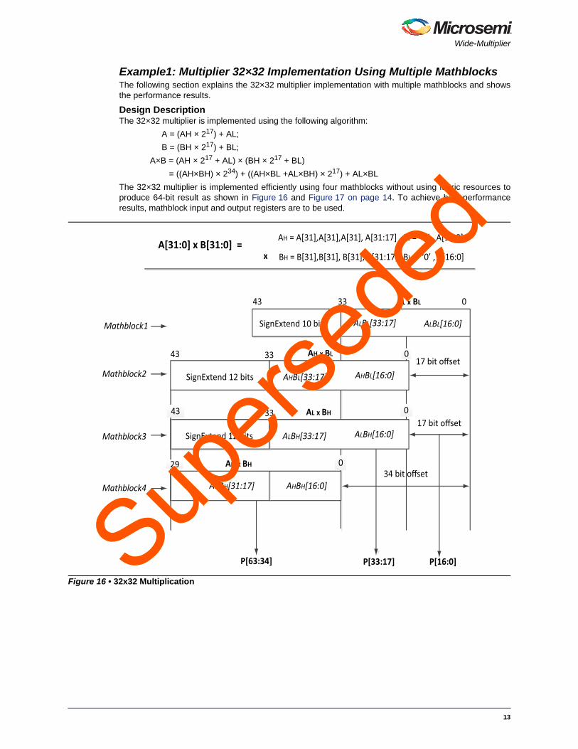
Example1: Multiplier 32×32 Implementation Using Multiple MathblocksThe following section explains the 32×32 multiplier implementation with multiple mathblocks and showsthe performance results.
Design DescriptionThe 32×32 multiplier is implemented using the following algorithm:
A = (AH × 217) + AL;
B = (BH × 217) + BL;
A×B = (AH × 217 + AL) × (BH × 217 + BL)
= ((AH×BH) × 234) + ((AH×BL +AL×BH) × 217) + AL×BL
The 32×32 multiplier is implemented efficiently using four mathblocks without using fabric resources toproduce 64-bit result as shown in Figure 16 and Figure 17 on page 14. To achieve best performanceresults, mathblock input and output registers are to be used.
Figure 16 • 32x32 Multiplication
AL x BL
AH x BH
AH = A[31],A[31],A[31], A[31:17] AL = ‘0’ , A[16:0]
BH = B[31],B[31], B[31], B[31:17] BL = ‘0’ , B[16:0]x
03343
ALBL[33:17] ALBL[16:0]SignExtend 10 bits
033 AL x BH
AHBH[16:0]AHBH[31:17]
AH x BL 03343
AHBL[16:0]AHBL[33:17]SignExtend 12 bits
ALBH[16:0]ALBH[33:17]SignExtend 12 bits
0
P[16:0]P[33:17]P[63:34]
34 bit offset
17 bit offset
17 bit offset
29
43
A[31:0] x B[31:0] =
Mathblock1
Mathblock2
Mathblock3
Mathblock4
Supers
eded
Supers
eded
13

Implementation of 9x9 Multiplications, Wide-Multiplier, and Extended Addition Using IGLOO2/SmartFusion2 Mathblock
When implementing using HDL, to infer mathblock input and output registers by synthesis tool, pipelinestages are added at output and input to achieve maximum throughput. In this design two pipeline stagesare added at input and output. Refer to design files for information on implementation of 32x32 multiplier.
Design Files
For information on the implementation of the multiplier 32×32 design, refer to theMult32×32_multipleMACC.vhd design file provided in <Design files -> Mult32×32_multipleMACC>.
Hardware ConfigurationFor 32×32 multiplier using single mathblock, mathblock is configured to function as normal multiplier,normal multiplier addsub with ARSHFT enabled, inputs and outputs registered.
Normal Multiplier Accumulator —> Pn = Pn-1 + CARRYIN + C +/- A0×B0
Normal Multiplier Addsub —> Pn = D + CARRYIN + C +/- A0×B0 (if ARSHFT is disabled)
—> Pn = (D>>17) + CARRYIN + C +/- A0×B0 (if ARSHFT is enabled)
Normal Multiplier —> P = A0×B0
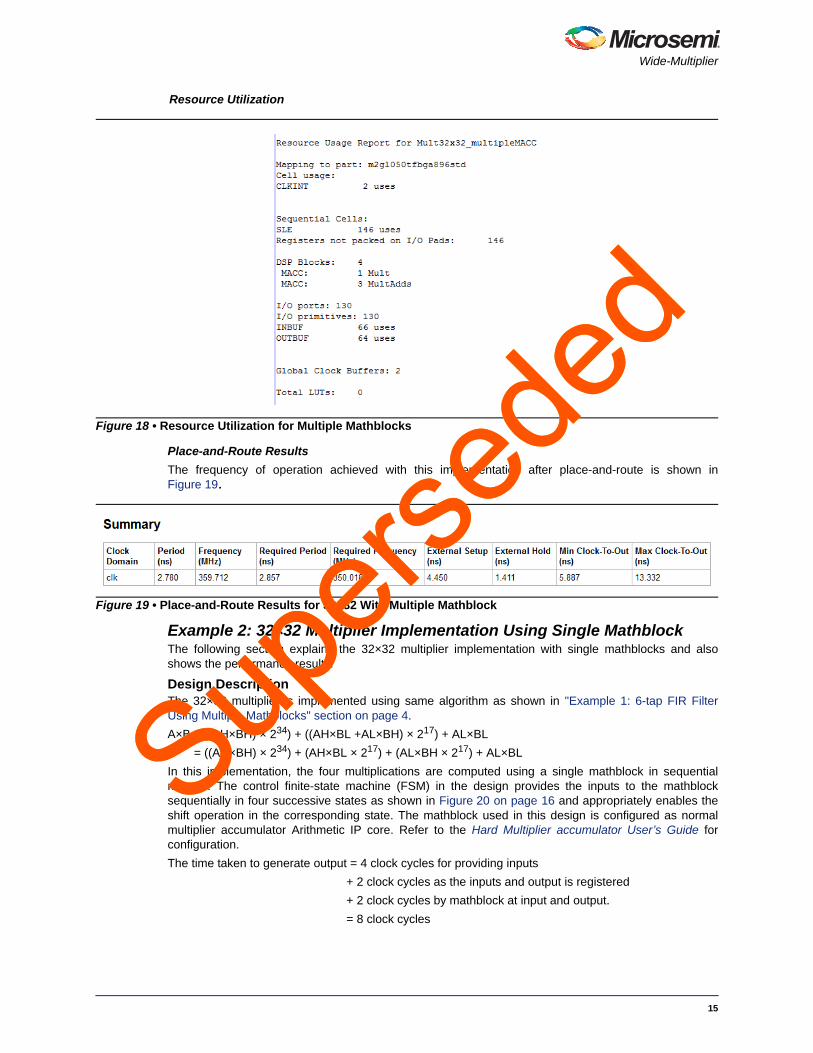
Synthesis and Place-and-Route ResultsFigure 18 on page 15 shows the 32×32 multiplier resource utilization when using multiple mathblocks.
Note: The results shown are specific for IGLOO2 device. Similar results can be achieved usingSmartFusion2 device. Refer to SmartFusion2 design files for more information.
Figure 17 • Implementation of 32x32 Multiplier
Mul�plier 32x32
P[63:34]
Zero’s
SF2/GL2 MACC
AL
SF2/GL2 MACC
17
SF2/GL2 MACC SF2/GL2 MACC
17
P[33:17]P[16:0]
BHALBL AHBL AHBH
Supers
eded
Supers
eded
14
Wide-Multiplier
Resource Utilization
Place-and-Route Results
The frequency of operation achieved with this implementation after place-and-route is shown inFigure 19.
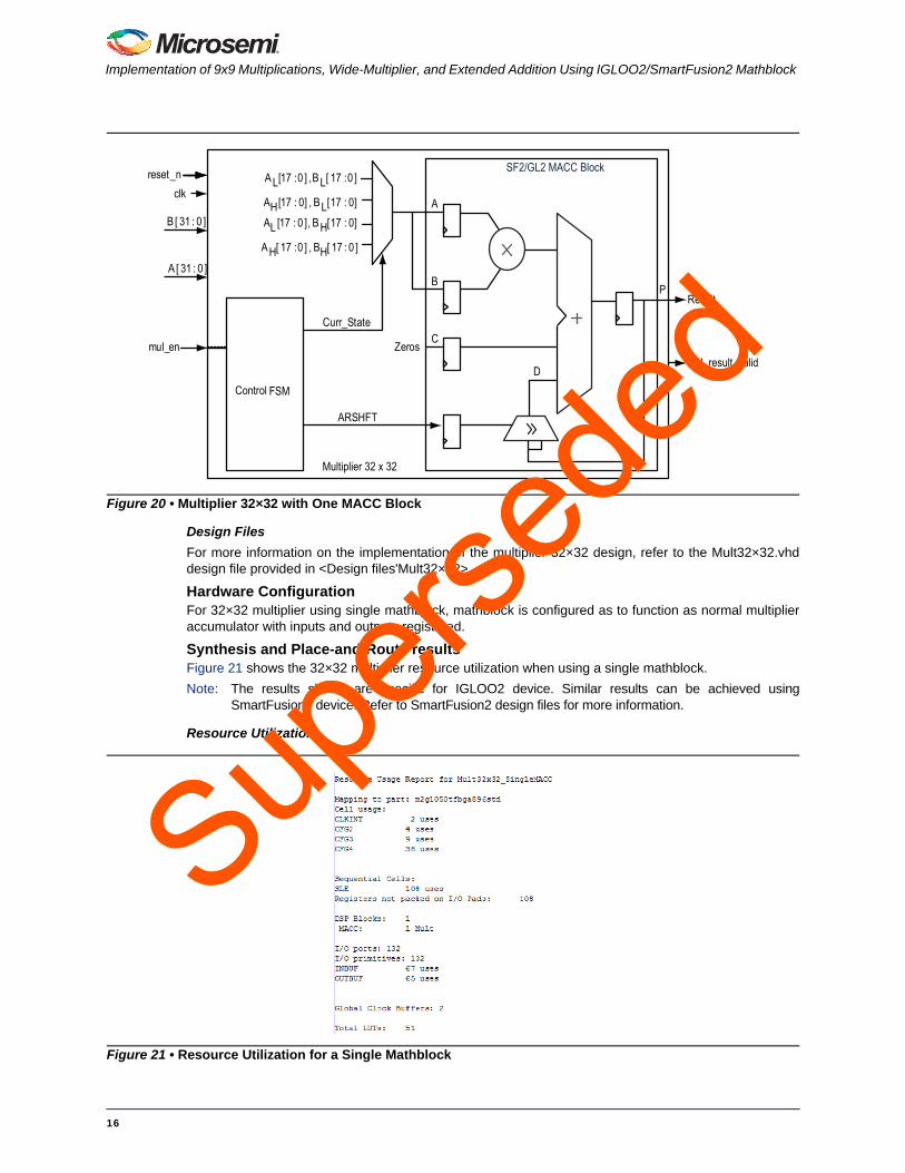
Example 2: 32×32 Multiplier Implementation Using Single MathblockThe following section explains the 32×32 multiplier implementation with single mathblocks and alsoshows the performance results.
Design DescriptionThe 32×32 multiplier is implemented using same algorithm as shown in "Example 1: 6-tap FIR FilterUsing Multiple Mathblocks" section on page 4.
A×B = ((AH×BH) × 234) + ((AH×BL +AL×BH) × 217) + AL×BL
= ((AH×BH) × 234) + (AH×BL × 217) + (AL×BH × 217) + AL×BL
In this implementation, the four multiplications are computed using a single mathblock in sequentialmanner. The control finite-state machine (FSM) in the design provides the inputs to the mathblocksequentially in four successive states as shown in Figure 20 on page 16 and appropriately enables theshift operation in the corresponding state. The mathblock used in this design is configured as normalmultiplier accumulator Arithmetic IP core. Refer to the Hard Multiplier accumulator User’s Guide forconfiguration.
The time taken to generate output = 4 clock cycles for providing inputs
+ 2 clock cycles as the inputs and output is registered
+ 2 clock cycles by mathblock at input and output.
= 8 clock cycles
Figure 18 • Resource Utilization for Multiple Mathblocks
Figure 19 • Place-and-Route Results for 32×32 With Multiple Mathblock
Supers
eded
Supers
eded
15
Implementation of 9x9 Multiplications, Wide-Multiplier, and Extended Addition Using IGLOO2/SmartFusion2 Mathblock
Design Files
For more information on the implementation of the multiplier 32×32 design, refer to the Mult32×32.vhddesign file provided in <Design files'Mult32×32>.
Hardware ConfigurationFor 32×32 multiplier using single mathblock, mathblock is configured as to function as normal multiplieraccumulator with inputs and outputs registered.
Synthesis and Place-and-Route resultsFigure 21 shows the 32×32 multiplier resource utilization when using a single mathblock.
Note: The results shown are specific for IGLOO2 device. Similar results can be achieved usingSmartFusion2 device. Refer to SmartFusion2 design files for more information.
Resource Utilization
Figure 20 • Multiplier 32×32 with One MACC Block
Control FSM
D
C
P
SF2/GL2 MACC BlockA L[17 :0 ] ,BL[ 17 :0 ]
Zeros
Curr_State
ARSHFT
A
B
reset_nclk
mul_en
B [ 31 : 0 ]
A [ 31 : 0 ]
Result
mul_result_valid
AL [17 : 0 ], BH[17 : 0]
AH[17 : 0] , BL[17 : 0]
AH[ 17 :0 ] , BH[ 17 : 0 ]
Multiplier 32 x 32
Figure 21 • Resource Utilization for a Single Mathblock
Supers
eded
Supers
eded
16

Wide-Multiplier
Place-and-Route Results
The frequency of operation achieved with this implementation after place-and-route is shown inFigure 22.
Simulation ResultsFigure 23 shows the post synthesis simulation results. The simulation result shows that the multiplieroutputs on 8 clock cycles after input is provided.
Figure 22 • Place-and-Route Results for 32×32 Multiplier with Single Mathblock
Figure 23 • Multiplier 32×32 Post Synthesis Simulation Results
Supers
eded
Supers
eded
17

Implementation of 9x9 Multiplications, Wide-Multiplier, and Extended Addition Using IGLOO2/SmartFusion2 Mathblock
Extended Addition
OverviewMathblock has a 3-input adder and supports accumulation up to 44 bits. In some applications, such asfloating point multiplication, complex-FFT and filters, high precision data has to be maintained at everystage. These DSP functions require more than 44-bit addition (extended addition) which can be realizedusing the IGLOO2/SmartFusion2 mathblock (3-input adder) and fabric logic. The extended addition isimplemented by dividing the addition into two parts. The lower part (LSB) of addition is implementedusing IGLOO2/SmartFusion2 mathblock and upper part (MSB) of addition is implemented with minimalfabric adder logic.
For a 2-input addition, the inputs can be from any one of the following:
1. CDIN and C input
2. Multiplier output and CDIN
3. Multiplier output and C input
For a 3-input addition, the inputs are from multiplier output, CDIN, and C-input. To perform arithmeticadditions, the IGLOO2/SmartFusion2 mathblock provides Carryin input and Carryout signal forpropagating the carry from one mathblock to another mathblock or from mathblock to fabric logic.
ConfigurationWhen implementing the extended addition, the IGLOO2/SmartFusion2 mathblock is configured inNormal mode to function as normal multiplier addsub.
Guidelines• Mathblock should be configured to function as multiplier adder/subtractor to perform 2-input
extended signed addition.
• Add Pipeline stages in RTL, so that the synthesis tool can automatically infer registers ofmathblock or register the inputs and outputs of mathblock, if arithmetic cores (Mathblock) areused.
• Make sure the CDOUT of one MACC block is connected to the CDIN of another MACC block.
Design ExamplesThis section shows the extended addition with the following design examples:
• 2-input extended signed addition
• 3-input extended signed addition
Example 1: 2-input Signed Extended AdditionThe following section shows a 2-input extended signed addition—if one operand is more than 44-bitwide. In this section, it is also shown that the 2-input extended signed addition implementation logic withfabric resources are implemented with the multiplier adder.Sup
ersed
ed
Supers
eded
18

Extended Addition
Design Description
2-Input Addition
For computing 2-input extended signed addition Z = U + V, with one operand width more than themathblock output width 44, the following logic should be implemented in fabric as shown in Figure 24.
Where U is an m-bit value (where m > 44), V is a sign-extended n-bit value (where n < 44). The 2-inputextended signed addition is divided in two parts. The lower part is computed in the mathblock and theupper part is computed in the fabric.
Z = (Sumupper, Sumlower)
EQ 5
The lower part of the sum, Z = U + V, is calculated by providing the U[(n-1): 0], V[(n-1): 0] inputs tomathblock, where n = 44 is mathblock output width.
Sumlower = U[(n-1): 0] + V[(n-1): 0]
EQ 6
The Upper part of sum Z = U + V is calculated as shown below:
Sumupper = U[m: n] + V[m: n] (where U[m: n], V[m: n] are the MSB bits)
EQ 7
V [m: n] = {S, S….S, X},
S = P[n-1] AND X
Where,P [n-1] is MSB of Sumlower
'X' is the overflow of the Sumlower (from the mathblock)
(m-n-1) number of S's should be appended in MSB bits of the V[m: n].
Hardware ImplementationFigure 25 on page 20 shows the operand width of C as 52-bit wide and explains the implementation for2-input extended signed addition. For 3-input addition, mathblock is configured as multiplier addsub inNormal mode. The upper part and lower part of the sum are shown as follows:For 52-bit, 2-input extended signed addition,
Sumlower = C[43:0] + A[17:0]×B[17:0]
Sumupper = {C[51:44] + {S, S, S, CARRYOUT}}
Result [51:0] = {Sumupper, Sumlower}
Result [51:0] = {C[51:44] + {S, S, S, CARRYOUT}}, P[43:0]Where,S = P[43] AND CARRYOUT
Figure 24 • 2-input Extended Signed Addition
Supers
eded
Supers
eded
19

Implementation of 9x9 Multiplications, Wide-Multiplier, and Extended Addition Using IGLOO2/SmartFusion2 Mathblock
Design Files
For information on the implementation of the 2-input extended addition, refer to theExtended_adder_2_input.vhd design file provided in <Design files'Extended_adder_2_input>.
Synthesis and Place-and-Route ResultsFigure 26 shows the 2-input extended addition resource utilization when using mathblock and fabriclogic.
Note: The results shown are specific for IGLOO2 device. Similar results can be achieved usingSmartFusion2 device. Refer to SmartFusion2 design files for more information.
Resource Utilization with Fabric Adder Logic
Figure 25 • Fabric Logic for 2-input Extended Addition
A[17:0]
B [17:0]
C[43:0]
Result [51:0]
P[43:0]
P[43]
CA
RY
YO
UT
SF2/GL2 MACC
U[8:0] = {S,S,S,S,S,S,X }
X
Fabric Logic for 2-input Adder
C [51:44]
S
Figure 26 • Resource Utilization for 2-input Extended Addition with Fabric Resources
Supers
eded
Supers
eded
20

Extended Addition
Place-and-Route Results with Fabric Adder Logic
The frequency of operation achieved with this implementation after place-and-route is shown inFigure 27.
Simulation ResultsFigure 28 show the post synthesis simulation results. The simulation result shows that the 2-inputaddition outputs on the next clock cycle after the input is provided.
Figure 27 • Place-and-Route Results for 2-input Extended Addition with Fabric Resources
Figure 28 • Post Synthesis Simulation Results for 2-Input Extended Addition with Fabric Adder
Supers
eded
Supers
eded
21
Implementation of 9x9 Multiplications, Wide-Multiplier, and Extended Addition Using IGLOO2/SmartFusion2 Mathblock
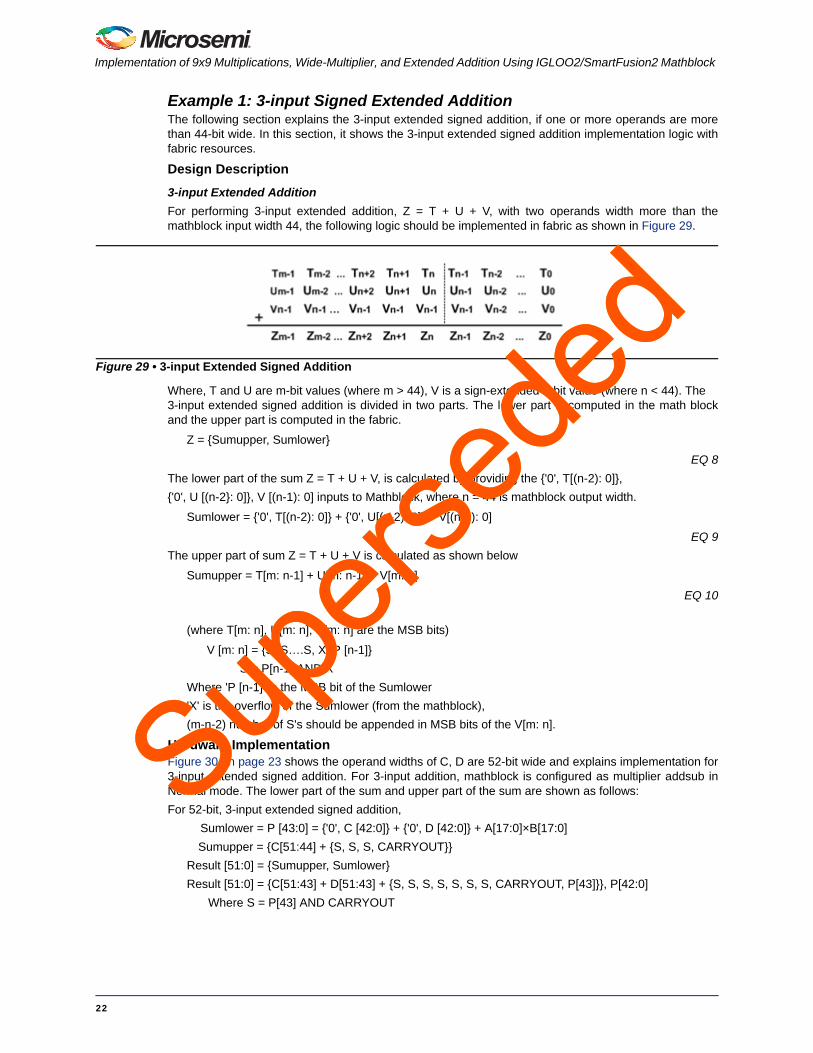
Example 1: 3-input Signed Extended AdditionThe following section explains the 3-input extended signed addition, if one or more operands are morethan 44-bit wide. In this section, it shows the 3-input extended signed addition implementation logic withfabric resources.
Design Description
3-input Extended Addition
For performing 3-input extended addition, Z = T + U + V, with two operands width more than themathblock input width 44, the following logic should be implemented in fabric as shown in Figure 29.
Where, T and U are m-bit values (where m > 44), V is a sign-extended n-bit value (where n < 44). The 3-input extended signed addition is divided in two parts. The lower part is computed in the math blockand the upper part is computed in the fabric.
Z = {Sumupper, Sumlower}
EQ 8
The lower part of the sum Z = T + U + V, is calculated by providing the {'0', T[(n-2): 0]},
{'0', U [(n-2}: 0]}, V [(n-1): 0] inputs to Mathblock, where n = 44 is mathblock output width.
Sumlower = {'0', T[(n-2): 0]} + {'0', U[(n-2): 0]} + V[(n-1): 0]
EQ 9
The upper part of sum Z = T + U + V is calculated as shown below
Sumupper = T[m: n-1] + U[m: n-1] + V[m: n]
EQ 10
(where T[m: n], U[m: n], V[m: n] are the MSB bits)
V [m: n] = {S, S….S, X, P [n-1]}
S = P[n-1] AND X
Where 'P [n-1]' is the MSB bit of the Sumlower
'X' is the overflow of the Sumlower (from the mathblock),
(m-n-2) number of S's should be appended in MSB bits of the V[m: n].
Hardware ImplementationFigure 30 on page 23 shows the operand widths of C, D are 52-bit wide and explains implementation for3-input extended signed addition. For 3-input addition, mathblock is configured as multiplier addsub inNormal mode. The lower part of the sum and upper part of the sum are shown as follows:
For 52-bit, 3-input extended signed addition,
Sumlower = P [43:0] = {'0', C [42:0]} + {'0', D [42:0]} + A[17:0]×B[17:0]
Sumupper = {C[51:44] + {S, S, S, CARRYOUT}}
Result [51:0] = {Sumupper, Sumlower}
Result [51:0] = {C[51:43] + D[51:43] + {S, S, S, S, S, S, S, CARRYOUT, P[43]}}, P[42:0]
Where S = P[43] AND CARRYOUT
Figure 29 • 3-input Extended Signed Addition
Supers
eded
Supers
eded
22
Extended Addition
Design Files For further information on how to implement the 3-input extended addition, refer to theExtended_adder_3_input.vhd design file provided in <Design files'Extended_adder_3_input>.
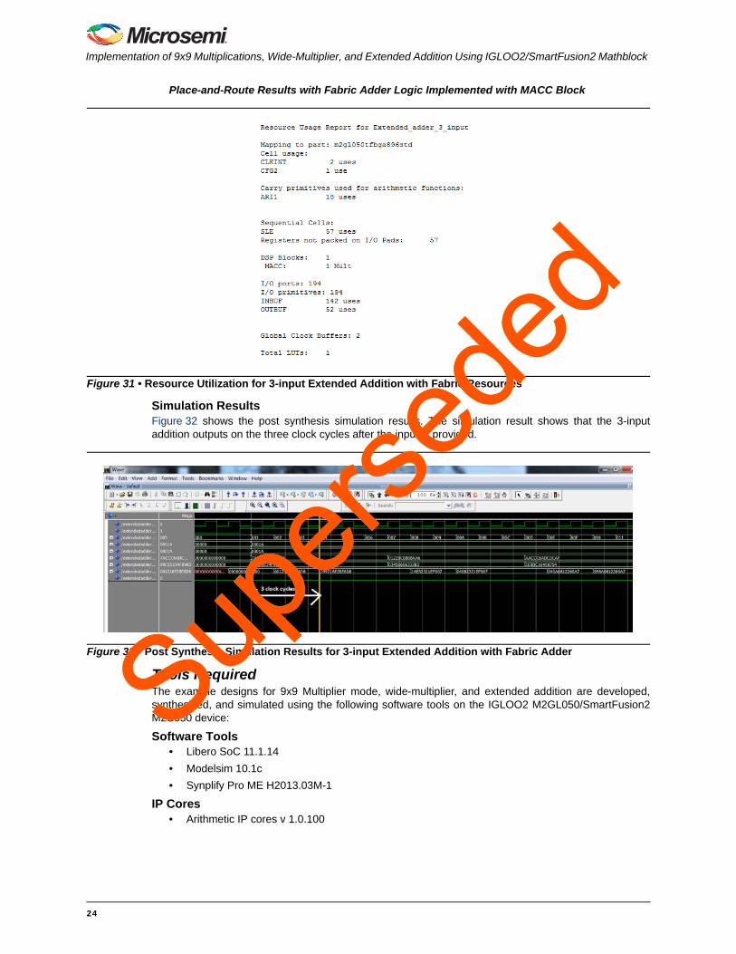
Synthesis and Place-and-Route ResultsFigure 31 shows the 3-input extended addition resource utilization when using fabric logic.
Note: The results shown are specific for IGLOO2 device. Similar results can be achieved usingSmartFusion2 device. Refer to SmartFusion2 design files for more information.
Figure 30 • Fabric Logic for 3-input Extended Addition
A[17:0]
B [17:0]
‘0’,C[42:0]
‘0’,D [42:0]
Result [51:0]
P[43:0]
P[43]
CA
RR
YO
UT
SF2/GL2 MACC
U[8:0] = {S,S,S,S,S,S,X,P[43]}
X
D [51:44]
Fabric Logic for 3-input Adder
C [51:44]
S
P[43]
Supers
eded
Supers
eded
23
Implementation of 9x9 Multiplications, Wide-Multiplier, and Extended Addition Using IGLOO2/SmartFusion2 Mathblock
Place-and-Route Results with Fabric Adder Logic Implemented with MACC Block
Simulation ResultsFigure 32 shows the post synthesis simulation results. The simulation result shows that the 3-inputaddition outputs on the three clock cycles after the input is provided.
Tools RequiredThe example designs for 9x9 Multiplier mode, wide-multiplier, and extended addition are developed,synthesized, and simulated using the following software tools on the IGLOO2 M2GL050/SmartFusion2M2S050 device:
Software Tools• Libero SoC 11.1.14
• Modelsim 10.1c
• Synplify Pro ME H2013.03M-1
IP Cores• Arithmetic IP cores v 1.0.100
Figure 31 • Resource Utilization for 3-input Extended Addition with Fabric Resources
Figure 32 • Post Synthesis Simulation Results for 3-input Extended Addition with Fabric Adder
Supers
eded
Supers
eded
24

ConclusionThis application notes explains IGLOO2/SmartFusion2 mathblock features such as 9x9 Multiplier mode,wide-multiplier, and extended addition. This document also provides implementation techniques andguidelines along with the design examples for the 9x9 Multiplication, wide-multiplier, and extendedaddition for optimum performance.
Appendix A - Design FilesDownload the design files (VHDL) from the Microsemi SoC Products Group website:www.microsemi.com/soc/download/rsc/?f=DSPAN_GL2_DF.
www.microsemi.com/soc/download/rsc/?f=DSPAN_SF2_DF. Refer to the Readme.txt file included in the design file for the directory structure and description.
Supers
eded
Supers
eded

51900274-0/06.13
© 2013 Microsemi Corporation. All rights reserved. Microsemi and the Microsemi logo are trademarks ofMicrosemi Corporation. All other trademarks and service marks are the property of their respective owners.
Microsemi Corporation (NASDAQ: MSCC) offers a comprehensive portfolio of semiconductorsolutions for: aerospace, defense and security; enterprise and communications; and industrialand alternative energy markets. Products include high-performance, high-reliability analog andRF devices, mixed signal and RF integrated circuits, customizable SoCs, FPGAs, andcomplete subsystems. Microsemi is headquartered in Aliso Viejo, Calif. Learn more atwww.microsemi.com.
Microsemi Corporate HeadquartersOne Enterprise, Aliso Viejo CA 92656 USAWithin the USA: +1 (949) 380-6100Sales: +1 (949) 380-6136Fax: +1 (949) 215-4996
Supers
eded
Supers
eded