implementation of a 1×2 optical power splitter based on 2-d square … · on 2-d square-lattice...
TRANSCRIPT

International Research Journal of Applied and Basic Sciences © 2013 Available online at www.irjabs.com ISSN 2251-838X / Vol, 4 (2): 296-301 Science Explorer Publications
Implementation of a 1×2 Optical Power Splitter based
on 2-D Square-Lattice PCRR for the 3rd Optical Communication Band
Alireza Tavousi1, Mojtaba Moradi2, and Mohammad Ali Mansouri-Birjandi2
1. Faculty of Electrical and Computer Engineering, University of Tabriz, Tabriz, Iran 2. Faculty of Electrical and Computer Engineering, University of Sistan and Baluchestan, Zahedan, Iran
Corresponding author email: [email protected]
ABSTRACT: In this article, we propose a 1 × 2 optical power splitter made of ring resonators and linear-defect waveguides in photonic crystals. This structure is based on a square lattice of silicon rods with the refractive index n1=3.47 surrounded by air (with refractive index n2=1). The broadest photonic band gap for this lattice occurs at the optimized filling ratio of r/a = 0.2. Our proposed power splitter is formed by the appropriate coupling distance between two mirrored rings and a linear defect W1 waveguide. Due to constructive interferences in ring resonators which cause the intensity inside the ring builds up in over several round-trips, the splitting efficiency of power splitter is found to be near %60 in each arm with a FWHM of 21nm – from 1.541~1.564�m. This intensity corresponds to a hexa-pole degenerated resonant mode which its normalized frequencies are 0.3480 and 0.3483 (a/�). Resonance modes of the ring resonator with their corresponding degenerated poles and the transmission spectra are calculated using the PWE, and 2D-FDTD methods respectively. Keywords: Photonic Crystal; PCRR; Power Splitter; Ring Resonator.
INTRODUCTION The current optoelectronic devices are expected to work at up 100 Gbit/s (Yariv, 1997). Beyond that speed, pure all-optical devices are needed (Gibbs, 1985). Such devices can be achieved by using the photonic crystal (PC) technology (Busch, 2004; Lourtioz, 2005) that is one of the most important scientific areas with a huge industrial potential. The field of PCs is experiencing an extraordinary growth due to the dramatic ways in which such structures can control, modify, and harvest the flow of light (Badaoui et al., 2011; Dorrani and Mansouri-Birjandi, 2012; Skorobogatiy and Yang, 2009). One of the main advantages of the PC technology is the possibility of the full integration of optical devices on all-optical chips that can operate at much higher frequency and consume less power than today's electronic silicon chips (Maksymov, 2010). By introducing defects (point, line, etc) in PCs perfect lattice, defect modes in their PBGs is formed (Ghaffari et al., 2009; Ghaffari et al., 2008). Photonic crystal waveguides (PCWs) are one of the key components of PCs, which are constructed by introducing linear defects into perfect PCs. PCWs confirm that there is no radiation loss through sharp bends in PCWs (Fan et al., 2001). The size of the devices based on PCWs can be reduced significantly compared with their conventional counterparts. The optical power splitter or divider is a vital element in photonic integrated circuits (PICs) which is used in fiber optic networks. Basic structure of the splitter is divided into two parts, an input and an output port. Ideally, input power is equally divided into the output ports without any considerable reflection and radiation loss and must be compact in size (Chung and Yoon, 2003). There are multiple ways by which equal amount of power of incoming powers or signals can be separated into two, three or four output channels; for example using multiple coupled PCWs, directional coupling and cascaded multimode PCWs. To decrease the multimode problem and bending loss, several researchers investigated theoretically an array of dielectric rods in air. The advantage of this structure

Intl. Res. J. Appl. Basic. Sci. Vol., 4 (2), 296-301, 2013
297
is the waveguide created by removing a single line of rods is single mode and light propagates in the region of the sharp bends with high transmission value. Based on this concept the T-junction, Y-junction and multiple coupled PCWs have already been investigated (Rakhshani and Mansouri-Birjandi, 2012; Yu et al., 2008). The PC ring resonators (PCRRs) can be considered as a new type of linear defects which their size is determined by the desired resonant wavelength. In comparison with point or linear defect, for reasons such as scalability in size and having many design parameters such as scattering rods radius, distance between the rods and the refractive index of the structure, PCRRs offer better flexibility and adaptability in the structure design (Robinson and Nakkeeran, 2011, 2012). Since Si material provides a wide PBG for its large refractive index difference with air (Inoue and Ohtaka, 2004; Joannopoulos et al., 2008; Tavousi et al., 2012) it is selected as the first-choice material used in the present paper. The desired wavelength performance window is located within the third optical telecommunications window (1.53~1.565�m). Using plane wave expansion (PWE) and two dimensional finite difference time domain (2D FDTD) computations, the structure is analyzed numerically, and it is confirmed that over 60% of transmission efficiency through each output channel is achieved. This paper’s organization is as follow: in the second part of the paper, we discuss the design procedures of our power splitter. We discuss about the simulation results in Section III and in the last section, we express the conclusions.
NUMERICAL ANALYSIS AND DISCUSSION The system under consideration is an array of rods with a two-dimensional square lattice. The refractive index of silicon rods is n1=3.47 and the environment is air with refractive index n2=1. The number of rods in the x-z plane is 15 × 25.
Figure 1 shows the schematic representation of the proposed power splitter implemented on 2D PC with a square lattice. The splitter structure consists of 3 parts. First the input waveguide formed by a W1 defect waveguide (a single line defect in the �X direction) directly coupled to the ring resonator. The PCRR is the second and main part of the splitter which has a complicated design. The third and last part of our splitter is the 90 degree bend waveguide coupled to the bottom of the ring.
Figure 1.Geometry of the proposed 1×2 splitting structure.
Design and Optimization of PC Perfect Lattice
Figure 2(a) shows the PC’s PBG which is calculated for r/a=0.2 using PWE method with TM polarization mode. The ‘X’ axis represents the line connecting points of first Brillion zone (the smallest periodical space in the lattice structure) and ‘Z’ axis shows the normalized frequency �a/2�c = a/� where ‘�’ is the angular frequency, ‘a’ is the lattice constant (distance between centers of two adjacent rods), ‘c’ is the light speed in the vacuum and ‘�’ is the free space wavelength. The existence of PBG for TM mode in the first two bands is clearly visible in this figure. In the upper half of the PBG, radiation and leaky modes coexist, Therefore we mainly focus on the performance of the

Intl. Res. J. Appl. Basic. Sci. Vol., 4 (
structuresobtains as polarization, wefor it,the normalized gap width is
Figurewith PWE method using the supercell of 7boundary conditions (ABC) which is deformedwavesymmetry point.
PCRRs Design and Optimization output) to the ring through evanescent coupling modes and due to constructive interference its intensity builds up in over several roundwaveguide. Since only some wavelengths resonate within the ring, it somehow functions as a filter. there is also a much higher intensity in the waveguide region. Such intenexponentially outside of the waveguide region
Intl. Res. J. Appl. Basic. Sci. Vol., 4 (
structures in the lower part of the PBG. obtains as a=0.54 To find the best rod’s radii for which the PBG is maximum inpolarization, wefor it, obtains for the normalized gap width is The light is guided toward the PCRR through a W1 waveguide. In
Figure 2(b), the waveguide dispersion curve is depicted. with PWE method using the supercell of 7boundary conditions (ABC) which is We obtained the waveguide guideddeformed lattice (lattice with linear defect W1 waveguide)wave numberssymmetry point.
Figure 2. (a)
PCRRs Design and Optimization PCRRoutput) waveguides. When light with the appropriate wavelength is launched to the input waveguide, it will couple to the ring through evanescent coupling modes and due to constructive interference its intensity builds up in over several roundwaveguide. Since only some wavelengths resonate within the ring, it somehow functions as a filter. there is also a much higher intensity in the waveguide region. Such intenexponentially outside of the waveguide region
Figure
Intl. Res. J. Appl. Basic. Sci. Vol., 4 (
in the lower part of the PBG. =0.54�m. Also the PBG’s corresponding
To find the best rod’s radii for which the PBG is maximum inpolarization, we draw the gap
obtains for r/a = 0.2. the normalized gap width is �
The light is guided toward the PCRR through a W1 waveguide. In
, the waveguide dispersion curve is depicted. with PWE method using the supercell of 7boundary conditions (ABC) which is
We obtained the waveguide guidedlattice (lattice with linear defect W1 waveguide)
numbers. The beginning ofsymmetry point.
(a) Photonic crystal perfect
PCRRs Design and OptimizationPCRR consist of a quasiwaveguides. When light with the appropriate wavelength is launched to the input waveguide, it will couple
to the ring through evanescent coupling modes and due to constructive interference its intensity builds up in over -trips and emits almos
waveguide. Since only some wavelengths resonate within the ring, it somehow functions as a filter. there is also a much higher intensity in the waveguide region. Such intenexponentially outside of the waveguide region
Figure 3. The 3x3 PCRR
Intl. Res. J. Appl. Basic. Sci. Vol., 4 (2), 2
in the lower part of the PBG. . Also the PBG’s corresponding
To find the best rod’s radii for which the PBG is maximum indraw the gap map in terms of
. The normalizedthe normalized gap width is ��a/2�c�0.143
The light is guided toward the PCRR through a W1 waveguide. In
, the waveguide dispersion curve is depicted. with PWE method using the supercell of 7boundary conditions (ABC) which is shown in the subset of
We obtained the waveguide guidedlattice (lattice with linear defect W1 waveguide)
beginning of the guided
Photonic crystal perfect lattice frequency band structure for T
PCRRs Design and Optimization consist of a quasi-circular waveguide in a closed loop side
waveguides. When light with the appropriate wavelength is launched to the input waveguide, it will couple to the ring through evanescent coupling modes and due to constructive interference its intensity builds up in over
trips and emits almost whole of it in the drop waveguide. Then it can be grabbed by a pick waveguide. Since only some wavelengths resonate within the ring, it somehow functions as a filter. there is also a much higher intensity in the waveguide region. Such intenexponentially outside of the waveguide region
The 3x3 PCRR structure with
296-301, 2013
in the lower part of the PBG. For the desired wavelength and the chosen rod’s radii,. Also the PBG’s corresponding
To find the best rod’s radii for which the PBG is maximum inin terms of filling ratio (
normalized frequency0.143.
The light is guided toward the PCRR through a W1 waveguide. In
, the waveguide dispersion curve is depicted. with PWE method using the supercell of 7a×1a dimension and
shown in the subset of We obtained the waveguide guided mode
lattice (lattice with linear defect W1 waveguide)guided mode (red
lattice frequency band structure for Twaveguide in
circular waveguide in a closed loop sidewaveguides. When light with the appropriate wavelength is launched to the input waveguide, it will couple
to the ring through evanescent coupling modes and due to constructive interference its intensity builds up in over t whole of it in the drop waveguide. Then it can be grabbed by a pick
waveguide. Since only some wavelengths resonate within the ring, it somehow functions as a filter. there is also a much higher intensity in the waveguide region. Such intenexponentially outside of the waveguide region (Joannopoulos et al, 2008).
structure with the chosen
, 2013
For the desired wavelength and the chosen rod’s radii, wavelength range
To find the best rod’s radii for which the PBG is maximum infilling ratio (r/a). The
frequency range corresponding to
The light is guided toward the PCRR through a W1 waveguide. In
, the waveguide dispersion curve is depicted. The dispersion curve for the input waveguide is computed dimension and Beranger’s perfectly matche
shown in the subset of this figure by collating the
lattice (lattice with linear defect W1 waveguide), in the red line) is from the
lattice frequency band structure for T
waveguide in �-X direction.
circular waveguide in a closed loop sidewaveguides. When light with the appropriate wavelength is launched to the input waveguide, it will couple
to the ring through evanescent coupling modes and due to constructive interference its intensity builds up in over t whole of it in the drop waveguide. Then it can be grabbed by a pick
waveguide. Since only some wavelengths resonate within the ring, it somehow functions as a filter. there is also a much higher intensity in the waveguide region. Such inten
nopoulos et al, 2008).
the chosen super cell for calculating the resonan
For the desired wavelength and the chosen rod’s radii,range is 1.297~1.925
To find the best rod’s radii for which the PBG is maximum in the TM (The best filling
corresponding to
The light is guided toward the PCRR through a W1 waveguide. In
The dispersion curve for the input waveguide is computed Beranger’s perfectly matche
this figure. collating the dispersion
space of irreducible) is from the normalized
lattice frequency band structure for TM polarization mode.direction.
circular waveguide in a closed loop side-coupled to one or more bus (or inputwaveguides. When light with the appropriate wavelength is launched to the input waveguide, it will couple
to the ring through evanescent coupling modes and due to constructive interference its intensity builds up in over t whole of it in the drop waveguide. Then it can be grabbed by a pick
waveguide. Since only some wavelengths resonate within the ring, it somehow functions as a filter. there is also a much higher intensity in the waveguide region. Such intensities are called evanescent as they decay
nopoulos et al, 2008).
super cell for calculating the resonan
For the desired wavelength and the chosen rod’s radii,is 1.297~1.925�m.
(electric field filling ratio that the broadest PBG occurs
this ratio is 0.296
The dispersion curve for the input waveguide is computed Beranger’s perfectly matched layer (PML) absorbing
dispersion diagrams irreducible Brillion zone
normalized frequency
polarization mode. (b) Dispersion curve of W1
coupled to one or more bus (or inputwaveguides. When light with the appropriate wavelength is launched to the input waveguide, it will couple
to the ring through evanescent coupling modes and due to constructive interference its intensity builds up in over t whole of it in the drop waveguide. Then it can be grabbed by a pick
waveguide. Since only some wavelengths resonate within the ring, it somehow functions as a filter. sities are called evanescent as they decay
super cell for calculating the resonan
For the desired wavelength and the chosen rod’s radii, the lattice constant
electric field parallel to the rodratio that the broadest PBG occurs
0.296 � a/� � 0.439
The dispersion curve for the input waveguide is computed d layer (PML) absorbing
of the perfectBrillion zone for normalized
frequency a/�=0.308 in the
(b) Dispersion curve of W1
coupled to one or more bus (or inputwaveguides. When light with the appropriate wavelength is launched to the input waveguide, it will couple
to the ring through evanescent coupling modes and due to constructive interference its intensity builds up in over t whole of it in the drop waveguide. Then it can be grabbed by a pick
waveguide. Since only some wavelengths resonate within the ring, it somehow functions as a filter. At resonance, sities are called evanescent as they decay
super cell for calculating the resonanc modes.
298
the lattice constant
the rod axis) ratio that the broadest PBG occurs
� 0.439 and
The dispersion curve for the input waveguide is computed d layer (PML) absorbing
perfect and the normalized
=0.308 in the k=�
(b) Dispersion curve of W1
coupled to one or more bus (or input-waveguides. When light with the appropriate wavelength is launched to the input waveguide, it will couple
to the ring through evanescent coupling modes and due to constructive interference its intensity builds up in over t whole of it in the drop waveguide. Then it can be grabbed by a pick
At resonance, sities are called evanescent as they decay

Intl. Res. J. Appl. Basic. Sci. Vol., 4 (2), 296-301, 2013
299
Figure 3 shows structure of our designed and optimized 3x3 PCRR. Four scattering rods, which are the same as other rods and are indicated with label (Scaterer) have been added in the corners of the PCRR and on the center of the imaginary square made by its four adjacent rods. These rods act like a wavelength reflector, so they will decrease back reflections in the corresponding corners. This PCRR has a lot of different resonance modes, naming them as mono-pole, di-pole, tetra-pole, hexa-pole, octa-pole, daca-pole and etc. For most of the cases monopole mode is alone but others are degenerate with a phase shift 180 degree divided by number of pole (Fan et al., 1998; Qiang et al., 2007). For calculating the PCRR resonance modes, a 7a × 7a supercell is selected. The optimal number of bands needed for calculation of the PCRR near-filed pattern using equation (1) is suggested to be 7 × (2+7) = 63. This equation is suggested by Fan et al. (Fan et al., 1998). In this equation x and y are the supercell dimensions.
( ) ( )[ ]yxMaxyxMinNumber ,(2),( ×+= (1)
Figure 4 shows the near-filed patterns of the proposed PCRR. Theses modes have been calculated using PWE method for the |Ey|
2 field component for the symmetry point k=� in TM polarization mode. The main
resonance mode of the proposed PCRR which resonate in the �-K direction is a hexa-pole with two degenerate states and 30 degree phase shift between them. Normalized frequencies corresponding to this degenerated hexa-pole are a/�=0.48066 and 0.348301.
Figure 4. The near-filed patterns of the proposed PCRR. normalized frequencies the main resonant modes of PCRR in �-X direction are 0.348066 and 0.348301.
SIMULATION RESULTS
Intl. Res. J. Appl. Basic. Sci. Vol., 4 (
with PML ABCs. The FDTD mesh size and time step are space).function multiplying a sinusoidal carrier with 2excite the fundamental waveguide mode and PCRR’s evanescent resonan frequency analysis which is based on analysis is calculated forspectrawavelength.a single wavelength i.e. on or off thewaveguide is completely
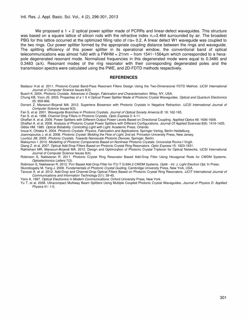
power. The full transmfrom 1.541~1.564
Intl. Res. J. Appl. Basic. Sci. Vol., 4 (
The transmission spectra with PML ABCs. The FDTD mesh size and time step are space). To obtain the time response of the power splitter, a pulse excifunction multiplying a sinusoidal carrier with 2excite the fundamental waveguide mode and PCRR’s evanescent resonan Since we desire thfrequency analysis which is based on analysis is calculated forspectra are calculated wavelength. A continues wave (CW) Gaussian excitation source is used to simulate the powera single wavelength i.e. on or off Figure the best output peak occurs atwaveguide is completely
In Figure power. The full transmfrom 1.541~1.564
Figure 6. (a)
Intl. Res. J. Appl. Basic. Sci. Vol., 4 (
The transmission spectra with PML ABCs. The FDTD mesh size and time step are
To obtain the time response of the power splitter, a pulse excifunction multiplying a sinusoidal carrier with 2excite the fundamental waveguide mode and PCRR’s evanescent resonan
Since we desire thfrequency analysis which is based on analysis is calculated for Gaussian pulse
are calculated asA continues wave (CW) Gaussian excitation source is used to simulate the power
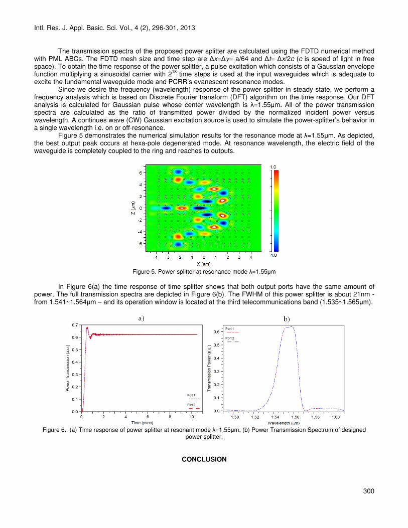
a single wavelength i.e. on or offFigure 5 demonstrates the output peak occurs at
waveguide is completely coupled
Figure 6(a) the time response of time splitter shows that both output ports have the same amount of power. The full transmission spectrfrom 1.541~1.564�m – and its operation window is located at
(a) Time response of power splitter at resonant mode
Intl. Res. J. Appl. Basic. Sci. Vol., 4 (2), 2
The transmission spectra of the proposed power splitter with PML ABCs. The FDTD mesh size and time step are
To obtain the time response of the power splitter, a pulse excifunction multiplying a sinusoidal carrier with 2excite the fundamental waveguide mode and PCRR’s evanescent resonan
Since we desire the frequency (wavelength) response of the power splitter in steady statefrequency analysis which is based on D
Gaussian pulse as the ratio of transmitted power
A continues wave (CW) Gaussian excitation source is used to simulate the powera single wavelength i.e. on or off-resonance.
demonstrates the numericaloutput peak occurs at hexa-pole
coupled to the ring and reaches
Figure 5
) the time response of time splitter shows that both output ports have the same amount of ission spectra areand its operation window is located at
Time response of power splitter at resonant mode
296-301, 2013
of the proposed power splitter with PML ABCs. The FDTD mesh size and time step are
To obtain the time response of the power splitter, a pulse excifunction multiplying a sinusoidal carrier with 2
18 time steps is used at the input waveguides which is adequate to
excite the fundamental waveguide mode and PCRR’s evanescent resonane frequency (wavelength) response of the power splitter in steady state
Discrete FourierGaussian pulse whose center
the ratio of transmitted power A continues wave (CW) Gaussian excitation source is used to simulate the power
resonance. numerical simulation results
pole degeneratedto the ring and reaches
5. Power splitter at
) the time response of time splitter shows that both output ports have the same amount of are depicted in
and its operation window is located at
Time response of power splitter at resonant mode power splitter.
CONCLUSION
, 2013
of the proposed power splitter are calculated using the FDTD numerical method with PML ABCs. The FDTD mesh size and time step are �x=�y
To obtain the time response of the power splitter, a pulse excitime steps is used at the input waveguides which is adequate to
excite the fundamental waveguide mode and PCRR’s evanescent resonane frequency (wavelength) response of the power splitter in steady state
Fourier transform (DFT) algorithmwhose center wavelength is
the ratio of transmitted power divided byA continues wave (CW) Gaussian excitation source is used to simulate the power
simulation results fordegenerated mode. At resonance wavelength, the electric field of the
to the ring and reaches to outputs.
plitter at resonance
) the time response of time splitter shows that both output ports have the same amount of depicted in Figure 6(b). Th
and its operation window is located at the third telecommunications band (1.535~1.565
Time response of power splitter at resonant mode �=1.55power splitter.
CONCLUSION
are calculated using the FDTD numerical method y= a/64 and �
To obtain the time response of the power splitter, a pulse excitation which consists of a Gaussian envelope time steps is used at the input waveguides which is adequate to
excite the fundamental waveguide mode and PCRR’s evanescent resonance modes.e frequency (wavelength) response of the power splitter in steady state
transform (DFT) algorithmwavelength is �=1.55
divided by the A continues wave (CW) Gaussian excitation source is used to simulate the power
for the resonance. At resonance wavelength, the electric field of the
to outputs.
ce mode �=1.55�
) the time response of time splitter shows that both output ports have the same amount of . The FWHM of this power splitter
the third telecommunications band (1.535~1.565
=1.55�m. (b) Power Transmission Spectrum of designed
are calculated using the FDTD numerical method = a/64 and �t= �x/2c (c is
tation which consists of a Gaussian envelope time steps is used at the input waveguides which is adequate to
modes. e frequency (wavelength) response of the power splitter in steady state
transform (DFT) algorithm on the time response=1.55�m. All of the power transmission the normalized
A continues wave (CW) Gaussian excitation source is used to simulate the power
the resonance mode at �. At resonance wavelength, the electric field of the
=1.55�m
) the time response of time splitter shows that both output ports have the same amount of of this power splitter
the third telecommunications band (1.535~1.565
. (b) Power Transmission Spectrum of designed
are calculated using the FDTD numerical method is speed of light in free
tation which consists of a Gaussian envelope time steps is used at the input waveguides which is adequate to
e frequency (wavelength) response of the power splitter in steady state, we perform a on the time response
the power transmission incident power versus
A continues wave (CW) Gaussian excitation source is used to simulate the power-splitter’s behavior in
at �=1.55�m. As . At resonance wavelength, the electric field of the
) the time response of time splitter shows that both output ports have the same amount of of this power splitter is about 21nm
the third telecommunications band (1.535~1.565
. (b) Power Transmission Spectrum of designed
300
are calculated using the FDTD numerical method speed of light in free
tation which consists of a Gaussian envelope time steps is used at the input waveguides which is adequate to
, we perform a on the time response. Our DFT
the power transmission incident power versus
er’s behavior in
. As depicted, . At resonance wavelength, the electric field of the
) the time response of time splitter shows that both output ports have the same amount of is about 21nm -
the third telecommunications band (1.535~1.565�m).
. (b) Power Transmission Spectrum of designed
Intl. Res. J. Appl. Basic. Sci. Vol., 4 (2), 296-301, 2013
301
We proposed a 1 × 2 optical power splitter made of PCRRs and linear-defect waveguides. This structure was based on a square lattice of silicon rods with the refractive index n1=3.464 surrounded by air. The broadest PBG for this lattice occurred at the optimized filling ratio of r/a= 0.2. A linear defect W1 waveguide was coupled to the two rings. Our power splitter formed by the appropriate coupling distance between the rings and waveguide. The splitting efficiency of this power splitter in its operational window, the conventional band of optical telecommunications was almost %60 with a FWHM = 21nm – from 1541~1564�m which corresponded to a hexa-pole degenerated resonant mode. Normalized frequencies in this degenerated mode were equal to 0.3480 and 0.3483 (a/�). Resonant modes of the ring resonator with their corresponding degenerated poles and the transmission spectra were calculated using the PWE, and 2D-FDTD methods respectively.
REFERENCES Badaoui H.et al. 2011. Photonic-Crystal Band-Pass Resonant Filters Design Using the Two-Dimensional FDTD Method. IJCSI International
Journal of Computer Science Issues 8(3). Busch K. 2004. Photonic Crystals. Advances in Design, Fabrication and Characterization. Wiley, NY, USA. Chung KB, Yoon JS. 2003. Properties of a 1 X 4 Optical Power Splitter Made of Photonic Crystal Waveguides. Optical and Quantum Electronics
35: 959-966. Dorrani Z, Mansouri-Birjandi MA. 2012. Superlens Biosensor with Photonic Crystals in Negative Refraction. IJCSI International Journal of
Computer Science Issues 9(3). Fan S. et al. 2001. Waveguide Branches in Photonic Crystals. Journal of Optical Soceity Amercia B. 18: 162-165. Fan S. et al. 1998. Channel Drop Filters in Photonic Crystals. Optic Express 3: 4-11. Ghaffari A. et al. 2009. Power Splitters with Different Output Power Levels Based on Directional Coupling. Appllied Optics 48: 1606-1609. Ghaffari A. et al. 2008. Analysis of Photonic Crystal Power Splitters with Different Configurations. Journal Of Applied Sciences 8(8): 1416-1425. Gibbs HM. 1985. Optical Bistability: Controlling Light with Light. Academic Press, Orlando. Inoue K, Ohtaka K. 2004. Photonic Crystals: Physics, Fabrication and Applications. Springer-Verlog, Berlin Heidelburg. Joannopoulos J. et al. 2008. Photonic Crystal: Molding the Flow of Light, 2nd ed. Princeton University Press, New Jersey. Lourtioz JM. 2005. Photonic Crystals. Towards Nanoscale Photonic Devices. Springer, Berlin. Maksymov I. 2010. Modelling of Photonic Components Based on Nonlinear Photonic Crystals. Universitat Rovira I Virgili. Qiang Z. et al. 2007. Optical Add-Drop Filters Based on Photonic Crystal Ring Resonators. Optic Express 15: 1823-1831. Rakhshani MR, Mansouri-Birjandi MA. 2012. Design and Optimization of Photonic Crystal Triplexer for Optical Networks. IJCSI International
Journal of Computer Science Issues 9(4). Robinson S, Nakkeeran R. 2011. Photonic Crystal Ring Resonator Based Add-Drop Filter Using Hexagonal Rods for CWDM Systems.
Optoelectronics Letters 7(3). Robinson S, Nakkeeran R. 2012. Pcrr Based Add Drop Filter for ITU-T G.694.2 CWDM Systems. Optik - Int. J. Light Electron Opt. In Press. Skorobogatiy M, Yang J. 2009. Fundamentals of Photonic Crystal Guiding. Cambridge University Press, New York, USA. Tavousi A. et al. 2012. Add-Drop and Channel-Drop Optical Filters Based on Photonic Crystal Ring Resonators. IJCIT International Journal of
Communications and Information Technology 2(1): 39-45. Yariv A. 1997. Optical Electronics in Modern Communications. Oxford University Press, New York. Yu T. et al. 2008. Ultracompact Multiway Beam Splitters Using Multiple Coupled Photonic Crystal Waveguides. Journal of Physics D: Appllied
Physics 41: 1-5.