implementation of high speed and low power radix-4 8*8
TRANSCRIPT

Wright State University Wright State University
CORE Scholar CORE Scholar
Browse all Theses and Dissertations Theses and Dissertations
2017
Implementation of High Speed and Low Power Radix-4 8*8 Booth Implementation of High Speed and Low Power Radix-4 8*8 Booth
Multiplier in CMOS 32nm Technology Multiplier in CMOS 32nm Technology
Rishit Navinbhai Patel Wright State University
Follow this and additional works at: https://corescholar.libraries.wright.edu/etd_all
Part of the Electrical and Computer Engineering Commons
Repository Citation Repository Citation Patel, Rishit Navinbhai, "Implementation of High Speed and Low Power Radix-4 8*8 Booth Multiplier in CMOS 32nm Technology" (2017). Browse all Theses and Dissertations. 1749. https://corescholar.libraries.wright.edu/etd_all/1749
This Thesis is brought to you for free and open access by the Theses and Dissertations at CORE Scholar. It has been accepted for inclusion in Browse all Theses and Dissertations by an authorized administrator of CORE Scholar. For more information, please contact [email protected].

IMPLEMENTATION OF HIGH SPEED AND LOW POWER
RADIX-4 8*8 BOOTH MULTIPLIER IN CMOS 32nm
TECHNOLOGY
A thesis submitted in partial fulfillment of the requirements for the degree
of Master of Science in Electrical Engineering
By
RISHIT PATEL
B.E., Gujarat Technological University, India, 2014
2017
Wright State University
WRIGHT STATE UNIVERSITY
GRADUATE SCHOOL
April 20, 2017
I HEREBY RECOMMEND THAT THE THESIS PREPARED UNDER MY SUPERVISION BY Rishit
Patel ENTITLED Implementation of High Speed and Low Power Radix-4 8*8 Booth Multiplier in
CMOS 32nm Technology BE ACCEPTED IN PARTIAL FULFILLMENT OF THE REQUIREMENTS FOR THE
DEGREE OF Master of Science in Electrical Engineering.
____________________________________
Saiyu Ren, Ph.D.
Thesis Director
____________________________________
Brian Rigling, Ph.D.
Chair, Electrical Engineering
Committee on
Final Examination
____________________________________
Saiyu Ren, Ph.D.
____________________________________
Ray Siferd, Ph.D.
____________________________________
Jiafeng Xie, Ph.D.
____________________________________
Robert E. W. Fyffe, Ph.D.
Vice President for Research and
Dean of the Graduate School

iii
ABSTRACT
Patel, Rishit. M.S.E.E., Department of Electrical Engineering, Wright State University, 2017. Implementation of High Speed and Low Power Radix-4 8*8 Booth Multiplier in CMOS 32nm Technology.
According to Moore’s law, number of transistors integrated on a single chip double every 18
months with a lot new functionality embedded, which results the increasing of delay and power
consumption of a chip. To improve the performance of a more complicated digital circuit design,
faster and power efficient digital sub-components are in urgent need. Multipliers are the key
components in the field of DSP, GPU and CPU which compute enormous amount of binary data.
A radix-4 8*8 booth multiplier is proposed and implemented in this thesis aiming to reduce
power delay product. Four stages with different architecture are used to implement this
multiplier rather than traditional 8*8 booth multiplier. Instead of using adder in stage-1, it is
replaced with binary-to-access one converter circuit and 10-bit MUX 2:1 to reduce power
consumption by 23.76% and increase speed by 12.02% compared to stage-1 of traditional 8*8
booth multiplier. This proposed design is implemented in CMOS 32nm technology at 1.0 voltage
supply. The worst-case delay of the proposed radix-4 8*8 booth multiplier at 2 Giga data rate is
423 picosecond and power consumption of 0.274 milli-watt with transistor count of 2860.

iv
Table of Contents
1. Introduction ................................................................................................................. 1 1.1 Digital Matched Filter (DMF) .......................................................................................... 1 1.2 Multipliers ...................................................................................................................... 3
1.2.1 Array Multiplier .......................................................................................................... 4 1.2.2 Booth Multiplier ......................................................................................................... 5
1.3 Adder/Sub-tractor .................................................................................................................. 9 1.4 Multiplexer ................................................................................................................... 12 1.5 Objective & Motivation ........................................................................................................ 15
1.5.1 Objective ....................................................................................................................... 15 1.5.2 Motivation ..................................................................................................................... 15
1.6 Thesis Organization .............................................................................................................. 16
2 Proposed Radix-4 8x8 Booth Multiplier .................................................................... 17 2.4 Working of Stage-1 ....................................................................................................... 21
2.4.1 10-bit Modified BEC ................................................................................................. 23 2.4.2 10-bit 3:1 MUX ......................................................................................................... 25 2.4.3 10-bit 2:1 MUX ......................................................................................................... 27
2.5 Working of Stage-2/3/4 ................................................................................................ 27 2.5.1 10-bit Adder/Sub-tractor ......................................................................................... 28
3 Implementation of proposed 8*8 Booth Multiplier in 32nm CMOS Technology ..... 37 3.1 Implementation of sub-components in 32nm CMOS technology ....................................... 38
3.1.1 MUX 2:1 ........................................................................................................................ 38 3.1.2 MUX 3:1 ........................................................................................................................ 39 3.1.3 1-bit Full Adder ............................................................................................................. 41
3.2 Results of Sub-components ................................................................................................. 43 3.2.1 Result of 10-bit modified BEC with inverters at input .................................................. 43 3.2.2 Results of Booth Encoder .............................................................................................. 45 3.2.3 Result of 10-bit SQRT CSA using RCA+RCA ................................................................... 46
3.3 Results of proposed 8*8 Booth Multiplier ........................................................................... 48 3.3.1 Worst case propagation delay calculation without DFF ............................................... 48 3.3.2 Best case propagation delay calculation without DFF .................................................. 50 3.3.3 Result comparison of components to implement proposed design ............................ 51 3.3.4 Comparing proposed Booth multiplier with other multipliers in literature ................. 52
4.0 Conclusion and Future work ....................................................................................... 54 4.1 Conclusion ............................................................................................................................ 54 4.2 Future Work ......................................................................................................................... 55
References ........................................................................................................................ 57
v
LIST OF TABLES
Table 1. Number of bits encoding in various encoding styles ......................................................... 5
Table 2. Truth Table for Radix-4 Booth algorithm ........................................................................... 8
Table 3. Comparison of components between radix-4 and radix-8 encoding style ........................ 8
Table 4. Truth Table for 1-bit full adder ......................................................................................... 11
Table 5. Truth Table for 2:1 MUX ................................................................................................... 14
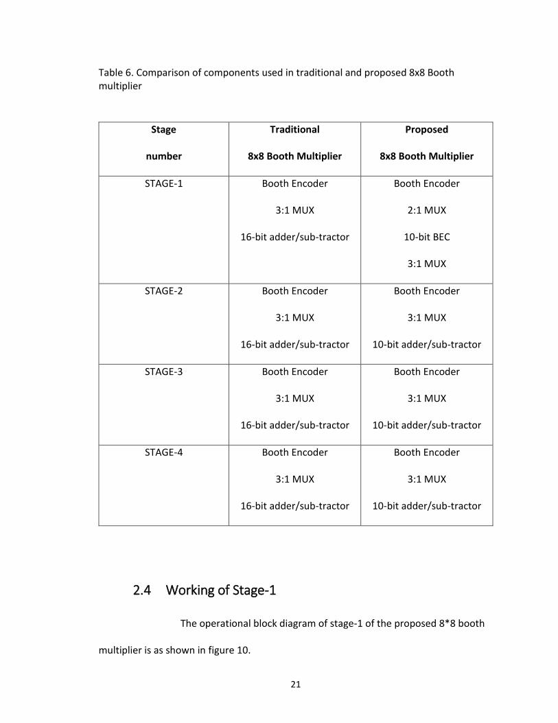
Table 6. Comparison of components used in traditional and proposed 8x8 Booth multiplier ..... 21
Table 7. Component comparison in two different styles of SQRT CSA.......................................... 34
Table 8. Comparison of result between 10-bit modified BEC and 10-bit SQRT CSA ..................... 44
Table 9. Metric comparison of components .................................................................................. 52
Table 10. Comparison of proposed booth multiplier with other multipliers ................................ 53
vi
LIST OF FIGURES
Figure 1 Block diagram of telecommunication field showing position of DMF ............................... 2
Figure 2. Grouping of multiplier bits in Radix-4 Booth algorithm.................................................... 7
Figure 3. Gate level implementation of Radix-4 Booth encoder ..................................................... 9
Figure 4. Gate level implementation of 1-bit full adder ................................................................ 10
Figure 5. Block diagram of 1-bit adder/sub-tractor ....................................................................... 12
Figure 6. 2^n-to-n Multiplexer ....................................................................................................... 13
Figure 7. Gate level implementation of 2:1 MUX .......................................................................... 14
Figure 8. Block diagram of traditional radix-4 8*8 booth multiplier ............................................. 18
Figure 9. Block diagram of the proposed radix-4 8*8 booth multiplier ........................................ 19
Figure 10. Block level implementation of stage-1. ........................................................................ 22
Figure 11. Gate level implementation of 10-bit regular BEC ......................................................... 24
Figure 12. Gate level implementation of 10-bit modified BEC ...................................................... 24
Figure 13. Gate level implementation of 3:1 MUX ........................................................................ 25
Figure 14. 10-bit MUX_3:1 ............................................................................................................. 26
Figure 15. Block diagram of stage-2/3/4 ....................................................................................... 28
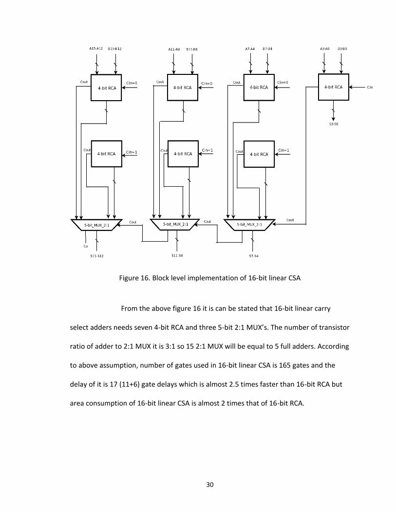
Figure 16. Block level implementation of 16-bit linear CSA .......................................................... 30
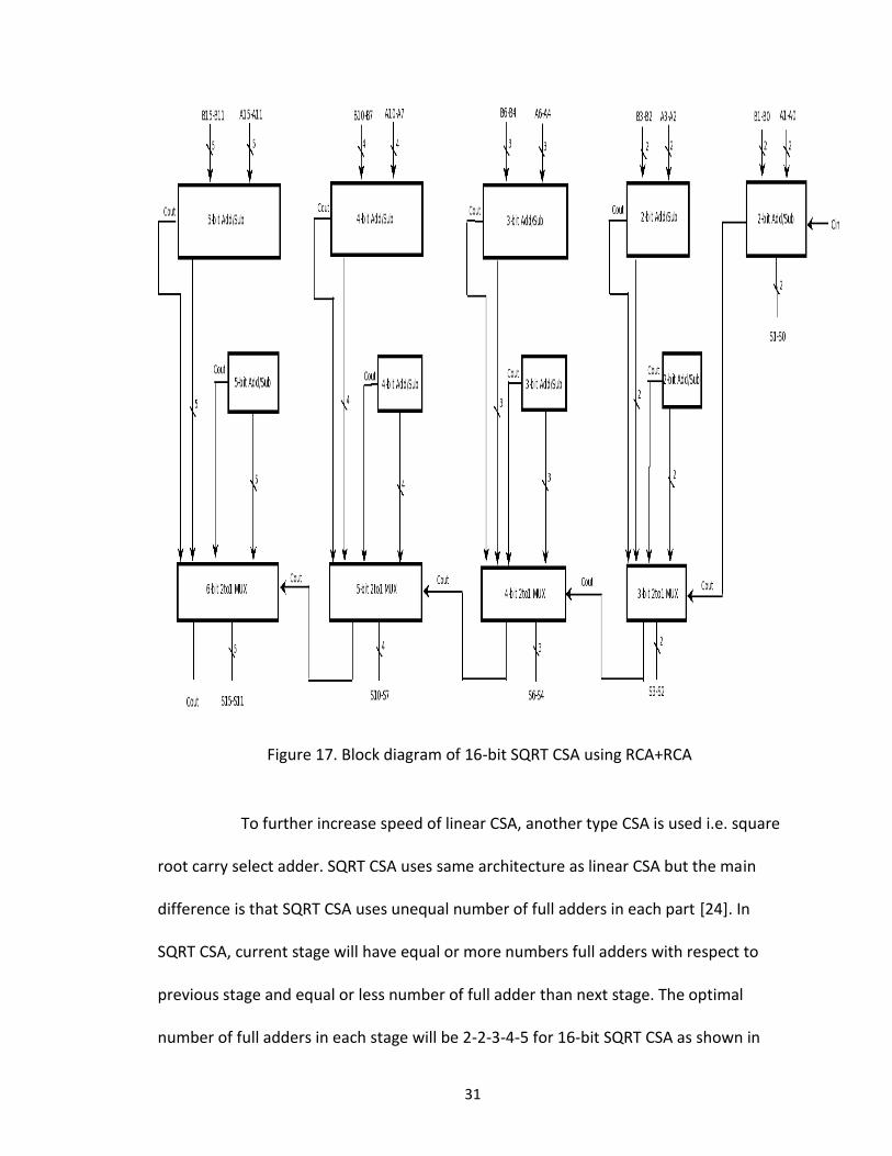
Figure 17. Block diagram of 16-bit SQRT CSA using RCA+RCA ....................................................... 31
Figure 18. Block diagram of 16-bit SQRT CSA using RCA+BEC ....................................................... 33
Figure 19. Block diagram of 10-bit SQRT CSA using RCA+RCA ....................................................... 34
Figure 20. Block diagram of 10-bit SQRT CSA using RCA+BEC ....................................................... 35
Figure 21. Block diagram of proposed 8x8 Booth multiplier ......................................................... 36

vii
Figure 22. PTL implementation of MUX 2:1 ................................................................................... 38
Figure 23. Simulation result of MUX 2:1 ........................................................................................ 39
Figure 24. PTL implementation of MUX 3:1 ................................................................................... 40
Figure 25. Simulation result of MUX 3:1 ........................................................................................ 41
Figure 26. PTL implementation of 1-bit Full Adder ........................................................................ 42
Figure 27. Simulation result of 1-bit Full Adder ............................................................................. 42
Figure 28. Simulation results of 10-bit modified BEC with inverters at input ............................... 45
Figure 29. Simulation results of radix-4 booth encoder ................................................................ 46
Figure 30. Simulation results and delay calculation of 10-bit SQRT CSA using RCA+RCA ............. 47
Figure 31. Simulation results and WPD calculation for proposed 8*8 booth multiplier ............... 49
Figure 32. Simulation results and BPD calculation for proposed 8*8 booth multiplier ................ 51

viii
ACKNOWLEDGEMENT
I would like to sincerely thank my advisor Dr. Saiyu Ren for her continuous guidance and
excellent advice. I wish to submit to her my wholehearted gratitude for all the support
and help I received from her. I would like to thank my thesis committee members Dr.
Ray Siferd and Dr. Jiafeng Xie. Finally, I would like to express my gratitude to my family
for their love and encouragement in all my endeavors throughout my academic career.
Rishit Patel, MSEE 2017

1
1. Introduction
1.1 Digital Matched Filter (DMF)
The application of digital matched filters are in the field of
communication such as code division multiple access (CDMA) and direct sequence
spread spectrum (DSSS), radar technology, global position system (GPS), image
processing, etc. [1] [2] [3] [4]. In signal processing, a matched filter is obtained by
correlating a known signal (i.e. transmitted signal), or template, with an unknown signal
to detect the presence of template in the unknown signal (i.e. received signal) [5] [6].
There are two basic types of matched filters available depending upon the area of
application such as analog matched filters (AMF) and digital matched filters (DMF). Both
the types of matched filters are used in the receiver part of the communication
discipline. Analog matched filters are usually used before analog-to-digital converter
(ADC) and digital matched filters are used after ADC which produces digital signal. The
block diagram depicting the place of digital matched filters in the field of
communication is shown in figure 1 [7].
The matched filter is the optimal linear filter for maximizing the signal to
noise ratio (SNR) in the presence of additive stochastic noise. Matched filtering is a
demodulation technique with LTI (linear time invariant) filters to maximize SNR. The
filter input, x (t) consists of a pulse signal g (t) corrupted by additive channel noise w (t),
as shown in below equation 1

2
𝑥(𝑡) = 𝑔(𝑡) + 𝑤(𝑡), 0 ≤ 𝑡 ≤ 𝑇 (1)
where T is an arbitrary observation interval. The pulse signal g (t) may represent a binary
0 or 1 in a digital communication system. Since the filter is linear, the resulting output y
(t) is expressed as shown in below equation (2):
𝑦(𝑡) = 𝑔(𝑡) + 𝑛(𝑡) (2)
Where g(t) and n(t) are produced by the signal and noise components of the input x(t),
respectively.
Figure 1 Block diagram of telecommunication field showing position of DMF
3
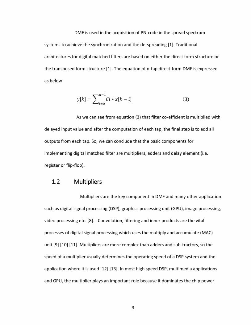
DMF is used in the acquisition of PN-code in the spread spectrum
systems to achieve the synchronization and the de-spreading [1]. Traditional
architectures for digital matched filters are based on either the direct form structure or
the transposed form structure [1]. The equation of n-tap direct-form DMF is expressed
as below
𝑦[𝑘] = ∑ 𝐶𝑖 ∗ 𝑥[𝑘 − 𝑖]𝑛−1
𝑖=0 (3)
As we can see from equation (3) that filter co-efficient is multiplied with
delayed input value and after the computation of each tap, the final step is to add all
outputs from each tap. So, we can conclude that the basic components for
implementing digital matched filter are multipliers, adders and delay element (i.e.
register or flip-flop).
1.2 Multipliers
Multipliers are the key component in DMF and many other application
such as digital signal processing (DSP), graphics processing unit (GPU), image processing,
video processing etc. [8]. . Convolution, filtering and inner products are the vital
processes of digital signal processing which uses the multiply and accumulate (MAC)
unit [9] [10] [11]. Multipliers are more complex than adders and sub-tractors, so the
speed of a multiplier usually determines the operating speed of a DSP system and the
application where it is used [12] [13]. In most high speed DSP, multimedia applications
and GPU, the multiplier plays an important role because it dominates the chip power

4
consumption and operation speed. So, research has concentrated on high-speed and
low-power multipliers for computationally fast portable devices. Any kind of multiplier is
divided into three stages such as partial product generation, partial products addition,
final-addition stage [12].
The speed of multiplication can be increased by reducing the number
partial products. Many high-performance algorithms and architectures have been
proposed to accelerate multiplication speed and keeping low power consumption in
mind. Various multiplication algorithms such as Booth, Braun, Wallace, Baugh-Woolley,
modified booth have proposed but each has its own importance and based upon that
they have specific applications [14].
1.2.1 Array Multiplier
The simplest form of multiplier is array multiplier [15]. It uses bunch
of half adders (HA), full adder (FA) and AND gates depending upon the multiplicand and
multiplier bits. The simplest way to perform multiplication is to use single two input
adders. Each bit of multiplier is AND-ed with multiplicand bit to produce partial products
and each time partial products are left shifted. The main drawback of array multiplier is
that it has large latency as it takes more clock cycles to compute the output [15]. The
number of partial products to be added is determined by the number of bits that the
multiplicand and multiplier have used. In order to get fast performance, one of the
methods is to arrange the circuit to generate all the partial products in parallel and
organize in an array.
5
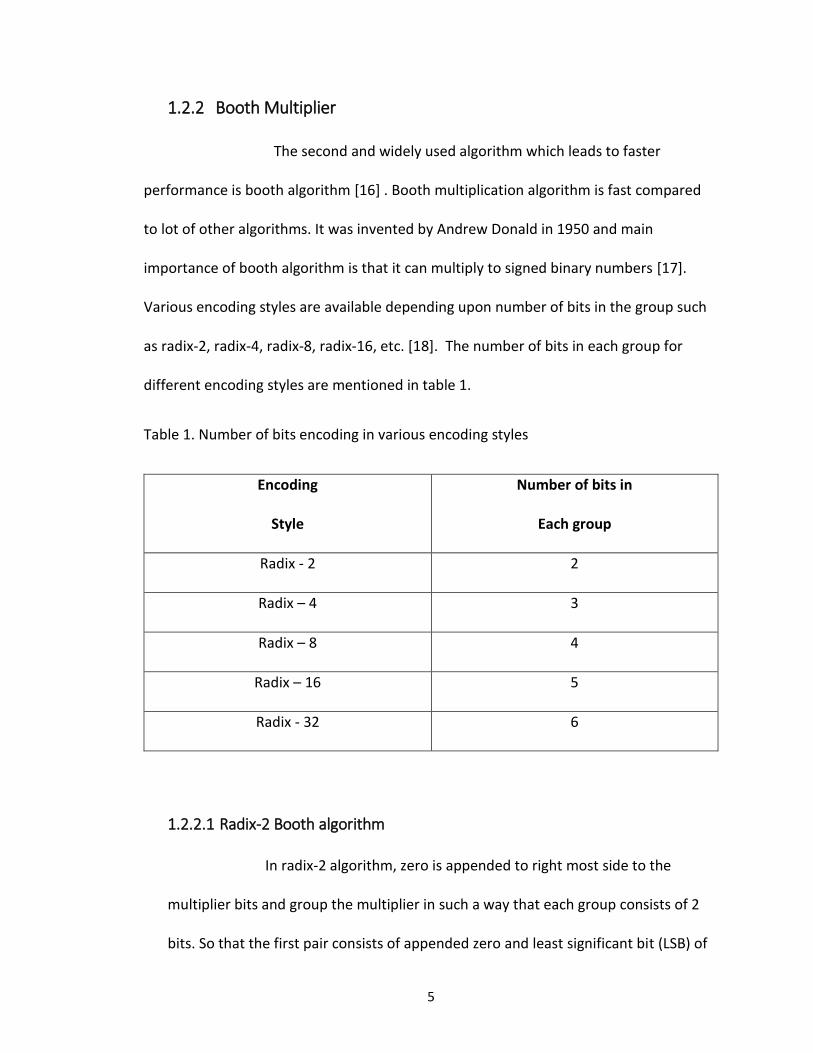
1.2.2 Booth Multiplier
The second and widely used algorithm which leads to faster
performance is booth algorithm [16] . Booth multiplication algorithm is fast compared
to lot of other algorithms. It was invented by Andrew Donald in 1950 and main
importance of booth algorithm is that it can multiply to signed binary numbers [17].
Various encoding styles are available depending upon number of bits in the group such
as radix-2, radix-4, radix-8, radix-16, etc. [18]. The number of bits in each group for
different encoding styles are mentioned in table 1.
Table 1. Number of bits encoding in various encoding styles
Encoding
Style
Number of bits in
Each group
Radix - 2 2
Radix – 4 3
Radix – 8 4
Radix – 16 5
Radix - 32 6
1.2.2.1 Radix-2 Booth algorithm
In radix-2 algorithm, zero is appended to right most side to the
multiplier bits and group the multiplier in such a way that each group consists of 2
bits. So that the first pair consists of appended zero and least significant bit (LSB) of

6
multiplier and the next pair is the overlapping of the first pair in which most
significant bit (MSB) of the first pair will be the LSB of the second pair. So that for n-
bit * n-bit multiplication, n partial products are obtained. Radix-2 booth algorithm
produces same number of partial products as array multiplier so number of cycles to
compute the result is almost similar.
1.2.2.2 Radix-4 Booth algorithm
To further decrease the number of partial products, algorithms
with higher radix value are used [18]. In radix-4 algorithm grouping of multiplier bits is
done in such a way that each group consists of 3 bits as mentioned in table 1. Similarly
the next pair is the overlapping of the first pair in which MSB of the first pair will be the
LSB of the second pair and other two bits. Number of groups formed is dependent on
number of multiplier bits. By applying this algorithm, the number of partial product
rows to be accumulated is reduced from n in radix-2 algorithm to n/2 in radix-4
algorithm [19]. The grouping of multiplier bits for 8-bit of multiplication is shown in
figure 2.

7
Figure 2. Grouping of multiplier bits in Radix-4 Booth algorithm
For 8-bit multiplier the number groups formed is four using radix-4
booth algorithm. Compared to radix-2 booth algorithm the number of partial
products obtained in radix-4 booth algorithm is half because for 8-bit multiplier
radix-2 algorithm produces eight partial products. The truth table and the respective
operation is depicted in table 2. Similarly when radix-8 booth algorithm is applied to
multiplier of 8-bits each group will consists of four bits and the number of groups
formed is 3. For 8x8 multiplication, radix-4 uses four stages to compute the final
product and radix-8 booth algorithm uses three stages to compute the product. In
this thesis, radix-4 booth algorithm is used for 8x8 multiplication because number
components used in radix-4 encoding style is much less compared radix-8 encoding
style as discussed in table 3 which decreases consumption and delay as well.

8
Table 2. Truth Table for Radix-4 Booth algorithm
Table 3. Comparison of components between radix-4 and radix-8 encoding style
Radix-4 encoding Radix-8 encoding
Stages 4 3
Booth encoder 3-bit 4-bit
Multiplexers 3:1 MUX 5:1 MUX
1-bit adder/sub-tractor 64(16 in each stage) 72 (24 in each stage)
The multiplier bits are provided to booth encoder which produces 3-bit output which
will perform operations like 0, ±A or ±2A depending upon inputs. Operations can be
performed with the help of multiplexer (MUX) and adder/sub-tractor blocks. For
Bi+1 Bi Bi-1 Operation Yi+1 Yi Yi-1
0 0 0 +0 0 0 0
0 0 1 +A 0 1 0
0 1 0 +A 0 1 0
0 1 1 +2A 0 0 1
1 0 0 -2A 1 0 1
1 0 1 -A 1 1 0
1 1 0 -A 1 1 0
1 1 1 -0 1 0 0

9
example, as shown in table 2, if 100 bit is provided to booth encoder, then it will
produce 101 output. The output of this MSB (Yi+1) is used to select adder or sub-tractor
and two LSB (Yi and Yi-1) is used to select 2A from multiplexer. From the above
discussion it is clear that the essential components for implementing radix-4 booth
algorithm are booth encoder, adder/sub-tractor and multiplexer (MUX). The gate level
implementation of radix-4 booth encoder is shown in figure 3.
Figure 3. Gate level implementation of Radix-4 Booth encoder
1.3 Adder/Sub-tractor
The main function of adder block is to add two binary numbers. Half
adder adds two bits at a time while, full adder adds three bits at same instance. Full
adder can be implemented using two half adders as shown in figure 4. The inputs to full

10
adder are A, B and carry-in (Cin) and the outputs are sum (S) and carry-out (Co). The
Boolean equation for sum (S) and carry-out (Co) are as follows:
𝑆 = 𝐴 𝑥𝑜𝑟 𝐵 𝑥𝑜𝑟 𝐶𝑖𝑛 (4)
𝐶𝑜 = ((𝐴 𝑥𝑜𝑟 𝐵) 𝑛𝑎𝑛𝑑 𝐶𝑖𝑛) 𝑛𝑎𝑛𝑑 (𝐴 𝑛𝑎𝑛𝑑 𝐵) (5)
Truth table of 1-bit full adder is as shown in table 4. It uses 8
different combinations of input and based upon that it produces outputs related to sum
and carry bit.
Figure 4. Gate level implementation of 1-bit full adder

11
Table 4. Truth Table for 1-bit full adder
A B Cin S Cout
0 0 0 0 0
0 0 1 1 0
0 1 0 1 0
0 1 1 0 1
1 0 0 1 0
1 0 1 0 1
1 1 0 0 1
1 1 1 1 1
. In many computer and other kinds of processors, adders are used not
only in the arithmetic logic unit (ALU), but also in other parts of the processor, where
they are used to calculate addresses, table indices, increment and decrement
operations, and similar operations.
In cases where two’s complement and one’s complement is being used
to represent negative numbers, it is very important to convert adder into adder-sub-
tractor block. Adder block can be converted to adder-sub-tractor block using carry-in
(Cin) as control line such that if Cin = 0 the block will perform addition and if Cin = 1 the
block will perform subtraction. An additional gate i.e. XOR is added to the block to

12
perform addition and subtraction using single block. The implementation of adder sub-
tractor block is as shown in figure 5.
Figure 5. Block diagram of 1-bit adder/sub-tractor
1.4 Multiplexer
In VLSI, the multiplexer is a device that selects one of several analog or
digital input signals and forwards the selected input into a single line. A multiplexer of
2n inputs has n select lines, which are used to select which input line to send to the
output as shown in the figure 6.

13
Figure 6. 2^n-to-n Multiplexer
Depending upon the inputs to select lines, specific input is selected and
provided to output. Booth multiplier uses 2:1 MUX and 3:1 MUX of various bit length.
The simplest multiplexer is 2:1 MUX which has two inputs, one select line and one
output is selected. For example, A and B are the two inputs, S is the select line and Z is
the output for 2:1 MUX then Boolean equation of 2:1 MUX is as shown below:
𝑍 = 𝐴 · 𝑆′ + 𝐵 · 𝑆 (6)
The truth table of 2:1 MUX is listed in table 4 and gate level
implementation of 2:1 MUX is as shown in figure 7.
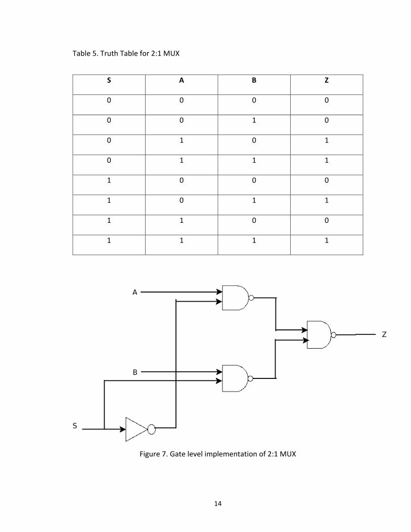
14
Table 5. Truth Table for 2:1 MUX
S A B Z
0 0 0 0
0 0 1 0
0 1 0 1
0 1 1 1
1 0 0 0
1 0 1 1
1 1 0 0
1 1 1 1
Figure 7. Gate level implementation of 2:1 MUX
15
1.5 Objective & Motivation
1.5.1 Objective
The objective of this thesis is to design high-speed and low-power
multiplier for digital matched filters. Booth multiplication algorithm is used in this thesis
to implement high speed and low power multiplier for digital matched filters.
Multipliers use adders to add the partial products generated at each stages to compute
the final product. So the need of high speed and low power adders are the basic
necessary to implement booth multipliers.
1.5.2 Motivation
With the increasing requirement for huge number of functionalities
performed by a single chip, semiconductor industries are trying to encompass billions of
transistors in a small space. Speed of the operations is in the great need while reducing
the power consumption. The goal for every designer is to design a low power, high
speed and low cost chips. Some applications require more speed while others require
less power consumption and lower area to build more functionalities on the chip. But
we cannot achieve all the parameters at the same time because there is always a trade-
off between this components [20]. For example, the ripple carry adder is simple to
design but the computation speed is very low. Some parallel prefix adders like kogge-
stone adder, Brent-kung adder, etc. provides fast output but consumes high area as well
as high power. Performance specifications in digital designs can be achieved by scaling
the transistor sizes. Technology is scaling to atomic sizes. Technology scaling along with

16
novel and efficient techniques for implementation of digital design helps reducing the
size and power consumption while keeping the speed of operation almost same.
There are many research undertaken for implementation of high-speed
and low-power multipliers. Growing demands for portable, battery-powered systems
necessitates low power matched filters to reduce the power consumption of code
acquisition circuits. Low-power matched filters can be implemented by using either
analog or digital technology. For short and fast matched filters, analog implementation
is more power efficient than digital counterpart [21]. As complementary metal-oxide
semiconductor (CMOS) technology advances rapidly and the reference code length in
modern wireless communication systems increases, significant attention has focused on
high-speed and low-power DMF’s. For high-speed and low-power DMF’s, we need
multipliers with high-speed and low-power consumption.
1.6 Thesis Organization
The rest of the thesis is organized as follows: Chapter 2 discusses the
proposed booth multiplier using CMOS technology to design high-speed and low-power
8x8 booth multiplier. The implementation of the proposed 8x8 booth multiplier is
custom-designed in SAED32nm technology and simulated using wave-viewer provided
by Synopsys, which are detailed in Chapter 3. Finally, conclusion and future work are
included in Chapter 4.

17
2 Proposed Radix-4 8x8 Booth Multiplier
The proposed radix-4 8x8 booth multiplier uses same architecture as
traditional booth multiplier but eliminates the circuit which is not used for computation.
For 8x8 multiplication, both traditional and proposed booth multiplier uses four stages
to compute the final product. Traditional 8x8 booth multiplier uses same type of
component in all the four stages shown in figure 8. In each stage it uses components like
booth encoder, 16-bit adder/sub-tractor block and 16-bit 3:1 MUX. The multiplier bits
with appended is zero is applied to booth encoder of each block. The input to booth
encoder of stage-1, stage-2, stage-3 and stage-4 are B1-B0-0, B3-B2-B1, B5-B4-B3 and
B7-B6-B5 respectively and generate output depending upon inputs. The operation of all
the four stages is similar. The MSB of the output of booth encoder is applied to
adder/sub-tractor block which will select adder if input to block is 0 and select sub-
tractor if input to block is 1. The two LSB of the output of booth encoder is applied to
multiplexer block which will select either 0, ‘A’ or ‘2A’ depending upon the structure of
3:1 MUX. If the input to multiplexer block is 00 it will select 0 input, if 01 it will select ‘A’
and if 10 it will select ‘2A’ as an output.
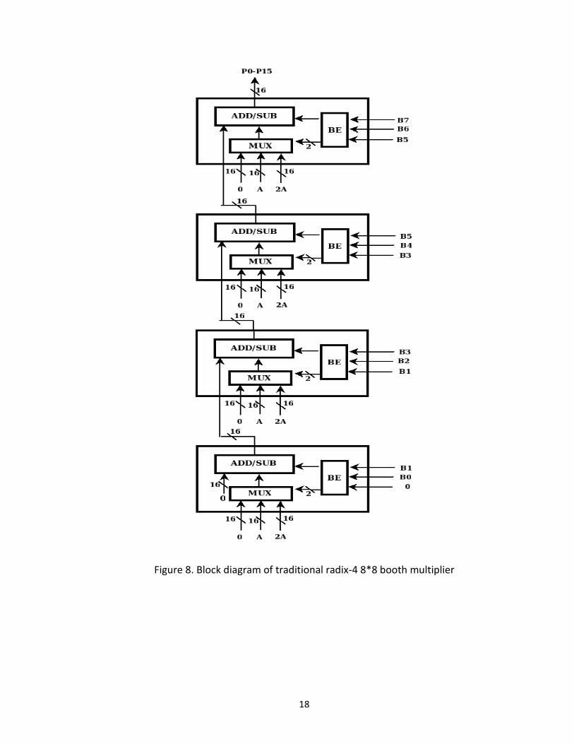
18
Figure 8. Block diagram of traditional radix-4 8*8 booth multiplier

19
Figure 9. Block diagram of the proposed radix-4 8*8 booth multiplier
After selection of selection of which input to select i.e. 0, ‘A’ or ‘2A’, the
output of MUX is provided to the adder/sub-tractor block. The other input to
adder/sub-tractor block is the output from previous block. For the 1st stage, the inputs

20
to adder/sub-tractor block are zero and output from multiplexer. The proposed radix-4
8*8 booth multiplier uses 10-bit adder/sub-tractor in stage-2, stage-3 and stage-4 while
in stage-1 it uses 10-bit modified BEC instead of adder/sub-tractor block to reduce the
power consumption and latency. The block diagram for the proposed radix-4 8*8 booth
multiplier is shown in figure 9. The comparison of components used in traditional and
proposed booth multiplier is listed as shown in table 5. As seen in the table 6 that
traditional 8x8 booth multiplier uses booth encoder, 16-bit adder/sub-tractor block and
16-bit 3:1 MUX in all the four stages. The proposed radix-4 8*8 booth multiplier uses
booth encoder, 10-bit adder/sub-tractor and 10-bit 3:1 MUX in stage-2, stage-3 and
stage-4 while stage-1 uses booth encoder, 10-bit 3:1 MUX, 10-bit modified BEC and 10-
bit 2:1 MUX. The proposed 8x8 Booth multiplier uses different set of components in all
stages as compared to traditional 8x8 Booth multiplier. The proposed 8x8 Booth
multiplier uses booth encoder, 10-bit 3:1 MUX, 10-bit modified binary-to-excess-1
converter BEC and 10-bit 2:1 MUX in stage-1. Stage-2/3/4 of proposed 8x8 Booth
multiplier is implemented using booth encoder, 10-bit adder/sub-tractor block and 10-
bit 3:1 MUX. So in total proposed design uses four booth encoder, four 10-bit 3:1 MUX,
one 10-bit 2:1 MUX, one 10-bit modified BEC and three 10-bit adder/sub-tractor. From
table 5 we can conclude that we saved area by using less bit length of components,
which in turn saves power consumption. The operation of each stage is explained in this
section.
21
Table 6. Comparison of components used in traditional and proposed 8x8 Booth multiplier
Stage
number
Traditional
8x8 Booth Multiplier
Proposed
8x8 Booth Multiplier
STAGE-1 Booth Encoder
3:1 MUX
16-bit adder/sub-tractor
Booth Encoder
2:1 MUX
10-bit BEC
3:1 MUX
STAGE-2 Booth Encoder
3:1 MUX
16-bit adder/sub-tractor
Booth Encoder
3:1 MUX
10-bit adder/sub-tractor
STAGE-3 Booth Encoder
3:1 MUX
16-bit adder/sub-tractor
Booth Encoder
3:1 MUX
10-bit adder/sub-tractor
STAGE-4 Booth Encoder
3:1 MUX
16-bit adder/sub-tractor
Booth Encoder
3:1 MUX
10-bit adder/sub-tractor
2.4 Working of Stage-1
The operational block diagram of stage-1 of the proposed 8*8 booth
multiplier is as shown in figure 10.

22
Figure 10. Block level implementation of stage-1.
As shown in figure 10, the inputs to 10-bit 3:1 MUX of stage-1 are 8-bit
zero, 8-bit of multiplicand A and 9-bit of 2A. The inputs to booth encoder of stage-1 are
appended zero and two LSB of multiplier bit. Depending on the output of booth
encoder, stage-1 decides to get 0, A or 2A from 10-bit 3:1 MUX and whether to select
output from 10-bit 3:1 MUX or 10-bit modified BEC. The input to 10-bit modified BEC is
inverted output from 10-bit 3:1 MUX. The input to 10-bit 2:1 MUX is output from 10-bit
modified BEC and output from 10-bit 3:1 MUX. As one input to stage-1 is all zero so

23
adder/sub-tractor block is replaced by 10-bit modified BEC and 10-bit 2:1 MUX. So the
output of stage-1 will be either output from 10-bit modified BEC or from 10-bit 3:1
MUX.
2.4.1 10-bit Modified BEC
The function of binary-to-excess-1 converter is to add 1 to whatever the
input is provided. The main advantage to using BEC is in carry select adder (CSA) to
reduce the number of gates so we can decrease area consumption and by doing so
power consumption can also be reduced. For example, 4-bit BEC has four inputs and 5-
bit output if it has carry. The Boolean equation for 4-bit of BEC is written below:
𝑋0 = 𝐵0′
𝑋1 = 𝐵1 𝑥𝑜𝑟 𝐵0
𝑋2 = (𝐵1 𝑎𝑛𝑑 𝐵0) 𝑥𝑜𝑟 𝐵2
𝑋3 = (𝐵2 𝑎𝑛𝑑 𝐵1 𝑎𝑛𝑑 𝐵0) 𝑥𝑜𝑟 𝐵3
Where B0, B1, B2 and B3 are the input to 4-bit BEC and X0, X1, X2 and X3 are
respectively the output of 4-bit BEC.
The gate level implementation of regular 10-bit BEC is as shown in
figure 11. As it can be seen from figure 11 that each AND_2 gate have to wait for
previous AND_2 gate. The inputs to each AND_2 are present input (Bi) and output from
previous AND_2 gate. So the total delay of 10-bit regular BEC is as shown in equation
below:

24
𝑇𝑑 = 8 ∗ (𝐷𝑒𝑙𝑎𝑦 𝑜𝑓 𝐴𝑁𝐷2) + 𝐷𝑒𝑙𝑎𝑦 𝑜𝑓 𝑋𝑂𝑅2
Figure 11. Gate level implementation of 10-bit regular BEC
The delay of regular 10-bit BEC can be reduced by replacing all AND_2
gates with repeating structure of AND_2, AND_3 and AND_4 i.e. 2-3-4 from left to right.
The gate level implementation of 10-bit modified BEC is as shown in figure 12.
Figure 12. Gate level implementation of 10-bit modified BEC

25
As shown in the figure 12, structure 2-3-4 is used to implement 10-bit
modified BEC. Here every time present AND gate have not to wait for previous AND
gate. The changes made are instead of using 8 AND_2 it uses 3 AND_2, 3 AND_2 and 2
AND_4. The input to AND_4 gate will be present input (Bi) and three previous inputs.
The output of AND_4 is applied to AND_2 and AND_3 to its left as shown in figure 12. So
the delay of 10-bit modified BEC will be given by equation below:
𝑇𝑑 = 2 ∗ (𝐷𝑒𝑙𝑎𝑦 𝑜𝑓 𝐴𝑁𝐷4) + 𝐷𝑒𝑙𝑎𝑦 𝑜𝑓 𝐴𝑁𝐷3 + 𝐷𝑒𝑙𝑎𝑦 𝑜𝑓 𝑋𝑂𝑅2
2.4.2 10-bit 3:1 MUX
The purpose of using 3:1 MUX is to select either 0, A or 2A. The select
lines for 3:1 MUX are two, which is provided from the output from booth encoder. We
are using 10-bit 3:1 MUX because as we are giving 8-bit multiplicand, so if we left shift it
we will get 9-bits for 2A and the output provided to 2:1 MUX and modified BEC is also
10-bit. Gate level implementation of 3:1 MUX for function 7 by using three NAND_3
gates and two inverters are shown in figure 13.
Figure 13. Gate level implementation of 3:1 MUX

26
𝑍 = (𝐴 𝑛𝑎𝑛𝑑 𝑆0′𝑛𝑎𝑛𝑑 𝑆1′) 𝑛𝑎𝑛𝑑 (𝐵 𝑛𝑎𝑛𝑑 𝑆0′𝑛𝑎𝑛𝑑 𝑆1) 𝑛𝑎𝑛𝑑 (𝐶 𝑛𝑎𝑛𝑑 𝑆0 𝑛𝑎𝑛𝑑 𝑆1′) (7)
To implement 10-bit 3:1 MUX, ten 1-bit 3:1 MUX are connected in parallel to
produce 10-bit of output as shown in figure 14. The 8-bit zeros (i.e. 00000000) is applied
to top input of 3:1 MUX, 8-bit multiplicand is applied to middle input of 3:1 MUX and
left shifted multiplicand is provided to bottom input of 3:1 MUX. For two remaining 3:1
MUX in 10-bit 3:1 MUX two top inputs will be 00 and two middle inputs will be MSB of
multiplicand. And for the 10th 3:1 MUX the bottom input will be the MSB of multiplicand
left shifted by 1. 10-bit 3:1 MUX produces 10-bit output which is provided to modified
BEC and 10-bit 2:1 MUX.
Figure 14. 10-bit MUX_3:1

27
2.4.3 10-bit 2:1 MUX
The purpose of 10-bit 2:1 MUX in stage-1 is to select either 10-bit output
from modified BEC or 10-bit output from 3:1 MUX. 10-bit 2:1 MUX uses MSB of booth
encoder as its select line to choose from two inputs. The gate level implementation of
2:1 MUX is as discussed above in figure 7. 10-bit 2:1 MUX is implemented using ten 2:1
MUX in parallel. The inputs to 10-bit 2:1 MUX are 10-bit output from 3:1 MUX and 10-bit
output from 10-bit modified BEC. 10-bit 2:1 MUX produces 10-bit output out of that two
LSB is provided to final product, that will become P0 and P1 bit of final product and the
remaining eight bits are provided to 10-bit adder/sub-tractor block of stage-2.
2.5 Working of Stage-2/3/4
As it is seen in figure 15, stage-2/3/4 are implemented using booth
encoder, 10-bit 3:1 MUX and 10-bit adder/sub-tractor block. The input to booth encoder
of stage-2, stage-3 and stage-4 are B3-B2-B1, B5-B4-B3 and B7-B6-B5 respectively. The
function of stage-2, stage-3 and stage-4 are same, just the inputs to each stage changes,
so working of stage-2 is discussed first and then overview of the functioning of stage-3
and stage-4 are discussed. The input to 3:1 MUX of traditional 8x8 booth multiplier of
stage-2 is the multiplicand bits left shifted by 2 but in the proposed 8x8 booth
multiplier, input to 10-bit 3:1 MUX is the same multiplicand bits. There is no need to left
shift the multiplicand bits because of the architecture of proposed 8x8 Booth multiplier.
Traditional Booth multiplier uses circuitry for left shift by 2 in each stages but proposed

28
8x8 Booth multiplier do not need that circuitry because of its architecture. The output of
10-bit 3:1 MUX is provided to 10-bit adder/sub-tractor block as discussed earlier.
Figure 15. Block diagram of stage-2/3/4
2.5.1 10-bit Adder/Sub-tractor
As discussed earlier, the function of adder/sub-tractor circuitry is to add
or subtract two binary numbers depending upon the Cin. If Cin = 0, it will perform

29
addition else if Cin = 1 it will perform subtraction. Depending upon the requirement, we
can select which type of adders to use. For example, if the requirement is less area we
can select ripple carry adder (RCA) because the complexity of it is low, but the drawback
of it is that it has high delay. And if the requirement is high speed we can use parallel
prefix adders Kogge-Stone, Brent-Kung, etc. but they consume very high compared to ripple
carry adders. The optimal adder for high speed and minimal area consumption is carry select
adders (CSA).
Carry select adders are one of the fastest adders available in VLSI industry
and the operation of it is explained using 10-bit adder [22]. Usually there will be two
blocks of full adders in each part except first part such that first part will have one block
of n–bit full adders while remaining part will have two blocks of n-bit full adders [23].
The reason for using two blocks of full adders is that first block will compute sum and
carry-out by assuming carry-in Cin = 0 and second block will compute sum and carry-out
by assuming carry-in Cin = 1 in advance. As CSA adders compute sum and carry-out by
assuming to different situation such as Cin = 0 and Cin = 1 so carry-out from previous
block is used to select sum and carry-out for present block using multiplexer (MUX).
There are two main types of carry select adders such as linear carry
select adders known as CSA and square root carry select adders (SQRT CSA). The main
difference between these types of adders is that linear CSA uses equal number of bit
blocks while SQRT CSA uses unequal number of full adders in each block. The block level
implementation of 16-bit linear carry select adders is as shown in figure 16 and block
level implementation of 16-bit square root carry select adders is as shown in figure 17.
30
Figure 16. Block level implementation of 16-bit linear CSA
From the above figure 16 it is can be stated that 16-bit linear carry
select adders needs seven 4-bit RCA and three 5-bit 2:1 MUX’s. The number of transistor
ratio of adder to 2:1 MUX it is 3:1 so 15 2:1 MUX will be equal to 5 full adders. According
to above assumption, number of gates used in 16-bit linear CSA is 165 gates and the
delay of it is 17 (11+6) gate delays which is almost 2.5 times faster than 16-bit RCA but
area consumption of 16-bit linear CSA is almost 2 times that of 16-bit RCA.
31
Figure 17. Block diagram of 16-bit SQRT CSA using RCA+RCA
To further increase speed of linear CSA, another type CSA is used i.e. square
root carry select adder. SQRT CSA uses same architecture as linear CSA but the main
difference is that SQRT CSA uses unequal number of full adders in each part [24]. In
SQRT CSA, current stage will have equal or more numbers full adders with respect to
previous stage and equal or less number of full adder than next stage. The optimal
number of full adders in each stage will be 2-2-3-4-5 for 16-bit SQRT CSA as shown in

32
figure 17. Gate delay for 16-bit SQRT CSA is 13 out of which 2-bit FA have gate delay of 5
and four multiplexer will have delay of 8 but it increases area consumption as well as
power consumption compared to linear CSA. As per the requirement of high speed
booth multiplier it is implemented using square root carry select adder.
To further decrease area and power consumption of SQRT CSA, dual RCA in
each stage is replaced by one RCA and one BEC [25]. RCA will compute result for Cin=0
and output is applied to BEC and it will perform same operation as RCA with Cin=1 [26] .
The block diagram of 16-bit SQRT CSA using RCA+BEC combination is as shown in figure
18.
The delay equation for N-bit linear CSA with M stages is given by:
𝑇 = 𝑡(𝑠𝑒𝑡𝑢𝑝) + (𝑁
𝑀) ∗ 𝑡(𝑐𝑎𝑟𝑟𝑦) + 𝑀 ∗ 𝑡(𝑚𝑢𝑥) + 𝑡(𝑠𝑢𝑚)
The delay equation for N-bit SQRT CSA with P stages is given by:
𝑇 = 𝑡(𝑠𝑒𝑡𝑢𝑝) + 𝑃 ∗ 𝑡(𝑐𝑎𝑟𝑟𝑦) + (2𝑁)^0.5 ∗ 𝑡(𝑚𝑢𝑥) + 𝑡(𝑠𝑢𝑚)
From the above discussion we can conclude that square root carry select
adder using RCA+RCA provides you the higher speed compared to linear CSA and SQRT
using RCA+BEC.
So, square root carry select adder using RCA+RCA is used to implement 10-
bit SQRT CSA because it gives high speed compared to other techniques of carry select
adders.

33
Figure 18. Block diagram of 16-bit SQRT CSA using RCA+BEC
2.5.1.1 10-bit SQRT CSA using RCA+RCA
The block diagram of 10-bit SQRT CSA using RCA+RCA is shown in figure 19.
The summary and comparison of components used in 10-bit SQRT CSA using RCA+RCA
and 10-bit SQRT CSA using RCA+BEC are shown in table 6.

34
Figure 19. Block diagram of 10-bit SQRT CSA using RCA+RCA
Table 7. Component comparison in two different styles of SQRT CSA
10-bit SQRT CSA
Using RCA+RCA
10-bit SQRT CSA
Using RCA+BEC
1-bit full adder 19 10
BEC - 4
Multiplexer 4 4
Delay (ps) 147 193

35
2.5.1.2 10-bit SQRT CSA using RCA+BEC
The block diagram of 10-bit SQRT CSA using RCA+BEC is shown in figure
20.
Figure 20. Block diagram of 10-bit SQRT CSA using RCA+BEC
The inputs to 10-bit SQRT CSA using RCA+RCA are output from 10-bit 3:1
MUX from stage-2 and output from stage-1. It will perform addition or subtraction
depending upon select line and produces 11-bit of output, of which MSB is the carry-
out. From the remaining 10-bit, two LSB are directly sent to final output and they are P2

36
and P3 bits of final product, and eight bits are sent to adder/sub-tractor block of stage-
3.
Similarly, stage-3 produces 11-bits, of which MSB is the carry-out and two
LSB are directly sent to final output and they are P4 and P5 bits of final product and
remaining eight bits are provided to adder/sub-tractor block of stage-4. The output of
stage-4 will become P15-P6 bits of final product. So the final product is made up of 16-
bits i.e. P15-P0.
Figure 21. Block diagram of proposed 8x8 Booth multiplier
37
3 Implementation of proposed 8*8 Booth Multiplier in
32nm CMOS Technology
From the discussion in Chapter 2, it can be concluded that the main sub-
components used in the implementation of proposed 8*8 booth multiplier are MUX 2:1,
MUX 3:1 and 1-bit full adder. The above listed sub-components are used to implement
higher level blocks like 10-bit MUX 2:1, 10-bit MUX 3:1 and 10-bit SQRT CSA using
RCA+RCA respectively. The basic gates used in the implementation of booth encoder
and 10-bit modified BEC with inverter are 2-input XOR, 2, 3, 4-input AND gate and
inverter. MUX 2:1, MUX 3:1 and 1-bit full adder are implemented using pass transistor
logic (PTL) while inverter, 2-input XOR gate and 2, 3, 4- input gate are implemented
using static logic. All components are implemented in 32nm complementary metal oxide
semiconductor (CMOS) technology. The main purpose of using PTL is to decrease area
and delay in basic element so that overall area of the design is decreased and speed is
increased. Static inverters are added at the output of PTL logic to boost the weak
outputs caused by the pass transistor to be strong logic. By doing so we can overcome
the disadvantage of PTL and keeping area low and faster. Pass transistor logic often uses
fewer transistors, runs faster and requires less power than the same function
implemented with the same transistors in fully complementary CMOS logic [27]. As the
technology is scaling down, power supply of design is also decreasing with scaling
technology. As integrated circuit supply voltages decreases, the disadvantages of pass
transistor logic become more significant; the threshold voltage of transistors becomes
large compared to supply voltage, severely limiting the number of sequential PTL stages.

38
3.1 Implementation of sub-components in 32nm CMOS technology
Schematic implementation in 32nm of MUX 2:1, MUX 3:1 and 1-bit full adder is
explained here with their results (i.e. waveforms) showing delay and power
consumption.
3.1.1 MUX 2:1
Schematic view of MUX 2:1 using PTL is shown in figure 22. As seen in figure
22, 2 NMOS transistors and 3 inverters are used to implement MUX 2:1. The gate of one
NMOS transistor is connected to select line S and another with S’. Input A is connected
to drain terminal of one NMOS and input B is connected to drain terminal of another
NMOS transistor. Two inverters are connected at output to boost the output logic and
increase the drive strength of MUX 2:1. Compared to CMOS logic, PTL saves 33% area
based on the number of transistors.
Figure 22. PTL implementation of MUX 2:1

39
Simulation result of MUX 2:1 using PTL logic is shown in figure 23. The
propagation delay tHL and tLH are 15.2 ps and 24 ps respectively and the power
consumption is 0.567 uW at 1 GHz input frequency.
Figure 23. Simulation result of MUX 2:1
3.1.2 MUX 3:1
Schematic view of MUX 3:1 using PTL is shown in figure 24. As seen in
figure, 6 NMOS transistors and 4 inverters are used to implement MUX 3:1. There are
three pair of two NMOS transistors and gate of first pair is connected to S0’ and S1’
respectively. Similarly, gate of other two pairs are S0’ and S1, S0 and S1’ respectively.
Input A is connected to drain terminal of first NMOS transistor in first pair. Similarly,
inputs B and C are connected to drain terminal of second and third pair respectively. The

40
source terminal of all three pairs are connected to two inverters to increase the drive
strength of MUX 3:1.
Simulation result of MUX 3:1 using PTL logic is shown in figure 25. The
propagation delay tHL and tLH are 21.2 ps and 49.7 ps respectively and the power
consumption is 1.33 uW at 1 GHz input frequency. The number of transistors used in
MUX 3:1 with PTL is 14 which is less compared to static CMOS implementation with 28
transistors needed.
Figure 24. PTL implementation of MUX 3:1

41
Figure 25. Simulation result of MUX 3:1
3.1.3 1-bit Full Adder
The implementation of 1-bit full adder with PTL logic is shown in figure 26. Full
adder uses 12 NMOS transistors and five inverters. Out of five inverters, three inverters
are used to get inverted inputs and other two inverters are connected at outputs to
increase the drive strength of PTL logic. As shown in the figure 26, the upper part is used
to get the sum of full adder and lower part is used to get carry-out of 1-bit full adder.
The number of transistors used in 1-bit full adder with PTL is 22 which are less compared
to 1-bit mirror adder static CMOS implementation (i.e. 28 transistors).

42
Figure 26. PTL implementation of 1-bit Full Adder
Simulation result of 1-bit full adder using PTL logic is shown in figure 27. The
propagation delay tHL and tLH are 25.1 ps and 8.46 ps respectively and the power
consumption is 1.63 uW at 1 GHz input frequency.
Figure 27. Simulation result of 1-bit Full Adder

43
3.2 Results of Sub-components
This section includes the results of each sub-components of proposed 8*8
booth multiplier such as booth encoder, 10-bit modified binary-to-excess one converter
(BEC) with inverter, 10-bit SQRT CSA using RCA+RCA. The result of 10-bit MUX 3:1 and
10-bit MUX 2:1 is usually same as 1-bit MUX 3:1 and 1-bit MUX 2:1 instead we are using
10 components in parallel. The delay of 10-bit MUX’s will be same as 1-bit MUX because
computation is carried in parallel.
3.2.1 Result of 10-bit modified BEC with inverters at input
10-bit modified BEC with inverter at input is used in the stage-1 as discussed
in chapter 2, which removes the need of using 10-bit adder/sub-tractor. The
functionality of 10-bit modified BEC with inverters at input is same as that of 10-bit
adder in stage-1 because there is no second input coming from previous block. Using 10-
bit modified BEC with inverters at input in stage-1 and 10-bit MUX 2:1 instead of 10-bit
adder/sub-tractor decreases number of transistor counts and finally area consumption
is decreased. The schematic of 10-bit modified BEC with inverters at input is same as
shown in figure 12. As you can see from figure it is implemented using 2-3-4 AND
structure which helps in reduction of delay compared to regular 10-bit BEC. As seen
from the block diagram of stage-1 and stage-2/3/4, we see that stage-1 consist 10-bit
modified BEC with inverters at input and 10-bit MUX 2:1 instead of 10-bit SQRT CSA
using RCA+RCA. The comparison of result including delay, power and transistor count
between 10-bit BEC and 10-bit adder/sub-tractor is shown in table 7.
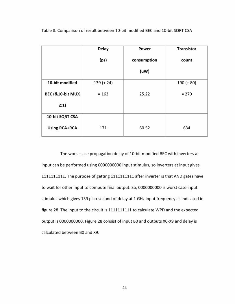
44
Table 8. Comparison of result between 10-bit modified BEC and 10-bit SQRT CSA
Delay
(ps)
Power
consumption
(uW)
Transistor
count
10-bit modified
BEC (&10-bit MUX
2:1)
139 (+ 24)
= 163
25.22
190 (+ 80)
= 270
10-bit SQRT CSA
Using RCA+RCA
171
60.52
634
The worst-case propagation delay of 10-bit modified BEC with inverters at
input can be performed using 0000000000 input stimulus, so inverters at input gives
1111111111. The purpose of getting 1111111111 after inverter is that AND gates have
to wait for other input to compute final output. So, 0000000000 is worst case input
stimulus which gives 139 pico-second of delay at 1 GHz input frequency as indicated in
figure 28. The input to the circuit is 1111111111 to calculate WPD and the expected
output is 0000000000. Figure 28 consist of input B0 and outputs X0-X9 and delay is
calculated between B0 and X9.

45
Figure 28. Simulation results of 10-bit modified BEC with inverters at input
Replacing 10-bit SQRT CSA in stage-1 by 10-bit modified BEC and 10-bit MUX
2:1 we get 4.91%, 2.5x and 2.5x in delay, power and transistor count respectively.
3.2.2 Results of Booth Encoder
The booth encoder is the key element in selecting the function to be
performed depending upon multiplier bits. The truth table and schematic of booth
encoder is same as discussed in chapter 1. The result of booth encoder for radix-4
algorithm is shown in figure 29 and delay calculation for the worst case is measured. The
worst-case propagation delay of booth encoder is 27.9 pico-second and power

46
consumption is 1.45 micro-watt at 1 GHz input frequency. The transistor count of booth
encoder is 32 for radix-4 algorithm. Suppose, the input to booth encoder is 101, which
means it needs to produce –A depending upon the truth table of radix-4 booth encoder
so the expected output should be 110. Out of 110, 10 is used to select A from MUX 3:1
and MSB (i.e. 1) is decide subtraction operation.
Figure 29. Simulation results of radix-4 booth encoder
3.2.3 Result of 10-bit SQRT CSA using RCA+RCA
As the main aim is to design high speed 8*8 booth multiplier, we selected
10-bit SQRT CSA using RCA+RCA over other adders such ripple carry adder and linear
carry select adder. The main drawback of using SQRT CSA using RCA+RCA structure over

47
RCA+BEC structure is that RCA+RCA consumes more area and power compared to the
other structure listed above. 1-2-3-4 structure is used to implement 10-bit SQRT CSA
such that computation of 1-bit, 2-bit, 3-bit and 4-bit respectively is done four different
stages as shown in figure 19. The result of 10-bit SQRT CSA using RCA+RCA is shown in
figure 30 and delay calculation for worst case is shown as well.
Figure 30. Simulation results and delay calculation of 10-bit SQRT CSA using RCA+RCA
The worst case for calculating delay is A = 0000000000, B = 0000000000 and
Cin = 1 which produces the delay of 170 pico-second and power consumption of 60.52
micro-watt at 1 GHz input frequency. But if A = 1111111111, B = 1111111111 and Cin = 1
48
is applied to same 10-bit SQRT adder/sub-tractor is produces S = 0000000000 and C0 = 1
with delay of 183 pico-second, power consumption of 54.65 micro-watt at 1GHz input
frequency. The SQRT CSA using RCA+BEC is not used because the propagation delay is
very high compared to RCA+RCA structure as BEC have to wait for the output from RCA.
The worst case propagation delay for RCA+BEC structure will be addition of delays of 2-
input XOR, n-bit RCA, n+1 bit BEC and n+1 bit MUX 2:1. But the worst case propagation
delay of RCA+RCA structure will be addition of delays of 2-input XOR, n-bit RCA and n+1
bit MUX 2:1. So according to the above discussion, RCA+RCA structure is used for high
speed applications such as digital matched filter.
3.3 Results of proposed 8*8 Booth Multiplier
The result of proposed 8*8 booth multiplier for worst case and best case
propagation delay is discussed in this section. First we will discuss about worst case
stimuli and worst case propagation delay with waveforms for proposed 8*8 booth
multiplier. Second we will discuss about the best case stimuli and best case propagation
delay with waveforms for proposed 8*8 booth multiplier. Then the same worst case and
best case stimuli is applied to proposed 8*8 booth multiplier with DFF at output and
worst propagation delay (WPD) and best propagation delay (BPD) is calculated.
3.3.1 Worst case propagation delay calculation without DFF
010 (0000 0000) and -8610 (10101010) generates the worst case
propagation delay for proposed 8*8 booth multiplier. Here 00000000 is applied to
multiplicand bits and 10101010 is applied to multiplier bits. Waveform for proposed 8*8

49
booth multiplier with WPD calculation is shown in figure 31. The reason for selecting
above given stimuli is because as we fed 00000000 as multiplicand bit and 100 is applied
to booth encoder of stage-1 which will produce 101 out of which 01 will select ‘A’ and 1
at MSB will select the output from 10-bit modified BEC with inverters at input through
10-bit MUX 2:1. In the stage-2 101 is applied to booth encoder which produces 110 out
of which 10 will select ‘A’ and 1 at MSB will select subtraction operation which the worst
case for power as well because every component is having activity.
Figure 31. Simulation results and WPD calculation for proposed 8*8 booth multiplier
50
Similarly, 101 is applied to booth encoder of stage-3 and stage-4 which
produces 110 and depending upon these bits ‘A’ and subtraction operation are selected.
So the above selected stimuli produces worst propagation delay. The power
consumption for worst case stimuli 0.274 milli-watt at 1 GHz.
3.3.2 Best case propagation delay calculation without DFF
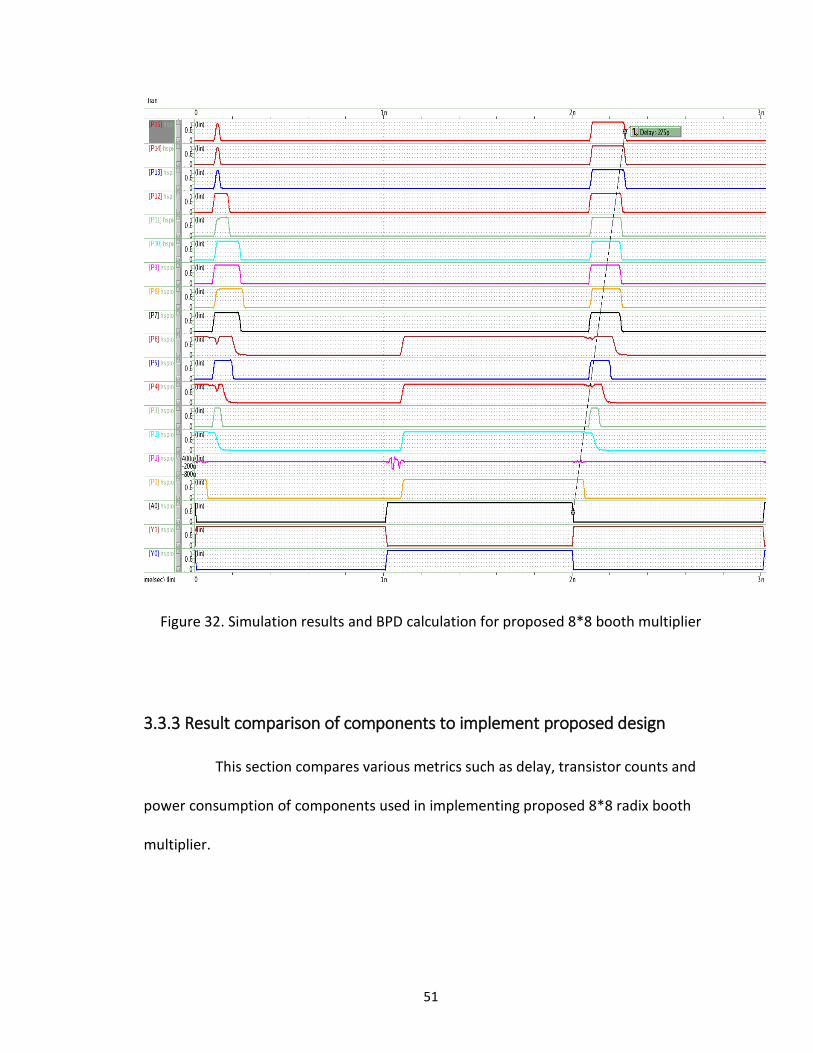
010 (00000000) and 8510 (01010101) generates the best case propagation
delay for proposed 8*8 booth multiplier. Here 00000000 is applied to multiplicand bits
and 01010101 is applied to multiplier bits. Waveform for proposed 8*8 booth multiplier
with BPD calculation is shown in figure 32. The reason for selecting above given stimuli
is because as we fed 00000000 as multiplicand bit and 010 is applied to booth encoder
of stage-1 which will produce 010 out of which 10 will select ‘2A’ and 0 at MSB will
select directly the output from 10-bit MUX 3:1.
The below discussed stimuli produces best propagation delay because in
stage-1 it does not have to wait for output from 10-bit modified BEC with inverters at
input. For stage-2, 010 is applied to booth encoder which produces 010 out of which 10
selects ‘A’ and 0 at MSB selects adder operation. Same steps are performed at stage-3
and stage-4 because same inputs are provided to booth encoder. The power
consumption of best case stimuli for proposed 8*8 booth multiplier is 0.343 milli-watt at
1 GHz.
51
Figure 32. Simulation results and BPD calculation for proposed 8*8 booth multiplier
3.3.3 Result comparison of components to implement proposed design
This section compares various metrics such as delay, transistor counts and
power consumption of components used in implementing proposed 8*8 radix booth
multiplier.

52
Table 9. Metric comparison of components
Component Transistor
count
Delay
(ps)
Power
consumption
(uW)
Booth Encoder 32 25.5 1.36
10-bit MUX 2:1 80 24 4.38
10-bit MUX 3:1 140 49.7 11.02
10-bit BEC with inv. 190 139 25.22
10-bit SQRT CSA
(RCA + RCA)
634 171 60.52
Stage - 1 442 183 49.13
Stage -2/3/4 806 208 64.38
Proposed 8*8 radix
Booth multiplier
2860 424 274.89
3.3.4 Comparing proposed Booth multiplier with other multipliers in literature
The proposed 8*8 radix-4 booth multiplier is compared for same metrics
discussed above with other 8*8 multipliers available in literature. The comparison is
stated in below as shown in table 9.

53
Table 10. Comparison of proposed booth multiplier with other multipliers
Reference - 12 Reference - 8 Proposed
Technology (nm) 90 65 32
Supply Voltage (V) 1.2 1.32 1.0
Temperature (˚C) 25 25 25
Propagation
Delay (ns)
1.96 (0.69) 1.04 (0.51) 0.42
Power
Consumption (mW)
0.3 (0.588) 0.358 (0.510) 0.275
PDP (pJ) 0.405 0.185 0.113
Reference 1 - [12]
Reference 2 - [8]
Values mentioned in the brackets are the normalized values with respect to CMOS 32nm technology
54
4.0 Conclusion and Future work
4.1 Conclusion
• The proposed design of 8x8 booth multiplier is implemented using radix-4 booth
algorithm so it uses four stages out of which 1st stage is implemented using
booth encoder, 10-bit MUX 3:1, 10-bit modified BEC and 10-bit MUX 2:1 and 2nd,
3rd and 4th stages are implemented using booth encoder, 10-bit MUX 3:1 and 10-
bit adder/sub-tractor SQRT CSA using RCA+RCA structure.
• As the input from previous block is always zero to stage-1, so there is no need of
adder/sub-tractor block in 1st stage. In this thesis, 1st stage’s adder/sub-tractor
block is replaced by 10-bit modified BEC and 10-bit MUX 2:1. By doing this we
saved power as well as area by 23.76% and 45.16% respectively with decrease in
delay by 12.02%.
• The worst-case delay of 1st stage at data rate of 1 GHz input frequency is 183
picosecond and power consumption of 49.13 micro-watt with transistor count of
442.
• Adder/Sub-tractor block of stage-2/3/4 is implemented using 10-bit SQRT CSA
with RCA+RCA structure to boost the speed of operation compared to 10-bit
SQRT CSA using RCA+BEC structure.
• The worst-case delay of stage-2/3/4 at data rate of 1 GHz input frequency is 208
picosecond and power consumption of 64.38 micro-watt with transistor count of
806.
55
• Traditional 8x8 booth multiplier uses 16-bit adder/sub-tractor blocks in each
stages. The proposed radix-4 8x8 booth multiplier is designed with 10-bit SQRT
CSA using RCA+RCA. The principle of the design is as following. Two LSB of
output of 1st stage becomes LSB of final product (i.e. P1 and P0). Similarly, two
LSB of output of 2nd and 3rd stage will become P2-P5 bits respectively. The output
of stage-4 will become P6-P15 bits of final product, which is computed by the 10-
bit SQRT CSA with RCA+RCA architecture.
• The worst-case delay of proposed 8x8 booth multiplier at data rate of 1 GHz
input frequency is 424 picosecond and power consumption of 0.274 milli-watt
with transistor count of 2860.
4.2 Future Work
Future work includes:
• Novel structures for high speed and low-power digital matched filters can be
developed based on the proposed multiplier in this thesis.
• Delay elements (i.e. register and flip-flop) are to be optimized for performance
and techniques should be developed for low-power consumption.
• Similarly adders can be implemented using new architecture which can operate
at higher speed and consume low power as well. New techniques can be
employed to adder structure so that they consume less area. The reason for
decreasing area of adder is that adders are also used in implementation of
multipliers. So the overall area consumption of DMF decreases.

56
• Resource sharing can also be implemented in booth multiplier so that area
consumption of the design decreases.
• Testing the robustness of the designs by doing PVT variations and doing Monte
Carlo analysis.

57
References
[1] S.-W. Lee and I.-C. Park, "Low-power hybrid structure of digital matched filters for direct
sequence spread spectrum systems," in International Conference on Multimedia and Expo,
ICME, 2003.
[2] N. Srisakthi, C. Rao and M. Vidya, "Implementation of code synchronization for CDMA
applications using recursive digital matched filters," in International Conference on
Communication and Signal Processing (ICCSP), 2014.
[3] O. M. V.E. Bychkov and V. Pravda, "Modern Digital Matched Filters and Correlators for
Active Radar," in International Conference on Telecommunications, and Computer Science
(TCSET) , Lviv, Ukraine, 2006.
[4] Z. Deng, Y. Yu, D. Zou, W. Guan and L. yang, "Optimization and implementation of digital
matched filters based on FPGA," in IEEE International Conference on Broadband Network
and Multimedia Technology (IC-BNMT), 2011.
[5] P. Woodward, "Probability and information theory with application to radar.," in
Pregamon Press, 1953.
[6] G. Turin, "An introduction to matched filters.," in IRE Transaction on Information Theory,
1960.
[7] A. Kumar and C. V. R. Rao, "Low-power structures of Digital Matched Filter for direct
sequence spread spectrum," in International Conference on Wireless Communication,
Signal Processing and Networking (WiSPNET), 2016.
[8] G. Kumar and S. Sahoo, "Implementation of high speed multipliers for high performance
and low power applications," in VLSI Design and Test (VDAT), Ahmedabad, 2015.
[9] Yeh and W.-C. a. C.-W. Jen, "High speed Booth encoded parallel multiplier design," in IEEE
Transactions on Computers, 2000.
[10] F. Elguibaly, "A fast parallel multiplier-accumulator using the modified Booth algorithm," in
IEEE Transactions on Circuits and Systems II: Analog and Digital Signal Processing, 2000.
[11] B. R and P. E, "Design of high speed multiplier using Modified Booth Algorithm with hybrid
carry look-ahead adder," in International Conference on Circuit, Power and Computing
Technologies, 2016.
[12] S. Asif and Y. Kong, "Performance analysis of Wallace and radix-4 Booth-Wallace
multipliers.," in Electronic System Level Synthesis Conference (ESLsyn), San Francisco, CA,
2015.

58
[13] H. Jiang, J. Han, F. Qiao and F. Lombardi, "Approximate Radix-8 Booth Multiplier for Low-
power and High-Performance Operation," in IEEE Transactions on Computers, 2015.
[14] L. Qian, C. Wang, W. Liu, F. Lombardi and J. Han, "Design and evaluation of an approximate
Wallace-Booth mulltiplier," in IEEE International Symposium on Circuits and Systems
(ISCAS), 2016.
[15] H. Guilt, "Fully iterative fast array for binary multiplication," Electronics Letters, vol. 5, no.
12, p. 263, 1969.
[16] L. Kumre, A. Somkuwar and G. Agnihotri, "Implementation of radix-4 booth multiplier
using MGDI technique," in International Conference on Microelectronics, Communications
and Renewable Energy, 2013.
[17] E. K. L. Surendran and P. R. Antony, "Implementation of fast multiplier using modified
Radix-4 booth algorithm with redundant binary adder for low energy applications," in
International Conference on Computational Systems and Communication (ICCSC),
Trivandrum, 2014.
[18] Manjunath, V. Harikiran and K. Manikanta, "Design and implementation of 16x16 modified
booth multiplier," in Online Conference on Green Engineering and Technologies (IC-GET),
Coimbatore, India, 2015.
[19] B. Gowridevi, B. Gangadevi and A. Geethamani, "Modified booth multiprecision multiplier
with scalable voltage and frequency units.," in IEEE International Conference on
Computational Intelligence and Computing Research (ICCIC), Coimbatore, 2014.
[20] R. Abhilash, S. Dubey and M. Chinnaiah, "ASIC design of signed and unsigned multipliers
using compressors," in International Conference on Microelectronics, Computing and
Communications (MicroCom), Durgapur, 2016.
[21] I.-C. P. Sung-Won Lee, "Low-power hybrid structure of digital matched filters for direct
sequence spread spectrum systems," in Multimedia and Expo, ICME, 2003.
[22] L. Mugilvannan and Ramasamy, "Low-power and area-efficient carry select adder using
modified BEC-1 converter," in International Conference on Computing, Communication and
Networking Technologies (ICCCNT), 2013.
[23] Y. He, C.-H. Chang and J. Gu, "An area efficient 64-bit square root carry select adder for
low power application," in IEEE International Symposium on Circuits and Systems (ISCAS),
2005.
[24] P. Nautiyal, P. Madduri and S. Negi, "Implementation of an ALU using modified carry select
adder for low power and area-efficient application," in International Conference on
Computer and Computational Sciences (ICCCS), Noida, India, 2015.
59
[25] R. Priya and J. S. Kumar, "Implementation and comparision of effective area efficient
architecture for CSLA," in International Conference on Emerging Trends in Computing,
Communication and Nanotechnology (ICE-CCN) , Tirunelveli, 2013.
[26] B. Ramkumar and H. M. kittur, "Low-power and Area-Efficient Carry Select Adder," in IEEE
Transaction on Very Large Scale Integration (VLSI) Systems, 2012.
[27] N. Sako, "Pass-transistor logic circuit and a method of designing thereof". United State of
America Patent US7171636, 30 January 2007.