implementation of speed efficient image processing algorithm on multi-processor system on chip...
TRANSCRIPT
International Journal of Innovative Research in Advanced Engineering (IJIRAE) ISSN: 2349-2763 Issue 01, Volume 4 (January 2017) www.ijirae.com
_________________________________________________________________________________________________ IJIRAE: Impact Factor Value – SJIF: Innospace, Morocco (2015): 3.361 | PIF: 2.469 | Jour Info: 4.085 |
Index Copernicus 2014 = 6.57 © 2014- 17, IJIRAE- All Rights Reserved Page -5
Implementation of Speed Efficient Image Processing
algorithm on Multi-Processor System on Chip (MPSoC)
Prof. Sharmik V. Admane , Prof. Jitendra B. Zalke, Prof. Manisha Das Department of Electronics Engineering
Shri Ramdeobaba College of Engineering & Management, Nagpur, India Abstract— Today’s world demand for faster, accurate and power efficient embedded devices. These devices are not only used for controlling applications, but are also expected to perform advanced applications like image processing, audio/video encoding/decoding, etc, which need more computational speed with low power. The multiprocessor systems on a chip (MPSoC) are an option to deal with these increasing computational needs. The proposed research work is based on development of the Multi-processors environment on a FPGA chip using Microblaze soft-core processor (from Xilinx Co.). Advances in FPGA technology led the implementation of such architectures in a single chip feasible and very appealing. This MPSoC environment will be used to reduce the overhead on central processor (Master). Later an Image processing application is developed to run on a Multi-processor environment and improvement in the speed of operation is observed.
Index terms—MPSoC, Microblaze, FPGA, NoC, PEs, VLSI.
I. INTRODUCTION
Today’s high-performance computing applications, such as image processing, Audio/Video signal processing, cryptography applications or bio-informatics applications, are still limited due to insufficient processing power. In former times, the approach was to increase the clock rate of a processor for speeding up the performance. But this resulted in disadvantage of higher power consumption. Nowadays, the approach has shifted toward increasing the number of processors/Processor cores instead of increasing the clock rate.
Also in majority of the real time applications, embedded processors are expected to complete its operation accurately within its deadline. If the single processor system is made to perform multiple tasks, then it operates on each task individually one after another. However if multiple processors are used, then each task can be given to different processor and parallel computation is possible. So, the amount of time required for executing the entire number of task is reduced [1] [9][12]. This is basically the motivation for development of an MPSoC environment.
An MPSoC is a multi-processor on a single silicon chip that may contain up to ten or even hundreds of processor-memory modules (PMMs). There is always misinterpretation about multi-core and multi-processor. In case of up to ten PMMs, if the memory modules are lumped together into a single first level cache that is shared between all cores then it is called a multi-core processor. However if cache memory is not shared and is available separately for each processing element, then such system is termed as Multi-processor system. The term many core architecture is used for hundreds of cores or more on a chip that are connected together by communicating bus. [10].
MPSoC have become the important necessities of fast growing technology. Faster speed along with efficiency is the ultimate requirement of embedded consumers. All these requirements are possible in small integrated chips through MPSoC. Thus MPSoC have emerged as an important class in the field of Micro-electronics and VLSI (Very Large Scale Integration). MPSoC shows an absolute method to integrate multiple processor cores on a single chip. The development phase of MPSoC environment includes five major steps:
Platform configuration; Code generation; Application development; Application mapping on to the platform; Debugging.
International Journal of Innovative Research in Advanced Engineering (IJIRAE) ISSN: 2349-2763 Issue 01, Volume 4 (January 2017) www.ijirae.com
_________________________________________________________________________________________________ IJIRAE: Impact Factor Value – SJIF: Innospace, Morocco (2015): 3.361 | PIF: 2.469 | Jour Info: 4.085 |
Index Copernicus 2014 = 6.57 © 2014- 17, IJIRAE- All Rights Reserved Page -6
Most MPSoC works focus on one such steps e.g. platform configuration or application mapping [16].According to the system architecture model, MPSoCs are classified as Homogeneous and Heterogeneous. The Homogeneous MPSoC have processors of similar architecture where as Heterogeneous have different processor architecture on same platform. The MPSoC enables design space exploration at several levels:
Network on chip (NoC): explore different routing algorithms, topologies, priorities schemes, etc; Network interface (NI): explore different service levels to guarantee Quality of Service (QoS), as injection and
admission control; Operating System (OS): evaluate different scheduling polices, Dynamic Voltage and Frequency Scaling (DVFS)
monitoring parameters, distributed memory architectures, task migration, for instance. Power dissipation: evaluate different types of processors or NoCs in terms of energy. Processing elements (PEs): evaluate different processor architectures according to the applications
requirements. Inter-board communication: Hardware modules that enable the coordination of the MPSoC from a host
computer. [17]
These design space levels are also considered to be fundamental keywords in such type of architecture. The ultimate goalhere is to develop an environment for MPSoC using Micro-blaze soft core processor. After developing the complete system, it is implemented on FPGA like Virtex-5. Application based on image processing is implemented on a Multi-processor environment. To validate the results different analysis are performed.
This paper is organized as follows: In section II, we briefly elaborate the basic building blocks of MPSoC architecture, communication links required to interconnect these processors. Section III presents Development of MPSoC Environment with the help of hardware and software tools. Section IV explores application and also provides the analysis based on the results obtained. Finally, section V presents our conclusions.
II. MULTI-PROCESSORS SYSTEM ON CHIP
A. Multi-processors Connecting two or more processors together forms multi-processor environment. Multi-Processors can communicate to hardware components through hardware adaptation, on-chip interconnects and abstraction interfaces. Thus all components together designed in a single silicon chip forms the Multi-Processor System on Chip (MPSoC) platform. Multiprocessor systems on chips (MPSoC) are not chip multiprocessors. Chip multiprocessors are components that take advantage of increased transistor densities to put more processors on a single chip, but they don’t try to leverage application needs. MPSoC are custom architectures that balance the constraints of VLSI technology with an application’s needs.
MPSoC allow multiple processes to work in parallel. It divides complete task into small modules and transfer it to process on individual processor. Thus individual processor computes the logical operation and returns the result back to the central processor. Central processor is acting as master and others as slave. Master decides the task division and assigns each module of task to different slaves. Slave in turn calculates or computes the required operation and return result to master. Master will synchronize it and display the result for user. As most of the tedious work of computation is done by slaves, overhead on the master is reduced drastically. Also the time required by slaves for computation can be utilized by master to perform other task. Hence parallel processing of multiple tasks is possible.
However sometimes multi-processors are also referred as multi-core processors. One classification of multi-core processors is based upon the type of processor cores in the package:
1) Heterogeneous multi-core processor: A heterogeneous multi-core processor is comprised of processor cores that support different ISAs (Instruction Set Architectures). A heterogeneous multi-core processor has the advantage of employing specialized processor cores designed for the task. Heterogeneous MPSoC also referred to Chip Multi-Processing or Multi (Many) Core Systems. The Heterogeneous MPSoC has different processor architecture on same platform. In other words, these systems are composed of PEs of different types, such as one or several general purpose processors, Digital Signal Processors (DSPs), hardware accelerators, peripherals and an interconnection infrastructure like a NoC [28].
2) Homogeneous multi-core processor: A homogeneous multi-core processor is comprised of processor cores that support the same ISA. Homogeneous MPSoC have processors of similar architecture. In this approach, the basic PE embeds all the elements required for a SoC: one or several processors (general purpose or dedicated), memory and peripherals. This tile is then instantiated several times, and all these instances are interconnected through a dedicated communication infrastructure [28]. Due to their good power efficiency, heterogeneous MPSoC approaches are used for portable systems, and more generally embedded systems, while homogeneous approaches are commonly used for video game consoles, desktop computers, servers and supercomputing [28].

International Journal of Innovative Research in Advanced Engineering (IJIRAE) ISSN: 2349-2763 Issue 01, Volume 4 (January 2017) www.ijirae.com
_________________________________________________________________________________________________ IJIRAE: Impact Factor Value – SJIF: Innospace, Morocco (2015): 3.361 | PIF: 2.469 | Jour Info: 4.085 |
Index Copernicus 2014 = 6.57 © 2014- 17, IJIRAE- All Rights Reserved Page -7
B. Microblaze Soft core processor:
The Microblaze embedded soft core processor is a 32-bit reduced instruction set computer (RISC) optimized for implementation in Xilinx Field Programmable Gate Array (FPGA). The Micro-Blaze soft core processor is highly configurable, allowing selecting a specific set of features required by the design. It implements Harvard architecture. It means that it has separate bus interface units for data and instruction access. Each bus interface unit is further split into a Local Memory bus (LMB) and IBM’s On-Chip Peripheral Bus (OPB). The LMB provides single-cycle access to on-chip dual port block RAM. The OPB interface provides a connection to both on-chip and off-chip peripherals and memory. The Microblaze core also provides 8 input and 8 output interfaces to Fast Simplex Link (FSL) buses. The FSL buses are unidirectional non-arbitrated dedicated communication channels. [1][13].
Figure 1: MicroBlaze Core Block Diagram [13]
The Microblaze embedded soft core provides the following features:y
Thirty-two 32-bit general purpose registers. 32-bit instruction word with three operands and two addressing modes. Separate 32-bit instruction and data buses that conform to IBM’s OPB (On chip Peripheral Bus) specification. Separate 32-bit instruction and data buses with direct connection to on-chip block RAM through a LMB (Local
Memory Bus) 32-bit address bus FSL (Fast Simplex Link) support Single issue pipeline Instruction and data cache Hardware debug logic Hardware multiplier (in Virtex-II and subsequent devices). [13]
In order to develop Multi-processor system of such soft core processors, a processor should be connected to other processor. Thus to establish a communication between their connections, communication link is required.
C. Communication link: In order to connect multiple processors, communication link is used. This link provides transmission and reception of data between the processors. Communication links can be of three basic types:-
Simplex: unidirectional link, only transmission or only reception. Half duplex: bidirectional but one at a time means either transmission or reception will be done at a time. If
transmission is complete then only reception will be possible and vice-versa. Full duplex: bidirectional, both transmission and reception is possible together depending on packet header
address.
The different types of communication busses are available with Microblaze soft core processors like FSL (Fast Simplex Link), PLB (processor local bus) Bridge.FSL, the name itself suggests that it is simplex type of link. It provides faster communication with other processors and custom hardware due to its unidirectional dedicated link.FSL buses are used as communication link between Microblaze cores. Microblaze contains eight input and eight output FSL interfaces. The FSL channels are dedicated unidirectional point-to-point data streaming interfaces. The FSL interfaces on Microblaze are 32 bits wide. Further, the same FSL channels can be used to transmit or receive either control or data words. The performance of the FSL interface can reach up to 300 MB/sec. This throughput depends on the target device itself. The FSL bus system is ideal for Microblaze-to- Microblaze or streaming I/O communications [15].

International Journal of Innovative Research in Advanced Engineering (IJIRAE) ISSN: 2349-2763 Issue 01, Volume 4 (January 2017) www.ijirae.com
_________________________________________________________________________________________________ IJIRAE: Impact Factor Value – SJIF: Innospace, Morocco (2015): 3.361 | PIF: 2.469 | Jour Info: 4.085 |
Index Copernicus 2014 = 6.57 © 2014- 17, IJIRAE- All Rights Reserved Page -8
Figure 2: FSL bus signal [15]
The FSL bus is driven by one Master and drives one Slave. The above figure 2, shows the principle of the FSL bus system and the available signals.FSL bus transmitter end represents master (M) and reception end as slave (S) for that link.Xilinx EDK provides a set of macros for reading and writing to or from an FSL link. There are two ways of reading/writing on an FSL link: blocking or non blocking [1].Master processor can send data to otherprocessor through FSL bus using set of transfer macros like putfsl and getfsl.
Figure 3: FSL interlink
a) putfsl (value, port no.): put the data from processor (master) to fsl link. b) getfsl (value, port no.): get the data from fsl link for other processor (slave).
Here ‘value’ represents the data to be send over the bus and ‘port no.’ represents the fsl port used for communication. [23][27].
III. DESIGN ENVIRONMENT FOR SINGLE AND MULTI-PROCESSOR
Soft core Multi-processor environment is implemented on Virtex 5 – XUPV5-LX110T, FPGA (Field Programmable Gate Array) [27]. The XUPV505-LX110T is a feature-rich general purpose evaluation and development platform with on-board memory and industry standard connectivity interfaces. It features the Virtex-5 XC5VLX110T device. Peripherals available on board like LED, LCD display, serial port etc can be used depending on need of the application. Also general purpose input output (GPIO) pins are available for external hardware connection.
A. Design of single processor environment in EDK: Initially single Microblaze processor system is developed with serial communication through UART (Universal Asynchronous Receiver Transmitter) shown in figure 4. The processor was Built along with block RAM, bus control PLB (processor local bus), LMB and Serial port access Using Xilinx ISE 13.1 based EDK tool; XPS (Xilinx platform studio). The small application of image processing that is edge detection followed by histogram equalization on an image is performed on the developed environment. The number of clock ticks required to perform the above operation on an image is determined by timer connected to system through software profiling. The results obtained are discussed in the next section.
Figure4: Single processor system implemented in EDK.
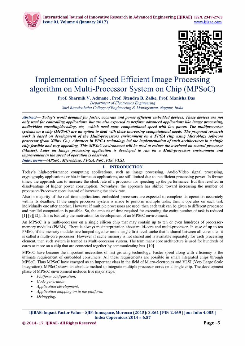
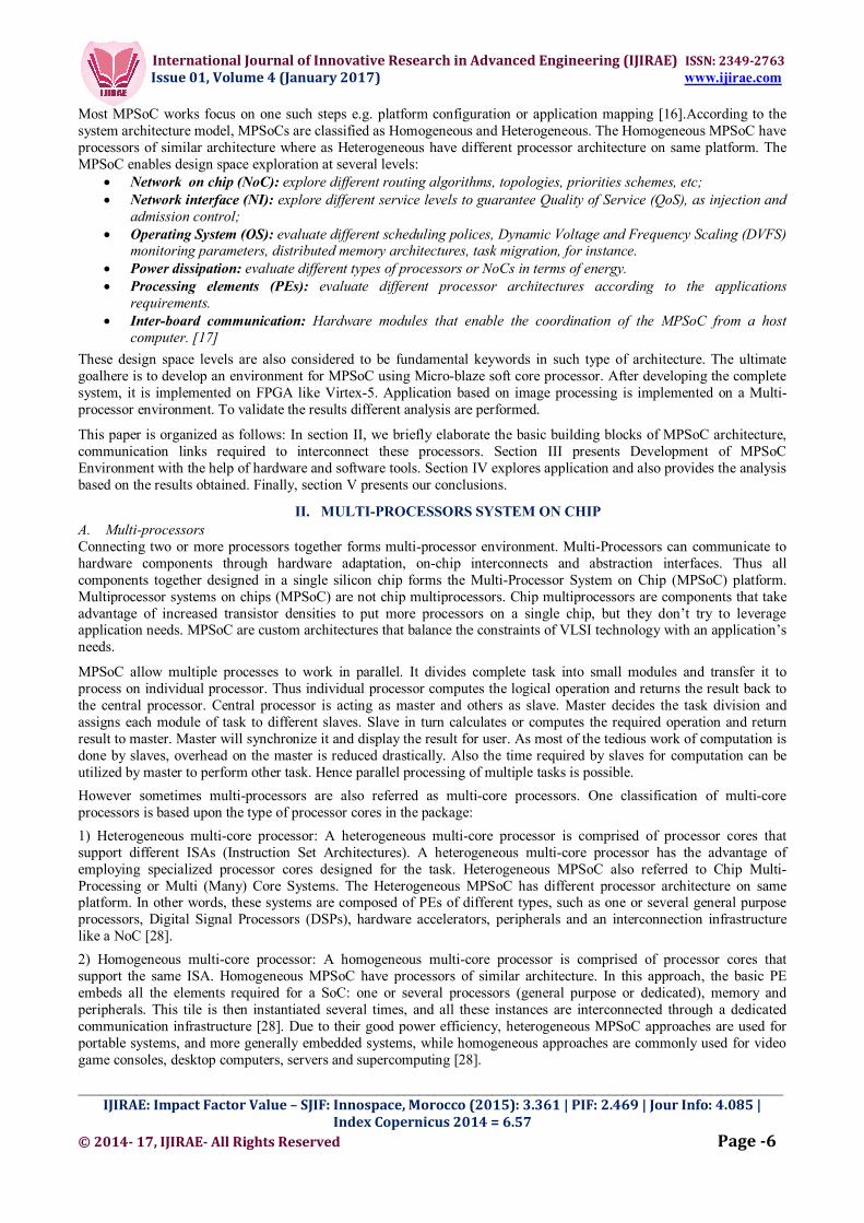
The processed image can be observed in MATLAB environment. RS232 data logger shown in figure 5 can be used to generate the .m file that needto be executed in MATLAB to display image as shown in figure 6.
International Journal of Innovative Research in Advanced Engineering (IJIRAE) ISSN: 2349-2763 Issue 01, Volume 4 (January 2017) www.ijirae.com
_________________________________________________________________________________________________ IJIRAE: Impact Factor Value – SJIF: Innospace, Morocco (2015): 3.361 | PIF: 2.469 | Jour Info: 4.085 |
Index Copernicus 2014 = 6.57 © 2014- 17, IJIRAE- All Rights Reserved Page -9
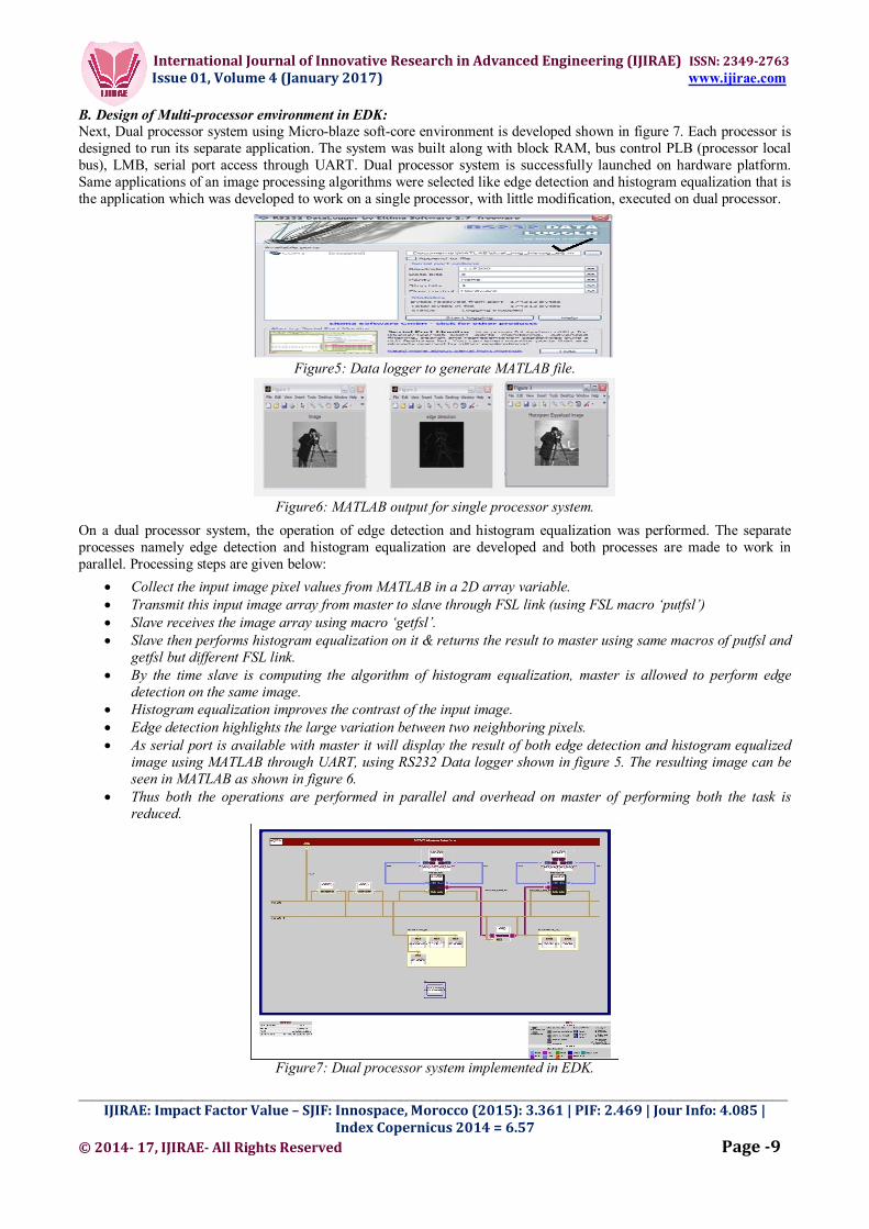
B. Design of Multi-processor environment in EDK: Next, Dual processor system using Micro-blaze soft-core environment is developed shown in figure 7. Each processor is designed to run its separate application. The system was built along with block RAM, bus control PLB (processor local bus), LMB, serial port access through UART. Dual processor system is successfully launched on hardware platform. Same applications of an image processing algorithms were selected like edge detection and histogram equalization that is the application which was developed to work on a single processor, with little modification, executed on dual processor.
Figure5: Data logger to generate MATLAB file.
Figure6: MATLAB output for single processor system.
On a dual processor system, the operation of edge detection and histogram equalization was performed. The separate processes namely edge detection and histogram equalization are developed and both processes are made to work in parallel. Processing steps are given below:
Collect the input image pixel values from MATLAB in a 2D array variable. Transmit this input image array from master to slave through FSL link (using FSL macro ‘putfsl’) Slave receives the image array using macro ‘getfsl’. Slave then performs histogram equalization on it & returns the result to master using same macros of putfsl and
getfsl but different FSL link. By the time slave is computing the algorithm of histogram equalization, master is allowed to perform edge
detection on the same image. Histogram equalization improves the contrast of the input image. Edge detection highlights the large variation between two neighboring pixels. As serial port is available with master it will display the result of both edge detection and histogram equalized
image using MATLAB through UART, using RS232 Data logger shown in figure 5. The resulting image can be seen in MATLAB as shown in figure 6.
Thus both the operations are performed in parallel and overhead on master of performing both the task is reduced.
Figure7: Dual processor system implemented in EDK.

International Journal of Innovative Research in Advanced Engineering (IJIRAE) ISSN: 2349-2763 Issue 01, Volume 4 (January 2017) www.ijirae.com
_________________________________________________________________________________________________ IJIRAE: Impact Factor Value – SJIF: Innospace, Morocco (2015): 3.361 | PIF: 2.469 | Jour Info: 4.085 |
Index Copernicus 2014 = 6.57 © 2014- 17, IJIRAE- All Rights Reserved Page -10
When master is busy performing edge detection, slave is developing a high contrast image by histogram equalization method. Thus parallel operation is achieved in dual processor system. Similarly, any time consuming task can be allotted to slave and master will have control about their execution. Transmitting data through FSL also shows that we can transfer the large data size like an image. The results obtained are discussed in the next section.
Figure8: MATLAB output for dual processor system
IV. EXPERIMENTATION RESULTS
As discussed above the single processor system is designed and an application of an image processing is executed on it. The clock ticks required to perform this operation is measured by using timer connected to the single processor system. The table (1) shows the number of cycles required to perform the edge detection followed by histogram equalization.
TABLE1: NUMBER OF CYCLES REQUIRED FOR SINGLE PROCESSOR SYSTEM. Operation Number of cycles
Image display 1,016,953,343 Histogram equalization 999,253,884 Edge detection on same image 849,400,390 Total Clock ticks Required 2,865,607,617
Again the same task of image processing but with little modification in the application is allowed to run on Dual processor system that is edge detection and histogram equalization. The number of clock ticks required to perform the above operation on an image is determined by timer connected to system through software profiling. The table (2) shows the number of cycles required to perform the edge detection and histogram equalization in parallel.
TABLE2: NUMBER OF CYCLES REQUIRED FOR DUAL PROCESSOR SYSTEM Operation Number of cycles
Image display 1,016,953,343 Image transmission to slave 9,800,399 Edge detection on same image 883,724,909* Image reception from slave 9,777,309 Histogram equalization 997,638,332* Total Clock ticks Required 2,034,169,383
*both the operationsare executed in parallel, so here considering the maximum clock cycles in calculating the total time.
As shown above,in table (1) and (2) the total no. of cycles required for single processor are 2,865,607,617 and the total no. of cycles required for dual processor is 2,034,169,383 (997,638,332 + 9,800,399 + 9,777,309 +1,016,953,343) which are less as compared to single processor. As discussed above, with dual processor system the edge detection operation takes 883,724,909 clock ticks and Histogram equalization takes 997,638,332 clock ticks and since both the operations are performing in parallel, we are considering the maximum clock cycles in calculating the total time.
Figure9: Graphical representation

International Journal of Innovative Research in Advanced Engineering (IJIRAE) ISSN: 2349-2763 Issue 01, Volume 4 (January 2017) www.ijirae.com
_________________________________________________________________________________________________ IJIRAE: Impact Factor Value – SJIF: Innospace, Morocco (2015): 3.361 | PIF: 2.469 | Jour Info: 4.085 |
Index Copernicus 2014 = 6.57 © 2014- 17, IJIRAE- All Rights Reserved Page -11
So, adding one processor to the existing single processor system shows that 29% of time could be saved. Thus operation of multiple processors shows reduction in number of clock cycles. Hence, MPSoC will make the system to operate faster. Area Utilization: As a new processor is added to the existing single processor system, numbers of logical elements required will increases. Increase in number of logic slices, flip flops and memory also depends on application. Thus increasing number of processors increases the amount of logic blocks used and also the memory consumption.
TABLE.4 AREA REQUIRED FOR SINGLE CORE PROCESSOR SYSTEM Attribute Used Total %
utilization Number of Slice Registers 7,824 69,120 11 Number of Slice LUTs: 7,327 69,120 10 Number of occupied Slices 4050 17,280 23 Number of Block RAM/FIFO
25 148 16
Total Memory used (KB) 900 5,328 16
Table.5 Area required for Dual core processor system Attribute Used Total %
utilization Number of Slice Registers 9,056 69,120 13 Number of Slice LUTs: 8,297 69,120 12 Number of occupied Slices 4,630 17,280 26 Number of Block RAM/FIFO
35 148 23
Total Memory used (KB) 1,225 5,328 23
V. CONCLUSIONS
Developing the environment for MPSoC using Micro blaze provide parallel operation of multiple processors. Thus dividing time consuming task into small modules and computing them in parallel will improve the speed of operation and reduce the overhead on master processor. Hence faster systems can be developed through MPSoC. This is verified using timing analysis that the amount of time consumption required for parallel operation of two different tasks on dual processor system, is 29% less than time required for single processing system.
Area utilization indicates that number of logical register and memory consumption increases. However amount of memory usage completely depends on application undertaken. Also increasing number of processor increases the inter-communication overhead and circuit complexity.
REFERENCES
[1]. P.Huerta, J.Castillo, J.I.Mártinez, V.López, “A MicroBlaze based Multiprocessor SoC” HW/SW Codesign Group, Universidad Rey Juan Carlos, 28933 Móstoles, Madrid Spain.
[2]. Wayne Wolf, Ahmed Amine Jerraya, and Grant Martin, “MPSoC Technology”. IEEE Transaction on computer-aided design of integrated circuits and design, 2008.
[3]. Slim BEN OTHMAN, Ahmed Karim BEN SALEM, Hedi Abdelkrim, Slim BEN SAOUO L.E.C.A.P.- E.P.T. / I.N. S.A. T. B.P. 676, 1080 Tunis Cedex, Tunisia. “MPSoC Design Approach of FPGA-based Controller for Induction Motor Drive”. 978- 1-4673-0342-21. 2012 IEEE
[4]. Tong, J.G. Anderson, I.D.L., Khalid M.A.S., “Soft-Core Processors for Embedded Systems” Microelectronics, 2006. ICM '06. International Conference (IEEE).
[5]. Hristo Nikolov, Todor Stefanov, Ed Deprettere. “Efficient external memory interface for Multi-processor platforms realized on FPGA chips” LIACS, Leiden University, The Netherlands. 2007 IEEE.
[6]. Wander O. Cesário, Damien Lyonnard, Gabriela Nicolescu, Yanick Paviot, Sungjoo Yoo, and Ahmed A. Jerraya, “Multiprocessor SoC Platforms: A Component- Based Design Approach,” TIMA Laboratory, IEEE Design & Test of Computers, 2002 IEEE.
[7]. Roberta Piscitelli and Andy D. Pimentel Computer Systems Architecture group Informatics Institute, University of Amsterdam, The Netherlands. “A High-Level Power Model for MPSoC on FPGA” 2011 IEEE International Parallel & Distributed Processing Symposium.
[8]. Joaquín Olivares, Juan Gómez, José M. Palomares, and Miguel A. Montijano University of Córdoba “Biprocessor SoC in an FPGA for Teaching Purposes” Eighth IEEE International Conference on Advanced Learning Technologies.

International Journal of Innovative Research in Advanced Engineering (IJIRAE) ISSN: 2349-2763 Issue 01, Volume 4 (January 2017) www.ijirae.com
_________________________________________________________________________________________________ IJIRAE: Impact Factor Value – SJIF: Innospace, Morocco (2015): 3.361 | PIF: 2.469 | Jour Info: 4.085 |
Index Copernicus 2014 = 6.57 © 2014- 17, IJIRAE- All Rights Reserved Page -12
[9]. Wolf, W: The Future of Multiprocessor Systems-on-chip Proceedings of the Design Automation Conference (DAC’04) 2004. pp. 681-685
[10]. Stefan Aust, Harald Richter, “Energy aware MPSoC with Space-sharing for real time apllication” in ADVCOMP 2011, Lisbon, Portugal.
[11]. Jason G. Tong, and Ian D.L. Anderson “Soft core processors for embedded systems”. Research centre for integrated micro-systems, University of Windsor.18th international conference on micro-electronics-2006.
[12]. Wolf, W: “Multimedia Applications of Multiprocessor Systems-on-Chip.” Proceedings of the Design, Automation and Test in Europe Conference (DATE’05). 2005. pp. 86-89.
[13]. MicroBlaze Processor Refrence Guide, Xilinx, http://www.xilinx.com [14]. EDK Concepts, Tools, and Techniques, Xilinx, http://www.xilinx.com [15]. LogiCORE IP Fast Simplex Link (FSL) V20 Bus (v2.11f), Xilinx, http://www.xilinx.com [16]. Eduardo W. Wächter, Carlo Lucas, Everton A. Carara, Fernando G. Moraes, “An Open-source Framework for
Heterogeneous MPSoC Generation” FACIN - PUCRS - Av. Ipiranga 6681- Porto Alegre - 90619-900 – Brazil. [17]. Eduardo Weber Wächter, Adelcio Biazi, Fernando G. Moraes, “HeMPS-S: A Homogeneous NoC-Based MPSoCs
Framework Prototyped in FPGAs,” PUCRS – FACIN – Av. Ipiranga 6681 – Porto Alegre – 90619-900 – Brazil. [18]. Diana G¨ ohringer, Michael H¨ ubner, Etienne Nguepi Zeutebouo, and J¨ urgen Becker. Research Article on
“Operating System for Runtime Reconfigurable Multiprocessor Systems” Hindawi Publishing Corporation International Journal of Reconfigurable Computing, Volume 2011, Article ID 121353,16pages doi:10.1155/2011/121353.
[19]. Tarek Darwish Sany Kabbani Acile Sleiman “Multi-Processor System Design on FPGA” the American university of Beirut. 2006.
[20]. Vasanth Asokan, “Designing Multiprocessor Systems in Platform Studio” White Paper: Xilinx Platform Studio (XPS). WP262 (v2.0) November 21, 2007.
[21]. FPGA Domain fpgadomain.blogspot.in/2010/03/soft-core-and-hard-core-processors.html. [22]. Jason Wu & Irfan Syed & Dr . John William “Kernel Preparation & uClinux BSP Installation”. [23]. Connecting Customized IP to the MicroBlaze Soft Processor Using the Fast Simplex Link (FSL) Channel Author:
Hans-Peter Rosinger. [24]. University of California, Berkeley Department of Electrical Engineering and Computer Sciences EECS150
Components and Design Techniques for Digital Systems John Wawrzynek, Shaoyi Cheng, Vincent Lee. 2013. [25]. Fpga developer “Convert an ML505 EDK project for the XUPV5” used for DDR_SDRAM configuration. [26]. Tai-Chi Lee, Mark White, and Michael Gubody “Matrix Multiplication on FPGA-Based Platform” Proceedings of
the World [27]. Congress on Engineering and Computer Science 2013 Vol I WCECS 2013, 23-25 October, 2013, USA. [28]. Xilinx, www.xilinx.com EDK to Run Xilkernel on a MicroBlaze Processor” august 11, 2010. Xilinx Virtex- 5
family overview. ‘ml50x’ schematics; “Virtex-5 FXT PowerPC 440 and MicroBlaze”. [29]. UG511 (v1.2.1) July 30, 2009. Xilkernel (v5.00.a)UG708 March 1, 2011. Xilinx Microprocessor Debugger (XMD)
Reference Guide. And “OS and Libraries Document Collection” June 9, 2013. [30]. Michael Hu¨bner l Ju¨rgen Becker "Multiprocessor System-on-Chip-Hardware Design and Tool Integration" ISBN
978-1-4419-6459-5, e-ISBN 978-1-4419-6460-1, DOI 10.1007/978-1-4419-6460-1, Springer New York Dordrecht Heidelberg London.