implementing ac-link with esai - nxp semiconductors ac-link with esai by ilan naslavsky and leonid...
TRANSCRIPT
Implementing AC-link With ESAI
by
Ilan Naslavsky andLeonid Smolyansky
Fre
esc
ale
Se
mic
on
du
cto
r, I
Freescale Semiconductor, Inc.
For More Information On This Product, Go to: www.freescale.com
nc
...
Freescale Semiconductor
© Freescale Semiconductor, Inc., 2004. All rights reserved.

Fre
esc
ale
Se
mic
on
du
cto
r, I
Freescale Semiconductor, Inc.
For More Information On This Product, Go to: www.freescale.com
nc
...

Implementing AC-link With ESAI iii
CONTENTS
1
Introduction
1.1 Scope . . . . . . . . . . . . . . . . . . . . . . . . . . . . . . . . . . . . . . . . . . . . . . . . . . . 1-11.2 AC Ô97 Digital Controller . . . . . . . . . . . . . . . . . . . . . . . . . . . . . . . . . . . 1-11.3 The AC Ô97 Digital Serial Interface (AC-link) . . . . . . . . . . . . . . . . . . . 1-2
2
Physical Connection
2.1 AC-link Lines . . . . . . . . . . . . . . . . . . . . . . . . . . . . . . . . . . . . . . . . . . . . 2-12.2 ESAI Pin Connections . . . . . . . . . . . . . . . . . . . . . . . . . . . . . . . . . . . . . 2-2
3
Data Flow
3.1 Output Data Streams . . . . . . . . . . . . . . . . . . . . . . . . . . . . . . . . . . . . . . 3-13.2 Input Data Streams . . . . . . . . . . . . . . . . . . . . . . . . . . . . . . . . . . . . . . . 3-13.3 Data Flow Model. . . . . . . . . . . . . . . . . . . . . . . . . . . . . . . . . . . . . . . . . . 3-13.4 FIFOS . . . . . . . . . . . . . . . . . . . . . . . . . . . . . . . . . . . . . . . . . . . . . . . . . . 3-23.5 Workflow . . . . . . . . . . . . . . . . . . . . . . . . . . . . . . . . . . . . . . . . . . . . . . . . 3-4
4
System Implementation
4.1 Resources. . . . . . . . . . . . . . . . . . . . . . . . . . . . . . . . . . . . . . . . . . . . . . . . 4-14.2 AC-link Application . . . . . . . . . . . . . . . . . . . . . . . . . . . . . . . . . . . . . . . 4-14.3 ESAI Usage . . . . . . . . . . . . . . . . . . . . . . . . . . . . . . . . . . . . . . . . . . . . . . 4-34.4 DMA Usage . . . . . . . . . . . . . . . . . . . . . . . . . . . . . . . . . . . . . . . . . . . . . . 4-34.4.1 Transmission . . . . . . . . . . . . . . . . . . . . . . . . . . . . . . . . . . . . . . . . . . 4-34.4.2 Reception . . . . . . . . . . . . . . . . . . . . . . . . . . . . . . . . . . . . . . . . . . . . . 4-44.5 Timer Pulse Modulation. . . . . . . . . . . . . . . . . . . . . . . . . . . . . . . . . . . . 4-44.5.1 Cold Reset . . . . . . . . . . . . . . . . . . . . . . . . . . . . . . . . . . . . . . . . . . . . 4-44.5.2 Warm Reset . . . . . . . . . . . . . . . . . . . . . . . . . . . . . . . . . . . . . . . . . . . 4-54.5.3 ATE Test Mode . . . . . . . . . . . . . . . . . . . . . . . . . . . . . . . . . . . . . . . . 4-54.5.4 Vendor-Specific Test Mode . . . . . . . . . . . . . . . . . . . . . . . . . . . . . . . 4-64.6 Interrupts . . . . . . . . . . . . . . . . . . . . . . . . . . . . . . . . . . . . . . . . . . . . . . . 4-64.6.1 Receiver Last Slot Interrupt. . . . . . . . . . . . . . . . . . . . . . . . . . . . . . 4-64.6.2 Timer Compare Interrupt . . . . . . . . . . . . . . . . . . . . . . . . . . . . . . . . 4-74.6.3 DMA Channel 0 Interrupt . . . . . . . . . . . . . . . . . . . . . . . . . . . . . . . 4-74.7 Assumptions And Recommendations . . . . . . . . . . . . . . . . . . . . . . . . . 4-8
Fre
esc
ale
Se
mic
on
du
cto
r, I
Freescale Semiconductor, Inc.
For More Information On This Product, Go to: www.freescale.com
nc
...

iv Implementing AC-link With ESAI
5
ESAI, DMA, and Timer Configuration
5.1 ESAI Configuration . . . . . . . . . . . . . . . . . . . . . . . . . . . . . . . . . . . . . . . . 5-15.1.1 Transmit Clock Control Register (TCCR). . . . . . . . . . . . . . . . . . . . 5-15.1.2 Transmit Control Register (TCR) . . . . . . . . . . . . . . . . . . . . . . . . . . 5-25.1.3 Receive Clock Control Register (RCCR) . . . . . . . . . . . . . . . . . . . . . 5-35.1.4 Receive Control Register (RCR) . . . . . . . . . . . . . . . . . . . . . . . . . . . 5-45.1.5 Common Control Register (SAICR). . . . . . . . . . . . . . . . . . . . . . . . . 5-55.1.6 Port Control, Direction and Data Registers . . . . . . . . . . . . . . . . . . 5-55.2 DMA Configuration - Channel 0. . . . . . . . . . . . . . . . . . . . . . . . . . . . . . 5-75.2.1 DMA Control Register for Channel 0 (DCR0) . . . . . . . . . . . . . . . . 5-75.2.2 DMA Counter Register for Channel 0 (DCO0) . . . . . . . . . . . . . . . . 5-85.2.3 DMA Offset Registers (DOR0 and DOR1) . . . . . . . . . . . . . . . . . . . 5-85.2.4 DMA Source Address Register for Channel 0 (DSR0) . . . . . . . . . . 5-85.2.5 DMA Destination Address Register for Channel 0 (DDR0). . . . . . 5-85.3 DMA Configuration - Channel 1. . . . . . . . . . . . . . . . . . . . . . . . . . . . . . 5-85.3.1 DMA Control Register for Channel 1 (DCR1) . . . . . . . . . . . . . . . . 5-85.3.2 DMA Counter Register for Channel 1(DCO1) . . . . . . . . . . . . . . . . 5-95.3.3 DMA Offset Registers (DOR2 and DOR3) . . . . . . . . . . . . . . . . . . . 5-95.3.4 DMA Source Address Register for Channel 1(DSR1) . . . . . . . . . . 5-95.3.5 DMA Destination Address Register for Channel 1 (DDR1). . . . . . 5-95.4 Timer Configuration . . . . . . . . . . . . . . . . . . . . . . . . . . . . . . . . . . . . . . . 5-95.4.1 Timer Control/Status Register (TCSR) . . . . . . . . . . . . . . . . . . . . . 5-105.4.2 Timer Load Register (TLR) . . . . . . . . . . . . . . . . . . . . . . . . . . . . . . 5-105.4.3 Timer Compare Register (TCPR) . . . . . . . . . . . . . . . . . . . . . . . . . 5-10
APPENDIXES:
Appendix A Code and Equates
Appendix B References
Fre
esc
ale
Se
mic
on
du
cto
r, I
Freescale Semiconductor, Inc.
For More Information On This Product, Go to: www.freescale.com
nc
...

Implementing AC-link With ESAI v
FIGURES
Figure 2-1 ESAI - AC Õ97 Connection: The AC_Link . . . . . . . . . . . . . . . . . 2-2
Figure 3-1 Audio Application-CODEC Interaction Model . . . . . . . . . . . . . 3-3
Figure 3-1 AC-link Application Data Flow . . . . . . . . . . . . . . . . . . . . . . . . 3-4
Figure 4-1 AC-Link Implementation . . . . . . . . . . . . . . . . . . . . . . . . . . . . . 4-2
Figure 4-1 AC Ô97 Cold Reset. . . . . . . . . . . . . . . . . . . . . . . . . . . . . . . . . . . . 4-5
Figure 4-1 AC Ô97 Warm Reset . . . . . . . . . . . . . . . . . . . . . . . . . . . . . . . . . . 4-5
Figure 4-1 AC Ô97 ATE Test Mode. . . . . . . . . . . . . . . . . . . . . . . . . . . . . . . . 4-6
Figure 4-1 Buffer Swapping . . . . . . . . . . . . . . . . . . . . . . . . . . . . . . . . . . . . 4-7
Figure 5-1 Transmit Clock Control Register (TCCR). . . . . . . . . . . . . . . . . 5-1
Figure 5-2 Transmit Control Register (TCR) . . . . . . . . . . . . . . . . . . . . . . . 5-2
Figure 5-3 Receive Clock Control Register (RCCR) . . . . . . . . . . . . . . . . . . 5-3
Figure 5-4 Receive Control Register (RCR) . . . . . . . . . . . . . . . . . . . . . . . . 5-4
Figure 5-5 Common Control Register (SAICR) . . . . . . . . . . . . . . . . . . . . . 5-5
Fre
esc
ale
Se
mic
on
du
cto
r, I
Freescale Semiconductor, Inc.
For More Information On This Product, Go to: www.freescale.com
nc
...

vi Implementing AC-link With ESAI
Fre
esc
ale
Se
mic
on
du
cto
r, I
Freescale Semiconductor, Inc.
For More Information On This Product, Go to: www.freescale.com
nc
...

Implementing AC-link With ESAI vii
TABLES
Table 2-1 AC-link Signals . . . . . . . . . . . . . . . . . . . . . . . . . . . . . . . . . . . . . 2-1
Table 3-1 AC-link Application Workflow . . . . . . . . . . . . . . . . . . . . . . . . . 3-5
Table 5-1 PCR, PRR and PDR Values . . . . . . . . . . . . . . . . . . . . . . . . . . . 5-6
Table A-1 Data X-Memory Usage . . . . . . . . . . . . . . . . . . . . . . . . . . . . . . . A-1
Table A-2 Data Y-Memory Usage. . . . . . . . . . . . . . . . . . . . . . . . . . . . . . . . A-2
Table A-3 FIFO Table, Initial Status . . . . . . . . . . . . . . . . . . . . . . . . . . . . A-2
Fre
esc
ale
Se
mic
on
du
cto
r, I
Freescale Semiconductor, Inc.
For More Information On This Product, Go to: www.freescale.com
nc
...

viii Implementing AC-link With ESAI
Fre
esc
ale
Se
mic
on
du
cto
r, I
Freescale Semiconductor, Inc.
For More Information On This Product, Go to: www.freescale.com
nc
...

Introduction
Implementing AC-link with ESAI
1-1
1 Introduction
The Enhanced Serial Audio Interface (ESAI) of the DSP56300 Family provides full capabilities for interfacing with a general AC Ô97 CODEC through an AC Ô97 Digital Serial Interface, the AC-link.
The DSP56362 is the first DSP56300 Family derivative that presents the ESAI and is readily enabled to run this application.
Appendix B
lists reference materials pertaining to the DSP56300 Family, the DSP56362, and the
Audio CODEC Ô97 Component Specification
.
1.1 Scope
This application report describes how to implement an AUDIO CODEC Ô97 Digital Serial Interface (AC-link) using the ESAI. It is recommended for developers who have previous knowledge of MotorolaÕs DSP56300 Family of Digital Signal Processors and of the AC Ô97 Component Specification.
Section 2
describes the physical connection between ESAI and an AC Ô97 CODEC.
Section 3
describes the Data-Flow model.
Section 4
delineates the system concept implemented in the AC-link application.
Section 5
details the configuration of DSP56300 Family resources used in this application.
Appendix A
shows the assembly code and equates of the application.
Appendix B
lists relevant reference information.
1.2 AC ‘97 Digital Controller
The AC Ô97 Digital Controller runs one or more audio applications and exchanges data with its analog counterpart, the AC Ô97 CODEC, through the AC-link. The DSP56300 Family may implement the AC Ô97 Digital Controller functionality.
Fre
esc
ale
Se
mic
on
du
cto
r, I
Freescale Semiconductor, Inc.
For More Information On This Product, Go to: www.freescale.com
nc
...

1-2
Implementing AC-link with ESAI
Introduction
1.3 The AC ‘97 Digital Serial Interface (AC-link)
AC Ô97 Digital Serial Interface, the AC-link, provides point-to-point, two-way communication between an AC Ô97 Digital Controller and an AC Ô97 CODEC. Data exchange is performed over two Time Division Multiplexed (TDM) one-wire channels, one in each direction, supported by two additional timing signals and a hardware reset line.
This report presents an AC-link application for a DSP56300 Family derivative. The application performs all specified AC-link tasks, providing audio applications with a straightforward and modular interface.
Fre
esc
ale
Se
mic
on
du
cto
r, I
Freescale Semiconductor, Inc.
For More Information On This Product, Go to: www.freescale.com
nc
...

Physical Connection
Implementing AC-link with ESAI
2-1
2 Physical Connection
This section describes the physical connection between the Enhanced Serial Audio Interface (ESAI) and a generic AC Ô97-compatible CODEC. The AC Ô97 DSI or AC-link implementation suggested in this application report uses seven ESAI pins, providing the whole AC-link functionality. This section describes this glueless connection.
2.1 AC-link Lines
Five lines make up the AC-link. On the DSP side, all of the lines are connected to ESAI pins. In some cases, these lines are programmed as GPIO pins in order to accomplish a particular signalÕs characteristic.
Table 2-1
briefly describes their function and direction related to the ESAI
.
The AC-link lines should be connected to the CODEC according to specification.
Table 2-1
AC-link Signals
Signal Description Direction
BIT_CLK Serial bit-clock @12.288MHz input
SYNC Frame Sync signal @48kHz; high for 16 BIT_CLK periods, low for 240
output
SDATA_IN Serial Data Stream input
SDATA_OUT Serial Data Stream output
RESET Asynchronous Hardware Reset output
Fre
esc
ale
Se
mic
on
du
cto
r, I
Freescale Semiconductor, Inc.
For More Information On This Product, Go to: www.freescale.com
nc
...

2-2
Implementing AC-link with ESAI
Physical Connection
2.2 ESAI Pin Connections
Figure 2-1
outlines the ESAI-CODEC pin connections.
Figure 2-1
ESAI - AC Õ97 Connection: The AC_Link
As
Figure 2-1
shows, the AC Ô97 controller drives an asynchronous hardware reset signal through the RESET line. The ESAI P10 pin (SDO1) is configured as a GPIO pin and driven low with each RESET signal.
Section 4
of this application report gives a more detailed description of the AC Ô97 reset signaling implementation.
A Serial Data Output line,
SDATA_OUT
, is provided at the ESAI P11 pin and is configured as the ESAI #0 transmitter output (SDO0). Eventually, this pin may be temporarily reconfigured as GPIO, permitting the DSP to signal the AC Ô97 CODEC to enter ATE Test Mode.
BIT_CLK
DSP56300 AC ’97
SDATA_IN
RESET
SYNC
SDATA_OUT
SCKT
SDO5/SDI0
SDO1
FST
SDO0
SCKR
FSR
(AC ‘97 Digital Controller)CODEC
DERIVATIVEwith ESAI
AA1559
Fre
esc
ale
Se
mic
on
du
cto
r, I
Freescale Semiconductor, Inc.
For More Information On This Product, Go to: www.freescale.com
nc
...

Physical Connection
Implementing AC-link with ESAI
2-3
The Frame Sync signal (SYNC) is generated by the transmitter side of ESAI and is output through its P4 pin, conÞgured as Frame Sync for Transmitter (FST). In order to comply with the timing constraints of the AC Ô97 and DSP56300 Family, the ESAI transmitter and receiver are programmed to work asynchronously. Therefore, Frame Sync must be fed for the receiver side as well. Thus, a feedback connection between FST, output conÞgured, and the ESAI P1 pin (Frame Sync for Receiver - FSR), input configured, is needed. This pin can be reconfigured temporarily as GPIO, permitting the DSP to signal the AC Ô97 CODEC to enter the Vendor-Specific Test mode.
Similarly, the serial data clock provided by the AC Ô97 CODEC, (
BIT_CLK
), must be fed for both the transmitter and receiver portions of ESAI. The required connection links the
BIT_CLK
line through the ESAI P0 and P3 pinsÑReceiver Serial Clock (SCKR) and Transmitter Serial Clock (SCKT), respectivelyÑare both configured as input.
The Serial Data Input line,
SDATA_IN
, is supplied by the AC Ô97 CODEC, driving the ESAI P6 Serial Transmit/Receive Data pin, SDO5/SDI0, and conÞgured as the ESAI #0 receiver input.
Fre
esc
ale
Se
mic
on
du
cto
r, I
Freescale Semiconductor, Inc.
For More Information On This Product, Go to: www.freescale.com
nc
...

2-4
Implementing AC-link with ESAI
Physical Connection
Fre
esc
ale
Se
mic
on
du
cto
r, I
Freescale Semiconductor, Inc.
For More Information On This Product, Go to: www.freescale.com
nc
...

Data Flow
Implementing AC-link with ESAI
3-1
3 Data Flow
This section describes the AC-link application data-flow model, which is an implementation with a five-slot-output and a six-slot-input. This modular concept enables a smooth upgrade for a larger number of data streams.
Two Time-Division-Multiplexed (TDM) one-wire data channels constitute the AC-link data path, one channel for each direction. Each channel can transfer up to 12 data streams, plus a leading validation stream.
3.1 Output Data Streams
The AC-link implementation defines three output data streams that demand five slots of the TDM output channel:
¥
PCM Playback
: two-channel composite PCM stream, 2 slots
¥
Control
: control register write port, 2 slots
¥
Modem Line CODEC Output
: modem line CODEC DAC input stream, 1 slot
3.2 Input Data Streams
In the input direction, the AC-link implementation defines four data streams that demand six slots of the TDM input channel:
¥
PCM Record
: two-channel composite PCM stream, 2 slots
¥
Status:
control register read port, 2 slots
¥
Modem Line CODEC Input
: modem line CODEC ADC output stream, 1 slot
¥
Dedicated Microphone Input
: dedicated microphone input stream, 1 slot
3.3 Data Flow Model
The AC Ô97 Digital Controller sees the AC-link data path as two sets of software implemented as First-In-First-Out queues (FIFOs). Each set reflects one direction of the link, being composed by one FIFO for every data stream, summing up three output FIFOs and four input FIFOs in this particular implementation.
Fre
esc
ale
Se
mic
on
du
cto
r, I
Freescale Semiconductor, Inc.
For More Information On This Product, Go to: www.freescale.com
nc
...

3-2
Implementing AC-link with ESAI
Data Flow
When the Digital Controller has data from any of the three output streams to send to the CODEC, it writes it to the corresponding FIFO. Similarly, each time data from any of the four available input data streams is to be processed, the application reads it from the respective FIFO.
The data transfer path between the FIFOs and the CODEC is transparent to the audio application. This path is achieved through the AC-link application described in this section and the resources and routines detailed in
Section 4
and
Section 5
.
3.4 FIFOS
Every input and output data stream has a corresponding FIFO. The lengths of the FIFOs depend on application throughput and the demand of the corresponding type of data and are independently programmable.
Output FIFOs are read by the AC-link application once per AC Ô97 Audio Frame, i.e. 48K times per second. Data read from the FIFO is sent through the AC-link. The audio application tailors its data throughput to both the FIFOs capacity and the AC-link transfer frequency, addressing the boundary case of full FIFOs to avoid FIFO overflow. Empty FIFOs are handled by the AC-link application as if their data is not valid, although different approaches can be used with minimal code modification.
In the opposite direction, the AC-link application writes to input FIFOs at the same frequency, 48K times per second. It is the audio applicationÕs responsibility to keep input FIFOs under a not-full status, reading data at a compatible frequency. The AC-link Application enters a
crash
routine when any FIFO is full at the moment it tries to write to it. The crash routine procedure should be determined by the Audio Application specification.
Figure 3-1
describes the audio application-CODEC interaction model.
Fre
esc
ale
Se
mic
on
du
cto
r, I
Freescale Semiconductor, Inc.
For More Information On This Product, Go to: www.freescale.com
nc
...
Data Flow
Implementing AC-link with ESAI
3-3
Figure 3-1
Audio Application-CODEC Interaction Model
AC-LINK
AC ‘97 CODEC
DSP56300 FAMILY DERIVATIVE AC ‘97 DIGITAL CONTROLLER
AUDIO APPLICATION
AC-LINK APPLICATION
PCMPCM CNTRLSTAT MDMMDMMIC
INPUT FIFOS
OUTPUT FIFOS
MDM: MODEM LINE FIFO
MIC: MICROPHONE FIFO
PCM: PCM FIFO
CNTRL: CONTROL FIFO
STAT: STATUS FIFO
AA1560
Fre
esc
ale
Se
mic
on
du
cto
r, I
Freescale Semiconductor, Inc.
For More Information On This Product, Go to: www.freescale.com
nc
...

3-4
Implementing AC-link with ESAI
Data Flow
3.5 Workflow
The AC-link application handles data flow between an audio application running on a DSP56300 Derivative and an AC Ô97 CODEC. It prepares and validates data to be transmitted through the AC-link. A pair of output buffers and a pair of input buffers are allocated for transmission and reception, respectively.
Figure 3-1
AC-link Application Data Flow
output buffers (OB)
input FIFOs
currentlybeingtransferred
to betransferredafter swap
buffer swapping
OB0
OB1
IB0
IB1
input buffers (IB)
output FIFOs
AC-link
AC-LINK APPLICATION
ACTIVE BUFFER: DATA CURRENTLY BEING TRANSFERRED THROUGH AC-LINK
NOT-ACTIVE BUFFER: CURRENTLY BEING FILLED BY THE AC-LINK APPLICATION
AA1561
Fre
esc
ale
Se
mic
on
du
cto
r, I
Freescale Semiconductor, Inc.
For More Information On This Product, Go to: www.freescale.com
nc
...

Data Flow
Implementing AC-link with ESAI
3-5
As
Figure 3-1
shows, during every AC Ô97 Audio Frame one of the output buffers is
active
, meaning its data is currently being transmitted. At the same time, the second buffer is not-active, and is fed by the AC-link application with the output FIFOs data. Slot validationÑthat is, slot 0 determination (Audio Frame TAG)Ñis accomplished concurrently. In the course of the subsequent audio frame, the buffers roles switch.
A symmetrical scheme is adopted in the reception section. The
active
buffer is filled with AC-link incoming data, while the data of the not-active buffer is transferred to input FIFOs. Reception buffers alternate active and not-active states in the same way as the transmitter buffers.
The first and second transmitted frames data after the AC-link reset (F
0
, F
1
) are entirely invalidated in order to enable the AC-link Application to enter the steady state.
Table 3-1
outlines the buffer swapping procedure.
Table 3-1
AC-link Application Workflow
Transmission Section Reception Section
Frame Active Buffer(Buffer -> ESAI)
Not (FIFO -> Buffer)
Active Buffer(ESAI -> Buffer)
Not Active Buffer (Buffer -> FIFO)
F
0
B1(-1)(whole buffer invalidated)
-(no RLS int. occurred)
B1(0) -(no RLS int. occurred)
F
1
B0 (whole buffer invali-dated)
B1(1) B0(1) B1(0)
F
2
B1(1)(Þrst valid buffer transmitted)
B0(2) B1(2) B0(1)
... ... ... ... ...
F
t-2
B1(t-3) B0(t-2) B1(t-2) B0(t-3)
F
t-1
B0(t-2) B1(t-1) B0(t-1) B1(t-2)
F
t
B1(t-1) B0(t) B1(t) B0(t-1)
F
t+1
B0(t) B1(t+1) B0(t+1) B1(t)
F
t+2
B1(t+1) B0(t+2) B1(t+2) B0(t+1)
... ... ... ... ...
Fre
esc
ale
Se
mic
on
du
cto
r, I
Freescale Semiconductor, Inc.
For More Information On This Product, Go to: www.freescale.com
nc
...
3-6
Implementing AC-link with ESAI
Data Flow
Fre
esc
ale
Se
mic
on
du
cto
r, I
Freescale Semiconductor, Inc.
For More Information On This Product, Go to: www.freescale.com
nc
...

System Implementation
Implementing AC-link with ESAI
4-1
4 System Implementation
This section describes the system concept implemented in this application. The AC-link application is implemented with a set of DSP56300 derivative routines that supports ESAI in its AC Ô97 mode, handling several on-chip resources.
4.1 Resources
The implemented application uses the following resources of the DSP56300 derivative:
¥ 1 ESAI transmitter
¥ 1 ESAI receiver
¥ 2 Direct Memory Access (DMA) channels
¥ 1 timer module
¥ Variable quantity of internal data memory for buffers and FIFOs
4.2 AC-link Application
The AC-link application implements an AC Ô97 Digital Interface using ESAI on its AC Ô97 mode and is supported by two DMA channels and a timer module.
Figure 4-1
presents the application block diagram.
The ESAI performs AC-link Audio Frame multiplexing and demultiplexing, as well as timing and control functions. DMA channels transfer data between the ESAI and the audio application running on the DSP56300 derivative. A timer module is necessary in AC-link special signaling.
Fre
esc
ale
Se
mic
on
du
cto
r, I
Freescale Semiconductor, Inc.
For More Information On This Product, Go to: www.freescale.com
nc
...
4-2
Implem
enting AC
-link with E
SAI
System
Imp
lemen
tation
Figu
re 4-1
AC
-link Im
plemen
tation
DATA
MEMORY
(FIFOs and
DSP56300 DERIVATIVE
DSP56300 CORE
CONTROLTIMING
SDATA_OUT
SDATA_IN
DMA #0
ESAI
TIMER
AC ‘97
DMA #1
COMPATIBLE
CODEC
BUFFERS)
AA1562
Fre
esc
ale
Se
mic
on
du
cto
r, I
Freescale Semiconductor, Inc.
For More Information On This Product, Go to: www.freescale.com
nc
...

System Implementation
Implementing AC-link with ESAI
4-3
4.3 ESAI Usage
The ESAI is programmed to transmit with TX #0 and receive with RX #0 in asynchronous mode:
¥ with an external clock
¥ under AC Ô97 mode
¥ with 12
×
20-bit slots per frame plus a leading 16-bit slot (slot 0, Tag Phase).
The external clock for both the receiver and transmitter is the
BIT_CLK
signal generated by the AC Õ97 CODEC. The transmitter section generates the frame synchronization signal (FST/SYNC) supplied to the CODEC and to the receiver section. FST is driven with the falling edge of
BIT_CLK
, one bit before the beginning of the first slot in the frame.
In AC Õ97 mode, frame sync is generated high for the first word, a 16-bit word corresponding to the AC Õ97 tag phase, and low for 12 words, each being one of the 20-bit slots of the AC Õ97 data phase.
Data is driven out (
SDO0/SDATA_OUT
) at the falling edge of
BIT_CLK
, being sampled by the CODEC on the
next
falling edge. Input data (
SDO5/SDI0/ SDATA_IN
) is driven by the CODEC with the rising edge of
BIT_CLK
and sampled by the receiver on the subsequent falling edge.
4.4 DMA Usage
The DMA performs data transfer between the Audio application and ESAI using one channel for each direction. DMA channel #0 transfers output data, and channel #1 transfers input data.
4.4.1 Transmission
The ESAI specification requires that the first transmitted word be written to the ESAI transmitter register by a DSP Core move
before
transmitter enabling. Accordingly, the first transmitted audio frame requires a DMA configuration in which only the data phase is transferred from the active output buffer to the ESAI. The tag phase (slot 0) is programmed as first data for the ESAI transmitter.
From the second frame on, DMA is re-programmed to work in a continuous mode, servicing the ESAI transmitter upon request and transferring both tag and data
Fre
esc
ale
Se
mic
on
du
cto
r, I
Freescale Semiconductor, Inc.
For More Information On This Product, Go to: www.freescale.com
nc
...
4-4
Implementing AC-link with ESAI
System Implementation
phases. The current active output buffer is always being accessed by DMA, while the not-active output buffer is updated and validated by the core. In steady state, DMA demands no interrupt servicing, synchronously swapping output buffers without core interference.
4.4.2 Reception
On the reception side, DMA is programmed to work in a continuous mode from the first frame, transferring both tag and data phases from the ESAI receiver register to the active input buffer and servicing the ESAI receiver upon request. The current active input buffer is always being accessed by DMA while the core transfers the not-active input buffer to the FIFOs. DMA demands no interrupt servicing and synchronously swaps input buffers without core interference.
4.5 Timer Pulse Modulation
Cold Reset, Warm Reset, ATE Test Mode and Vendor-Specific Test Mode signaling are implemented through the ESAI pins, re-programmed as GPIO. Specific signal generation is attained with the timer module.
4.5.1 Cold Reset
Cold Reset pulse is achieved by bringing the ESAI P10 pin (SDO1/RESET) low for 1.0
µ
s or more. This pin remains constantly configured as a GPIO output, as discussed in
Section 2
.
The timer module is programmed to count a number of internal clocks sufficient to produce the specified pulse (> 1.0
µ
s). The pin is driven low with timer enabling; upon a Timer Compare Interrupt that corresponds to the end of counting, the pin is brought back high.
Fre
esc
ale
Se
mic
on
du
cto
r, I
Freescale Semiconductor, Inc.
For More Information On This Product, Go to: www.freescale.com
nc
...

System Implementation
Implementing AC-link with ESAI
4-5
Figure 4-1
AC Ô97 Cold Reset
4.5.2 Warm Reset
A similar pulse generation mechanism, supported by the timer module, is used for Warm Reset. This time the timer module is programmed to count to a typical 1.3
µ
s. Re-programming the ESAI P4 pin (FST/SYNC) as GPIO output allows a high pulse to be produced on this pin. The pin is driven high with timer enabling. Upon a timer Compare Interrupt that corresponds with the end of counting, the pin is brought back low.
Figure 4-1
AC Ô97 Warm Reset
4.5.3 ATE Test Mode
ATE Test Mode signaling uses the ESAI P11 pin (
SDO0
/
SDATA_OUT
).
SDATA_OUT
must be sampled high at the trailing edge of the RESET signal. This signaling is achieved by configuring the ESAI P11 pin as GPIO output and bringing it high with timer enabling for reset pulse counting. Upon a Timer Compare Interrupt and subsequent deassertion of RESET, the pin is kept high.
RESET(SDO1)
BIT_CLK
>1.0µs >162.8nS
AA1563
SYNC(FST)
BIT_CLK
1.3 µs (Typ.) >162.8 ns
AA1564
Fre
esc
ale
Se
mic
on
du
cto
r, I
Freescale Semiconductor, Inc.
For More Information On This Product, Go to: www.freescale.com
nc
...

4-6
Implementing AC-link with ESAI
System Implementation
Figure 4-1
AC Ô97 ATE Test Mode
4.5.4 Vendor-Specific Test Mode
Vendor-Specific Test Mode is implemented equivalently to ATE Test Mode. The ESAI P4 (FST/SYNC) pin is used instead of P11.
4.6 Interrupts
Some of the AC-link application functions use program interrupts. The following paragraphs describe their usage.
4.6.1 Receiver Last Slot Interrupt
Not-Active/Active buffer swapping occurs once every Audio Frame, at the ESAI Receiver Last Slot Interrupt (RLSI). This interrupt occurs at the end of the last slot of frame F
t-1
when the ESAI finishes transmitting the last word of the output buffer and receiving the last word for input buffer, respectivelyÑfor example, OB0 and IB0. During frame F
t
, the AC-link Application continues to supply data to ESAI from the OB1 transmission buffer, while transferring received data from ESAI to IB1 through DMA transfers.
During the interrupt at frame F
t
, active buffers are switched from I/OB0 to I/OB1 and
vice versa
. Then the AC-link application fills up the not-active transmission buffer OB0 (in case any of the output FIFOs is not empty) validating the
RESET
SDATA_IN, BIT_CLK
SDATA_OUT
HI-Z
>15 ns <25 ns
AA1565
Fre
esc
ale
Se
mic
on
du
cto
r, I
Freescale Semiconductor, Inc.
For More Information On This Product, Go to: www.freescale.com
nc
...

System Implementation
Implementing AC-link with ESAI
4-7
corresponding valid-bits of the OB0 TAG (slot 0). The new OB0 buffer data is transmitted next time OB0 is active, i.e. during F
t+1
. Similarly, input FIFOs are written with data from valid slots received during F
t-1
and allocated at IB0.
Figure 4-1
Buffer Swapping
4.6.2 Timer Compare Interrupt
A Timer Compare interrupt occurs when the timer counter matches the compare register and permits the completion of the AC Ô97 reset and test signaling.
4.6.3 DMA Channel 0 Interrupt
Because of the special transmission at the first frame, the DMA Channel 0 interrupt is needed to enable DMA re-programming to work in a continuous mode. This re-programming includes disabling this interrupt.
I/OB0 I/OB1 I/OB0
(LAST SLOT INTERRUPT)
F t-1 Ft F t+1
NOTE: Timing representation out of scale.
ACTIVE BUFFERS
SYNC
AA1566
Fre
esc
ale
Se
mic
on
du
cto
r, I
Freescale Semiconductor, Inc.
For More Information On This Product, Go to: www.freescale.com
nc
...

4-8
Implementing AC-link with ESAI
System Implementation
4.7 Assumptions And Recommendations
The audio application developer should take into account some assumptions and recommendations made for this implementation:
¥ Once an RLSI interrupt occurs it must be fully serviced before the next occurrence of the same interrupt. This guarantees the completion of buffer swap, including data update and validation, avoiding DMA switching access to an out-of-date buffer. Therefore, a coherent Interrupt Priority Level setting is required.
¥ The active buffer and not-active buffer should be located in different RAM-memory modules (256 words module) in order to avoid CORE-DMA contention.
¥ The FIFOs and Buffers base addresses should comply with modulo addressing conditions in order to allow implemented routines to work properly.
¥ A case might exist when an external buffer is needed in order to delay the
SDATA_IN
signal. In the
Audio Codec Õ97 Component Specification
, data hold-time (both
SDATA_IN
and
SDATA_OUT
) from the falling edge of
BIT_CLK
is stated as 5 nsec, measured from the beginning of the edge. If
BIT_CLK
fall time is to be considered in its worst case, 6 nsec, there is an effective -1 nsec hold-time, meaning data are not stable in the falling edge. Refer to the data sheet of the particular ACÕ97 device, or contact the vendor in order to decide on external buffer needs.
Fre
esc
ale
Se
mic
on
du
cto
r, I
Freescale Semiconductor, Inc.
For More Information On This Product, Go to: www.freescale.com
nc
...
ESAI, DMA, and Timer Configuration
Implementing AC-link with ESAI
5-1
5 ESAI, DMA, and Timer Configuration
This section details how the resources to be used, ESAI, DMA, and Timer, are configured.
5.1 ESAI Configuration
The following paragraphs describe ESAI configuration and control register programming.
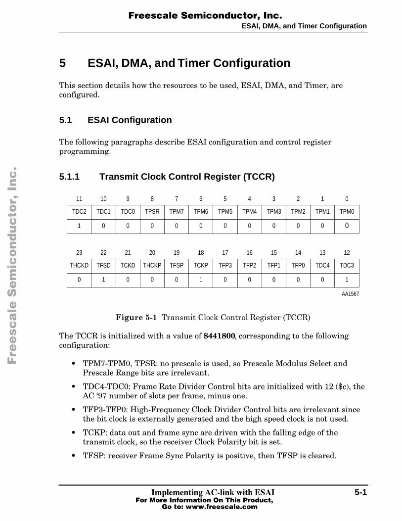
5.1.1 Transmit Clock Control Register (TCCR)
Figure 5-1
Transmit Clock Control Register (TCCR)
The TCCR is initialized with a value of
$441800
, corresponding to the following configuration:
¥ TPM7-TPM0, TPSR: no prescale is used, so Prescale Modulus Select and Prescale Range bits are irrelevant.
¥ TDC4-TDC0: Frame Rate Divider Control bits are initialized with 12 ($c), the AC Ô97 number of slots per frame, minus one.
¥ TFP3-TFP0: High-Frequency Clock Divider Control bits are irrelevant since the bit clock is externally generated and the high speed clock is not used.
¥ TCKP: data out and frame sync are driven with the falling edge of the transmit clock, so the receiver Clock Polarity bit is set.
¥ TFSP: receiver Frame Sync Polarity is positive, then TFSP is cleared.
11 10 9 8 7 6 5 4 3 2 1 0
TDC2 TDC1 TDC0 TPSR TPM7 TPM6 TPM5 TPM4 TPM3 TPM2 TPM1 TPM0
1 0 0 0 0 0 0 0 0 0 0
0
23 22 21 20 19 18 17 16 15 14 13 12
THCKD TFSD TCKD THCKP TFSP TCKP TFP3 TFP2 TFP1 TFP0 TDC4 TDC3
0 1 0 0 0 1 0 0 0 0 0 1
AA1567
Fre
esc
ale
Se
mic
on
du
cto
r, I
Freescale Semiconductor, Inc.
For More Information On This Product, Go to: www.freescale.com
nc
...

5-2
Implementing AC-link with ESAI
ESAI, DMA, and Timer Configuration
¥ THCKP: the Transmitter High-Speed Clock Polarity bit is irrelevant for this model, since the high-speed clock is not used.
¥ TCKD: the clock source is external, thus a cleared Clock Source Direction bit.
¥ TFSD: the FST/SYNC pin is output, so the Frame Sync Signal Direction bit is set.
¥ THCKD: High-Frequency Clock Direction is irrelevant in this application.
5.1.2 Transmit Control Register (TCR)
Figure 5-2
Transmit Control Register (TCR)
The TCR is initially configured with a value of
$010f00
. With transmitter #0 enabling, the register value is updated to
$010f01
. This program corresponds to the following configuration:
¥ TE5-TE1: Transmitter #5 to #1 Enable bits are always cleared since none of these transmitters are used.
¥ TE0: the Transmitter #0 Enable bit is zero for initial programming and is set to enable this transmitter.
¥ TSHFD: the Transmitter Shift Direction bit is cleared so that data is shifted out Most Significant Bit first.
¥ TWA: Transmitter Word Alignment Control is irrelevant to AC Ô97 mode since word and slot length are equal.
¥ TMOD1-TMOD0: AC Ô97 mode is chosen through Transmitter Network Mode Control bits
11 10 9 8 7 6 5 4 3 2 1 0
TSWS1 TSWS0 TMOD1 TMOD0 TWA TSHFD TE5 TE4 TE3 TE2 TE1 TE0
1 1 1 1 0 0 0
0
0 0 0
0/1
23 22 21 20 19 18 17 16 15 14 13 12
TLIE TIE TEDIE TEIE TFSR TFSL TSWS4 TSWS3 TSWS2
0 0 0
0
0 0
0
1 0 0 0
0
AA1568
Fre
esc
ale
Se
mic
on
du
cto
r, I
Freescale Semiconductor, Inc.
For More Information On This Product, Go to: www.freescale.com
nc
...

ESAI, DMA, and Timer Configuration
Implementing AC-link with ESAI
5-3
¥ TSW4-TSW0: Transmitter Slot and Word Length Select bits values configure a 20-bits slot and a 20-bits word
¥ TFSL: Transmitter Frame Sync Length bit is zero, for a word-length frame sync
¥ TFSR: Transmitter Frame Sync Relative Timing bit is set so that frame sync will occur one serial clock cycle earlier
¥ TEIE, TEDIE, TIE, TLIE: no transmitter interrupt is enabled
5.1.3 Receive Clock Control Register (RCCR)
Figure 5-3
Receive Clock Control Register (RCCR)
RCCR is initialized with a value of
$001800
, corresponding to the following configuration:
¥ RPM7-RPM0, RPSR: no prescale is used, so túe Prescale Modulus Select and Prescale Range bits are irrelevant.
¥ RDC4-RDC0: the Frame Rate Divider Control bits are initialized with 12 ($C), the AC Ô97 number of slots per frame, minus one.
¥ RFP3-RFP0: the High-Frequency Clock Divider Control bits are irrelevant since the bit clock is externally generated and high speed clock is not used.
¥ RCKP: data out and frame sync are driven with the rising edge of the receive clock, so the Receiver Clock Polarity bit is cleared.
¥ RFSP: When Receiver Frame Sync Polarity is positive, RFSP is cleared.
11 10 9 8 7 6 5 4 3 2 1 0
RDC2 RDC1 RDC0 RPSR RPM7 RPM6 RPM5 RPM4 RPM3 RPM2 RPM1 RPM0
1 0 0 0 0 0 0 0 0 0 0 0
23 22 21 20 19 18 17 16 15 14 13 12
RHCKD RFSD RCKD RHCKP RFSP RCKP RFP3 RFP2 RFP1 RFP0 RDC4 RDC3
0 0 0 0 0 0 0 0 0 0 0 1
AA1569
Fre
esc
ale
Se
mic
on
du
cto
r, I
Freescale Semiconductor, Inc.
For More Information On This Product, Go to: www.freescale.com
nc
...

5-4
Implementing AC-link with ESAI
ESAI, DMA, and Timer Configuration
¥ RHCKP: the Receiver High-Speed Clock Polarity bit is irrelevant for this model since the high-speed clock is not used.
¥ RCKD: The clock source is external, thus a cleared Clock Source Direction bit.
¥ RFSD: The RST pin is input, so the Frame Sync Signal Direction bit is cleared.
¥ RHCKD: High-Frequency Clock Direction is irrelevant in this application.
5.1.4 Receive Control Register (RCR)
Figure 5-4
Receive Control Register (RCR)
RCR is initially configured with a value of
$810f00
. With receiver #0 enabling, the register value is updated to
$810f01
. This program corresponds to the following configuration:
¥ RE3-RE1: the Receiver #3 to #1 Enable bits are always cleared since none of these receivers are used.
¥ RE0: the Receiver #0 Enable bit is zero for initial programming, and is set to enable this receiver.
¥ RSHFD: the Receiver Shift Direction bit is cleared so that data is shifted in Most Significant Bit first.
¥ RWA: Receiver Word Alignment Control is irrelevant to AC Ô97 mode since word and slot length are equal.
¥ RMOD1-RMOD0: AC Ô97 mode is chosen through the Receiver Network Mode Control bits.
11 10 9 8 7 6 5 4 3 2 1 0
RSWS1 RSWS0 RMOD1 RMOD0 RWA RSHFD RE3 RE2 RE1 RE0
1 1 1 1 0 0 0 0 0 0 0 0 / 1
23 22 21 20 19 18 17 16 15 14 13 12
RLIE RIE REDIE REIE RFSR RFSL RSWS4 RSWS3 RSWS2
1 0 0 0 0 0 0 1 0 0 0 0
AA1570
Fre
esc
ale
Se
mic
on
du
cto
r, I
Freescale Semiconductor, Inc.
For More Information On This Product, Go to: www.freescale.com
nc
...

ESAI, DMA, and Timer Configuration
Implementing AC-link with ESAI
5-5
¥ RSW4-RSW0: the Receiver Slot and Word Length Select bit values configure a 20-bit slot and a 20-bit word.
¥ RFSL: the Receiver Frame Sync Length bit is zero for a word-length frame sync.
¥ RFSR: the Receiver Frame Sync Relative Timing bit is set since frame sync occurs one serial clock cycle earlier.
¥ REIE, REDIE, RIE, RLIE: only the Receiver Last Slot Interrupt is enabled.
5.1.5 Common Control Register (SAICR)
Figure 5-5
Common Control Register (SAICR)
SAICR
is initialized with a value of
$000000
, corresponding to the following configuration:
¥ OF2-OF0: these Serial Output Flag bits are irrelevant in this application because ESAI is in the asynchronous mode.
¥ SYN: Asynchronous mode is chosen with a zero Synchronous/Asynchronous bit.
¥ TEBE, ALC: these bits are irrelevant for this configuration.
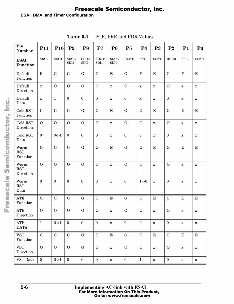
5.1.6 Port Control, Direction and Data Registers
PCR, PRR, and PDR mirror the pin functionality, direction, and state required in every task performed throughout the application. All the combinations used are condensed in
Table 5-1
. In this table,
G
stands for GPIO,
E
for ESAI,
O
for output,
x
for
donÕt care
, and
VST
for Vendor-Specific Test.
11 10 9 8 7 6 5 4 3 2 1 0
ALC TEBE SYN OF2 OF1 OF0
0 0 0 0 0 0 0 0 0 0 0 0
23 22 21 20 19 18 17 16 15 14 13 12
0 0 0 0 0 0 0 0 0 0 0 0
AA1571
Fre
esc
ale
Se
mic
on
du
cto
r, I
Freescale Semiconductor, Inc.
For More Information On This Product, Go to: www.freescale.com
nc
...
5-6
Implementing AC-link with ESAI
ESAI, DMA, and Timer Configuration
Table 5-1
PCR, PRR and PDR Values
Pin Number
P11 P10 P9 P8 P7 P6 P5 P4 P3 P2 P1 P0
ESAI Function
SDO0 SDO1 SDO2/SDI3
SDO3/SDI2
SDO4/SDI1
SDO5/SDI0
HCKT FST SCKT HCKR FSR SCKR
DefaultFunction
E G G G G E G E E G E E
DefaultDirection
x O O O O x O x x O x x
DefaultData
x 1 0 0 0 x 0 x x 0 x x
Cold RST Function
G G G G G E G G E G E E
Cold RSTDirection
O O O O O x O O x O x x
Cold RSTData
0 0->1 0 0 0 x 0 0 x 0 x x
Warm RST Function
G G G G G E G G E G E E
Warm RSTDirection
O O O O O x O O x O x x
Warm RSTData
0 0 0 0 0 x 0 1->0 x 0 x x
ATE Function
G G G G G E G G E G E E
ATE Direction
O O O O O x O O x O x x
ATE DATA
1 0->1 0 0 0 x 0 0 x 0 x x
VST Function
G G G G G E G G E G E E
VST Direction
O O O O O x O O x O x x
VST Data 0 0->1 0 0 0 x 0 1 x 0 x x
Fre
esc
ale
Se
mic
on
du
cto
r, I
Freescale Semiconductor, Inc.
For More Information On This Product, Go to: www.freescale.com
nc
...
ESAI, DMA, and Timer Configuration
Implementing AC-link with ESAI
5-7
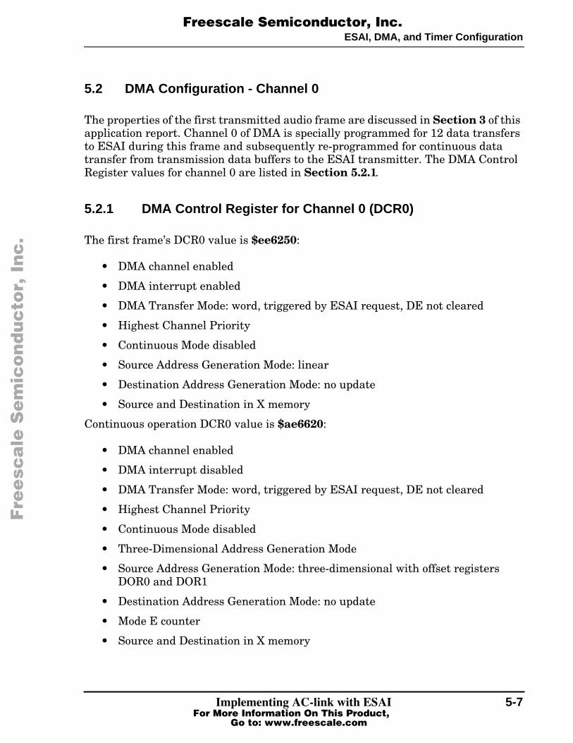
5.2 DMA Configuration - Channel 0
The properties of the first transmitted audio frame are discussed in
Section 3
of this application report. Channel 0 of DMA is specially programmed for 12 data transfers to ESAI during this frame and subsequently re-programmed for continuous data transfer from transmission data buffers to the ESAI transmitter. The DMA Control Register values for channel 0 are listed in
Section 5.2.1
.
5.2.1 DMA Control Register for Channel 0 (DCR0)
The first frameÕs DCR0 value is
$ee6250
:
¥ DMA channel enabled
¥ DMA interrupt enabled
¥ DMA Transfer Mode: word, triggered by ESAI request, DE not cleared
¥ Highest Channel Priority
¥ Continuous Mode disabled
¥ Source Address Generation Mode: linear
¥ Destination Address Generation Mode: no update
¥ Source and Destination in X memory
Continuous operation DCR0 value is
$ae6620
:
¥ DMA channel enabled
¥ DMA interrupt disabled
¥ DMA Transfer Mode: word, triggered by ESAI request, DE not cleared
¥ Highest Channel Priority
¥ Continuous Mode disabled
¥ Three-Dimensional Address Generation Mode
¥ Source Address Generation Mode: three-dimensional with offset registers DOR0 and DOR1
¥ Destination Address Generation Mode: no update
¥ Mode E counter
¥ Source and Destination in X memory
Fre
esc
ale
Se
mic
on
du
cto
r, I
Freescale Semiconductor, Inc.
For More Information On This Product, Go to: www.freescale.com
nc
...

5-8
Implementing AC-link with ESAI
ESAI, DMA, and Timer Configuration
5.2.2 DMA Counter Register for Channel 0 (DCO0)
For the first frame, the counter is initialized with $B, corresponding to 12 transfers minus one. Subsequently, the counter is re-programmed for 2 times 13 transfers, repeated circularly.
5.2.3 DMA Offset Registers (DOR0 and DOR1)
DOR0 and DOR1 are initialized with adequate values in order to swap from buffer OB0 to buffer OB1 and back to buffer OB0 in a circular way defined by DCR0 and DCO0.
5.2.4 DMA Source Address Register for Channel 0 (DSR0)
DSR0 points at any time to the current word being transferred by DMA. It is initialized with the base address of the active buffer.
5.2.5 DMA Destination Address Register for Channel 0 (DDR0)
DDR0 is programmed as the ESAI Transmit Data Register for transmitter #0 (TX0) and remains unchanged.
5.3 DMA Configuration - Channel 1
Channel 1 is programmed from the beginning for continuous data transfer from the ESAI receiver to reception data buffers. The DMA Control Register values for channel 1 are listed in
Section 5.3.1
.
5.3.1 DMA Control Register for Channel 1 (DCR1)
Continuous operation DCR1 value is
$ae5e64
:
¥ DMA channel enabled
¥ DMA interrupt disabled
¥ DMA Transfer Mode: word, triggered by ESAI request, DE not cleared
¥ Highest Channel Priority
¥ Continuous Mode disabled
Fre
esc
ale
Se
mic
on
du
cto
r, I
Freescale Semiconductor, Inc.
For More Information On This Product, Go to: www.freescale.com
nc
...

ESAI, DMA, and Timer Configuration
Implementing AC-link with ESAI
5-9
¥ Three-Dimensional Address Generation Mode
¥ Source Address Generation Mode: no update
¥ Destination Address Generation Mode: three-dimensional with offset registers DOR2 and DOR3
¥ Mode E counter
¥ Source in X memory and Destination in Y memory
5.3.2 DMA Counter Register for Channel 1(DCO1)
This register is programmed in the same way as DCO0.
5.3.3 DMA Offset Registers (DOR2 and DOR3)
DOR2 and DOR3 are initialized with adequate values in order to swap from buffer IB0 to buffer IB1 and back to buffer IB0 in a circular way defined by DCR1 and DCO1.
5.3.4 DMA Source Address Register for Channel 1(DSR1)
DSR1 is programmed as the ESAI Receive Data Register for receiver #0 (RX0) and remains unchanged.
5.3.5 DMA Destination Address Register for Channel 1 (DDR1)
DDR1 points at any time to the current word being transferred by DMA. It is initialized with the base address of the first active buffer.
5.4 Timer Configuration
The timer module is used for pulse generation on AC-link reset and test signalling. It is programmed only to count the number of internal clock cycles corresponding to the desired pulse duration.
Fre
esc
ale
Se
mic
on
du
cto
r, I
Freescale Semiconductor, Inc.
For More Information On This Product, Go to: www.freescale.com
nc
...

5-10
Implementing AC-link with ESAI
ESAI, DMA, and Timer Configuration
5.4.1 Timer Control/Status Register (TCSR)
For all pulse generation routines, TCSR is programmed with the same value:
$4
. This corresponds to:
¥ Timer Compare Interrupt enabled
¥ Timer Mode with internal Clock
5.4.2 Timer Load Register (TLR)
The timer counter is cleared before timer enabling, by writing
$0
to TLR.
5.4.3 Timer Compare Register (TCPR)
TCPR is programmed with a clock cycles count corresponding to the desired pulse.
Fre
esc
ale
Se
mic
on
du
cto
r, I
Freescale Semiconductor, Inc.
For More Information On This Product, Go to: www.freescale.com
nc
...

Code and Equates
Implementing AC-link with ESAI
Appendix A-1
Appendix A Code and Equates
This Appendix presents the assembly code and defined equates for this application.
A.1 Data Memory Usage
The following tables describe the use of X and Y data memory space. The FIFO sizes are for illustration only and do not reflect any specific application.
Table A-1
Data X-Memory Usage
$Address x Description
000 - 00C OB0 TX buffer
010 - 017 OPCM_FIFO output pcm FIFO
018 - 02f OCMD_FIFO output control FIFO
020 - 027 OMDM_FIFO output modem line FIFO
028 - 01f IPCM_FIFO input pcm FIFO
030 - 037 ISTAT_FIFO input status FIFO
038 - 03f IMDM_FIFO input modem line FIFO
040 -047 IMIC_FIFO input microphone FIFO
...
070 - 074 OIFIFO_ORDER schedule of output FIFOs
080 - 085 IFIFO_ORDER schedule of input FIFOs
090 - 095 ISTAT entries
FIFO Tables
098 - 09D IPCM entries
0A0 - 0A5 IMDM entries
0A8 - 0AD IMIC entries
0B0 - 0B5 OCMD entries
0B8 - 0BD OPCM entries
0C0 - 0C5 OMDM entries
Fre
esc
ale
Se
mic
on
du
cto
r, I
Freescale Semiconductor, Inc.
For More Information On This Product, Go to: www.freescale.com
nc
...

Appendix A-2
Implementing AC-link with ESAI
Code and Equates
A.2 Equates
As part of the respective DSP56300 derivative I/O and Interrupt Equates, the AC-link application assembly code uses the equates defined in the following paragraphs.
AC-link table
0F0 PDR_AFTER_RST PDR value after called reset
100 - 10C OB1 TX buffer
Table A-2
Data Y-Memory Usage
$Address Y Description
000 - 00C IB0 RX buffer
100 - 10C IB1 RX buffer
Table A-3
FIFO Table, Initial Status
FIFO Begin of FIFO
End of FIFO
Size of FIFO
Current READ Pointer
Current WRITE Pointer
FLAGS String
ISTAT $30 $37 $7 $30 $30 $2
IPCM $28 $2F $7 $28 $28 $2
IMDM $38 $3F $7 $38 $38 $2
IMIC $40 $47 $7 $40 $40 $2
OCMD $18 $1F $7 $18 $18 $2
OPCM $10 $17 $7 $10 $10 $2
OMDM $20 $27 $7 $20 $20 $2
Table A-1
Data X-Memory Usage (Continued)
$Address x Description
Fre
esc
ale
Se
mic
on
du
cto
r, I
Freescale Semiconductor, Inc.
For More Information On This Product, Go to: www.freescale.com
nc
...

Code and Equates
Implementing AC-link with ESAI
Appendix A-3
A.2.1 General Equates
;------------------------------------------------------------------------; AC-LINK APPLICATION EQUATES ;------------------------------------------------------------------------; General;------------------------------------------------------------------------START equ $100 ; Main Program Starting AddressTOGGLE_MODULE equ $1ff ; Module Addressing Factor for Active
; Buffer Toggling
A.2.2 ESAI Configuration Equates
;------------------------------------------------------------------------; ESAI;------------------------------------------------------------------------TCR_INIT equ $010f00 ; Initial Value for TCR RCR_INIT equ $810f00 ; Initial Value for RCR TCCR_INIT equ $441800 ; Initial Value for TCCR RCCR_INIT equ $001800 ; Initial Value for RCCR SAICR_INIT equ $000000 ; Initial Value for SAICRPRR_INIT equ $000fff ; Initial Value for PRR (reset)PCR_INIT equ $00000 ; Initial Value for PCR (reset)PDR_INIT equ $00000 ; Initial Value for PDR (reset);------------------------------------------------------------------------TCR_ACT equ $010f01 ; ESAI Enabling Value for TCRRCR_ACT equ $810f01 ; ESAI Enabling Value for RCRPDR_ACT equ $00400 ; ESAI Enabling Value for PDRPCR_ACT equ $00085b ; ESAI Enabling Value for PCR
A.2.3 DMA Programming Equates
;------------------------------------------------------------------------; DMA;------------------------------------------------------------------------DMA0_COUNT_F0 equ $b ; First Audio Frame DMA Channel #0
; CounterDMA_COUNT equ $00100c ; DMA counter prog: 2 * 13 wordsDMA_OFFSET_0 equ $f4 ; DOR0 Value DMA_OFFSET_1 equ $fffef4 ; DOR1 ValueDMA_OFFSET_2 equ $fffef4 ; DOR2 ValueDMA_OFFSET_3 equ $f4 ; DOR3 Value DMA_0_CTRL_F0 equ $ee6250 ; DMA configuration for channel 0, First
; FrameDMA_0_CTRL equ $ae6620 ; DMA configuration for channel 0DMA_1_CTRL equ $ae5e64 ; DMA configuration for channel 1
Fre
esc
ale
Se
mic
on
du
cto
r, I
Freescale Semiconductor, Inc.
For More Information On This Product, Go to: www.freescale.com
nc
...

Appendix A-4
Implementing AC-link with ESAI
Code and Equates
A.2.4 Timer Programming Equates
;------------------------------------------------------------------------; TIMER;------------------------------------------------------------------------TCSR1_RST equ $000004TCSR1_RST_ENABLE equ $000005
A.2.5 Data Structure Equates
;------------------------------------------------------------------------; AC-LINK SLOTS;------------------------------------------------------------------------SLOT_1_MASK equ $c00000SLOT_2_MASK equ $a00000SLOT_3_MASK equ $900000SLOT_4_MASK equ $880000SLOT_5_MASK equ $840000;------------------------------------------------------------------------; BUFFERS;------------------------------------------------------------------------DATA_B0 equ $0 ; First Data Buffer Base Address DATA_B1 equ $100 ; Second Data Buffer Base Address;------------------------------------------------------------------------; FIFOs;------------------------------------------------------------------------AC_LINK_TABLE equ $f0;--------------------------------------------------------------------------; FIFOs SCHEDULE;------------------------------------------------------------------------OFIFOS_ORDER equ $70IFIFOS_ORDER equ $80;--------------------------------------------------------------------------; FIFOs TABLE;------------------------------------------------------------------------FIFOS_TABLE equ $90;columnsFIFO_BEG equ $0FIFO_END equ $1FIFO_SIZE equ $2FIFO_RD equ $3FIFO_WR equ $4FIFO_FGS equ $5;flagsFULL_FG equ $0EMPTY_FG equ $1
;--------------------------------------------------------------------------; Output FIFOs
Fre
esc
ale
Se
mic
on
du
cto
r, I
Freescale Semiconductor, Inc.
For More Information On This Product, Go to: www.freescale.com
nc
...

Code and Equates
Implementing AC-link with ESAI
Appendix A-5
;------------------------------------------------------------------------OPCM_FIFO_BEG equ $010OPCM_FIFO_END equ $017OPCM_FIFO_SIZE equ (OPCM_FIFO_END-OPCM_FIFO_BEG) ; size -1 ;--------------------------------------------------------------------------OCMD_FIFO_BEG equ $018OCMD_FIFO_END equ $01fOCMD_FIFO_SIZE equ (OCMD_FIFO_END-OCMD_FIFO_BEG) ; size -1 ;--------------------------------------------------------------------------OMDM_FIFO_BEG equ $020OMDM_FIFO_END equ $027OMDM_FIFO_SIZE equ (OMDM_FIFO_END-OMDM_FIFO_BEG) ; size -1 ;--------------------------------------------------------------------------; Input FIFOs;------------------------------------------------------------------------IPCM_FIFO_BEG equ $028IPCM_FIFO_END equ $02fIPCM_FIFO_SIZE equ (IPCM_FIFO_END-IPCM_FIFO_BEG) ; size -1 ;--------------------------------------------------------------------------ISTAT_FIFO_BEG equ $030ISTAT_FIFO_END equ $037ISTAT_FIFO_SIZE equ (ISTAT_FIFO_END-ISTAT_FIFO_BEG) ; size -1 ;--------------------------------------------------------------------------IMDM_FIFO_BEG equ $038IMDM_FIFO_END equ $03fIMDM_FIFO_SIZE equ (IMDM_FIFO_END-IMDM_FIFO_BEG) ; size -1 ;--------------------------------------------------------------------------IMIC_FIFO_BEG equ $040IMIC_FIFO_END equ $047IMIC_FIFO_SIZE equ (IMIC_FIFO_END-IMIC_FIFO_BEG) ; size -1
A.2.6 AC-link Reset Routines Equates
;------------------------------------------------------------------------; RESET;------------------------------------------------------------------------CR_COUNT equ $0001B8 ; Timer Counter Value for Cold ResetWR_COUNT equ 260 ; Timer Counter Value for Warm ResetPCR_COLD_RST equ $00004bPDR_COLD_RST equ $000000PCR_WARM_RST equ $00084bPDR_WARM_RST equ $000010PDR_AFTER_RST equ (AC_LINK_TABLE)PDR_AFTER_COLD equ $000400 ; esai/gpio pins data (reset exit)PDR_AFTER_WARM equ $000000 ; esai/gpio pins data (reset exit) PCR_AFTER_RST equ $00085b ; esai pin configuration (reset exit)
Fre
esc
ale
Se
mic
on
du
cto
r, I
Freescale Semiconductor, Inc.
For More Information On This Product, Go to: www.freescale.com
nc
...

Appendix A-6
Implementing AC-link with ESAI
Code and Equates
A.2.7 AC-link Test Routines Equates
;------------------------------------------------------------------------; TEST;------------------------------------------------------------------------PDR_ATE equ $000800 ; esai/gpio pins data for ATE transition
; (SDATA_OUT high)PDR_AFTER_ATE equ $000c00 ; esai/gpio pins data (reset exit)PDR_VST equ $000010 ; esai/gpio pins data for VST transition
; (SYNC high)PDR_AFTER_VST equ $000410 ; esai/gpio pins data (reset exit)
A.3 Main Code Routines
A.3.1 Initial Procedure
org P:STARTinitial
move #DATA_B0,r7 ; not-active active buffer core; pointer
clr amove #TOGGLE_MODULE,m7move #(DATA_B1-DATA_B0),n7 ; buffer size for module add.
; updatingmovep #$0,x:M_BCR ; no wait statesmovep #$000303,x:M_IPRP ; set ESSI0 and TIMER priority to
; 2movep #$00F000,x:M_IPRC ; set DMA priority to 2move #$0,sr ; DSP interrupt
; priority=0-->enable int.move a,x:(r7) ; Audio Frame Not-validmove a,x:(r7+n) ; Audio Frame Not-valid
A.3.2 ESAI Configuration
esai_progmovep #TCR_INIT,x:M_TCRmovep #RCR_INIT,x:M_RCRmovep #TCCR_INIT,x:M_TCCRmovep #RCCR_INIT,x:M_RCCRmovep #SAICR_INIT,x:M_SAICRmovep #PRR_INIT,x:M_PRR movep #PCR_INIT,x:M_PCRmovep #PDR_INIT,x:M_PDR
Fre
esc
ale
Se
mic
on
du
cto
r, I
Freescale Semiconductor, Inc.
For More Information On This Product, Go to: www.freescale.com
nc
...

Code and Equates
Implementing AC-link with ESAI
Appendix A-7
A.3.3 DMA Programming
dma_progmovep #(DATA_B1+1),x:M_DSR0movep #DMA_OFFSET_0,x:M_DOR0movep #DMA_OFFSET_1,x:M_DOR1movep #M_TX0,x:M_DDR0movep #DMA0_COUNT_F0,x:M_DCO0
movep #M_RX0,x:M_DSR1movep #(DATA_B1),x:M_DDR1movep #DMA_COUNT,x:M_DCO1movep #DMA_OFFSET_2,x:M_DOR2movep #DMA_OFFSET_3,x:M_DOR3
A.3.4 DMA Activation
activate_dmamovep #DMA_0_CTRL_F0,x:M_DCR0movep #DMA_1_CTRL,x:M_DCR1
A.3.5 ESAI Activation
activate_esaimovep #$000000,x:M_TX0 ; First data to Transmitter, ZERO, since
; Frame is not validmovep #PDR_ACT,x:M_PDR movep #PCR_ACT,x:M_PCRmovep #TCR_ACT,x:M_TCRmovep #RCR_ACT,x:M_RCR
A.4 AC_link Test Routines
A.4.1 ATE
ate_testmove #PDR_AFTER_ATE,amove a,x:PDR_AFTER_RSTmovep #$0,x:M_TLR1 ; zero timer load register movep #CR_COUNT,x:M_TCPR1 ; count #COUNT timer clocksmovep #TCSR1_RST,x:M_TCSR1 ; program timermovep #PCR_COLD_RST,x:M_PCRmovep #PDR_ATE,x:M_PDRmovep #TCSR1_RST_ENABLE,x:M_TCSR1 ; enable timerrts
Fre
esc
ale
Se
mic
on
du
cto
r, I
Freescale Semiconductor, Inc.
For More Information On This Product, Go to: www.freescale.com
nc
...
Appendix A-8
Implementing AC-link with ESAI
Code and Equates
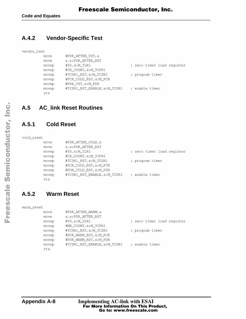
A.4.2 Vendor-Specific Test
vendor_testmove #PDR_AFTER_VST,amove a,x:PDR_AFTER_RSTmovep #$0,x:M_TLR1 ; zero timer load register movep #CR_COUNT,x:M_TCPR1movep #TCSR1_RST,x:M_TCSR1 ; program timermovep #PCR_COLD_RST,x:M_PCRmovep #PDR_VST,x:M_PDRmovep #TCSR1_RST_ENABLE,x:M_TCSR1 ; enable timerrts
A.5 AC_link Reset Routines
A.5.1 Cold Reset
cold_resetmove #PDR_AFTER_COLD,amove a,x:PDR_AFTER_RSTmovep #$0,x:M_TLR1 ; zero timer load register movep #CR_COUNT,x:M_TCPR1movep #TCSR1_RST,x:M_TCSR1 ; program timermovep #PCR_COLD_RST,x:M_PCRmovep #PDR_COLD_RST,x:M_PDRmovep #TCSR1_RST_ENABLE,x:M_TCSR1 ; enable timerrts
A.5.2 Warm Reset
warm_resetmove #PDR_AFTER_WARM,amove a,x:PDR_AFTER_RSTmovep #$0,x:M_TLR1 ; zero timer load register movep #WR_COUNT,x:M_TCPR1movep #TCSR1_RST,x:M_TCSR1 ; program timermovep #PCR_WARM_RST,x:M_PCRmovep #PDR_WARM_RST,x:M_PDRmovep #TCSR1_RST_ENABLE,x:M_TCSR1 ; enable timerrts
Fre
esc
ale
Se
mic
on
du
cto
r, I
Freescale Semiconductor, Inc.
For More Information On This Product, Go to: www.freescale.com
nc
...

Code and Equates
Implementing AC-link with ESAI
Appendix A-9
A.6 Interrupt Routines
A.6.1 Timer Interrupt
timer_1movep x:PDR_AFTER_RST,x:M_PDR ; pulse conclusionmovep #PCR_AFTER_RST,x:M_PCR ; enble ESAI with new
; configurationrti
A.6.2 DMA Channel #0 Interrupt
dma_0bclr #23,x:M_DCR0 ; disable DMAmovep #DMA_COUNT,x:M_DCO0 ; number of wordsmovep #DATA_B0,X:M_DSR0movep #DMA_0_CTRL,x:M_DCR0 ; enable DMA, this time with
; interrupt disabledrti
A.6.3 ESAI Receive Last Slot Interrupt
rx_last_slot_intmove (r7)+n ; toggle B0<->B1, r7move #OFIFOS_ORDER,r2 ; point to FIFOs’ scehdulemove #FIFO_FGS,n3 ; point to FLAGS columnmove r7,x0 ; save r7clr a (r7)+ ; clear TAG, point R7 to next
; data slotdo #$5,end_rx_last_slot_int_readmove x:(r2)+,r3 ; point to current FIFOs' rowmove x:(r2)+,y1 ; get fifos' maskjset #EMPTY_FG,x:(r3+n),eend_rx_last_slot_int_read
; read from fifo; unless it's EMPTY
move x:(r3+FIFO_RD),r1 ; get read pointer move x:(r3+FIFO_SIZE),m1 ; get FIFO’s size for module
; addressing move x:(r1)+,x1 ; read from FIFObclr #FULL_FG,x:(r3+n) ; clear FULL flagmove x1,x:(r7) ; write to buffermove r1,x:(r3+FIFO_RD) ; update RD pointeror y1,a ; update tag move x:(r3+FIFO_WR),b ; get write pointermove r1,x1cmp x1,b
Fre
esc
ale
Se
mic
on
du
cto
r, I
Freescale Semiconductor, Inc.
For More Information On This Product, Go to: www.freescale.com
nc
...

Appendix A-10
Implementing AC-link with ESAI
Code and Equates
jne eend_rx_last_slot_int_read ; set EMPTY flag in case RD=WRbset #EMPTY_FG,x:(r3+n)
eend_rx_last_slot_int_readmove (r7)+ ; point R7 to next data slotnopnopnopnop
end_rx_last_slot_int_read;--------------------------------------------------------------------------
move x0,r7 ; recover r7 move a1,x:(r7) ; update TAG
;--------------------------------------------------------------------------move #IFIFOS_ORDER,r2 ; point to FIFOs’ schedulemove y:(r7)+,a ; get input buffer's TAGlsl ajcc end_rx_last_slot_int_write ; end in case this frame is NOT
; VALIDdo #$6,end_rx_last_slot_int_writemove x:(r2)+,r3 ; point to current FIFOs’ tablejset #FULL_FG,x:(r3+n),crash ; write to FIFO unless it's FULLlsl ajcc eend_rx_last_slot_int_write ; end in case this slot is NOT
; VALIDmove x:(r3+FIFO_WR),r1 ; get write pointer move x:(r3+FIFO_SIZE),m1 ; get FIFO’s size for module
; addressing move y:(r7),x1 ; read bufferbclr #EMPTY_FG,x:(r3+n) ; clear EMPTY flagmove x1,x:(r1)+ ; write to FIFOmove r1,x:(r3+FIFO_WR) ; update WR pointermove x:(r3+FIFO_RD),b ; get read pointermove r1,x1cmp x1,bjne eend_rx_last_slot_int_write ; set FULL flag in case RD=WRbset #FULL_FG,x:(r3+n)
eend_rx_last_slot_int_writemove (r7)+ ; point R7 to next data slotnopnopnopnopnopnop
end_rx_last_slot_int_writemove x0,r7 ; recover r7nopnopnopnoprti
Fre
esc
ale
Se
mic
on
du
cto
r, I
Freescale Semiconductor, Inc.
For More Information On This Product, Go to: www.freescale.com
nc
...

Code and Equates
Implementing AC-link with ESAI
Appendix A-11
A.7 Crash Routine
The AC-link application enters a
crash
routine when it tries to write to any input FIFO that is full. The Audio application should handle this situation and define the applicable procedureÑfor example, immediately processing the FIFO contents or enlarging the FIFO capacity.
Fre
esc
ale
Se
mic
on
du
cto
r, I
Freescale Semiconductor, Inc.
For More Information On This Product, Go to: www.freescale.com
nc
...

Appendix A-12
Implementing AC-link with ESAI
Code and Equates
Fre
esc
ale
Se
mic
on
du
cto
r, I
Freescale Semiconductor, Inc.
For More Information On This Product, Go to: www.freescale.com
nc
...

Implementing AC-link with ESAI
Appendix B-1
Appendix B References
The following manuals, which may contain data pertinent to this application, may be viewed or downloaded at the indicated web sites.
¥ http://www.mot.com/SPS/DSP/documentation/DSP56300.html
DSP56300 Digital Signal Processor Family Manual
DSP56362 Digital Signal Processor User's Manual
DSP56362 Digital Signal Processor Data Sheet
DSP56300 Digital Signal Processor Family: DMA Application Note
Application Optimization Note for the DSP56300/DSP56600 Family
¥ http://developer.intel.com/pc-supp/platform/ac97
Audio Codec `97 Component Specification
. Revision 1.03 (September 1996) and 2.0 (September 1997). Primary Developers: Analog Devices. Creative Labs, Inc. Intel Corporation. National Semiconductor Yamaha Corporation. Copyright 1997, Intel Corporation.
Fre
esc
ale
Se
mic
on
du
cto
r, I
Freescale Semiconductor, Inc.
For More Information On This Product, Go to: www.freescale.com
nc
...

Appendix B-2
Implementing AC-link with ESAI
Fre
esc
ale
Se
mic
on
du
cto
r, I
Freescale Semiconductor, Inc.
For More Information On This Product, Go to: www.freescale.com
nc
...

Implementing AC-link with ESAI
NOTES:
Fre
esc
ale
Se
mic
on
du
cto
r, I
Freescale Semiconductor, Inc.
For More Information On This Product, Go to: www.freescale.com
nc
...

Implementing AC-link with ESAI
NOTES:
Fre
esc
ale
Se
mic
on
du
cto
r, I
Freescale Semiconductor, Inc.
For More Information On This Product, Go to: www.freescale.com
nc
...

Order by this number:
APR37/D
Fre
esc
ale
Se
mic
on
du
cto
r, I
Freescale Semiconductor, Inc.
For More Information On This Product, Go to: www.freescale.com
nc
...

Fre
esc
ale
Se
mic
on
du
cto
r, I
Freescale Semiconductor, Inc.
For More Information On This Product, Go to: www.freescale.com
nc
...