implicit mixed-mode simulation of vlsi circuitsgnucap.org/papers/al-davis-dissertation.pdf ·...
TRANSCRIPT

Implicit Mixed-Mode Simulationof VLSI Circuits
by
Albert Tatum Davis
Submitted in Partial Fulfillmentof the
Requirements for the Degree
Doctor of Philosophy
Supervised by Robert J. Bowman
Department of Electrical EngineeringCollege of Engineering and Applied Science
University of RochesterRochester, New York
1991

i
Curriculum Vitae
Albert Davis was born on June 29, 1950 in Albany, New York. He
graduated from Clarkson College in 1972 with a B.S. degree in Elec-
trical and Computer engineering, with a specialty in communications
and circuit theory.
From 1972 to 1978 he was employed as an analog circuit designer,
working primarily in the audio industry. In 1978, he founded Tatum
Labs, a consulting firm, to do analog circuit design. Beginning in 1980,
his work became primarily software tools for circuit designers. Tatum
Labs developed and marketed entry level CAD software, including a
circuit simulator, for board level circuits. He sold Tatum Labs in 1986
to pursue full time graduate study.
In 1984, he enrolled in a part time Masters program at the Uni-
versity of Bridgeport. He received the M.S. degree in 1986. In 1986
he enrolled in a Ph.D. program at Clarkson University. In 1987, he
transferred to the University of Rochester to complete his research un-
der Dr. Robert Bowman. His research concentrated on simulation of
mixed analog and digital circuits.

ii
Abstract
Circuit simulation is an important tool for the design and verification of inte-
grated circuits. It is increasingly common to combine analog and digital subcir-
cuits on a single chip. These combined circuits present problems for simulation.
In this dissertation some techniques are presented to combine different simulation
modes, logic and analog, implicitly, without direct instructions from the user.
This results in improved simulation of combined analog and digital circuits.
A unified data structure allows the free mixing of analog and digital devices,
with support for both analog and logic level simulation simultaneously. The ana-
log simulation is based on traditional algorithms, LU decomposition by a modified
Crout method and iteration by Newton’s method, enhanced to support incremen-
tal changes to the matrix and to bypass of parts of the matrix solution that are
inactive or already converged. The resulting simulation is much faster than the
traditional solution method with bypass only applied to model evaluation, without
loss of accuracy. The logic level simulation is based on traditional event driven
logic simulation, where logic states are propagated. A logic element has both a
circuit and logic description.
A method is presented to automatically choose between logic and analog simu-
lation in parts of the circuit that have a logic level description. The choice is based
on the assumption that when the digital signals appear to be clean a digital sim-
ulation is valid. When the digital signals show race and spike conditions or slow
transitions they are suspect and analog simulation is used for the problem parts
of the circuit. When the conversion between modes is poorly defined or difficult
to make the analog mode is selected. The simulation mode changes dynamically
as the simulation runs. Mode changes can be made on parts of the circuit as small
as a single gate.
For digital circuits these techniques are much faster than full analog simulation.
They accurately simulate cases where digital simulation fails by applying analog
techniques on a local basis and they simulate the interface between analog and
digital parts of the circuit better than other methods.

iii
Acknowledgements
I would like to thank Mike Wengler, Vassilios Tourassis, and Rob
Fowler for serving on my thesis committee. I am particularly grateful
to Rob Fowler for help with the dissertation, and VT for bringing up
the right points at committee meetings.
I thank my thesis adviser, Robert Bowman, for maintaining faith,
even when I lost it, no matter how rough things were.
I acknowledge the financial support of Siemens Corporation, and
Analog Devices Corporation. I also thank Tatum Labs for the use of
the “ECA-2” source code, to use as a base for the “URECA” simulator,
and for providing some extra income in the form of ECA-2 royalties,
so I was a little better off financially than most graduate students.
I thank Ken Ebert for buying my business (Tatum Labs) so I could
pursue graduate study, full time.
I thank Professors Gaylord Northrup and Gerry Volpe at Bridge-
port for the many fruitful conversations that inspired me to go on for
doctoral studies.
Since life is not complete without recreation, I thank the Rochester
Bicycling Club, especially Ann Carroll and Jean Jaslow, for helping
me maintain my sanity by providing an escape when the pressure was
too much.
Finally, I thank my parents, Albert and Marian, for everything.
Contents
1 Introduction 1
1.1 Motivation . . . . . . . . . . . . . . . . . . . . . . . . . . . . . . . 1
1.2 Research objectives . . . . . . . . . . . . . . . . . . . . . . . . . . 3
2 Background of Circuit Simulation 6
2.1 Types of Simulation . . . . . . . . . . . . . . . . . . . . . . . . . . 6
2.1.1 Classical network simulation . . . . . . . . . . . . . . . . . 6
2.1.2 Logic level simulation . . . . . . . . . . . . . . . . . . . . . 8
2.1.3 Switch level simulation . . . . . . . . . . . . . . . . . . . . 9
2.1.4 Timing simulation . . . . . . . . . . . . . . . . . . . . . . 9
2.1.5 Mixed-mode simulation . . . . . . . . . . . . . . . . . . . . 10
2.2 Classic Circuit Simulation . . . . . . . . . . . . . . . . . . . . . . 11
2.2.1 DC analysis . . . . . . . . . . . . . . . . . . . . . . . . . . 11
2.2.2 Transient analysis . . . . . . . . . . . . . . . . . . . . . . . 18
2.2.3 Logic simulation . . . . . . . . . . . . . . . . . . . . . . . 22
2.3 Related Works in Simulation . . . . . . . . . . . . . . . . . . . . . 26
2.3.1 MOTIS . . . . . . . . . . . . . . . . . . . . . . . . . . . . 26
iv

CONTENTS v
2.3.2 DIANA . . . . . . . . . . . . . . . . . . . . . . . . . . . . 28
2.3.3 SPLICE . . . . . . . . . . . . . . . . . . . . . . . . . . . . 29
2.3.4 MACRO . . . . . . . . . . . . . . . . . . . . . . . . . . . . 30
2.3.5 SAMSON . . . . . . . . . . . . . . . . . . . . . . . . . . . 31
2.3.6 ADEPT . . . . . . . . . . . . . . . . . . . . . . . . . . . . 32
2.3.7 RELAX . . . . . . . . . . . . . . . . . . . . . . . . . . . . 34
2.4 Mixed Mode Simulation . . . . . . . . . . . . . . . . . . . . . . . 36
2.4.1 Event Driven Circuit Simulation: SAMSON . . . . . . . . 37
3 Implicit Mixed Mode Simulation 51
3.1 LU decomposition . . . . . . . . . . . . . . . . . . . . . . . . . . . 51
3.1.1 Review, Basics, Crout’s algorithm . . . . . . . . . . . . . . 52
3.1.2 Sparse vector method . . . . . . . . . . . . . . . . . . . . . 57
3.1.3 Solving only part of the matrix . . . . . . . . . . . . . . . 67
3.2 Iterative methods . . . . . . . . . . . . . . . . . . . . . . . . . . . 69
3.2.1 Fixed Point Iteration . . . . . . . . . . . . . . . . . . . . . 70
3.2.2 Relaxation methods . . . . . . . . . . . . . . . . . . . . . . 73
3.3 Local step control . . . . . . . . . . . . . . . . . . . . . . . . . . . 75
3.3.1 Solving part of the circuit . . . . . . . . . . . . . . . . . . 75
3.3.2 The event queue . . . . . . . . . . . . . . . . . . . . . . . 78
3.3.3 Selective trace applied to LU decomposition . . . . . . . . 79
3.4 Logic simulation . . . . . . . . . . . . . . . . . . . . . . . . . . . . 81
3.4.1 Logic States . . . . . . . . . . . . . . . . . . . . . . . . . . 82

CONTENTS vi
3.4.2 Inconsistencies . . . . . . . . . . . . . . . . . . . . . . . . 84
3.5 Mixed simulation . . . . . . . . . . . . . . . . . . . . . . . . . . . 88
3.5.1 Data Structures . . . . . . . . . . . . . . . . . . . . . . . . 88
3.5.2 Choice of methods, how? . . . . . . . . . . . . . . . . . . . 91
3.5.3 Circuit to Logic Conversion . . . . . . . . . . . . . . . . . 92
3.5.4 Logic to Circuit Conversion . . . . . . . . . . . . . . . . . 94
4 Results 98
4.1 The URECA Simulator . . . . . . . . . . . . . . . . . . . . . . . . 98
4.2 Sparse matrix: A Large Linear Circuit . . . . . . . . . . . . . . . 102
4.3 Incremental update: A Comparator . . . . . . . . . . . . . . . . . 105
4.4 Mixed-mode simulation: A string of gates . . . . . . . . . . . . . 107
4.4.1 Clean Digital Input . . . . . . . . . . . . . . . . . . . . . . 111
4.4.2 A Signal Too Slow . . . . . . . . . . . . . . . . . . . . . . 112
4.4.3 Input Signal Too Small . . . . . . . . . . . . . . . . . . . . 120
4.4.4 Summary . . . . . . . . . . . . . . . . . . . . . . . . . . . 122
5 Contributions and Research Suggestions 123
5 Bibliography 130

List of Figures
2.1 A simple circuit . . . . . . . . . . . . . . . . . . . . . . . . . . . 12
2.2 Companion models for the Backward Euler formula . . . . . . . . 19
2.3 Logic to circuit signal conversion . . . . . . . . . . . . . . . . . . 45
2.4 A rising circuit switching signal (smooth) . . . . . . . . . . . . . 45
2.5 A piece-wise linear rising waveform . . . . . . . . . . . . . . . . . 46
2.6 Simplified model of a logic subnet . . . . . . . . . . . . . . . . . 46
2.7 Temporally overlapping transitions . . . . . . . . . . . . . . . . . 47
2.8 Multiple overlapping transitions . . . . . . . . . . . . . . . . . . 47
2.9 Thresholding . . . . . . . . . . . . . . . . . . . . . . . . . . . . . 48
2.10 Improper logic signal produced by thresholding . . . . . . . . . . 49
2.11 Correct response to improper logic signal . . . . . . . . . . . . . 49
3.1 Crout’s algorithm . . . . . . . . . . . . . . . . . . . . . . . . . . . 54
3.2 Crout’s algorithm on a banded with spikes sparse matrix . . . . . 55
3.3 Crout’s algorithm on a BBD matrix . . . . . . . . . . . . . . . . . 56
3.4 Modified Crout’s algorithm . . . . . . . . . . . . . . . . . . . . . . 62
3.5 Modified Crout’s algorithm on a banded with spikes sparse matrix 65
vii

LIST OF FIGURES viii
3.6 Modified Crout’s algorithm on a BBD matrix . . . . . . . . . . . 66
3.7 Distinct transitions . . . . . . . . . . . . . . . . . . . . . . . . . . 84
3.8 Overlapping transitions . . . . . . . . . . . . . . . . . . . . . . . 85
3.9 Overlapping transitions, no spike . . . . . . . . . . . . . . . . . . 86
3.10 Thresholding . . . . . . . . . . . . . . . . . . . . . . . . . . . . . 93
3.11 Improper logic signal produced by thresholding . . . . . . . . . . 93
3.12 Logic to circuit signal conversion . . . . . . . . . . . . . . . . . . 96
4.1 A 10 band graphic equalizer . . . . . . . . . . . . . . . . . . . . . 102
4.2 Many equalizers . . . . . . . . . . . . . . . . . . . . . . . . . . . . 103
4.3 A comparator circuit . . . . . . . . . . . . . . . . . . . . . . . . . 106
4.4 A string of inverters . . . . . . . . . . . . . . . . . . . . . . . . . 108
4.5 A CMOS inverter . . . . . . . . . . . . . . . . . . . . . . . . . . . 108
4.6 Logic display syntax . . . . . . . . . . . . . . . . . . . . . . . . . 109

List of Algorithms
2.1 Linear DC Analysis . . . . . . . . . . . . . . . . . . . . . . . . . 12
2.2 Nonlinear DC Analysis . . . . . . . . . . . . . . . . . . . . . . . 17
2.3 Non-Event Driven Logic Simulation . . . . . . . . . . . . . . . . 23
2.4 Event Driven Logic Simulation . . . . . . . . . . . . . . . . . . . 25
2.5 MOTIS algorithm . . . . . . . . . . . . . . . . . . . . . . . . . . 27
2.6 Event Driven Circuit Simulation . . . . . . . . . . . . . . . . . . 41
2.7 Event Driven Logic Simulation . . . . . . . . . . . . . . . . . . . 44
3.1 Crout’s algorithm . . . . . . . . . . . . . . . . . . . . . . . . . . 53
3.2 Forward Substitution . . . . . . . . . . . . . . . . . . . . . . . . 53
3.3 Backward Substitution . . . . . . . . . . . . . . . . . . . . . . . . 53
3.4 Modified Crout Algorithm . . . . . . . . . . . . . . . . . . . . . . 63
3.5 Modified Crout with Zero Bypass . . . . . . . . . . . . . . . . . . 64
3.6 Relaxation: Jacobi Method . . . . . . . . . . . . . . . . . . . . . 74
3.7 Simulation with Jacobian Bypass . . . . . . . . . . . . . . . . . . 77
3.8 Selective Trace Applied to LU Decomposition . . . . . . . . . . . 80
3.9 Gate Evaluation . . . . . . . . . . . . . . . . . . . . . . . . . . . 83
ix

LIST OF TABLES x
3.10 Gate Evaluation, Allowing for Races . . . . . . . . . . . . . . . . 87
3.11 Circuit to Logic Conversion . . . . . . . . . . . . . . . . . . . . . 95

Chapter 1
Introduction
1.1 Motivation
As technology improves, integrated circuits grow in size and complexity. Such
circuit complexity precludes the use of breadboarding for prototyping, and de-
mands computer-assisted analysis offered by simulation. The size and complexity
of circuits has grown to the point where, often, circuit simulation has become the
major cost in the development cycle. In many cases, however, a simulation does
not produce satisfactory results. Changes to the circuit description are required to
get the simulator to run. Often, the resulting model or topology may no longer be
an accurate representation of the actual circuit. A circuit may often be simulated
successfully by partitioning into smaller blocks and applying different algorithms
to different blocks. Reconnecting the blocks together often causes interactions
that separate simulations do not show.
Considerable progress in simulation has been made for digital circuits, and for
1

1.1. MOTIVATION 2
many classes of analog circuits. However, there are classes of circuits, particularly
in the analog domain, that continue to plague simulation tools with problems of
convergence and accuracy. These circuits are characterized by widely varying time
constants, and often include mixed analog and digital blocks with feedback. They
can be small or large. The number of active elements ranges from 5 to 100,000
devices. Examples of the problem circuits include A/D converters, phase locked
loops, switched capacitor circuits, and oscillator start-up circuits.
A new generation of mixed-mode simulators has evolved to apply different
algorithms to different blocks. However, the burden of selecting the most ap-
propriate algorithm for each block rests with the designer. The netlist accepts
both circuit and logic level elements, with some restrictions on how they connect
together. Some require entire subcircuit blocks to be all either digital or analog,
but not mixed. Existing simulators use this information to explicitly partition
the circuit into analog and digital parts, then apply the nominally appropriate
algorithm to each part, with explicit conversions at the interfaces.
At first this may seem to not be a problem, since the designer knows how
the circuit blocks should work, but too often the assumptions the designer made
do not hold. Only a more detailed simulation would show the failings of the
circuit. The information required to select the simulation algorithm is often the
very information the designer is seeking from the simulation.
Some circuits, specified on a device level, are best simulated by traditional
Newton-Raphson – LU decomposition methods. Some are best done by relaxation.

1.2. RESEARCH OBJECTIVES 3
Some are best done by a combination. Likewise, some circuits, specified in logic
level, can be accurately simulated by traditional logic level simulation. Some
require a more accurate “timing” simulation, which is the same as relaxation
based analog simulation, to properly simulate race conditions, or other improper
signals.
1.2 Research objectives
The two levels to consider in mixed-mode simulation are actually circuit and
behavioral. Behavioral modeling is simply evaluating the function performed by
a block, and using the result. Circuit level means to evaluate the components
that make up a block, and how they interact. Evaluating each component can
be either circuit level or behavioral. Signals can also be considered to be either
circuit level or behavioral. Circuit level signals can be measured using instruments.
Behavioral level signals are abstract quantities, or interpretations or circuit level
signals. With this in mind, the decision process is whether to use the concrete
(circuit level) or abstract (behavioral level).
In the behavioral level, only the apparent behavior at the terminals is consid-
ered, but this is not always good enough. Some means is necessary to determine
whether it is necessary to simulate the internal behavior of blocks, instead of
relying on their nominal behavior. Given a circuit block, the behavior is con-
sidered to be easily predicted if the voltages and currents at the interface points
meet certain constraints, over some time. It is desirable to determine this as the

1.2. RESEARCH OBJECTIVES 4
simulation runs, and dynamically switch modes locally. Assuming the behavioral
mode is logic level, various acceleration techniques are available, including the use
of an event queue to avoid computer time when there is no action. This research
investigates efficient techniques for mixing this with traditional analog simulation.
The following areas were investigated in this work. The results of this research
were incorporated into a general purpose simulator, “URECA”.
Multiple solution methods Some circuits are best solved by traditional meth-
ods (Newton-Raphson, LU decomposition, etc.) Some are best solved by
other methods, such as relaxation, harmonic balance, event driven, etc.
Three methods were chosen here: traditional (Newton’s method, LU de-
composition), relaxation, and gate level (behavioral, with discrete states).
Automatic choice of method Simulators exist that use a variety of methods.
All known simulators that can use more than one method require the user
to partition the circuit and specify what method to use where. In this work,
the choice between the three methods named above is made implicitly, for
each device, at run time. The choice of method changes as the simulation
progresses.
Heuristic shortcuts Often, it is not necessary to do all calculations, or use the
most complete model. Research was done to determine what shortcuts can
be taken, and how to make these decisions automatically.
Automatic partitioning of the circuit There are several reasons to partition

1.2. RESEARCH OBJECTIVES 5
the circuit. It may be advantageous to apply different methods to different
parts of the circuit. Varying time constants could allow more economic so-
lution if the slow parts can be simulated with a larger step size. There exist
known methods of partitioning[58], but they are slow. (Time grows super-
linearly with circuit size.) Likewise, the time needed to order the equations
(pivoting) grows superlinearly with circuit size. In this work, ordering and
partitioning is done crudely as part of subcircuit expansion, resulting in a
bordered block diagonal matrix. Partitioning is implicit. Simulation meth-
ods are applied to each device as appropriate. Partial solution of the matrix
uses a trace of how changes propagate to determine the parts to operate on.
Partitioning is implicit, and can change dynamically.
Chapter 2
Background of CircuitSimulation
2.1 Types of Simulation
This section introduces several types of simulation, with a brief overview. More
detail is available in sections 2.2 and 2.4. Descriptions of some of the programs
are in section 2.3.
2.1.1 Classical network simulation
The common conventional circuit simulators are based on a mechanization of
the methods taught as undergraduate circuit theory[57][30]. The most common
(SPICE)[31] are based on modified nodal analysis. Nodal analysis is simply the
application of Kirchoff’s current law. This results in a singular matrix if there are
ideal voltage sources, so a modified nodal analysis adds equations for the currents
in voltage sources.
6

2.1. TYPES OF SIMULATION 7
The resulting system of linear equations is solved by LU decomposition, and
forward and back substitution. Without sparse matrix techniques, the running
time for this isO(n3). Further details on this are available in any text on numerical
analysis[37][48].
Sparse matrix techniques improve this running time substantially. It has been
observed to be typically about O(n1.4) for a typical circuit in SPICE[31]. This
tends to deteriorate for large circuits. It is possible to do as good as linear time,
for some large circuits with few connections at each node[9]. Duff has published
a comprehensive summary of sparse matrix techniques[17].
Nonlinear circuits are solved by the Newton-Raphson method, with each iter-
ation solved by LU decomposition. This is also well documented in any numerical
analysis text.
For the time domain solution, the energy storage components (capacitors and
inductors) are discretized by some finite difference method. Usually, this is done
on a component by component basis, in effect replacing them with resistors and
sources. This is known as a companion model. The differential equations are then
converted to algebraic equations. These equations are solved at each time step.
This is costly, but if the circuit is linear only the right side of the equations
changes at each time. The LU decomposition need not be repeated, only the
forward and back substitution. Unfortunately, most circuits are not linear.
In summary, conventional methods usually gives good results, but at consid-

2.1. TYPES OF SIMULATION 8
erable cost in time.
2.1.2 Logic level simulation
At the other extreme, there is logic level simulation. Instead of the continuum
of levels that is available from conventional analog simulator, there are only a
finite number of states. Also, the circuit is often clocked. Most of the time the
circuit is latent, nothing is happening. One example of a logic level simulator is
TEGAS[51].
In the simple case, there are three states, 1, 0, and unknown. Typically, there
are also strengths, such as driven, weak, and charged, bringing the number of
states to nine. Transition states can be added. Including all possible transitions
brings the number of states to 27. The cost of many states often outweighs the
benefits, so many simulators compromise on nine states.
The circuit building blocks are the basic logic blocks: gates, flop-flops, coun-
ters, etc. Each of these blocks has an output that is defined for a given input,
after some delay. The signal flow is unidirectional through the blocks.
On a simple level, logic simulators cycle through the list of blocks, calculate
their outputs based on the input, and build the list of states for the next time.
Most of the time, most signals are latent. They are not changing. A selective trace
table indicates the blocks are affected by each node. Once this table exists, it is
only necessary to simulate those blocks of the circuit whose input changes, leading
to dramatic savings in time. It is now event driven. When the state at any node

2.1. TYPES OF SIMULATION 9
changes, its effect is looked up in the selective trace table, and placed in an event
queue. The simulation runs by stepping through the event queue, and simulating
those events. Each event changes the state at some nodes, which makes more
entries into the event queue. To start it, it is only necessary to schedule the initial
event. The running time is proportional to the number of events. The size of the
circuit and the desired time granularity have nothing to do with the running time,
beyond the setup time.
This type of simulation runs fast, but only for logic circuits, and it provides
only logic states as output.
2.1.3 Switch level simulation
Digital VLSI circuits use the devices mainly as switches. Switch level simulation[40]
takes this view. Every active device is modelled as a voltage controlled switch,
then a discrete simulation is done, using event driven selective trace techniques.
It is thus similar to logic level simulation.
2.1.4 Timing simulation
The most critical parameter in digital circuits is timing. (avoidance of race condi-
tions, etc.) A true logic level simulation does not have enough information to show
this. Timing simulation[40] considers gate delays and capacitances, to attempt to
show timing more accurately.
MOTIS[8][19] is an example of a timing simulator. This class of simulators
2.1. TYPES OF SIMULATION 10
makes the assumption that the circuit resembles a typical digital circuit, so it
can use most of the speed-up techniques that are commonly applied to logic level
simulation. Timing simulation discretized time in intervals smaller than the clock
cycle of the circuit being simulated.
Some so-called timing simulators are logic or switch level simulators that take
into account gate delays. Others are based on differential equations, like analog
simulators, but without iteration. They still assume that the signal propagates
only on one direction. The waveforms are often only accurate enough to determine
timing, but may not show second-order effects, such as overshoot. Some so-called
mixed-mode simulators are really timing simulators.
2.1.5 Mixed-mode simulation
Mixed-mode simulation applies more than one algorithm to the circuit. The circuit
is partitioned into parts to which each algorithm is applied. It often does not mean
mixed analog and digital, but perhaps two different levels of digital simulation,
such as logic (discrete states) and timing (some sense of voltage).
Some early mixed-mode simulators, such as DIANA[4][3] consist of two simu-
lators running concurrently. Two separate simulators, analog and digital, run in
lock-step with each other, and exchange information. Possible methods of com-
munication between them include UNIX pipes and VMS mailboxes.
There are mixed-mode simulators are not just two simulators running concur-
rently. (SAMSON[42][43], SPLICE[32][44][25]) The two modes are integrated into

2.2. CLASSIC CIRCUIT SIMULATION 11
one program, and communicate by special nodes or blocks. These simulators still
require the user to partition the circuit.
Implicit mixed-mode simulation, as described in this dissertation, allows the
free mixing of analog and digital modes.
2.2 Classic Circuit Simulation
This section is an overview of some well known simulation methods: DC analysis,
transient analysis, and gate level logic simulation. Simulators based on these meth-
ods are available commercially, and are well documented in several texts[1][30][57].
The information here should be familiar to those well versed in simulation and
computer aided design.
2.2.1 DC analysis
Basic Circuit Theory
The simplest analysis done by a circuit simulator is a linear DC analysis. Nearly all
simulators are based on a mechanization of the methods taught in undergraduate
circuit theory[55][46]. The most common are based on modified nodal analysis.
Nodal analysis is simply the application of Kirchoff’s current law. It solves for
all node voltages. Modified nodal analysis adds a few current variables, to fix
singularity problems with voltage sources.
The basic algorithm for linear DC analysis is shown in algorithm 2.1.

2.2. CLASSIC CIRCUIT SIMULATION 12
Read in the circuit description, and store, by branch.Allocate memory for sparse matrix system.For each branch {
Calculate its admittance and offset current.Add it to the admittance matrix or current vector.(This produces a system of linear equations.)
}Solve the system of equations.(This produces the voltages at all nodes.)Print or plot the selected values.
Algorithm 2.1: Linear DC Analysis
1 2
R1 R3
C1
R2
C2I0
0
Figure 2.1: A simple circuit
2.2. CLASSIC CIRCUIT SIMULATION 13
Consider the circuit in figure 2.1. In DC analysis, energy storage elements are
ignored by replacing capacitors by open circuits, and inductors by short circuits.
From basic circuit theory, the nodal equations representing this are:
(1
R1
+1
R2
)V1 −
(1
R2
)V2 = I0
−(
1
R2
)V1 +
(1
R2
+1
R3
)V2 = 0 (2.1)
In matrix form, this is:
1
R1
+1
R2
− 1
R2
− 1
R2
1
R2
+1
R3
[V1
V2
]=
[I0
0
](2.2)
In general, this system of equations can be represented as Yv = i where Y
is the nodal admittance matrix, v is the vector of unknown node voltages, and i
is the current excitation vector. This system of equations is solved for the node
voltages.
Typical Implementation
The first step of a typical implementation is to read the circuit description from
the file. A list of all circuit elements, with their nodes and values, is stored. No
evaluation takes place at this time.
After reading the circuit description file, memory is allocated for the matrix
(2.2) that represents the equations. Sparse matrix techniques are used in all but
the most primitive simulators. The allocation step scans the element list, and
2.2. CLASSIC CIRCUIT SIMULATION 14
sets up an indexing scheme for sparse matrix allocation. In the most primitive
simulators, it simply counts nodes then dimensions an array accordingly. At least
two arrays need to be set up: Y, the nodal admittance matrix and i, the current
excitation vector. The unknown voltage vector, v, will eventually replace i, so it
is not allocated separately. Sparse matrix schemes vary. SPICE uses a doubly
linked list in which each element is allocated separately[31]. URECA uses a vector
scheme that uses pointers to vectors representing partial rows and columns are
set up[9]. At this point the arrays are filled with zeros.
The next step is to fill in the actual values. The internal representation of
the netlist is scanned. Each element is evaluated and its admittance is added to
the appropriate place in the Y and i arrays. For example, a current source adds
its value to the place in i representing the first node, and subtracts it from the
place in i representing the second node, for a total of two entries. A resistor adds
its admittance (1/R) to the diagonal at each of its nodes, and subtracts it from
the off-diagonal places. A resistor of 10 ohms connecting between nodes 1 and 2
adds .1 to y1,1 and y2,2, and subtracts .1 from y1,2 and y2,1. Row and column 0
are thrown away, because node 0 is used as a reference, at which the voltage is by
definition zero. This sets up the system of equations Yv = i, which will be solved
next.
A true nodal analysis does not allow ideal voltage sources, so modified nodal
analysis(MNA)[24] is used. With true nodal analysis, voltage sources with series
resistance can be converted to current sources with shunt resistance. MNA is the
2.2. CLASSIC CIRCUIT SIMULATION 15
same as nodal analysis except that there are additional variables to represent cur-
rent through the voltage sources. Some variations on MNA exist, including nullor
methods[50], which replace multi-terminal elements with simple two terminal el-
ements: the nullator, which has current and voltage both zero, and the norator
for which they are both arbitrary. Some early simulators used the sparse tableau
approach[23] or a state variable approach[26]. For expediency, URECA uses a true
nodal analysis with the restriction that voltage sources must have resistance.
Once all elements are processed this way (assuming nodal analysis) we have
the system of n equations described above, where n is approximately the number
of nodes in the circuit. It is solved by LU decomposition followed by forward and
back substitution. In LU decomposition, the matrix Y is replaced by two matrices:
an upper triangular U and lower triangular L, such that LU = Y. Forward and
back substitution replaces i with the voltage (solution) vector v.
With dense matrix techniques the running time for this would be O(n3), where
n is the number of equations. Sparse matrix techniques improve this running time
substantially. For a typical circuit, it has been observed to be about O(n1.4) in
SPICE[31]. There is more detail on matrix solution methods, especially as they
apply to mixed-mode simulation, in 3.1.
At this point any information requested by the user can be printed out or sent
to a post-processor. Node voltages are available directly. Other information, such
as branch voltages and currents, can be calculated from the node voltages.

2.2. CLASSIC CIRCUIT SIMULATION 16
Nonlinear circuits
If there are nonlinear elements an iterative method is used to find the solution.
In URECA and SPICE the Newton-Raphson method is used. For the scalar case,
the current value (at iteration k) can be represented by the formula:
xk = xk−1 − f(xk−1)/f(xk−1) k = 1, 2, . . . (2.3)
For convenience, we can rearrange it as:
f(xk−1)xk = f(xk−1)xk−1 − f(xk−1) k = 1, 2, . . . (2.4)
For several variables this becomes, in matrix notation:
Ax(k) = Ax(k−1) − f(x(k−1)) k = 1, 2, . . . (2.5)
where A is the Jacobian matrix, containing the partial derivatives aij = ∂fi(x)/∂xj
for i, j = 1, . . . , n. This results in a system of equations of the form Ax = b, which
can be solved by LU decomposition. The elements are linearized individually and
their results are summed to make the matrix. The derivative is the admittance.
The right side f(xk−1)xk−1 − f(xk−1) corresponds to a current source in parallel
with the admittance.
The basic algorithm for nonlinear DC analysis shown in algorithm 2.2.
The convergence criteria used in SPICE is not based on voltage, but on the
nonlinear branch equations[31, p. 127]. Using voltage alone as a criterion can
result in a false indication of convergence.

2.2. CLASSIC CIRCUIT SIMULATION 17
Read in the circuit description, and store, by branch.Allocate memory for sparse matrix system.Guess a possible solution.Repeat until converged {
If too many iterations {Stop, print failure message.
}For each branch {
Calculate its linearized admittance (f(v))
and offset current (i = f(v)v − f(v)).Add it to the admittance (Jacobian) matrix and current vector.(This produces a system of linear equations.)
}Solve the system of equations.(This produces the voltages at all nodes.)
}Print or plot the selected values.
Algorithm 2.2: Nonlinear DC Analysis

2.2. CLASSIC CIRCUIT SIMULATION 18
As in the linear case, this algorithm computes all the node voltages directly.
Other parameters, including current and power, can be easily calculated from the
voltages and linearized admittance and offset current.
2.2.2 Transient analysis
Numerical Integration
The transient analysis of circuits is an initial value problem, with multiple vari-
ables. The differential equations representing the elements (capacitors and induc-
tors) are integrated individually, resulting in a companion model, which reduces
the problem to DC analysis, which is repeated for each step.
The companion model is a resistor and source that generated the equations
corresponding to the integrated element equation. For example, the differential
equation representing a capacitor is:
i = Cdv
dt(2.6)
The backward Euler1 formula for the approximate solution of a differential
equation x = f(x, t) is
xn = xn−1 + hxn n = 1, 2, . . . (2.7)
where x0 is the initial value, and h is a small time increment.
1The backward Euler method is rarely used, because of its poor accuracy. It is used herebecause the application to circuits is clearest with this method.

2.2. CLASSIC CIRCUIT SIMULATION 19
R = h/C
V = vn-1
G = C/h I = (C/h)vn-1+
−
+
−
+
−
vnvn
in
in
(a) Voltage source equivalent (b) Current source equivalent
Figure 2.2: Companion models for the Backward Euler formula
To apply 2.7 to a capacitor (i = C dv/dt), identify the voltage v as x, x as
dv/dt = i/C, giving:
vn = vn−1 + hinC
n = 1, 2, . . . (2.8)
The value h/C represents a resistance, so a companion model (figure 2.2a) can
be used to represent capacitors, to allow the use of the DC analysis algorithms.
Equivalently, it could be defined in terms of current
in = (vn − vn−1)C
hn = 1, 2, . . . (2.9)
which can be rewritten as
in =C
hvn − C
hvn−1 n = 1, 2, . . . (2.10)
giving the equivalent companion model of a C/h conductance in parallel with a
current source of (C/h)vn−1, in figure 2.2b.

2.2. CLASSIC CIRCUIT SIMULATION 20
Euler’s method is simple, but not accurate. The error term is O(n). It is
rarely used in simulation. Instead, a higher order method is usually used. Some
common choices include the trapezoid rule and Gear’s method[20]. The Adams
(predictor-corrector, multistep) methods do not work well because of poor stability
characteristics for stiff systems[57, p. 379].
A typical circuit is a stiff system. Its eigenvalues (poles) are widely separated.
In many cases, the response due to the larger eigenvalues can be ignored, and
assumed instantaneous. In a real system poles on the left half of the s-plane
(negative real part) indicate a decaying response, or stability. Poles on the right
half plane (positive real part) indicate instability. Ideally, the numerical method
would mimic this border. Only the trapezoid rule does. Even the trapezoid rule
appears to show ringing on stiff poles, so for stiff systems a stability region that
closes on the right half plane is often better. Gear’s methods provide this. Usually
automatic step control prevents the ringing problem at the expense of having stiff
poles force a step size much smaller than necessary. The fact that the stability
border is correct means that oscillators simulate correctly given appropriate step
size selection. A good explanation of the stability region in discrete time, in terms
of z-transforms, can be found in a text on digital signal processing[35].
In many simulators, including SPICE and URECA, the trapezoid rule is used.
The trapezoid rule is:
xn = xn−1 + (h/2)(xn + xn−1) n = 1, 2, . . . (2.11)

2.2. CLASSIC CIRCUIT SIMULATION 21
The difference equation for a capacitor becomes
in =2C
h(vn − vn−1)− in−1 n = 1, 2, . . . (2.12)
which can be rewritten as
in =2C
hvn − 2C
hvn−1 − in−1 (2.13)
This is equivalent to the companion model of a conductance of 2C/h in parallel
with a current source of −(2C/h)vn−1 − in−1.
For the same circuit as in subsection 2.2.1, the system of equations becomes:
1
R1
+1
R2
+2C1
h− 1
R2
− 2C1
h
− 1
R2
− 2C1
h
1
R2
+1
R3
+2C1
h+
2C2
h
[V1
V2
]=
[I0 + iC1
−iC1 + iC2
](2.14)
where either iC = −(2C/h)vn−1 − in−1.
Time step control
To minimize computation time, the step size should be chosen to be the largest
that will give the desired accuracy. It is desirable to have automatic control. The
two methods used in SPICE are based on local truncation error and iteration
count. SPICE3[38] uses an explicit correcter to reduce the iteration count and
provide an upper bound on step size.
The iteration count method (which does not work well[31][38]) decreases step
size when there are too many iterations at a particular step, and increases it when
there are few enough to hint that it will still be adequate with a larger step size.
2.2. CLASSIC CIRCUIT SIMULATION 22
In SPICE2, if too many iterations are required the solution is abandoned and the
step size is reduced by a factor of eight. If convergence is accepted in fewer than
the desired number of iterations the solution is accepted and the step size may be
doubled for the next step. The desired range is specified by the user.
Another (better) method is to estimate the local truncation error, and ad-
just the time step to keep it below some bound. SPICE approximates the local
truncation error (LTE) for the trapezoid rule as:
εx = −h3
12
d3x
dt3(2.15)
Since the allowable error should be divided over all steps, the allowable error for
one step is:
ε =εx
h=
h2
12
d3x
dt3(2.16)
Solving for h gives a suggestion for what step size to use.
h =
√√√√12εd3xdt3
(2.17)
The estimate of d3x/dt3 is obtained by divided differences. If the time step just
taken exceeds this value, the step is rejected and h provides a good estimate of
what the new step size should be.
2.2.3 Logic simulation
Basic algorithm
In the simplest version, gate level (logic) simulation consists of processing the
elements (gates and inputs), and forcing their outputs on the appropriate node.

2.2. CLASSIC CIRCUIT SIMULATION 23
Only one gate can drive a node. All gates have a delay. No iteration is required,
so the gate can be evaluated and its output can be simply plugged in. Order
of evaluation is irrelevant. Because of the delay, feedback in the circuit is not a
factor. Time is discrete, and represented by an integer. A unit delay simulator
requires all elements to have the same delay, equal to the time granularity. Two
arrays of node values are used, now and previous.
Read in the circuit description.Assume states at nodes are initially unknown.for each time step {
Copy the current values to old.for each element (gate or stimulus) {
Evaluate it. (based on “old”)Plug it in.
}Print or plot the selected values.
}
Algorithm 2.3: Non-Event Driven Logic Simulation
The basic (non-event-driven, unit delay) logic simulation algorithm is shown
in algorithm 2.3. This algorithm is inefficient, because every element is processed
once on every time step. An enhanced algorithm (2.4) will take advantage of
latency in the circuit by not processing elements whose inputs do not change.

2.2. CLASSIC CIRCUIT SIMULATION 24
Exploiting latency
To exploit the latency in the circuit, an algorithm known as selective trace[53] is
used. As part of the set-up (before simulation), a fan-out table is built, containing
a list of elements affected by each node. The simulation is based on exclusive
simulation of activity. It is event driven.
Events are generated by inputs to the circuit and by any signal that changes.
An event queue contains a list of events pending, where each event consists of an
action and the time at which it occurs. Initially, the queue contains only the input
signals. The action is a list of gates to be evaluated at that time. When these gates
are evaluated, signals at other nodes change. A check in the fan-out list reveals
what other gates are affected. These are added to the event queue. Incorporating
non-unit delays is a matter of adjusting the times in the event queue.
The improved (event driven) logic simulation algorithm is shown in algorithm
2.4. This algorithm still assumes that there is exactly one element driving each
node. In some logic simulators, the nodes are named by the elements that drive
them.
A special element “buss” or “wire-tie” (wired-and, wired-or) handles open-
collector type nodes. In some simulators, this special element is input explicitly
by the user. In others, it is added automatically as a hidden element. The
algorithm still fails sometimes with pass transistors, which become the equivalent
of multiple elements driving some nodes.

2.2. CLASSIC CIRCUIT SIMULATION 25
Read in the circuit description.Build the fan-out list. (Selective trace table)Assume states at nodes are initially unknown.Initialize the event queue, with the external stimuli.for each event {
Advance time to the event time.Copy the current values to old.for each element to be activated at this time{
Evaluate it.Plug it in.Schedule the elements connected to its output node.
}Print or plot the selected values
}
Algorithm 2.4: Event Driven Logic Simulation
Choice of states
The first logic simulator[5] had only two states: true and false. The unknown
state was added so that hazard and race conditions could be detected[6][18].
Eventually, more states were added to handle more types of signals:
• Value: false, unknown, true.
• Strength: driven (forcing), weak (soft), floating (hi-z).
• History: stable, transition (rising, falling), unknown (initial, generated).
Four state (false, true, unknown, floating) and nine state (combinations of
value and strength as above) are common. An initial unknown state (as opposed

2.3. RELATED WORKS IN SIMULATION 26
to a generated unknown) is useful for showing the parts of the circuit are not
driven, or are not properly initialized. The value (false, unknown, true) can be
considered to be an abstraction of voltage. The strength can be considered to be
an abstraction of impedance.
2.3 Related Works in Simulation
This section highlights some of the significant achievements in simulation, beyond
the classic circuit and logic simulation. It is not a comprehensive survey. In gen-
eral, they are either methods of enhancing the accuracy of the digital simulation,
at a cost in time and space, or are based on assumptions about an analog circuit
that allow faster, but less accurate or less robust, methods to be used.
2.3.1 MOTIS
Who
B. R. Chawla, H. K. Gummel, P. Kozak at Bell Laboratories, 1975. (MOTIS)[8]
S. P. Fan, M. Y. Hsueh, A. R. Newton, D. O. Pederson at Berkeley, 1977. (MOTIS-
C)[19]
Synopsis
MOTIS[8] is the first of the so-called timing simulators. Assume that a MOS
circuit is built of simple topologies that can be reduced to pull-down/pull-up
2.3. RELATED WORKS IN SIMULATION 27
subcircuits by series/parallel reductions. A simple update formula is derived by
linearizing each subcircuit, and calculating the change in voltage in terms of a
time increment. It uses a simple table-driven device model, and calculates the
output voltage of a typical logic gate using an approximate series/parallel current
summation formula. The device tables are based on voltage in 64 levels. Signals
are propagated from gate to gate without iteration, as in logic simulators, with
Backward Euler integration, and a small preset time step, typically 1 ns. There
is no time step control. (Algorithm 2.5)
At each time point:Linearize the circuit: (Calculate g(v), i(v))
Calculate dv = i(v)c/dt−g(v)
Increment time and repeat
Algorithm 2.5: MOTIS algorithm
Voltage waveforms are usually within 10 percent of a detailed circuit sim-
ulation. Accuracy deteriorates with circuits containing many bidirectional pass
transistors and logical feedback loops. It may, without warning, produce erroneous
results, and become numerically unstable[8][43].
MOTIS-C[19] is similar to MOTIS, but with several improvements. It uses
the trapezoid rule, instead of backward Euler integration. The fixed step size
is computed automatically at the beginning of the analysis. It uses a different
decoupling process for floating devices. It does not decouple the two simultaneous
equations describing a floating capacitor. It has the same numerical properties,

2.3. RELATED WORKS IN SIMULATION 28
and the same inaccuracies and instabilities.
Both MOTIS and MOTIS-C have several weaknesses. There is no error control.
There are no floating capacitors. They assume that the circuit fits the common
MOS-gate form. The output can become unstable with some circuits, such as
floating transistors and logical feedback loops.
2.3.2 DIANA
Who
G. Arnout and H. J. DeMan at Katholieke Universiteit Leuven, Heverlee, Belgium,
1978. [4] [3] [13] [12] [14] [15] [11]
Synopsis
DIANA introduced the concept of mixed circuit and logic simulation. This is a
hybrid simulator, an analog and digital simulator running concurrently, synchro-
nized. It is based on the fact that a large portion of a typical digital circuit can
be adequately modeled and simulated at gate level, while the rest of the circuit
is simulated at circuit level. It is claimed to produce a speed-up of up to two
orders of magnitude over traditional circuit simulation with accuracy within 5%
of circuit simulators, such as SPICE[43][28].
It divides the circuit into a single analog block that interacts with gate models
through threshold functions and boolean controlled elements. A threshold function

2.3. RELATED WORKS IN SIMULATION 29
is a block that has analog input and digital output: L = 0 if V ≤ V0, L = 1, if
V ≥ V1, L = ∗ otherwise. These elements have other capabilities, including time
delays. A boolean controlled element has digital input and analog output. It is a
controlled ideal switch with an offset voltage. Rise and fall times can be defined.
Later versions also had frequency domain analysis, but the mixed mode analy-
sis was restricted to the time domain. Frequency domain analysis can be obtained
by FFT. Extensions were added for sampled data circuits. A commercial version
is available: the two program set ANDI and SWAP from Silvar-Lisco. [28]
2.3.3 SPLICE
Who
A. R. Newton at Berkeley, 1978. (SPLICE)[32]
R. A. Saleh at Berkeley, 1984. (SPLICE1.7)[44]
J. E. Kleckner at Berkeley, 1984. (SPLICE2)[25]
Synopsis
SPLICE[32] is another mixed-level simulator, initially introduced about the same
time as DIANA. It models a network as a collection of subnetworks, each de-
scribed either at the circuit or logic levels. The circuit level subnetworks were
integrated with a common step size, with the Backward Euler method. An al-
gorithm similar to MOTIS and MOTIS-C was used to propagate signals among

2.3. RELATED WORKS IN SIMULATION 30
subnetworks. Interaction between adjacent subnetworks is handled by explicitly
inserting thresholders, logic-to-voltage converters and logic-to-current converters.
An integer time event scheduler keeps track of the activity of the various subnet-
works, as is done in event driven logic simulation.
A more recent version, SPLICE1.7[44], introduced iterated timing analysis.
This change improves accuracy by converging the subnetwork-to-subnetwork sig-
nal propagation iteration. The change requires each node to have a grounded
capacitor. The presence of floating capacitors slows down convergence consid-
erably, causing it to be slower in some cases than standard circuit simulation.
Performance results indicate speed-ups are about half those of non-iterated meth-
ods.
SPLICE2[25] generalized SPLICE to better handle typical analog circuits. It
uses a floating point representation of time, and has automatic time step control,
based on truncation error. Partial solutions of the circuit and step size control
use a selective trace algorithm, as in logic simulators. The solution is still based
on relaxation, generally the SOR method, using selective trace to control the
ordering.
2.3.4 MACRO
Who
N. B. G.Rabbat, A. L. Sangiovanni-Vincentelli, H. Y. Hsieh, for IBM, 1979. [39]

2.3. RELATED WORKS IN SIMULATION 31
Synopsis
MACRO introduced the concept of latency at the circuit level. It models a network
as a collection of subnetworks that share a common integration time step.
On detecting that the time derivatives of the variables of a particular subnet-
work are smaller than a given tolerance, and the inputs to the subnetwork have
not changed appreciably over the current time step, the subnetwork is considered
latent and its equations are not solved.
2.3.5 SAMSON
Who
Karem A. Sakallah and Stephen W. Director at Carnegie Mellon.
Synopsis
SAMSON introduced event driven circuit simulation (EDCS). Partition the net-
work into loosely-interconnected multi-terminal subnetworks, and choose a sep-
arate step size for each subnetwork. A fast-changing component takes a smaller
step size than a slower-changing one. This is a temporally sparse network. Tradi-
tional simulators waste time by simulating the entire network with the same step
size.
A subnetwork can be either alert or dormant. When a subnetwork is alert,
2.3. RELATED WORKS IN SIMULATION 32
it is modeled by its nonlinear algebraic-differential system of subnet equations,
called the alert model. When dormant, it is modeled by a set of extrapolation
equations called the dormant model. The dormant model is effectively decoupled
from the rest of the circuit. The use of a dormant model avoids the discretization
and linearization steps required to solve an alert model, hence a reduction in
computation time.
Logic blocks are included on a subnetwork level. Conversions take place at
the terminals of the subnetwork. The conversions consist of thresholds and logic
controlled voltage sources, as in prior work.
Block LU factorization is used to solve the alert nodes. A set of extrapolation
equations solves for the dormant nodes. A node is dormant if all the subnetworks
connected to it are dormant.
Implementation is as several of C programs. The two major components are
SAM1, the model compiler, and SAM2, the event driven simulator. SAM1 gener-
ates a set of C functions to evaluate and solve the equations of a subcircuit. The
algorithms are described in more detail in section 2.4.1.
2.3.6 ADEPT
Who
Peter Odryna at Silicon Compiler Systems and Sani Nassif at Carnegie Mellon
University, 1987.[34][45]

2.3. RELATED WORKS IN SIMULATION 33
Synopsis
The Adept algorithm claims to use voltage as the independent variable, and time
as a dependent variable. It introduced a method of step size control, based on
time constants. L-SIM[45] is a commercial product that uses the Adept algorithm.
First the circuit is linearized, giving a small signal equivalent circuit. By
using Thevinin and Norton equivalents, an equivalent RC circuit is produced, as
in MOTIS[8][34]. The circuit is equivalent in the sense of having the same time
constants. It then determines from the time constant what dt will give the desired
dv, and places this time in the event queue. At the event, re-evaluate models.
When any node changes, the nodes that are connected to it are re-evaluated. This
propagates as far as conductances carry it, apparently not through capacitors, and
not through conductances that are now open.
The formula ρ = (Cij ∗ Vj + Gij ∗ Vj)/Ii indicates how tightly the nodes are
coupled. If ρ is small, the nodes are considered to be not coupled, so the effect of
any small coupling can be neglected.
L-SIM uses a unified approach, with four different algorithms, all running off
the same event queue. (system, logic, switch, adept.)
There is a notion of an intelligent node that makes interfacing between methods
automatic. Still, the user must partition the circuit and specify the method.
The user needs to choose a voltage resolution, say 1 mV. Sometimes this is not
accurate enough. According to Odryna and Nassif this problem does not occur in

2.3. RELATED WORKS IN SIMULATION 34
normal digital MOS design, but does occur in general analog circuits. The virtual
ground op-amp is a good example of where it fails. It needs a resolution below
1 nV, for the example given. Some need more. A simple circuit is shown in the
L-SIM user guide[45, Fig. 3.9, p. 3-17]. It tends to hang up on elements that are
far removed from hard voltage nodes.
Although it is not necessary for the user to identify critical paths, it is necessary
to identify blocks on which to apply the various algorithms.
2.3.7 RELAX
Who
Jacob K. White and Alberto Sangiovanni-Vincentelli at Berkeley. (White is now
at MIT).[58]
Synopsis
RELAX uses Waveform Relaxation which solves for waveforms, instead of time
snapshots. The traditional simulation algorithm solves for all nodes at a time
point, then moves on to the next time. Waveform relaxation solves for waveforms,
for all time, or a segment of time, at a node, then moves on to the next node.
It is necessary to order the nodes from input to output. Then, given the
input waveform, solve for the waveform at the next internal node. Now that its
waveform is known, solve for the next, and so on. After all nodes are done, repeat.

2.3. RELATED WORKS IN SIMULATION 35
(Iterate until convergence.)
Feedback will change the waveforms at nodes that were already calculated, so
iteration is necessary. Typical digital MOS circuits have a signal flow that can
be easily traced, with few feedback paths, and the paths are short. In this case
convergence is reasonably fast. If there is significant feedback, or if the circuit
does not fit the single signal path from input to output well, convergence can be
slow. It uses a relaxation algorithm similar to the Gauss-Seidel method.
The simulator needs to store entire waveforms (all time points) for all nodes.
This requires a large amount of memory.
To help solve these problems the circuit is partitioned into blocks that are
solved individually by any convenient method, and the blocks are combined by
a waveform relaxation method. Blocks are chosen such that they each have a
distinct input and output. Algorithms are given to do this partitioning, based
on finding Norton equivalent conductances and Norton equivalent capacitances at
each node[58, p. 161-162]. White claims that the results have always matched the
best attempts at hand partitioning, wherever he checked.
The actual algorithm does not solve for all time all at once. Time is broken
into windows. The size of each window is determined at the beginning of each
iteration. Algorithms are given for this, also[58, p. 172].
Performance comparisons are given, comparing to Spice2. “OpAmp” and “4-
bit counter” show an improvement of 8:1. “RingOsc.” and “Encode-Decode” show

2.4. MIXED MODE SIMULATION 36
22:1. White attributes part of this improvement to coding techniques, part to Unix
C being faster than Fortran, and part to Waveform Relaxation. Another circuit
“VHSIC Memory” shows only slight improvement (less than 2:1). To summarize,
it works well where there is a distinct signal flow from input to output, poorly
otherwise.
White’s work included a study of the problems of partitioning and ordering
the circuit, which may apply to the general analog case as well.
2.4 Mixed Mode Simulation
Two significant advances in mixed-mode simulation are event-driven circuit sim-
ulation as in SAMSON, and iterated timing analysis as in SPLICE. The other
common approach to mixed-mode simulation, two simulators connected together,
as in DIANA, is not discussed here because its contributions have been eclipsed
by the more recent developments.
SAMSON assumes that circuits are fundamentally analog, and that logic simu-
lation is an acceleration method. SPLICE assumes that circuits are fundamentally
digital, but often the additional information of an analog simulation is needed to
provide the proper timing information. This work draws heavily on both of these.

2.4. MIXED MODE SIMULATION 37
2.4.1 Event Driven Circuit Simulation: SAMSON
Introduction
SAMSON[41][42][43] (by Karem A. Sakallah and Stephen W. Director at Carnegie
Mellon University) mixes circuit and logic simulation. Starting from a detailed
circuit model, a compatible logic model is developed. Logic level is considered an
abstraction of circuit level. The mixed level algorithm is implemented using event
driven techniques, based on exclusive simulation of activity.[53]
Analog Simulation
Traditional transient analysis seeks solutions for all signals at every grid point.
This is nonminimal. A large subset of those are not necessary. The network is
temporally sparse: At any given time, most signals are changing slowly, if at all.
SAMSON introduces event driven circuit simulation (EDCS). Partition the
network into loosely-interconnected multi-terminal subnetworks, and choose a sep-
arate step size for each subnetwork. An event queue is implemented. An event
is “an occurrence of relative significance, especially growing out of earlier hap-
penings or conditions”2. In SAMSON events are usually generated by truncation
errors exceeding set bounds.
Since the network is temporally sparse, it is possible to solve parts of the circuit
2From Webster’s New World Dictionary of the American Language, as quoted by Sakallah[41,p. 14].

2.4. MIXED MODE SIMULATION 38
separately, with different time steps. Circuits are partitioned through the modular
network, the use of readily identifiable subcircuits.
There are two significant possible problems. First, the efficiency gained may
be lost to overhead, causing EDCS to be slower than traditional circuit simulation.
Sakallah illustrates an occurrance of this in SAMSON using a resistor network[41,
p. 123]. Second, there may be decoupling errors. Signals are inexact, and interact
through extrapolated values. This can be easily controlled, since there is an
intimate link between decoupling errors and extrapolation errors.
The prediction based differentiation (PBD) formulae of Van Bokhoven are
used[54], which are similar to the BDF (Gear[20] and Brayton[7]) formulae. Since
step sizes vary, coefficients must be recalculated constantly, which is done by in-
terpolation by divided differences. PBD formulas are defined over a non-uniform
time grid, so are a better fit to the dormant models than Gear’s BDF.
Step size control is based on local truncation error. If the error is too high,
the step is rejected, and the solution is retried with either a smaller step size, or
higher integration order. One advantage of the PBD formulae over BDF is that
the order can be easily changed, simply by adding or deleting one term from the
formula.
A network is partitioned into subnetworks. Each subnetwork selects its own
integration step size (based on estimated truncation error). It is alert at the time
points at which its variables are calculated. These are events. It is dormant
between events.

2.4. MIXED MODE SIMULATION 39
When a subnetwork is alert, it is modeled by its nonlinear algebraic-differential
system of subnet equations, called the alert model. When dormant, it is modeled
by a set of extrapolation equations: a decoupled system of output equations based
on asymptotic behavior within a step, called the dormant model. There is a check
on truncation error, the dormancy condition. If it is violated the subnetwork is
alerted immediately, reducing its step size.
The dormant model is effectively decoupled from the rest of the circuit. Com-
putation time is reduced because the use of a dormant model avoids the discretiza-
tion and linearization steps required to solve an alert model.
Latency is a special case of dormancy. A subnet is dormant when the extrap-
olation model is adequate, because changes in signals are sufficiently small, and
truncation error remains low enough without another integration step. A subnet
is latent when the signal did not change at all.
A modular network forms a matrix in bordered block diagonal [47] form. This
form permits separate solution of the blocks (subnetworks), possibly in parallel.
Possibly some can share storage. The network is derived from a composition
of subnetworks. The resulting matrix is solved by a direct (LU decomposition)
method, that is equivalent to replacing subnets with equivalent circuits involving
their terminal variables. These equivalents are connected together and solved.
Sakallah describes a four pass method for solving this BBD system in SAM-
SON. Phase I (ForwardPass) converts each subnet to its terminal equivalent
circuit. Phase II (Propagate) assembles the expressions computed by phase I

2.4. MIXED MODE SIMULATION 40
into a connection matrix, or builds a main circuit using the terminal equivalents.
Phase III (SolveConEqns) solves this system of equations by LU decomposition.
Phase IV (BackwardPass) substitutes input variables back into the subnet equa-
tions, and solves for internal and output variables. (Forward and back substitu-
tion.)
Phases I, II, and III are equivalent to the common LU decomposition, broken
apart to allow skipping some of the calculations for dormant subnets. If a subnet is
dormant, phases I and IV do not need to be done. Instead, substitute extrapolate
for I, and a dormancy check for IV.
The EDCS algorithm (2.6) makes a pass over the whole network at every time
step. Time steps occur at events generated by truncation error in one or more
subnets. Although they are not fully evaluated, dormant subnets are still checked
for truncation error and extrapolated whenever an event occurs anywhere in the
circuit being simulated. Model evaluation and that part of LU decomposition are
bypassed for dormant blocks.
There are a few problems with this method:
1. Every event forces evaluation of the main circuit. Frequently occurring
events in one subcircuit in a large circuit could use a considerable amount of time
repeating identical solutions of the main circuit, even when most of the subnets
are dormant. Dormant subnets are still checked for truncation error at every
event.

2.4. MIXED MODE SIMULATION 41
program EDCSInitialize time step and event queue.For all time steps (events) (Repeat until no more events, or t > tf ) {
Build the active list: subnets having events now.Build the dormant list: what is left over.Discretize active subnets.Extrapolate dormant subnets.Repeat until all dormancy conditions are satisfied {
Solve system of equations(4-phase BBD method, iterate until convergence.)Check dormancy conditions.If violated:
Activate the subnet.}Check truncation errors and adjust step size. (It may go backwards!)Schedule the next event.
}
Algorithm 2.6: Event Driven Circuit Simulation

2.4. MIXED MODE SIMULATION 42
2. The algorithm does not allow for nested subnets. To do so would require
recursion. The algorithm is non-recursive. A VLSI simulator needs to support
nested subnets because circuits are designed hierarchically. It is possible to sup-
port nested subnets, as it appears to the user, by flattening to a single level, but
this eliminates much of the advantage of the EDCS algorithm.
Logic Simulation
Since the goal is mixed-mode simulation, the logic-level model is considered to be
an abstraction of the circuit-level model. There is no unknown state. Instead there
is an in-transition state, so “abnormal” signals, such as spikes, can be processed.
The logic level model is developed from the circuit level model, by several
steps:
1. Eliminate internal variables.
2. Make assumptions about impedance levels and variables at the terminals.
3. Separate the static (logic function) and dynamic (transient response) com-
ponents.
4. Transform the model variables from the continuous voltage domain to the
logic domain.
The voltage range is divided into regions, based on thresholds. There are
three regions (high, low, and transition) based on two thresholds. There are two
additional parameters representing the high and low levels. The three regions

2.4. MIXED MODE SIMULATION 43
correspond to three logic states, (H (high), L (low), and X (transition)). The X
state is too ambiguous, so is replaced by two states, R (rising) and F (falling).
Since a dormant logic subnet has no activity at all, it is latent. It is there-
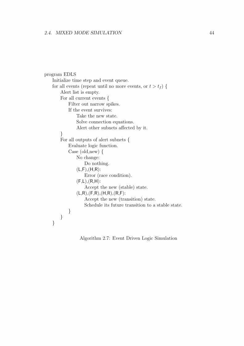
fore not necessary to process them. The EDLS (event driven logic simulation)
algorithm (2.7) touches only the subnets that are active, as indicated by events.
This method, as in all deterministic logic simulation algorithms, assumes that
the output rise and fall times are independent of the input rise and fall times,
which is not usually true. One possible remedy is to allow output transition
times to be specified as a function of input transition times, but this complicates
scheduling.
Mixed Simulation
The mixed simulation algorithm simply combines the EDCS and EDLS algorithms
with a single event queue. Logic and circuit blocks are stored separately. There
are explicit conversions between logic and circuit levels.
Logic to Circuit Conversion An equivalent circuit of a controlled voltage
source couples logic outputs to the circuit level. (Figure 2.3.) Ideally, a transition
will have a smooth transfer curve, as in figure 2.4. This conversion approximates
it to piece-wise linear, as in figure 2.5.
Note that it begins rising before the full delay time has elapsed. The signal to
be converted is taken off before the back-end delay (figure 2.6), and the delay is
2.4. MIXED MODE SIMULATION 44
program EDLSInitialize time step and event queue.for all events (repeat until no more events, or t > tf ) {
Alert list is empty.For all current events {
Filter out narrow spikes.If the event survives:
Take the new state.Solve connection equations.Alert other subnets affected by it.
}For all outputs of alert subnets {
Evaluate logic function.Case (old,new) {
No change:Do nothing.
(L,F),(H,R):Error (race condition).
(F,L),(R,H):Accept the new (stable) state.
(L,R),(F,R),(H,R),(R,F):Accept the new (transition) state.Schedule its future transition to a stable state.
}}
}
Algorithm 2.7: Event Driven Logic Simulation

2.4. MIXED MODE SIMULATION 45
Logic Subnet Circuit Subnet
yL
uC
uC = f(yL)
+
−
Figure 2.3: Logic to circuit signal conversion
φH
φH
φL φL
ti ti+1
Figure 2.4: A rising circuit switching signal (smooth)

2.4. MIXED MODE SIMULATION 46
φH
φH
φL φL
ti ti+1
Figure 2.5: A piece-wise linear rising waveform
LogicFunction
BackEndDelay
LogictoCircuitConverter
Logicout
Circuitout
Logicin
Figure 2.6: Simplified model of a logic subnet

2.4. MIXED MODE SIMULATION 47
built into the conversion. Since the rise times are known, the only time needed
from the logic simulation is the time at which it enters the transition region.
Figure 2.7: Temporally overlapping transitions
Figure 2.8: Multiple overlapping transitions
For overlapping transitions, the conversion is handled as in figures 2.7 and 2.8.
Figure 2.7 represents a pair of transitions, that result in a spike. Figure 2.8 is

2.4. MIXED MODE SIMULATION 48
three transitions, which have the effect of spending more time in the transition
region. This approach is an approximation that is not necessarily accurate in
all cases, but represents a more accurate approach than previous attempts[3][33].
Further research, including the possibility of spline interpolation, is suggested[41,
p. 113]. The URECA approach uses this ambiguity as one indicator that analog
simulation is more appropriate for this part of the circuit.
r(t) f(t)
enters R enters H enters F enters L
Figure 2.9: Thresholding
Circuit to Logic Conversion Voltage signals are transformed to logic signals
by thresholding. The voltage, relative to thresholds for high and low, is trans-
formed to the appropriate logic level (figure 2.9).
For improper signals, this simple conversion can lead to illegal logic signal
transitions (figure 2.10). The proper response would be as shown in figure 2.11.
To generate the additional transition, the converter must extrapolate backwards to

2.4. MIXED MODE SIMULATION 49
Enters R Enters L
Figure 2.10: Improper logic signal produced by thresholding
Enters R Enters LEnters F
Figure 2.11: Correct response to improper logic signal

2.4. MIXED MODE SIMULATION 50
determine the time at which the downward transition process began. This involves
descheduling, because the t2 cannot be determined until the signal crosses the low
threshold at t4. Further research is suggested[41, p. 119] with the direction of
a composite front end - back end delay model. SAMSON uses a simpler, less
accurate, approach of generating a transition to the F state when the slope of the
signal changes sign (at tx). This introduces timing errors of (tx − t2), which are
assumed to be much less than the propagation delays of the logic level subnets
driven by this signal.
Summary
SAMSON is probably the most significant prior work. Unlike other mixed-mode
simulators, it is fundamentally analog, with logic mode considered to be an accel-
eration method.
Much of the complexity and incomplete solutions are in the conversions be-
tween circuit and logic levels. The ambiguous conversions are not a problem in
URECA. Instead, they are used to indicate when the other solution method should
be used, assisting in the automatic decision making process.

Chapter 3
Implicit Mixed Mode Simulation
3.1 LU decomposition
The most common method of solving the system of equations in analog circuit
analysis is LU decomposition with forward and back substitution. This system of
equations needs to be solved on every time step and every iteration. Often only a
few values have changed between iterations, and those that have changed, changed
only by a small amount. In mixed mode simulation, some parts of the circuit do
not naturally fit this model. Some of the variables needed for this method may not
exist, or may exist only in a different form. To address this issue, we will review
the commonly used Crout method, and then extend it to fit the cases where only
parts of the matrix change and only parts of the matrix exist. It will be used as
a framework for the other methods, which will adapt dynamically.
51
3.1. LU DECOMPOSITION 52
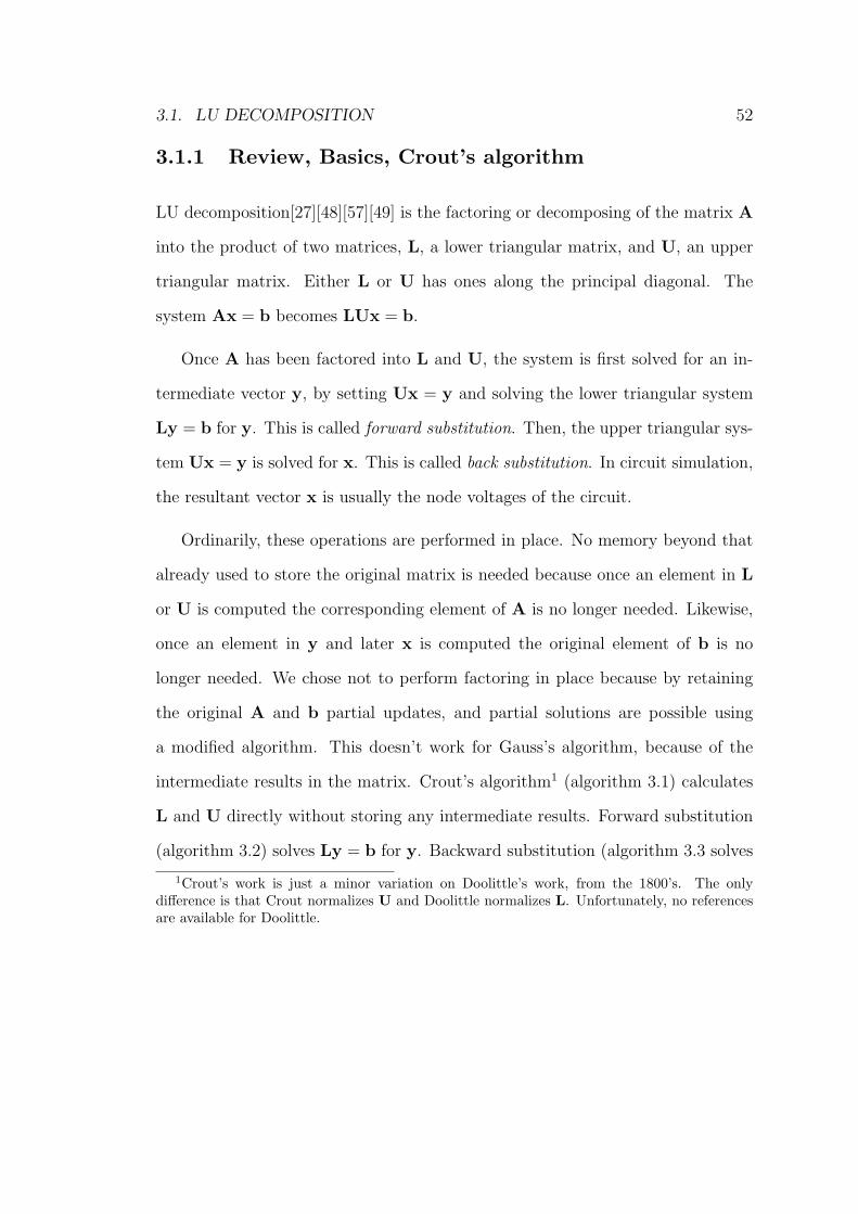
3.1.1 Review, Basics, Crout’s algorithm
LU decomposition[27][48][57][49] is the factoring or decomposing of the matrix A
into the product of two matrices, L, a lower triangular matrix, and U, an upper
triangular matrix. Either L or U has ones along the principal diagonal. The
system Ax = b becomes LUx = b.
Once A has been factored into L and U, the system is first solved for an in-
termediate vector y, by setting Ux = y and solving the lower triangular system
Ly = b for y. This is called forward substitution. Then, the upper triangular sys-
tem Ux = y is solved for x. This is called back substitution. In circuit simulation,
the resultant vector x is usually the node voltages of the circuit.
Ordinarily, these operations are performed in place. No memory beyond that
already used to store the original matrix is needed because once an element in L
or U is computed the corresponding element of A is no longer needed. Likewise,
once an element in y and later x is computed the original element of b is no
longer needed. We chose not to perform factoring in place because by retaining
the original A and b partial updates, and partial solutions are possible using
a modified algorithm. This doesn’t work for Gauss’s algorithm, because of the
intermediate results in the matrix. Crout’s algorithm1 (algorithm 3.1) calculates
L and U directly without storing any intermediate results. Forward substitution
(algorithm 3.2) solves Ly = b for y. Backward substitution (algorithm 3.3 solves
1Crout’s work is just a minor variation on Doolittle’s work, from the 1800’s. The onlydifference is that Crout normalizes U and Doolittle normalizes L. Unfortunately, no referencesare available for Doolittle.

3.1. LU DECOMPOSITION 53
Ux = y for x.
for (k = 1, . . . , n) {for (i = k, . . . , n)
lik = aik −k−1∑
p=1
lipupk
if (k ≡ n) stopfor (j = k + 1, . . . , n)
ukj =akj −∑k−1
p=1 lkpupj
lkk}
Algorithm 3.1: Crout’s algorithm
for (k = 1, . . . , n)
yk =bk −∑k−1
p=1 lkpyp
lkk
Algorithm 3.2: Forward Substitution
for (k = n, n− 1, . . . , 1)xk = yk −∑n
p=k+1 ukpxp
Algorithm 3.3: Backward Substitution
The Crout algorithm does not operate on any element in the matrix unless it
is in the row or column being eliminated. It only accesses elements of U in the
same column, above the element being eliminated, and elements of L in the same
row to the left of the element being eliminated. It eliminates elements scanning

3.1. LU DECOMPOSITION 54
ComputedNo longeraccessed
Computedandaccessed
Not yetaccessed
Beingeliminated
Figure 3.1: Crout’s algorithm

3.1. LU DECOMPOSITION 55
across rows above the diagonal and down columns below the diagonal. The status
of the elements during the process is illustrated in figure 3.1.
ComputedNo longeraccessed
Computedandaccessed
Not yetaccessed
Beingeliminated
Figure 3.2: Crout’s algorithm on a banded with spikes sparse matrix
Figure 3.2 shows the same algorithm (or essentially the same algorithm, modi-
fied to test for zero, and to skip unnecessary operations) applied to a sparse matrix
of the type resulting from a typical nodal analysis without subcircuits or any form
of partitioning. The matrix is roughly banded with varying bandwidth. A few
rows and columns have “spikes” representing many circuit or element connections
to a few nodes. To accommodate the spikes, it is necessary to test every element
for zero as the row or column is processed, even though it may not require any op-
erations. A table could be set up to minimize the testing, allowing the algorithm

3.1. LU DECOMPOSITION 56
to skip groups of elements at a time. This is often done in linked list based sparse
matrix algorithms. Nevertheless, the testing is non-trivial. The test is a simple
“if” statement, usually to see if storage is allocated, but even this can dominate
if the matrix is sparse enough, which is likely in a matrix produced by a large
circuit. Most likely, it results in a solution time for a large matrix of O(n2). The
modified algorithm presented in the next section is an improvement for this type
of matrix.
ComputedNo longeraccessed
Computedandaccessed
Not yetaccessed
Beingeliminated
Figure 3.3: Crout’s algorithm on a BBD matrix
Figure 3.3 shows the algorithm applied to a bordered block diagonal matrix of

3.1. LU DECOMPOSITION 57
the form likely to result from subcircuit expansion or explicit partitioning. The
blocks along the diagonal represent subcircuits. The border represents connections
between them. Scanning across a row (or column) operates on elements within
the block being worked on, and in the border. No access is needed to blocks
belonging to other subcircuits. If subcircuit expansion is applied recursively, the
blocks themselves could be bordered block diagonal, and the same conditions
apply.
The next section describes a modified method that is a better fit to the type
of matrix resulting from nodal analysis of circuits.
3.1.2 Sparse vector method
Storage
Traditional LU decomposition based simulators use generic sparse matrix storage,
that does not exploit the form of the matrix. The usual method is a pair of linked
lists, which is well documented elsewhere[17][57][31], and will not be repeated
here.
The approach used here is a vector scheme[9], that uses two pointer arrays and
allows access to the sparse matrix element in the same time ordinarily needed to
access an element in a dense matrix, thus eliminating the overhead of the more
complicated indexing scheme. Also, the number of tests for zero elements required
is reduced to one per column (or row). The scheme also allows blocks representing

3.1. LU DECOMPOSITION 58
subcircuits to be stored in a compact form that still appears compact as part of
the large matrix. This method was inspired by a paper by Dongarra, Gustavson
and Karp on dense matrices on a vector machine[16].
The matrix is stored by row below the diagonal, and by column above. The
part above the diagonal is stored backwards. This enables the diagonal itself to be
part of both the upper and lower parts, without duplication. Two pointer arrays
hold pointers to the apparent location of row 0 of each column, and column 0 of
each row. It doesn’t matter that row 0 and column 0 do not exist. An integer
array basenode holds the number of the lowest node connected to each node.
At this point, we digress, and discuss usual methods of storing two-dimensional
matrices in the language “C”. Like most other languages, C supports two-dimen-
sional static arrays. Indices start at 0, and they are stored by row. Another
approach is to set up an array of pointers, one pointer for each row, and n row
vectors. The pointer array and all the row vectors are dynamically allocated by a
call to the library function “calloc”. Using this method, the size of the matrix can
be adjusted to fit the problem, the space can be returned to the system when it
is no longer needed, and a new array, of a possibly different size, can be allocated
for a new problem. Machine memory limits do not influence coding at all. The
C code to access an array stored this way looks exactly the same as code for a
static two-dimensional array, except that the requirement to keep track of the
allocated size is eliminated. It is implicit in the pointers. The machine code
generated accesses an element by indirection through a pointer rather than by a

3.1. LU DECOMPOSITION 59
multiplication and an addition. The rows of the array can be of different lengths.
To start from an index other than 0 it is simply a matter of adjusting the pointer
so it points to where location 0 would be if it were there. For example, to start
at 1, decrement the row pointer before storing it. To start at 7, subtract 7 before
storing it. (In C, pointer arithmetic takes into account the size of the item being
pointed to.)
Storing the lower triangular part of the matrix is exactly the same as a stan-
dard matrix except for the pointer adjustments. The upper triangular part is
similar except that row and column are interchanged and the vector direction is
backwards. To accomplish this the pointer points to the end of the vector instead
of the beginning, to the apparent location of element 0, and the row number has
its sign changed.
When memory is allocated row n and column n are allocated as a unit, with
the diagonal element common to both. The row pointer points to one end of it,
the column pointer to the other.
Consider the matrix:
11 12 0 0 021 22 23 0 00 32 33 34 350 0 43 44 00 0 0 54 55
(3.1)
This matrix is stored in the linear array:
[11 21 22 12 32 33 23 43 44 34 0 54 55 0 35
](3.2)

3.1. LU DECOMPOSITION 60
It can be broken into 5 vectors:
[11
]
[21 22 12
]
[32 33 23
]
[43 44 34
]
[0 54 55 0 35
](3.3)
The basenode integer array contains a list of the lowest node connected to each:
[1 1 2 3 3
](3.4)
In this list, node 1 has no connections lower than 1. Node 2 connects to as
low as 1. Node 5 connects to as low as 3. Connections to higher nodes are not
considered.
The pointer arrays point to what would be row or column 0, if they existed.
The row pointer array points below the actual storage:
[−1 0 2 4 7
](3.5)
The column pointer array points above the actual storage:
[1 4 8 12 17
](3.6)

3.1. LU DECOMPOSITION 61
To access element 32 (row 3, column 2, below the diagonal) take the base of
row 3 (2), and add 2. It is stored in location 4. To access element 34 (row 3,
column 4, above the diagonal) take the base of column 4 (12), and subtract 3. It
is stored in location 9.
The added complexity in working with the matrix, as compared to the dense
case, is insignificant, consisting of checking to see whether it is above or below
the diagonal, and using the appropriate code. The difference is reversing row and
column, and possibly negating the row number. It often is known whether the
element being accessed is above, below, or on the diagonal, so the appropriate
code can be used directly. To access the diagonal element, either code can be
used, or another pointer array can point directly to the diagonal element. Most
of the added complexity is in setting up the system, which needs to be done only
once, for many solutions of systems with the same structure. Access time is often
further reduced because the elements of the vector are used in order, so finding
an element is done simply by incrementing or decrementing a pointer.
Solving
By calculating the L and U factors in a different order the algorithm becomes a
better fit to the allocation scheme. (Figure 3.4. Algorithm 3.4.)
Adding a simple test for the length of the vector eliminates the need to access
the zeros outside the band. (Algorithm 3.5.) The basenode table (the lowest node
connecting to a given node, or the the index of the lowest numbered element in a

3.1. LU DECOMPOSITION 62
Computedandaccessed
Not yetaccessed
Beingeliminated
Figure 3.4: Modified Crout’s algorithm

3.1. LU DECOMPOSITION 63
l11 = a11
for (k = 2, . . . , n){u1k =
a1k
l11
for (i = 2, . . . , k − 1){uik =
aik −∑i−1p=1 lipupk
lii}lk1 = ak1
for (j = 2, . . . , k){lkj = akj −
j−1∑
p=1
lkpupj
}}
Algorithm 3.4: Modified Crout Algorithm
given row or column. In any row or column, the elements from 1 to some k will
be zero. Elements from k + 1 up to the diagonal will be non-zero, or subject to
being filled in, so are treated as if they were non-zero. Thus, an entire column or
row can be tested for its zeros in a single test. There are now only O(n) of these
tests.
Figure 3.5 shows the algorithm applied to the same matrix as figure 3.2, at
several stages in the decomposition. Figure 3.6 shows the algorithm applied to
a BBD matrix resulting from subcircuit expansion. While working on elements
within a block there are no accesses outside the block. Because of this, it is possible
to decompose the blocks representing subcircuits separately without concern for
the remainder of the system. If two or more are linear and identical, their matrix

3.1. LU DECOMPOSITION 64
l11 = a11
for (k = 2, . . . , n){b = basenode(k)if (b < k){
s = max(basenode(i), basenode(k))
usk =ask
lssfor (i = b + 1, . . . , k − 1){
uik =aik −∑i−1
p=s lipupk
lii}s = max(basenode(k), basenode(j))lks = aks
for (j = b + 1, . . . , k){lkj = akj −
j−1∑p=s
lkpupj
}}
}
Algorithm 3.5: Modified Crout with Zero Bypass

3.1. LU DECOMPOSITION 65
ComputedNo longeraccessed
Computedandaccessed
Not yetaccessed
Beingeliminated
ComputedNo longeraccessed
Computedandaccessed
Not yetaccessed
Beingeliminated
Figure 3.5: Modified Crout’s algorithm on a banded with spikes sparse matrix

3.1. LU DECOMPOSITION 66
ComputedNo longeraccessed
Computedandaccessed
Not yetaccessed
Beingeliminated
Figure 3.6: Modified Crout’s algorithm on a BBD matrix

3.1. LU DECOMPOSITION 67
blocks will also be identical, before and after decomposition. They can thus share
storage, and be decomposed only once.
3.1.3 Solving only part of the matrix
Circuit simulation requires repeated solutions of matrices that are almost the
same. After the first solution the matrix is changed in only some of its locations.
It is desirable to solve again without repeating all the work.
There are several methods published for recomputing the inverse or LU factors
of matrices with low-rank modifications.[22][37]. The method used here requires
storage of both the original matrix A and the decomposed matrices LU. Since the
original matrix is maintained, only those elements that change need to be rebuilt.
The change process is to add the difference between the old and new values, and
flag those elements as changed. After the changes are made to A, the flags tell
which parts of LU need to be recomputed.
From the algorithm and definition of LU decomposition, an element lij is
calculated by:
lij = aij −j−1∑
p=1
lipupj. (3.7)
From this, the value lij depends only on elements of L and U for nodes m < j.
For a bordered band matrix, lip ≡ 0 for p < basenode(i) and upj ≡ 0 for
p < basenode(j), so lij depends only on nodes m such that maxbasenode(i, j) ≤m < j. For a BBD matrix, basenode(i or j) is always in the same block, or
maxbasenode(i, j) ≥ q, where q is the lowest node in the block. So, lij depends

3.1. LU DECOMPOSITION 68
only on elements of LU within the same block. For elements in the border, upj ≡ 0
for p < basenode(j), so it, too, depends only on elements within the corresponding
block, and that segment of its own row.
Elements above the diagonal are handled similarly, based on
uij =aij −∑i−1
p=1 lipupj
lii(3.8)
To find which elements are affected by changes to a particular element aij (the
converse of the above), it is only necessary to look at the formulae for lpq and
upq to see which contain the corresponding lij or uij, then apply this criterion
recursively.
For a sample element aij above the diagonal, the elements {ukj|i ≤ k < j}are affected, and need to be recalculated. The change also affects {lkj|j ≤ k ≤n}, directly. The row {ujp|j < p ≤ n} needs to be renormalized as a result of
the change to ljj. The elements ukp and lkp, where j ≤ k, p ≤ n, needs to be
recalculated as a result of the other changed to L and U. A similar analysis could
be applied to changes below the diagonal.
For a BBD matrix the direct changes do not affect the zeros outside the block
being changed and the border. Since other changes are the result of propagation
of changes to the column of the initial change, they do not propagate outside the
block containing the initial change, except to the border.
To keep track of what has changed, it is known that changes are confined to
the same block, and to the border. Changes propagate only to higher numbered

3.2. ITERATIVE METHODS 69
nodes. After any set of modifications, the new decomposition starts at the lowest
numbered node in a block that changed, and continues to the end of that block.
This simplistic approach could waste some time because only the column directly
below an element in U, or row directly to the right of an element in L actually
needs to be redone. Most changes, other than those on the diagonal, are in groups
of four, so a change to aij usually is accompanied by changes to aji, aii, ajj. In this
case, there are no wasted operations. In the case where the update is asymmetric
about the diagonal, the only problem with this approach is a few extra operations.
After decomposing A into LU, the system Ly = b must be solved for y
(forward substitution). A particular element yk is calculated by
yk =bk −∑k−1
p=1 lkpyp
lkk
(3.9)
This is similar to the formula for u, so the same arguments on change propagation
apply. The change only affects the corresponding block.
Back substitution solves for the node voltages. It will be shown later that
the propagation of changes is predicted by the fanout list, and its values are not
necessarily calculated from this matrix, so it can be managed by the selective
trace algorithm.
3.2 Iterative methods
Nonlinear equations are almost always solved by iterative methods. Most circuit
simulators use either Newton’s method or a relaxation method. Depending on the

3.2. ITERATIVE METHODS 70
equations being solved, either may work better. One or both may not work at all.
We now review the methods used, and how they fit in a unified data structure to
allow the free choice at run time. We also cast logic simulation as an abstraction
of iterative methods. For formal analysis of these methods, the reader is referred
to several texts on iterative solutions of equations[36][56][52].
3.2.1 Fixed Point Iteration
Solving nonlinear equations is generally done by some form of fixed point iteration.
Given a function f(x), it is desired to find a root x(∗) of that function2. In any
fixed point method, an iteration function g(x) is defined such that x = g(x).
Given a starting point x(0), applying the iteration x(k) = g(x(k−1)) generates a
sequence {x(k)}∞k=0. Hopefully, x(k) → x(∗) as k →∞.
The generic fixed point method uses an iteration function of the form of:
g(x) = x− α−1f(x) (3.10)
The iteration is then:
x(k) = x(k−1) − α−1f(x(k−1)) k = 1, 2, . . . (3.11)
A suitable value for α, and a suitable starting point, x(0), will result in con-
vergence to the root. An unsuitable value for α or starting point will result in
non-convergence or slow convergence.
2In this section, the notation x(k) refers to the kth iteration of x.

3.2. ITERATIVE METHODS 71
This can be extended to an n dimensional function F by replacing α with a
nonsingular matrix A. The n dimensional method is
x(k) = x(k−1) −A−1f(x(k−1)) k = 0, 1, . . . (3.12)
The resulting system of linear equations is solved either by LU decomposition,
or by relaxation. Both methods are commonly used in circuit simulators. Relax-
ation methods iterate directly. LU decomposition based methods reformulate the
equation to either
Ax(k) = Ax(k−1) − f(x(k−1)) k = 1, 2, . . . (3.13)
or
A(x(k) − x(k−1)) = −f(x(k−1)) k = 1, 2, . . . (3.14)
The most commonly used form of the fixed point iteration is Newton’s method,
where α = f ′(x), and is reevaluated every iteration. In the n dimensional case,
the matrix A is the Jacobian, a matrix of partial derivatives, aij = ∂fi(x)/∂xj for
i, j = 1, . . . , n. In SPICE and most classic circuit simulators, the form 3.13 is used.
In the linear case it maps to directly to Yv = i, where Y is the admittance matrix,
v is the vector of unknown node voltages, and i is the vector of fixed currents.
When the initial guess is close enough, the method has quadratic convergence. It
may converge linearly or not at all with a poor initial guess.
A variation on Newton’s method differs only in that it does not recalculate the
derivatives every iteration[2]. This method, strictly, has only linear convergence,
but if the derivative only changes by a small amount, performance can be almost

3.2. ITERATIVE METHODS 72
as good as Newton’s method. The advantage is that time can be saved by not
calculating all the derivatives and the LU decomposition every time. Solving the
system of equations is only forward and back substitution, for that block of the
matrix.
Alternatively, calculation of the derivative may be avoided by using a difference
approximation:
f ′(x(k)) ≈ f(x(k) + h(k))− f(x(k))
h(k)(3.15)
The secant method uses h(k) = x(k−1) − x(k) and approximates the derivative by:
f ′(x(k)) ≈ f(x(k−1))− f(x(k))
x(k−1) − x(k)(3.16)
The regula falsi method uses h(k) = x−x(k) where x is usually an old value of x(k)
chosen so that x and x(k) bracket the root. It approximates the derivative as:
f ′(x(k)) ≈ f(x)− f(x(k))
x− x(k)(3.17)
These discrete methods have slower convergence than Newton’s method, but
may converge when Newton’s method does not and avoid computing the deriva-
tive. The secant method has order 1.6. The regula falsi method is linear. Using
an old approximation of the derivative is usually linear. The regula falsi method
is often used when Newton’s method fails, because it brackets the root.
In circuit simulation, the matrices used in 3.13 are built by summing of the
individual circuit elements, as described in section 2.2.1. Keeping the old deriva-
tive avoids updating the matrix, which makes it possible to avoid calculating

3.2. ITERATIVE METHODS 73
its decomposition. (See 3.1.3.) The secant method uses a prior value to avoid
computing the derivative, with some sacrifice in convergence order. It is used
for secondary effects in device models, where there is little change per iteration,
but would involve a considerable cost to compute the derivative correctly. The
regula falsi method can be used as a backup, when Newton’s method is failing
to converge. All these variations fit the model of 3.13, and a new choice can be
made for any element at any time. If an entire subcircuit can use old derivative
values, that block of the matrix A is unchanged, saving the time needed for the
LU decomposition for that block.
3.2.2 Relaxation methods
A basic principle for generating iterative methods is splitting [36, p. 217]. Given
a linear system Ax = b, A can be decomposed into the sum of two matrices
A = B−C, where B is nonsingular and the system Bx = d is easy to solve. The
iterative method can be defined by:
Bx(k) = Cx(k−1) + b k = 1, 2, . . . (3.18)
By rearranging terms:
x(k) = B−1(Cx(k−1) + b) k = 1, 2, . . . (3.19)
or
x(k) = x(k−1) −B−1(Ax(k−1) − b) k = 1, 2, . . . (3.20)
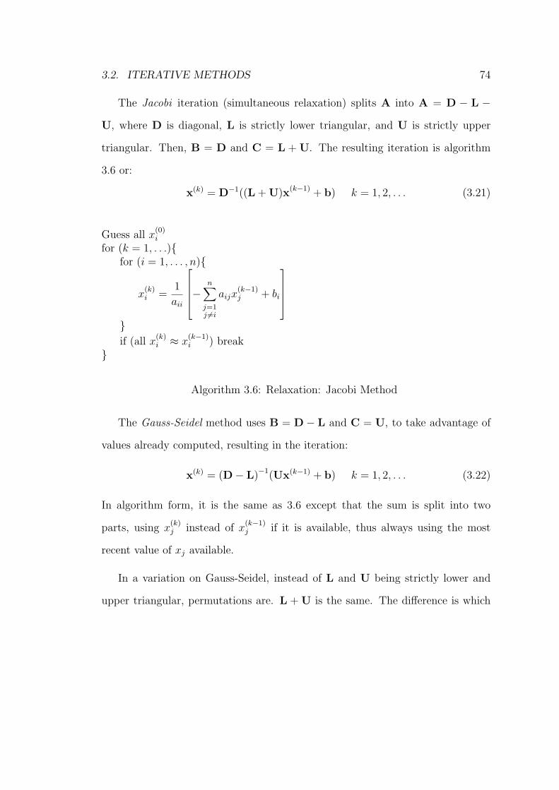
3.2. ITERATIVE METHODS 74
The Jacobi iteration (simultaneous relaxation) splits A into A = D − L −U, where D is diagonal, L is strictly lower triangular, and U is strictly upper
triangular. Then, B = D and C = L + U. The resulting iteration is algorithm
3.6 or:
x(k) = D−1((L + U)x(k−1) + b) k = 1, 2, . . . (3.21)
Guess all x(0)i
for (k = 1, . . .){for (i = 1, . . . , n){
x(k)i =
1
aii
−
n∑
j=1j 6=i
aijx(k−1)j + bi
}if (all x
(k)i ≈ x
(k−1)i ) break
}
Algorithm 3.6: Relaxation: Jacobi Method
The Gauss-Seidel method uses B = D − L and C = U, to take advantage of
values already computed, resulting in the iteration:
x(k) = (D− L)−1(Ux(k−1) + b) k = 1, 2, . . . (3.22)
In algorithm form, it is the same as 3.6 except that the sum is split into two
parts, using x(k)j instead of x
(k−1)j if it is available, thus always using the most
recent value of xj available.
In a variation on Gauss-Seidel, instead of L and U being strictly lower and
upper triangular, permutations are. L + U is the same. The difference is which

3.3. LOCAL STEP CONTROL 75
elements are part of L and which part of U. Mathematically, the iteration func-
tion is the same, but elements of x are solved in a different order, equivalent to
solving a permutation of A and b. The order is appropriate for the permuta-
tions used, which changes dynamically on each iteration. The algorithm changes
only in that the i loop is not done in order, and that all xj are not computed
every time. This (actually SOR) is the selective trace driven algorithm used in
SPLICE2[32][44][25].
For nonlinear circuits, A is the matrix of partial derivatives (the Jacobian ma-
trix), resulting in a combined relaxation-Newton method. In practice, the matrix
A is not formed explicitly. The partial derivatives are not actually calculated.
Logic simulation is simply an abstraction of circuit simulation, by a relaxation
method. The only difference is that the values are discrete logic states, instead of
continuous values.
3.3 Local step control
3.3.1 Solving part of the circuit
LU decomposition on part of a matrix was discussed in 3.1.3. Since the original
matrix A is kept, and not over-written by LU, it is possible to change it when
necessary. Alternatively, the change in the derivative may be small enough that
a partial model evaluation can be done, which will update only the right side of
the system of equations.

3.3. LOCAL STEP CONTROL 76
The matrix was built by summing the Norton equivalent of all circuit branches.
To update the existing matrix, conceptually the method is to subtract the old
value, and add the new value. To have the same effect, the actual code adds the
difference between the old and new values. If too much accumulated round-off
error is suspected, the matrix element can be rebuilt according to 3.7 or 3.8. As a
test to see if the effect propagates to the rest of the matrix, the difference added
can be compared to a tolerance. If the change exceeds a tolerance, that node is
marked as changed. Changes to the right side vector are handled similarly, and
separately. In general, many changes will be made to the right side, but many
fewer to the matrix.
As the changes are made, the nodes being changed are tagged, so that the
LU decomposition can start there, bypassing parts that did not change. Decom-
position stops at the end of a block. An array of flags indicates which nodes
changed.
The simulation is event driven, using selective trace to control which elements
are evaluated, and using a bypass to skip parts of the decomposition of the Jaco-
bian. (Algorithm 3.7)
In comparison, SPICE will bypass model evaluation when the voltages at the
terminals of a device are close enough (v(k)− v(k−1) < VNTOL), but will not bypass
the decomposition phase. The matrix is built as usual, using old values if the
model evaluation is being bypassed. SAMSON also uses bypass, not selective
trace, to skip model evaluation in the same way, with a “dormancy check” to see
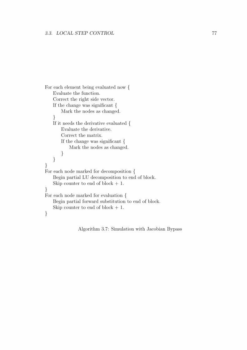
3.3. LOCAL STEP CONTROL 77
For each element being evaluated now {Evaluate the function.Correct the right side vector.If the change was significant {
Mark the nodes as changed.}If it needs the derivative evaluated {
Evaluate the derivative.Correct the matrix.If the change was significant {
Mark the nodes as changed.}
}}For each node marked for decomposition {
Begin partial LU decomposition to end of block.Skip counter to end of block + 1.
}For each node marked for evaluation {
Begin partial forward substitution to end of block.Skip counter to end of block + 1.
}
Algorithm 3.7: Simulation with Jacobian Bypass
3.3. LOCAL STEP CONTROL 78
if the bypass is valid. SAMSON will bypass the decomposition of the Jacobian
for whole subcircuit blocks, based on user partitioning.
3.3.2 The event queue
An event is something happening that has some effect on the circuit. In logic
circuits, the concept of an event is clear, because either something is happening,
or nothing is happening. There are no questionable areas. In analog circuits, the
decision is more subtle.
In logic circuits, an event is any signal changing. Initially, events occur when
an external signal changes. These are the easiest to detect, because they are listed
in the circuit description. When a signal propagates, it generates more events.
In analog circuits, a threshold determines when a signal is considered to have a
significant change.
These are some conditions that are considered to be “events”:
1. Abrupt change of an input.
2. Significant change of an input.
3. An internal voltage or current abruptly changes.
4. An internal voltage or current changes significantly.
5. A device crosses a region boundary.
6. It is time for another step, as in integrating a capacitor.

3.3. LOCAL STEP CONTROL 79
7. Integration truncation error is out of bounds.
8. Another iteration is needed.
An event queue stores the list of pending events, sorted by increasing time.
An event has two components: time and description. The description is a list of
things to do. Here, it is a list of branches to process.
Unlike digital simulation, in analog simulation many events can occur at an
approximate time. Since many events are generated by an error or signal change
exceeding a tolerance, it is often permissible to change the time at which an event
is considered to occur so that many events can be considered to occur at the
same time. An example of this is the integration time steps for a capacitor. If
integration time steps are smaller than they need to be, the solution accuracy will
be increased. The extra processing time of more steps may be offset by having
them synchronized.
SPLICE and SAMSON both will back up time if truncation error is too high.
URECA will not back up time, but will instead accept occasional steps that are
out of tolerance.
3.3.3 Selective trace applied to LU decomposition
Selective trace, as implemented in logic simulators, uses a fan-out list to deter-
mine how changes to the system propagate. The event queue contains a list of
elements to process, sorted by the time at which to process them. In trace driven
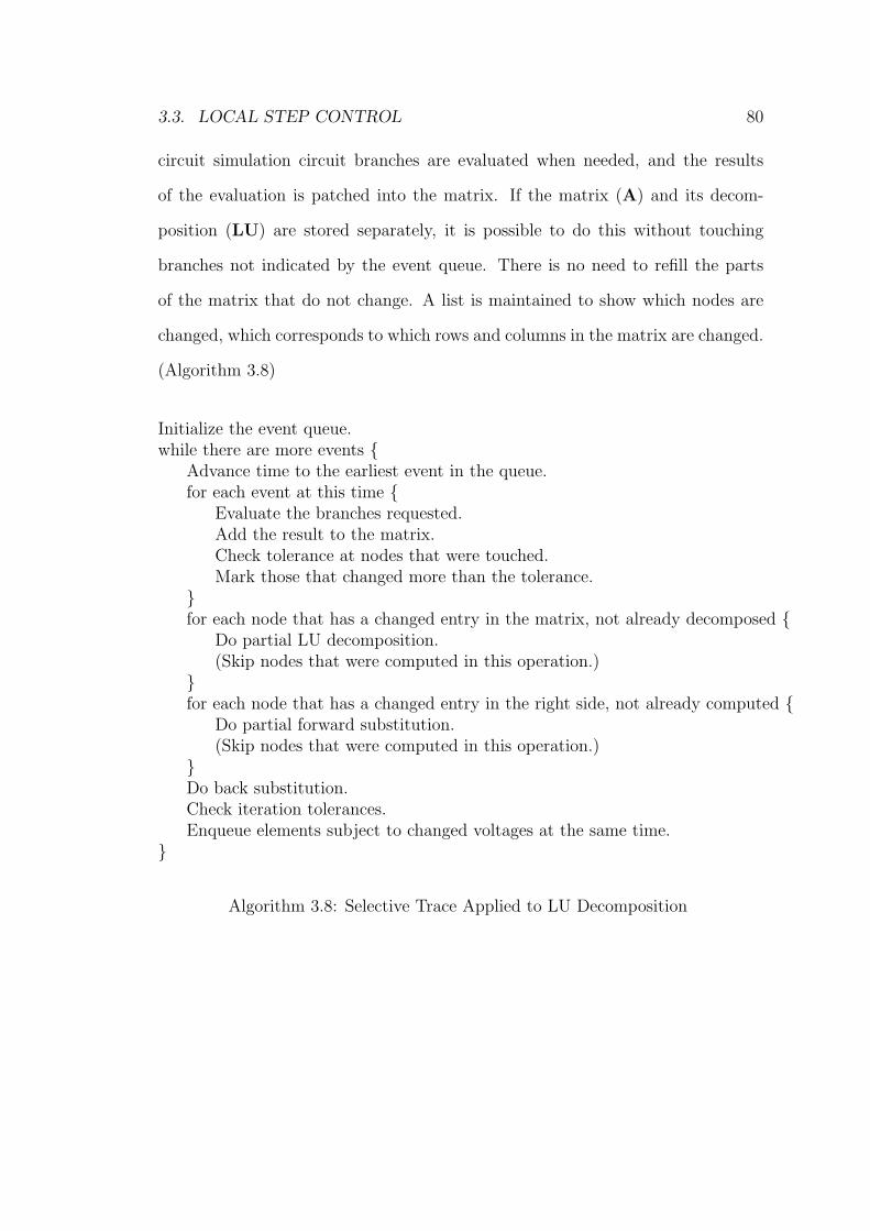
3.3. LOCAL STEP CONTROL 80
circuit simulation circuit branches are evaluated when needed, and the results
of the evaluation is patched into the matrix. If the matrix (A) and its decom-
position (LU) are stored separately, it is possible to do this without touching
branches not indicated by the event queue. There is no need to refill the parts
of the matrix that do not change. A list is maintained to show which nodes are
changed, which corresponds to which rows and columns in the matrix are changed.
(Algorithm 3.8)
Initialize the event queue.while there are more events {
Advance time to the earliest event in the queue.for each event at this time {
Evaluate the branches requested.Add the result to the matrix.Check tolerance at nodes that were touched.Mark those that changed more than the tolerance.
}for each node that has a changed entry in the matrix, not already decomposed {
Do partial LU decomposition.(Skip nodes that were computed in this operation.)
}for each node that has a changed entry in the right side, not already computed {
Do partial forward substitution.(Skip nodes that were computed in this operation.)
}Do back substitution.Check iteration tolerances.Enqueue elements subject to changed voltages at the same time.
}
Algorithm 3.8: Selective Trace Applied to LU Decomposition

3.4. LOGIC SIMULATION 81
3.4 Logic simulation
In developing the logic simulation algorithms for implicit mixed-mode simulation,
there are several goals to be considered.
1. Logic is considered to be an abstraction of a subset of the analog domain.
A logic block, like an analog functional block, takes the inputs, applies
some transfer function, and produces the outputs. The digital signals are
abstractions of the analog signals: voltage and resistance. With this in
mind, there is no unknown state, since it cannot be represented in the analog
domain.
2. The form chosen, both the internal data structures and the netlist descrip-
tion, must fit in a primarily analog simulator. A logic element is considered
to be similar to a circuit element, device, or subcircuit. A logic technology
description is considered to be similar to a transistor or mosfet technology
description for example, a “.model card” in SPICE. Logic values at nodes
are stored in an array that parallels the voltage array.
3. The logic algorithms employed use the same techniques as traditional logic
simulators, in hopes that for purely logic circuits, the “mixed” simulation
(which is not really mixed) will not result in a significant penalty in time
or space. Since the analog model also exists, there is a significant cost in
space, slightly worse than a fully analog simulator.

3.4. LOGIC SIMULATION 82
3.4.1 Logic States
It is necessary to abstract the voltage and resistance into discrete states for logic
simulation. The states are based on a correspondence to technology dependent
tables. URECA supports only one technology (CMOS), but to be useful to a
practicing engineer, different technologies must be supported. Some significant
other technologies include NMOS, TTL, ECL, and diode logic. All of these have
binary states (true and false) when operating correctly. Other states, including
in-transition and unknown, are variations on the binary states that show history.
The “hi-z” state, which is used extensively in some logic families, is part of an
abstraction of the resistance. The resistance, when operating correctly, is normally
some low value or some high value. It is usually either constant, changes in
synchronization with the voltage, or is controlled by some input. The choice of
values is again technology dependent.
In a typical gate, the output transition follows some finite time after the input
transition. This is indicated by an in transition state, either rising or falling. The
internal representation of the transition states is to store both the new and old
values. As an approximation, the transition state can show either that the signal
is in the transition region, or it is waiting. The transition state is not propagated.
It is only used internally to the logic model to show that the output will change
soon. Thus, any transition has a new and old value. The signal that propagates
is the old value. After a specified delay the new value propagates to the old value.
The simple algorithm for evaluating a gate is shown in algorithm 3.9.

3.4. LOGIC SIMULATION 83
On an input (old) transition {Evaluate the logic function based on old inputs.If there is a state change {
Place the result in new (indicating a transition state).Enqueue the change to the final state.
}}When the time for the final change arrives {
Copy new to old. (Propagate the change.)Evaluate fanout elements.
}
Algorithm 3.9: Gate Evaluation
The strength or resistance state (strong vs. weak) either tracks the voltage
state, is constant, or is driven by another input. The exact behavior depends on
the logic family. In an open collector transistor logic family all lows will be strong,
and all highs will be weak. In CMOS both states will be strong, but a transmission
gate will propagate its input voltage, with the control terminal deciding whether
it is strong or weak. When only one element drives a node, the strength makes
no difference. When two or more elements drive a node, any conflict is a fault
that will cause a switch to analog simulation. If exactly one is strong, all the weak
signals are ignored. If more than one is strong and they have the same state, that
is the state that is propagated. If they have different states, an error exists, which
also switches to analog simulation. If all are weak, and the states disagree, analog
simulation is used. A passive pull-up is a special element that is ordinarily weak
but becomes strong if everything else connecting to that node is weak.

3.4. LOGIC SIMULATION 84
3.4.2 Inconsistencies
in1
in2
out(internal)
out(propagated)
delay delay
Figure 3.7: Distinct transitions
The above abstractions work when all signals are proper, that is when there are
no race or spike conditions. In race conditions signals arrive at a gate at different
times that are not sufficiently different to be considered independently. The second
transition may arrive after the first by a time that is less than the propagation
delay of the gate.
In the figures 3.7, 3.8, and 3.9 two inputs are applied to an and gate.
In figure 3.7 in2 follows in1, with enough time to allow the first to propagate
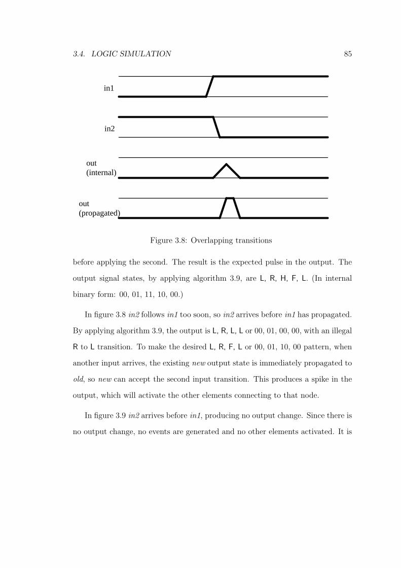
3.4. LOGIC SIMULATION 85
in1
in2
out(internal)
out(propagated)
Figure 3.8: Overlapping transitions
before applying the second. The result is the expected pulse in the output. The
output signal states, by applying algorithm 3.9, are L, R, H, F, L. (In internal
binary form: 00, 01, 11, 10, 00.)
In figure 3.8 in2 follows in1 too soon, so in2 arrives before in1 has propagated.
By applying algorithm 3.9, the output is L, R, L, L or 00, 01, 00, 00, with an illegal
R to L transition. To make the desired L, R, F, L or 00, 01, 10, 00 pattern, when
another input arrives, the existing new output state is immediately propagated to
old, so new can accept the second input transition. This produces a spike in the
output, which will activate the other elements connecting to that node.
In figure 3.9 in2 arrives before in1, producing no output change. Since there is
no output change, no events are generated and no other elements activated. It is
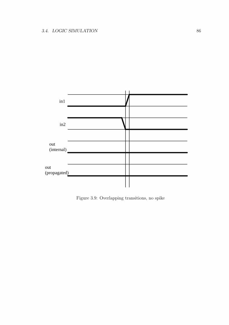
3.4. LOGIC SIMULATION 86
in1
in2
out(internal)
out(propagated)
Figure 3.9: Overlapping transitions, no spike
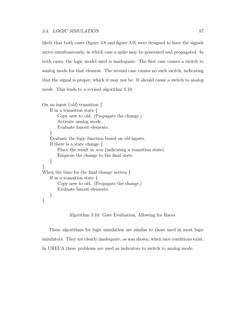
3.4. LOGIC SIMULATION 87
likely that both cases (figure 3.8 and figure 3.9) were designed to have the signals
arrive simultaneously, in which case a spike may be generated and propagated. In
both cases, the logic model used is inadequate. The first case causes a switch to
analog mode for that element. The second case causes no such switch, indicating
that the signal is proper, which it may not be. It should cause a switch to analog
mode. This leads to a revised algorithm 3.10.
On an input (old) transition {If in a transition state {
Copy new to old. (Propagate the change.)Activate analog mode.Evaluate fanout elements.
}Evaluate the logic function based on old inputs.If there is a state change {
Place the result in new (indicating a transition state).Enqueue the change to the final state.
}}When the time for the final change arrives {
If in a transition state {Copy new to old. (Propagate the change.)Evaluate fanout elements.
}}
Algorithm 3.10: Gate Evaluation, Allowing for Races
These algorithms for logic simulation are similar to those used in most logic
simulators. They are clearly inadequate, as was shown, when race conditions exist.
In URECA these problems are used as indicators to switch to analog mode.

3.5. MIXED SIMULATION 88
3.5 Mixed simulation
The essence of mixed-mode simulation is that two or different types of simulation
can be applied in the same circuit. This section discusses the data structures and
decision algorithms to combine logic and circuit simulation.
3.5.1 Data Structures
The value at any node can be either continuous (voltage) or discrete (logic state).
In addition, other information could also be useful at each node. A node value
array holds the additional information:
Logic value. Two bits, new and old, represent the logic state as true or false. In
stable states both the new and old values are the same. If they are different,
the state is in transition. This translates to voltage in analog simulation.
The definitions of true and false, from the analog viewpoint, are determined
by user specified process dependent parameters.
Safe logic value. It is probable that some states will be calculated incorrectly
because of iteration. The values at the start of iteration are stored here, to
keep the history, not contaminated by false iteration values.
Logic strength. Two bits, new and old, represent the strength as either strong
or weak. The state definitions here are also dependent on user specified pa-
rameters. It translates to resistance in the analog domain. Usually, strong
3.5. MIXED SIMULATION 89
corresponds to a low resistance and weak to a high resistance, possibly infi-
nite.
Mode. The mode can be either analog or digital depending on how the value at
the node was calculated. It is set when the value (voltage or logic state)
is calculated, and is used in mode conversion. If the mode is digital, the
logic value was calculated directly by a logic gate, the analog voltage is
estimated, if needed, from the logic state. If the mode is analog, the voltage
is calculated by solving the network equations. The logic state is calculated
from the analog voltage by thresholding.
Quality. There is an indication of the “quality” of a supposedly digital signal.
The number is an integer. A value of zero means it is good enough to be
simulated as digital. If a signal is found to be defective in some way (too slow
or out of range) quality is set to the value of transits, usually 2, and analog
mode is selected. When a clean transition occurs, quality is decremented.
When it becomes zero, it is considered clean enough for digital simulation.
Old quality. Another copy of quality for iteration.
Logic family. The conversion between digital and analog information differs be-
tween logic families. If devices in different families connect to the same
node, the interfacing must be analog. The logic family value is a pointer
representing the model card of the family that generated the digital infor-
mation.

3.5. MIXED SIMULATION 90
Iteration number tags. Two integers, one for digital, one for analog, keep track
of when the node was last updated. If the digital information is more recent
than the analog information and analog information is needed, a conversion
function can be called to generate up-to-date analog information. A similar
conversion converts analog to digital, if the analog information is newer.
Last change time. The time at which this node was last updated. This time is
either the present time, or in the past.
Time difference. The difference between the last update and the one before
that. It is used in integration and slope checking for analog to logic conver-
sion.
Next event time. If an event is scheduled at this node, its time is stored here.
This time is usually in the future. A zero means there are no events scheduled
at this node.
Voltage. This is the most recent voltage at this node, usually calculated either by
the standard analog simulation method, or by a conversion from the digital
value. It is valid at the last change time.
Old voltage. The voltage one time step ago is used in integration, and to de-
termine slope for analog to logic conversion. This voltage was valid time
difference before the most recent voltage.
Both analog and digital values can exist at any node. The mode shows whether
the node is analog, with digital derived from it, or digital, with an analog approx-

3.5. MIXED SIMULATION 91
imation derived from the digital. The iteration tags indicate which are valid. If
one is older than the other, the older one is not valid and must be regenerated.
The admittance (Jacobian) matrix is allocated for all parts of the circuit,
assuming that it may be all analog. For parts of the circuit that are simulated as
digital, the corresponding parts of the matrix are not filled or used. In a program
intended for commercial use, the matrix would be allocated by subcircuit blocks,
with the allocation for the hopefully digital blocks deferred until they are needed.
This change would result in a considerable reduction of memory requirements for
large circuits that are primarily digital.
3.5.2 Choice of methods, how?
Given that both analog and digital modes exist it is obviously necessary to choose
which mode to apply where. Sometimes it seems obvious. Only one model for
an element exists. Usually the user does specify, but is often wrong. Analog
elements will necessarily need analog simulation. Logic elements apparently need
logic simulation, but this is not always true. Race conditions and poorly shaped
signals can make logic simulation misleading. It is possible that a logic device was
misused deliberately by the user. Two examples of this are making an oscillator
out of two gates, and using a gate as an amplifier. The decision of which mode to
use is made for each logic element, at run time, based on a set of rules.
The rules for deciding which mode to use are based on some assumptions:
1. Both analog and digital information are available at any node, at the request

3.5. MIXED SIMULATION 92
of any element attached to that node.
2. The conversion will be made on request. If the result is suspect, it will be
tagged for analog simulation.
3. A logic block with digital inputs will be simulated as analog, resulting in
analog outputs, if any input or combination has a questionable state. This
will force the logic block driving it to generate analog outputs, even if it is
simulated as digital.
4. A logic block with analog inputs will be simulated as digital only if the input
logic states can easily be determined from the voltages.
5. A logic block with digital inputs from a different logic family will be simu-
lated as if its inputs were analog. This means that it may be simulated as
digital, but the conversions take place.
The application of these rules will become apparent in the next section: circuit
to logic conversion. One important basis for the mode decision is the difficulty of
making the conversions between analog and digital type signals.
3.5.3 Circuit to Logic Conversion
Voltage signals are transformed to logic signals by thresholding (figure 3.10),
roughly as in SAMSON. (See section 2.4.1.) For improper signals this simple
conversion leads to illegal logic signal transitions (figure 3.11). SAMSON uses the

3.5. MIXED SIMULATION 93
r(t) f(t)
enters R enters H enters F enters L
Figure 3.10: Thresholding
Enters R Enters L
Figure 3.11: Improper logic signal produced by thresholding
3.5. MIXED SIMULATION 94
approach of generating a transition to the F state when the slope of the signal
changes, introducing timing errors which are hoped to be insignificant. URECA
simply cancels the transition state and marks the node as not suitable for dig-
ital simulation. Voltages outside the proper range for the type of circuit also
indicate to simulate that gate as analog. The conversions are summarized in the
algorithm 3.11.
After making the conversion the result is stored, so it is available to other
gates connecting to the same node.
Logic mode means that the logic function for the block is evaluated directly.
Circuit mode means that the subcircuit representing the block is evaluated. It
is possible that the subcircuit could consist of logic blocks. The same algorithm
could applied in each block to determine how to simulate it, but the information is
already available if they were inputs to the enclosing block, so will not be repeated.
In a block with several inputs, one input can force the block to be evaluated in
circuit mode. If the subcircuit consists of logic blocks, it is probable that some
will be evaluated as logic and some as circuit. At least one will be evaluated as a
circuit if possible.
3.5.4 Logic to Circuit Conversion
The output equivalent circuit of most logic elements can be approximated as two
resistors: pull up and pull down, and a capacitor. In a typical gate, the values of
these resistors change to effectively connect the output to either the power supply

3.5. MIXED SIMULATION 95
If this is an analog node {If first iteration this step {
Save the logic values.} else {
Restore the logic values.}Get the voltage v.If v ≥ vH {
state = high.} else if v ≤ vL {
state = low.} else (in transition) {
Calculate voltage difference.If rising {
futurestate = high.If too slow or inflection {
Mark quality as bad.}
} else if falling {futurestate = low.If too slow or inflection {
Mark quality as bad.}
}}If out of range {
Mark quality as bad.}If quality is not good, and a transition occurred {
Improve quality by one grade.}Save the logic family, iteration count, and change time.
} else {The logic information is already good.
}
Algorithm 3.11: Circuit to Logic Conversion

3.5. MIXED SIMULATION 96
Logicin
Logicin
Analogout
Analogout
+
+
−
R1
R2
R
V
(a) Resistor equivalent (b) Voltage source equivalent
Figure 3.12: Logic to circuit signal conversion
(a fixed voltage) or ground. This suggests an equivalent circuit for the output in
figure 3.12a, with the resistors R1 and R2 controlled by the logic function. In a
commercial simulator the equivalent circuit could be provided by the user as a
subcircuit.
It is desirable for the equivalent circuit used to have constant resistance, if
possible, to avoid changing and solving the matrix. Changing a voltage only
changes the right side vector, resulting in a less costly solution. A more efficient
model is then a voltage source with a fixed series resistor (figure 3.12b). This
model is less accurate because the resistor is fixed. The voltage source is entered
into the matrix as a fixed source controlled by the logic function.

3.5. MIXED SIMULATION 97
An extensive analysis of the conversions used in SAMSON is available in
Sakallah’s thesis[41, p. 105-116], and summarized in section 2.4.1. The conversion
used here is similar.
The conversion process takes the signal before the back-end delay, and then
produces a piece-wise-linear output, as in SAMSON. The case of overlapping
transitions is taken as an indicator to use an analog model.

Chapter 4
Results
In this chapter some simulation examples are presented, to illustrate some of the
advantages of the techniques described in this dissertation. The simulations were
run on an experimantal simulator: URECA. The examples were contrived to show
the techniques, not necessarily to be typical of real world circuits.
4.1 The URECA Simulator
The URECA simulator is an interactive general purpose simulator, written in
C, which performs the standard AC, DC, and transient analyses. The transient
analysis incorporates most of the techniques in this dissertation. It adds the basic
logic elements to the standard SPICE elements. It consists of about 18000 lines of
C code, and runs on several platforms including MS-DOS, SUN, and NeXT. The
timing benchmarks here were run either on a NeXT 68040 cube, a NeXT 68030
cube, or a Sun 3-50.
98

4.1. THE URECA SIMULATOR 99
The circuit description language is almost the same as SPICE. An example
circuit description is on page 110 of this document. The most significant difference
is the addition of logic elements. A label starting with U represents a logic element.
The user must specify the nodes, logic family, and gate type. Currently, only the
simple gates (and, nand, or, nor, xor, inverter) are implemented. A “.model” card
describes the logic family: rise time, fall time, delay, thresholds, and margins. For
each type of gate used, the user must supply a subcircuit, in standard SPICE
format, to use for the gate in analog mode. The only semiconductor devices are
the diode and mosfet. The diode model is equivalent to the SPICE diode model,
except that it does not include breakdown. The mosfet model is equivalent to the
SPICE level-2 model. Both models include nonlinear capacitance. A behavioral
modeling language is also included, but it was not used for the results here except
to generate some special signals that would otherwise be difficult to generate.
The simulator will automatically select whether to use the subcircuit or the
internal gate level model depending on the signals present. These decisions are
made for each gate individually, and will change during the simulation. By default,
all gates are assumed to require analog simulation at the start. When signals are
determined to be clean enough to allow digital simulation, the gates will switch
modes. If a gate now in digital mode receives a dirty input signal it will switch
to analog mode, to properly model any spikes that may occur. If a gate is used
improperly, for example as an analog device, the signals will not be clean enough
and it will be simulated in analog mode. The analog mode is simply using the

4.1. THE URECA SIMULATOR 100
supplied subcircuit as if the U card were replaced by an X card. The digital mode
assumes that the device is functioning properly, and does not model internal
behavior.
Logic and analog elements interface through the unified data structure, defined
in section 3.5. Each node can have all the information, but unneeded variables
can be blank. If a node has only logic elements connecting to it there may
be no voltage information. If only analog elements connect to a node there will
be no logic information. Logic information requires a logic element because the
definition of logic states is technology dependent.
The equations of the circuit level model are formulated as a true nodal analysis,
and stored and solved as a sparse matrix, as described in section 3.1. Because of
the true nodal analysis, voltage sources have resistance, and are modelled by their
Thevinin equivalent.
The incremental update of the matrix is implemented, but the partial LU
decomposition is not. The time spent in LU decomposition in the test circuits is
small enough to be not significant. This would not be true for real VLSI circuits.
When model evaluation is bypassed the access to the matrix is also bypassed.
Roundoff error from the incremental update can be significant in cases where a
poor guess for iteration results in values far from the actual values. There is a
check for this. If excess error is detected, the entire matrix is rebuilt.
Equations are not re-ordered, so the density of the matrix is dependent on
how the user numbers the nodes. The model expansion technique produces the

4.1. THE URECA SIMULATOR 101
expected bordered block diagonal form, which is fairly efficient, but the ordering
within the blocks is totally up to the user. Markowitz[29] described methods for
ordering a matrix. White[58] described methods for a priori ordering. None of
these were implemented in URECA.
The sparse matrix algorithms will minimize the storage and decomposition
time, based on the assumption that ordering within a block was specified to keep
the non-zeros as close to the diagonal as possible. Because of this, performance is
dependent on how the nodes are numbered.
The event queue is implemented as a simple list. The only action is to simulate
now. When an event occurs, the main circuit is activated. If appropriate, inactive
subcircuits may be bypassed. This bypass can result in significant time savings
since the subcircuits being bypassed, and their nodes are not touched. The selec-
tive trace algorithm, which would allow activating a subcircuit without activating
the main circuit, is not implemented. Logic gates and abrupt signal transitions
generate events, but capacitors do not, therefore integration errors have no influ-
ence on step size. This does not interfere with the mixed-mode operation.
There are several options (through the “.options” card) to enable and disable
the techniques, to allow for testing. Incremental update and bypass mode can
be controlled. The simulator can be run in analog, mixed, or digital mode. In
analog mode, subcircuits are used for logic elements, as if all U devices were X
devices (subcircuits). The digital mode is equivalent to the existing mixed mode
simulators. Logic elements are modelled by logic functions without regard for

4.2. SPARSE MATRIX: A LARGE LINEAR CIRCUIT 102
x5 x5
Figure 4.1: A 10 band graphic equalizer
whether the logic function is valid. The mixed mode enables automatic mode
selection, as determined by signal quality.
4.2 Sparse matrix: A Large Linear Circuit
This example was contrived to show the effectiveness of the vector sparse matrix
algorithms. The circuit consists of cascaded graphic equalizer circuits (figure 4.1),
using only linear elements. The circuit has 37 nodes, and consists of 12 op-
amps modelled as controlled sources, used in ten active filters and two amplifiers.
These equalizers were cascaded by nesting subcircuits, to build large circuits. The

4.2. SPARSE MATRIX: A LARGE LINEAR CIRCUIT 103
eq32or
eq64
eq16
eq16 eq16
eq16eq16eq16
eq4 eq4eq4eq4
eq eqeq
eq
1 2 3 4 5
1 2 3 4 5
1 2 3 4 5
1 2 3
1 2
(a) Main circuit
(b) .subckt eq64 (2305 nodes)
(c) .subckt eq32 (1153 nodes)
(d) .subckt eq16
(e) .subckt eq4
Vin
+
−
out
Figure 4.2: Many equalizers

4.2. SPARSE MATRIX: A LARGE LINEAR CIRCUIT 104
equalizer circuits were cascaded in groups of four, as a subcircuit. The resulting
subcircuits were cascaded in groups of four. They were cascaded either two, four,
or eight times, resulting in circuits of 1153, 2305, and 4606 nodes (figure 4.2). The
resulting matrices, formed by macro expansion, have a density of 2%, 1.1%, and
0.6%.
In this benchmark a trivial single point analysis was done to show how much
time was spent solving the system of equations. It was repeated using SPICE 2g6.
For URECA, the times in seconds (on a NeXT 68040) were:nodes 1153 2305 4606
load 0.34 0.70 1.28lu 1.56 3.69 8.10
back 0.27 0.52 1.15overhead 0.05 0.14 1.18
total 2.22 5.05 11.74
In contrast, the times for decomposition (lu) for SPICE were 50.2 seconds for
1153 nodes, and 196.02 seconds for 2305 nodes. (Also on a NeXT 68040.) The
4606 node circuit did not run, because of a memory limit.
From these figures it can be seen that the growth in simulation time is slightly
superlinear with the circuit size. The reason it is not linear is that the model
expansion increases matrix bandwidth slightly and running time is quadratically
proportional to the effective bandwidth. For this circuit, the LU decomposition
phase dominates the running time. For a nonlinear circuit this would not be so.
The growth in SPICE is nearly quadratic. The difference in running time between
URECA and SPICE is primarily from the different sparse matrix techniques. LU
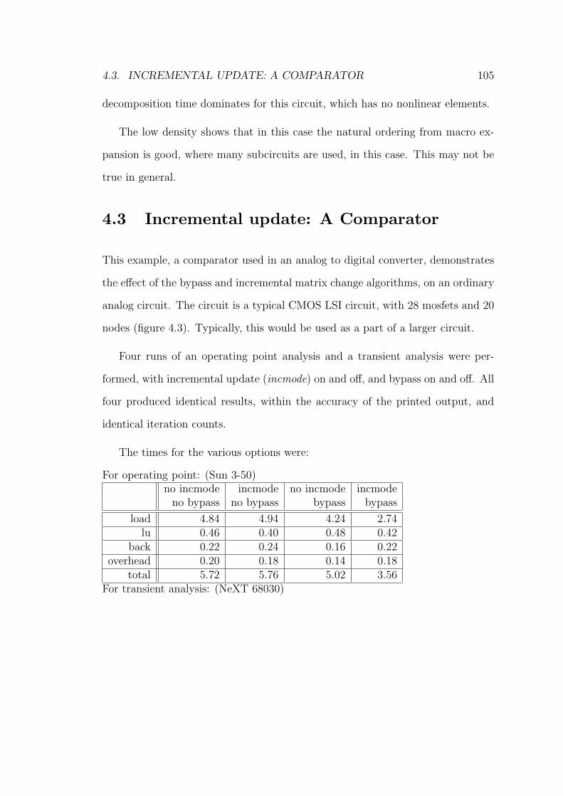
4.3. INCREMENTAL UPDATE: A COMPARATOR 105
decomposition time dominates for this circuit, which has no nonlinear elements.
The low density shows that in this case the natural ordering from macro ex-
pansion is good, where many subcircuits are used, in this case. This may not be
true in general.
4.3 Incremental update: A Comparator
This example, a comparator used in an analog to digital converter, demonstrates
the effect of the bypass and incremental matrix change algorithms, on an ordinary
analog circuit. The circuit is a typical CMOS LSI circuit, with 28 mosfets and 20
nodes (figure 4.3). Typically, this would be used as a part of a larger circuit.
Four runs of an operating point analysis and a transient analysis were per-
formed, with incremental update (incmode) on and off, and bypass on and off. All
four produced identical results, within the accuracy of the printed output, and
identical iteration counts.
The times for the various options were:
For operating point: (Sun 3-50)no incmode incmode no incmode incmode
no bypass no bypass bypass bypass
load 4.84 4.94 4.24 2.74lu 0.46 0.40 0.48 0.42
back 0.22 0.24 0.16 0.22overhead 0.20 0.18 0.14 0.18
total 5.72 5.76 5.02 3.56For transient analysis: (NeXT 68030)

4.3. INCREMENTAL UPDATE: A COMPARATOR 106
+ −
Vdd
M2
20 30
M1
20 30
M4
10 30
M3
100 5
1
67
0
+ −
+ −
Vip
Vip
M5
100 5
M7
100 7
M8
100
10M
1210
0 5
M9
200
10
M10
200
10
M6
10 30
M11
100 5
M13 10 30
1
2
811
3
12
9
0
7
10
+ −
+ −
Vcl
bV
cl
C1
2p
C2
2p
M24
200 5
M14 5 5
M20 10 5
M22
200 5
M23
200 5
M19 20 30
M18 20 30
M21 10 5
M15 5 5
1
1517
45
18
1314
9 12
0
7
M16 20 30
M25 20 30
M27 10 5
M28 5 5
M26 10 30
M17 20 30
1
15
17
0
16
19
20
Figure 4.3: A comparator circuit

4.4. MIXED-MODE SIMULATION: A STRING OF GATES 107
no incmode incmode no incmode incmodeno bypass no bypass bypass bypass
load 22.81 23.39 21.48 9.63lu 2.68 2.79 2.77 2.77
back 1.28 1.42 1.51 1.38overhead 1.58 1.15 1.43 1.07
total 28.35 28.75 27.19 14.85
From these figures, the lu, back, and overhead times are close to the same
for all options, as expected. The load time, which includes model evaluation, is
significantly different.
Incmode alone results in no time savings, because all calculations still need to
be made. In fact, there is a slight penalty. Bypass alone results in a small savings
of about 10%. Using both together results in much more than expected. Load
time is roughly cut in half.
The bypass mode causes model evaluation to be bypassed when the inputs are
within some tolerance on successive iterations. The process of model evaluation
includes solving some equations and activating a subcircuit, which loads its values
into the system of equations to be solved. When the matrix needs to be rebuilt
(no incmode) it is possible to bypass solving the model equations, but the values
must still be added to the matrix, causing the subcircuit to be activated. When
the matrix does not need to be rebuilt, there is no need to activate the subcircuit,
resulting in significant time savings.
4.4 Mixed-mode simulation: A string of gates

4.4. MIXED-MODE SIMULATION: A STRING OF GATES 108
U2 U3 U4
U5 U6 U7
V1
1 2 3 4
5 6 7
Figure 4.4: A string of inverters
M2100100
M1100100
Vdd=5
+
−
3
4
1
2
Figure 4.5: A CMOS inverter

4.4. MIXED-MODE SIMULATION: A STRING OF GATES 109
This example, a gate array, demonstrates a mixed analog and digital circuit. A low
frequency sinusoidal signal is applied to the input of a string of six logic inverters
(figures 4.4, 4.5). At some point the signal is clean enough to be processed as
digital. The circuit was run in all three modes, analog, mixed, and digital, with
a variety of input signals. As expected, the analog mode simulation gives good
accuracy with poor speed. The digital mode simulation gives poor results in cases
where the input is not a valid digital signal, but does it fast. The mixed mode
gives good results, with a speed in between. The circuit also demonstrates the
event driven step control, in digital and mixed mode.
In the first test, the input is a square wave, a valid logic signal, but from an
analog source. In the second test, the input is a large sinusoid (5 volts p-p). In
the third test, the input voltage is decreased, so the thresholds of the first gate
are never met.
0.12
Logic state: 3 = high 2 = falling 1 = rising 0 = low
Quality: 0 = proper logic signal1 = improving2 = improper: must use analog
Mode: 0 = gate in logic mode 1 = gate in analog mode 2 = analog elements
Figure 4.6: Logic display syntax
The output of the simulation is shown here in tabular form, with notes to show

4.4. MIXED-MODE SIMULATION: A STRING OF GATES 110
when mode switching occurs. A logic state is shown in the form a.bc, where a is
the state (3 = high, 2 = falling, 1 = rising, 0 = low), b is an indication of the
quality of the signal as digital (2 = bad, 1 = improving, 0 = good), and c indicates
which simulation mode was used (2 = always analog, 1 = gate as analog, 0 = gate
as digital). This is shown in figure 4.6.
* 6 inverters as gates* Specify the input signal.gen freq=1 offset=2.5 init=2.5 ampl=2.5** Circuit description, SPICE-like formatV1 1 0 generator( 1. )U2 0 2 1 mos invU3 0 3 2 mos invU4 0 4 3 mos invU5 0 5 4 mos invU6 0 6 5 mos invU7 0 7 6 mos inv** Description of the logic family.model mos logic ( delay= 1n rise= 1n fall= 1n rs= 100. rw= 1.G+ thh= 0.75 thl= 0.25 mr= 5. mf= 5. over=10k vmax= 5. vmin= 0. )** Circuit description of the analog equivalent of the logic inverter.subckt mosinv1 1 2 3M1 2 3 1 1 nmos l= 100.u w= 100.u nrd= 1. nrs= 1.M2 2 3 4 4 pmos l= 100.u w= 100.u nrd= 1. nrs= 1.Vdd 4 1 dc ( 5. ).ends** Description of the mosfet models used.model nmos nmos (level=2 vto= 0. gamma= 0. phi= 0.6 is= 10.E-15 pb= 0.8+ cgso= 0. cgdo= 0. cgbo= 0. rsh= 0. cj= 0. mj= 0.5 cjsw= 0. mjsw= 0.33+ tox= 100.n nfs= 0. tpg=1 ld= 0. uo= 600. neff= 1. fc= 0.5 delta= 0. )*+(* vfb=-0.6 * kp= 20.71886u ).model pmos pmos (level=2 vto= 0. gamma= 0. phi= 0.6 is= 10.E-15 pb= 0.8+ cgso= 0. cgdo= 0. cgbo= 0. rsh= 0. cj= 0. mj= 0.5 cjsw= 0. mjsw= 0.33+ tox= 100.n nfs= 0. tpg=1 ld= 0. uo= 600. neff= 1. fc= 0.5 delta= 0. )*+(* vfb=-0.6 * kp= 20.71886u )** Commands, what to do..options itl4=30 out=170.print tran v(nodes) l(nodes).tran 0 10 .05

4.4. MIXED-MODE SIMULATION: A STRING OF GATES 111
.end
4.4.1 Clean Digital Input
For the first test the input signal used is a square wave, a good digital signal. The
simulation starts in analog mode then switches. U2 and U3 switch at 1 second.
The other gates switch at 1.5 seconds. Since the signals are all clean, they remain
in digital mode once there. For other signals this will not be the case.
-->gen freq=0. ampl=1. max=5. min=0. offset=0. init=2.5-->gen rise=1.n fall=1.n width=0.5 period=1.-->set bypass incmode mixed-->tr 0 10 .1 skip 10Time v(1) v(4) v(7) logic(1) logic(4) logic(7)0. 2.5 2.3893 4.9847 1.22 1.21 3.110.1 5. 96.374p 5. 3.12 0.21 3.110.2 5. 96.374p 5. 3.12 0.21 3.110.3 5. 96.374p 5. 3.12 0.21 3.110.4 5. 96.374p 5. 3.12 0.21 3.110.5 5. 96.374p 5. 3.12 0.21 3.110.6 0. 5. 96.371p 0.02 3.11 0.010.7 0. 5. 96.371p 0.02 3.11 0.010.8 0. 5. 96.371p 0.02 3.11 0.010.9 0. 5. 96.371p 0.02 3.11 0.011. 0. 5. 96.371p 0.02 3.11 0.01
U2:98964 switch to digitalU3:98964 switch to digital1.1 5. 5. 96.371p 3.02 3.11 0.011.2 5. 5. 96.371p 3.02 3.11 0.011.3 5. 5. 96.371p 3.02 3.11 0.011.4 5. 5. 96.371p 3.02 3.11 0.011.5 5. 5. 96.371p 3.02 3.11 0.01
U4:99067 switch to digitalU5:99067 switch to digitalU6:99072 switch to digitalU7:99072 switch to digital1.6 0. 5. 0. 0.02 3. 0.1.7 0. 5. 0. 0.02 3. 0.1.8 0. 5. 0. 0.02 3. 0.
............

4.4. MIXED-MODE SIMULATION: A STRING OF GATES 112
The running time varied from 87.51 seconds to 14.95 seconds for the various
simulation options. The total time for mixed mode is only slightly slower than the
digital mode. There is a significant time savings by using bypass and incremental
matrix update. For all modes, the time spent solving the system of equations and
for overhead was about the same. In the digital and mixed cases they dominated.
This document discussed methods of speeding up the solution phase, but the
partial solution method is not implemented. Adding the partial solution method
will reduce the time spent in solving the equations for the digital and mixed cases.
analog analog mixed mixed digital digitalno inc incmode no inc incmode no inc incmode
no byp bypass no byp bypass no byp bypass
load 73.71 13.31 10.98 4.40 4.33 2.50lu 5.80 6.08 4.46 5.94 5.69 5.86
back 2.30 1.92 1.71 1.76 2.04 2.11output 3.89 3.87 3.27 3.27 3.11 3.09
overhead 1.81 1.82 1.56 1.41 1.53 1.39total 87.51 27.00 21.99 16.78 16.71 14.95
iterations 4570 4536 4508 4505 4496 4496
4.4.2 A Signal Too Slow
The second test uses a sinusoidal input, which is not a proper logic signal. This
signal has an adequate amplitude and it is properly offset, but the rise and fall
times are much too slow. The signal used is a 1 Hz sine wave, with a peak ampli-
tude of 2.5 volts, offset by 2.5 volts. The maximum voltage is 5, and the minimum
is 0, like a digital signal, but the transition is too slow. The proper behavior of
this circuit is for the signal to become increasingly square as it propagates. After

4.4. MIXED-MODE SIMULATION: A STRING OF GATES 113
several stages, the rise and fall times are fast enough to look like a proper digital
signal.
.generator freq=1 ampl=2.5 offset=2.5 init=2.5
The simulation starts, as usual, with all gates assumed to need analog simula-
tion. After 1 second (2 state transitions), the last two (U6 and U7) are observed
to be clean enough for digital simulation, but there it is questionable later at 1.1
and 1.6 seconds, when they hunt, and eventually settle to digital mode at 1.6 sec-
onds. At 1.1 seconds, U5 attempts, unsuccessfully, to switch to digital mode, then
switches to digital at 1.5 seconds, hunts at 2.1 seconds, then settles into digital
mode at 2.6 seconds. U4 attempts digital mode at 1.6 seconds, switches back to
analog, to remain there, at 2.1 seconds. There are no more mode changes after 2.6
seconds. For the remainder of the run, U2, U3, and U4 are simulated as analog,
and U5, U6, and U7 are simulated as digital. Some of the hunting may be due to
a mismatch between the analog and digital models in delay and transition time.
The reason for the hunting in this case, is that inconsistent values during
iterating the nonlinear model equations produce values that are out of range.
This suggests a need to not switch based on non-converged values. As presently
implemented, it will switch on any value, converged or not, for that iteration. On
later iterations it will switch to the proper mode. The cost is that it is in analog
mode more than necessary.
Mixed mode simulation with automatic switching:
-->set mixed

4.4. MIXED-MODE SIMULATION: A STRING OF GATES 114
-->print tran v 1 4 5 logic 1 4 5-->tr 0 10 .1 skip 10Time v(1) v(4) v(5) logic(1) logic(4) logic(5)0. 2.5 2.3893 3.4393 1.22 1.21 1.210.1 3.9695 370.07n 5. 3.12 0.21 3.110.2 4.8776 -45.656p 5. 3.12 0.21 3.110.3 4.8776 -45.656p 5. 3.12 0.21 3.110.4 3.9695 370.07n 5. 3.12 0.21 3.110.5 2.5 2.3893 3.4394 2.22 1.21 2.110.6 1.0305 5. -75.88p 0.12 3.11 0.010.7 0.12236 5. -75.938p 0.12 3.11 0.010.8 0.12236 5. -75.938p 0.12 3.11 0.010.9 1.0305 5. -75.88p 0.12 3.11 0.01
U6:532 switch to digitalU7:532 switch to digital1. 2.5 2.3894 3.4393 1.22 2.11 1.01
U5:541 switch to digitalU5:542 switch to analogU7:542 switch to analogU6:543 switch to analogU6:547 switch to digitalU7:547 switch to digital1.1 3.9695 370.07n 5. 3.12 0.11 3.011.2 4.8776 -45.55p 5. 3.12 0.11 3.011.3 4.8776 -45.55p 5. 3.12 0.11 3.011.4 3.9695 370.07n 5. 3.12 0.11 3.011.5 2.5 2.3893 3.4394 2.22 1.11 2.01
U4:818 switch to digitalU5:818 switch to digitalU4:819 switch to analogU5:819 switch to analogU4:822 switch to digitalU5:822 switch to digitalU7:822 switch to analogU6:823 switch to analogU7:823 switch to digitalU7:824 switch to analogU6:825 switch to digitalU7:825 switch to digital1.6 1.0305 5. 5. 0.12 3. 3.1.7 0.12236 5. 5. 0.12 3. 3.1.8 0.12236 5. 5. 0.12 3. 3.1.9 1.0305 5. 5. 0.12 3. 3.2. 2.5 5. 5. 1.22 3. 3.
U4:1075 switch to analogU5:1076 switch to analog2.1 3.9695 370.07n 5. 3.12 0.11 3.012.2 4.8776 -45.661p 5. 3.12 0.11 3.012.3 4.8776 -45.661p 5. 3.12 0.11 3.01

4.4. MIXED-MODE SIMULATION: A STRING OF GATES 115
2.4 3.9695 370.07n 5. 3.12 0.11 3.012.5 2.5 2.3893 3.4395 2.22 1.11 2.01
U5:1342 switch to digital2.6 1.0305 5. 0. 0.12 3.01 0.2.7 0.12236 5. 0. 0.12 3.01 0.2.8 0.12236 5. 0. 0.12 3.01 0.2.9 1.0305 5. 0. 0.12 3.01 0.3. 2.5 2.3894 0. 1.22 2.01 0.3.1 3.9695 370.07n 5. 3.12 0.01 3.
................8.9 1.0305 5. 0. 0.12 3.01 0.9. 2.5 2.3894 0. 1.22 2.01 0.9.1 3.9695 370.07n 5. 3.12 0.01 3.9.2 4.8776 96.376p 5. 3.12 0.01 3.9.3 4.8776 96.376p 5. 3.12 0.01 3.9.4 3.9695 370.07n 5. 3.12 0.01 3.9.5 2.5 2.3893 5. 2.22 1.01 3.9.6 1.0305 5. 0. 0.12 3.01 0.9.7 0.12236 5. 0. 0.12 3.01 0.9.8 0.12236 5. 0. 0.12 3.01 0.9.9 1.0305 5. 0. 0.12 3.01 0.10. 2.5 2.3894 0. 1.22 2.01 0.
The analog simulation shows identical logic states for the gates simulated as
digital. The voltages are nearly the same except for the obvious lack of precision
in digital mode. The most obvious is the in-transition state (at 3, 9, 9.5, and 10
seconds in the range shown). The voltage at node 5 is 3.43 (obviously in transition)
in the analog simulation. The digital simulation shows it as either 0 or 5, showing
a mismatch between the digital and analog models in delay and transition time.
In all these cases, the logic state shows rising or falling. Considering that in this
example the transition times are fast compared to the displayed step sizes, this is
not surprising.
Full analog simulation:
-->set analog-->tr 0 10 .1 skip 10Time v(1) v(4) v(5) logic(1) logic(4) logic(5)

4.4. MIXED-MODE SIMULATION: A STRING OF GATES 116
.......1.8 0.12236 5. -76.06p 0.12 3.01 0.011.9 1.0305 5. -76.001p 0.12 3.01 0.012. 2.5 2.3894 3.4393 1.22 2.01 1.012.1 3.9695 370.07n 5. 3.12 0.01 3.012.2 4.8776 -45.653p 5. 3.12 0.01 3.012.3 4.8776 -45.653p 5. 3.12 0.01 3.012.4 3.9695 370.07n 5. 3.12 0.01 3.012.5 2.5 2.3893 3.4395 2.22 1.01 2.012.6 1.0305 5. -75.998p 0.12 3.01 0.012.7 0.12236 5. -76.057p 0.12 3.01 0.012.8 0.12236 5. -76.057p 0.12 3.01 0.012.9 1.0305 5. -75.998p 0.12 3.01 0.013. 2.5 2.3894 3.4392 1.22 2.01 1.013.1 3.9695 370.07n 5. 3.12 0.01 3.01
............8.9 1.0305 5. -75.988p 0.12 3.01 0.019. 2.5 2.3894 3.4391 1.22 2.01 1.019.1 3.9695 370.07n 5. 3.12 0.01 3.019.2 4.8776 -45.64p 5. 3.12 0.01 3.019.3 4.8776 -45.64p 5. 3.12 0.01 3.019.4 3.9695 370.07n 5. 3.12 0.01 3.019.5 2.5 2.3893 3.4396 2.22 1.01 2.019.6 1.0305 5. -75.99p 0.12 3.01 0.019.7 0.12236 5. -76.048p 0.12 3.01 0.019.8 0.12236 5. -76.048p 0.12 3.01 0.019.9 1.0305 5. -75.99p 0.12 3.01 0.0110. 2.5 2.3894 3.4391 1.22 2.01 1.01
The full digital simulation appears to be valid, except that the transition
states are not shown. The transitions occur at times other than those displayed,
indicating the time at which transitions occurred was not modelled correctly.
Considering the coarseness of this printout, it is probably accurate enough, but in
practice it may not be. The fact that the results appear to be correct, but in fact
are not, points out an important problem that implicit mixed mode simulation
helps to solve.
Full digital simulation:
-->set digital-->tr 0 10 .1 skip 10

4.4. MIXED-MODE SIMULATION: A STRING OF GATES 117
Time v(1) v(4) v(5) logic(1) logic(4) logic(5)0. 2.5 0. 0. 1.22 1.2 1.20.1 3.9695 0. 5. 3.12 0. 3.0.2 4.8776 0. 5. 3.12 0. 3.0.3 4.8776 0. 5. 3.12 0. 3.0.4 3.9695 0. 5. 3.12 0. 3.0.5 2.5 0. 5. 2.22 0. 3.0.6 1.0305 5. 0. 0.12 3. 0.0.7 0.12236 5. 0. 0.12 3. 0.
.................8.8 0.12236 5. 0. 0.12 3. 0.8.9 1.0305 5. 0. 0.12 3. 0.9. 2.5 5. 0. 1.22 3. 0.9.1 3.9695 0. 5. 3.12 0. 3.9.2 4.8776 0. 5. 3.12 0. 3.9.3 4.8776 0. 5. 3.12 0. 3.9.4 3.9695 0. 5. 3.12 0. 3.9.5 2.5 0. 5. 2.22 0. 3.9.6 1.0305 5. 0. 0.12 3. 0.9.7 0.12236 5. 0. 0.12 3. 0.9.8 0.12236 5. 0. 0.12 3. 0.9.9 1.0305 5. 0. 0.12 3. 0.10. 2.5 5. 0. 1.22 3. 0.
A closer look near the transition at 9.5 seconds reveals the importance of this
difference. The mixed simulation, with the first few gates simulated in analog
mode, correctly shows the state change at node 5 as occurring at 9.5 seconds.
The full digital simulation shows the transition delayed until 9.59 seconds. The
difference is due to the apparent time of transition of the input. With the first
gate simulated as analog, the signal is amplified before making any state decisions,
so the transition point of the entire circuit is at the midpoint, about 2.5 volts.
With the first gate simulated as digital, the state transition occurs when the input
signal passes from the transition region to the logic-low region, near 1.16 volts.
This state change time is propagated to the rest of the circuit. This would be the
result with other “mixed-mode” simulators.

4.4. MIXED-MODE SIMULATION: A STRING OF GATES 118
More detail around 9.5 seconds, mixed mode:
Time v(1) v(4) v(5) logic(1) logic(4) logic(5)9.4 3.9695 370.07n 5. 3.12 0.01 3.9.4 3.9695 370.07n 5. 3.12 0.01 3.9.41 3.8396 1.1411u 5. 3.12 0.01 3.9.42 3.7044 3.3673u 5. 2.12 0.01 3.9.43 3.5644 9.6149u 5. 2.22 0.01 3.9.44 3.4203 26.904u 5. 2.22 0.01 3.9.45 3.2725 74.869u 5. 2.22 0.01 3.9.46 3.1217 211.35u 5. 2.22 0.01 3.9.47 2.9685 624.3u 5. 2.22 0.01 3.9.48 2.8133 0.0020482 5. 2.22 0.01 3.9.49 2.657 0.0087765 5. 2.22 0.01 3.9.5 2.5 2.3893 5. 2.22 1.01 3.9.5 2.5 2.3893 5. 2.22 1.01 3.9.51 2.343 4.9912 5. 2.22 3.01 2.9.51 2.343 4.9912 0. 2.22 3.01 0.9.51 2.343 4.9912 0. 2.22 3.01 0.9.51 2.343 4.9912 0. 2.22 3.01 0.9.52 2.1867 4.998 0. 2.22 3.01 0.9.53 2.0315 4.9994 0. 2.22 3.01 0.9.54 1.8783 4.9998 0. 2.22 3.01 0.9.55 1.7275 4.9999 0. 2.22 3.01 0.9.56 1.5797 5. 0. 2.22 3.01 0.9.57 1.4356 5. 0. 2.22 3.01 0.9.58 1.2956 5. 0. 2.22 3.01 0.9.59 1.1604 5. 0. 0.12 3.01 0.9.6 1.0305 5. 0. 0.12 3.01 0.
More detail around 9.5 seconds, digital mode:
Time v(1) v(4) v(5) logic(1) logic(4) logic(5)9.4 3.9695 0. 5. 3.12 0. 3.9.4 3.9695 0. 5. 3.12 0. 3.9.41 3.8396 0. 5. 3.12 0. 3.9.42 3.7044 0. 5. 2.12 0. 3.9.43 3.5644 0. 5. 2.22 0. 3.9.44 3.4203 0. 5. 2.22 0. 3.9.45 3.2725 0. 5. 2.22 0. 3.9.46 3.1217 0. 5. 2.22 0. 3.9.47 2.9685 0. 5. 2.22 0. 3.9.48 2.8133 0. 5. 2.22 0. 3.9.49 2.657 0. 5. 2.22 0. 3.9.5 2.5 0. 5. 2.22 0. 3.9.5 2.5 0. 5. 2.22 0. 3.9.51 2.343 0. 5. 2.22 0. 3.9.52 2.1867 0. 5. 2.22 0. 3.

4.4. MIXED-MODE SIMULATION: A STRING OF GATES 119
9.53 2.0315 0. 5. 2.22 0. 3.9.54 1.8783 0. 5. 2.22 0. 3.9.55 1.7275 0. 5. 2.22 0. 3.9.56 1.5797 0. 5. 2.22 0. 3.9.57 1.4356 0. 5. 2.22 0. 3.9.58 1.2956 0. 5. 2.22 0. 3.9.59 1.1604 0. 5. 0.12 0. 3.9.59 1.1604 0. 5. 0.12 0. 3.9.59 1.1604 0. 5. 0.12 1. 3.9.59 1.1604 5. 5. 0.12 3. 2.9.59 1.1604 5. 0. 0.12 3. 0.9.59 1.1604 5. 0. 0.12 3. 0.9.59 1.1604 5. 0. 0.12 3. 0.9.6 1.0305 5. 0. 0.12 3. 0.
The simulation runs much slower with this input. There were roughly twice as
many iterations, hence twice the running time. The all digital mode runs in about
the same time as it did with the digital input, but in this case (slow sine input)
it gives questionable results. There is less difference between the full analog and
mixed simulations because several gates were in analog mode more of the time.
Again, the combined bypass and incremental update saved a significant amount of
time. The savings from bypass and incremental mode are more than the savings
from mixed-mode.
analog analog mixed mixed digital digitalno inc incmode no inc incmode no inc incmode
no byp bypass no byp bypass no byp bypass
load 148.51 65.12 83.82 50.25 4.53 2.61lu 11.46 11.36 11.13 11.25 5.41 5.92
back 4.51 4.06 4.03 4.01 1.88 1.67output 3.91 3.99 3.57 3.58 3.20 3.26
overhead 3.22 3.02 3.45 2.88 1.83 1.75total 171.60 87.56 105.99 71.97 16.85 15.21
iterations 9242 9192 9182 9136 4506 4506

4.4. MIXED-MODE SIMULATION: A STRING OF GATES 120
4.4.3 Input Signal Too Small
The third input signal used is a low amplitude sinusoid. The signal used here is,
again, 1 Hz with an offset of 2.5 volts, but the peak amplitude is only 1 volt. The
maximum voltage is 3.5 and the minimum is 1.5. It never leaves the transition
region. The proper behavior for this circuit is similar to the second case except
that it will take probably one more stage to become square enough. The simula-
tion results are very different between full digital and mixed mode. The digital
simulation is completely incorrect because it never senses any transitions.
The mode switching hunts more, because more of the simulation is analog, and
it is more likely that non-converged values are not appropriate for logic simulation.
The output results are as expected, for this circuit.
-->pr tran v 1 5 6 logic 1 5 6-->set mixed-->tr 0 10 .1 skip 10Time v(1) v(5) v(6) logic(1) logic(5) logic(6)..................7.8 1.5489 -46.309p 5. 1.22 0.01 3.7.9 1.9122 7.1127n 5. 1.22 0.01 3.
U7:41150 switch to analogU6:41151 switch to analogU7:41151 switch to digitalU6:41152 switch to digitalU7:41153 switch to analogU6:41154 switch to analogU7:41154 switch to digitalU6:41155 switch to digital8. 2.5 3.4761 0. 1.22 1.01 0.
U7:41156 switch to analogU6:41157 switch to analogU7:41157 switch to digitalU6:41158 switch to digitalU5:41159 switch to digitalU5:41160 switch to analogU7:41161 switch to analog
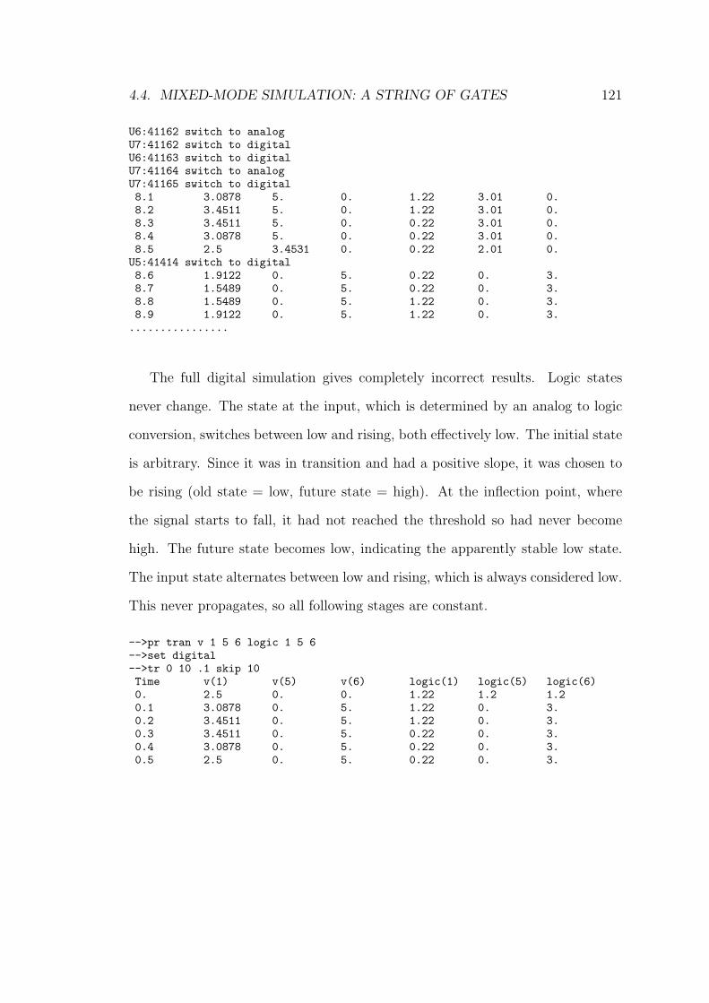
4.4. MIXED-MODE SIMULATION: A STRING OF GATES 121
U6:41162 switch to analogU7:41162 switch to digitalU6:41163 switch to digitalU7:41164 switch to analogU7:41165 switch to digital8.1 3.0878 5. 0. 1.22 3.01 0.8.2 3.4511 5. 0. 1.22 3.01 0.8.3 3.4511 5. 0. 0.22 3.01 0.8.4 3.0878 5. 0. 0.22 3.01 0.8.5 2.5 3.4531 0. 0.22 2.01 0.
U5:41414 switch to digital8.6 1.9122 0. 5. 0.22 0. 3.8.7 1.5489 0. 5. 0.22 0. 3.8.8 1.5489 0. 5. 1.22 0. 3.8.9 1.9122 0. 5. 1.22 0. 3.
................
The full digital simulation gives completely incorrect results. Logic states
never change. The state at the input, which is determined by an analog to logic
conversion, switches between low and rising, both effectively low. The initial state
is arbitrary. Since it was in transition and had a positive slope, it was chosen to
be rising (old state = low, future state = high). At the inflection point, where
the signal starts to fall, it had not reached the threshold so had never become
high. The future state becomes low, indicating the apparently stable low state.
The input state alternates between low and rising, which is always considered low.
This never propagates, so all following stages are constant.
-->pr tran v 1 5 6 logic 1 5 6-->set digital-->tr 0 10 .1 skip 10Time v(1) v(5) v(6) logic(1) logic(5) logic(6)0. 2.5 0. 0. 1.22 1.2 1.20.1 3.0878 0. 5. 1.22 0. 3.0.2 3.4511 0. 5. 1.22 0. 3.0.3 3.4511 0. 5. 0.22 0. 3.0.4 3.0878 0. 5. 0.22 0. 3.0.5 2.5 0. 5. 0.22 0. 3.

4.4. MIXED-MODE SIMULATION: A STRING OF GATES 122
..................7.8 1.5489 0. 5. 1.22 0. 3.7.9 1.9122 0. 5. 1.22 0. 3.8. 2.5 0. 5. 1.22 0. 3.8.1 3.0878 0. 5. 1.22 0. 3.8.2 3.4511 0. 5. 1.22 0. 3.8.3 3.4511 0. 5. 0.22 0. 3.8.4 3.0878 0. 5. 0.22 0. 3.8.5 2.5 0. 5. 0.22 0. 3.8.6 1.9122 0. 5. 0.22 0. 3.8.7 1.5489 0. 5. 0.22 0. 3.8.8 1.5489 0. 5. 1.22 0. 3.8.9 1.9122 0. 5. 1.22 0. 3.
................
4.4.4 Summary
This example has shown the application of implicit mixed-mode simulation to a
simple inverter string, with a variety of inputs. For the clean, digital input, the
running time was about a factor of six faster than traditional analog simulation,
and only slightly slower than the fully digital mode. The load time, including
model evaluation, was faster than traditional by about a factor of 20. For a
slowly changing sinusoidal input, only a slight saving was realized, but it produced
correct results in all cases. Sometimes, the fully digital mode did not.
The time savings from incremental update of the matrix, combined with model
evaluation bypass, was significant, a factor of two or three in total running time,
two to five in load time, including model evaluation. One conclusion that can be
drawn from this is that it is necessary to switch modes.

Chapter 5
Contributions and Suggestionsfor Further Research
In this dissertation some techniques have been presented to combine different
simulation modes implicitly, without direct instructions from the user.
Modifications to the well-known LU decomposition algorithms to allow for the
solution of a partial matrix were presented. This allows parts of the matrix to
be bypassed, or totally ignored, if the information that part solves for is known
by some other means. It provides a more efficient means of simulating parts
of the circuit, by applying the selective trace algorithm, which is common in
digital simulators, to the entire circuit. Parts of circuits with widely varying time
constants, and very different signal frequencies can be simulated together without
interfering with each other.
A method was presented to automatically choose between logic and analog
simulation in parts of the circuit that have a logic level description. The choice
123

124
is based on the assumption that when the digital signals appear to be clean, a
digital simulation is valid. When the digital signals show race and spike conditions
or slow transition times, they are suspect and analog simulation is used for the
problem parts of the circuit. The change can be made on parts of the circuit
as small as a single gate. When the conversion between modes is poorly defined
and difficult to make, the analog mode is selected. Since the problem parts of
the circuit are simulated as analog at the remaining interface points, the signal is
hopefully clean, and the conversion can be made easily and unambiguously.
The implementation used here begins in the analog mode to establish the initial
conditions. When a signal passes two transitions, while all the time meeting the
criteria for a proper digital signal, it is accepted as digital. Any hint at failing to
meet the criteria causes a switch back to analog mode. The method used is prone
to hunting problems, where a gate switched back and forth between analog and
digital mode repeatedly, in marginal cases. This is not a serious problem for a
user, because the run time is no worse than analog simulation, and the accuracy
is no worse than digital simulation. Usually, when hunting, it is mostly in digital
mode, so the effect of the hunting is that simulation time is increased somewhat
over what it would be without the hunting problem.
For analog circuits model bypass is used to eliminate needless calculations after
a the terminal voltages of a subcircuit or device have converged, but other parts of
the circuit have not. Bypass is not new. It results in about 10% savings in time,
with no apparent loss of accuracy, and usually no increase in iteration count.

125
Instead of rebuilding the matrix at each iteration, URECA keeps the old ma-
trix and updates it, usually by adding the difference between the new and old
values. Without bypass this would have no benefit. When a model or subcircuit
is bypassed it is not necessary to load the values into the matrix. If an entire
subcircuit or semiconductor device can be bypassed, it eliminates the need to
process the subcircuit at all, resulting in considerable time savings. Tests have
shown that model evaluation and matrix load time are cut in half, or better, for
moderate sized semiconductor circuits. Up to five times improvement has been
demonstrated. This is expected to improve for very large circuits.
The use of selective trace to control model evaluation in analog simulation was
investigated, but not implemented. The success of the incremental update method
indicates that selective trace should also be successful. The most important benefit
of selective trace is believed to be that it is possible to activate small parts of the
circuit without activating the main circuit. This should improve simulation time
considerably for circuits with widely differing frequencies of operation, such as
sampled data circuits.
A vector method for solving the matrix was reviewed and implemented. It is a
nearly optimal method for LU decomposition of the particular type of sparse ma-
trix that exists in circuit simulation of large circuits. It was shown to be effective
in solving large circuits, those of over 1000 nodes. For typical semiconductor cir-
cuits matrix solution time is small compared to model evaluation time. For digital
circuits in digital mode, matrix solution still dominates. A theoretical analysis

126
was done on methods of solving part of the matrix, but this was not implemented.
The unnecessary matrix solution is the one factor in why even the digital mode is
not nearly as fast as a pure logic simulator.
In this work, it became apparent that some areas merit further investigation:
Cached evaluation of subcircuits and models. Large circuits tend to have
many blocks and devices repeated. Often their operating points are close, so
they also can be considered to be repeated. Existing simulators evaluate the
models every time. Since model evaluation time is dominant, considerable
time could be saved if they could re-use the results of model evaluation, by
saving them in a cache.
Cleaner switching between analog and digital modes. During iteration,
the apparent voltages at some nodes of an analog circuit can take on im-
proper values. After a few iterations of Newton’s method, they settle to a
reasonable value. If the node in question drives a digital element, this appar-
ent voltage swing during iteration can temporarily trick the mode switching
to switch back to analog, even though the converged signal is proper for dig-
ital simulation. This switching only affects a few iterations then it switches
back to digital mode, so it does not hurt the accuracy. The user may not
even notice it unless notification of switching was requested. The problem
with it is that it wastes time by activating the analog model for a few it-
erations, when it will switch back to digital before iteration is complete.
An investigation is needed to determine when it is acceptable to ignore the

127
fact that a signal was marked as invalid, and thus continue with digital
simulation.
Further analysis and testing of the selective trace method. In this work,
the application of selective trace to analog simulation was investigated theo-
retically, but not fully implemented. The implementation activates the main
circuit on all events. By using selective trace, a subcircuit could be activated
without the main circuit, resulting in a large time savings for large circuits
where parts of the circuit require smaller time steps than the main circuit,
such as sampled data systems.
Partial solutions. Techniques were described here to do a partial LU decompo-
sition of a matrix in which only a few elements have changed. The same
techniques can be used to solve for a few node voltages without solving for
all of them. Work needs to be done on how to determine which elements
need updating, taking into account how the changes propagate. It is im-
portant that the method for deciding be efficient, otherwise its cost may
mask the savings. A study is also needed on how this effects the integration
algorithms for capacitors and inductors, since the voltages available are not
all at the same time. It is probable that the voltages at the two terminals of
a capacitor are at different times, and the previous time values at another
set of different times, with different differences.
Improvement of memory utilization. The combined methods in this work
were not optimized. They use more space than traditional simulation, in
128
all areas. With large circuits, the space consideration is important, at least
to minimize swapping. There are many areas with redundant storage, such
as duplication of subcircuits. The storage for identical subcircuits could be
shared. In addition to saving space, it would help with cached evaluation of
models.
Analysis of error accumulation in matrix updates. In this work matrices
are updated often by adding a difference between a new and old value. Each
time there is probably some small round-off error. Often, during iteration
when far from convergence, the round off errors can be very large. These
errors can accumulate as partial solutions are repeated. It was assumed,
possibly incorrectly, that these errors are small. The present implementa-
tion of URECA senses certain conditions where these errors are large, and
rebuilds the entire matrix. Work needs to be done to develop a more efficient
scheme.
Integration of other methods to the scheme. The methods used here are
traditional circuit simulation, and logic simulation. There are other methods
in use, including harmonic balance and analog behavioral modeling. These
could be integrated into the scheme, for a true multi-mode simulator.
AC analysis of a mixed mode circuit. In traditional simulators, the AC anal-
ysis uses a linearized model based on the DC or transient analysis. Some-
times, the AC performance is desired for a mixed mode circuit. An example
is a sampled data filter (digital or switched capacitor): analog in, sample,

129
process the samples, convert back to the same analog domain. What is the
frequency response of this “filter”? Another example is an RF communica-
tion channel: audio in, modulate, send through channel, demodulate, audio
out. One way is to do a mixed-mode transient analysis, and FFT to get the
frequency domain information, but this is inefficient. Similarly, pole-zero
analysis of a mixed mode circuit would be desirable.
Implementing on non-traditional computers. With VLSI, non-traditional
computer architectures are becoming practical and affordable. Massively
parallel architectures, such as the Connection Machine, could become popu-
lar, and migrate from being purely research machines to the workstations. A
study of mixed-mode simulation on these new computer architectures could
be productive.
Detailed simulation of devices. The two modes in this simulator are actually
different levels of detail. One level (circuit level) decomposes elements into
smaller parts. The other level (logic or abstract level) approximates them
by simple equations. One could consider the existing device models to be an
abstraction of a true device simulation. A full device simulation could then
be substituted for the models now used. This, of course, would increase
the simulation cost, but could provide information which is not presently
available.
Thermal analysis, with self-heating Thermal problems have always plagued
circuit designers. Usually thermal problem are dealt with in an ad-hoc

130
manner. Integrating a thermal analysis with the circuit analysis could point
out places where the circuit has thermal problems, and show if temperature
compensation techniques actually work.
Extraction of logic level parameters from the circuit model. The mixed-
mode simulation can use either a logic level or circuit level model for logic
elements. In the existing implementation, the logic parameters, and equiv-
alent circuit, are specified by the user, with no check that they match. This
inconsistency is one reason sometimes the mode selection mechanism hunts
between modes. It is possible to extract the logic parameters by simulating
the circuit model, or extract the values for a standard circuit model from
the logic model. This would both make it easier for the user and establish
some consistency between the two models.
In summary, the techniques described here allow simulation of mixed analog
and digital circuits with the analog and digital elements to be freely mixed, not
necessarily by the rules. The techniques here model the interface better than other
approaches.

Bibliography
[1] P. Antognetti and G. Massobrio, eds., Semiconductor Device Modeling
with SPICE, McGraw-Hill, 1988.
[2] H. A. Antosiewicz, Newton’s method and boundary value problems, Journal
of Computer Systems Science, 2 (1968), pp. 177–202.
[3] G. Arnout and H. deMan, The use of boolean controlled elements for
macro-modeling of digital circuits, in IEEE Proc. 1978 International Sympo-
sium on Circuits and Systems, IEEE, May 1978, pp. 522–526.
[4] , The use of threshold functions and boolean-controlled network elements
for macromodeling of LSI circuits, IEEE Journal of Solid State Circuits, SC-
13 (1978), pp. 326–332.
[5] R. C. Baldwin, An approach to the simulation of computer logic, in AIEE
Conference, 1959.
[6] A. K. Bose and S. A. Szygenda, Detection of static and dynamic hazards
in logic nets, in Proceedings of the 14th Design Automation Conference,
IEEE, ACM, IEEE, 1977, pp. 220–224.
131

BIBLIOGRAPHY 132
[7] R. K. Brayton, F. G. Gustavson, and G. D. Hachtel, A new efficient
algorithm for solving differential-algebraic systems using implicit backward
differentiation formulas, Proceedings of the IEEE, 60 (1972), pp. 98–108.
[8] B. R. Chawla, H. K. Gummel, and P. Kozak, MOTIS – an MOS tim-
ing simulator, IEEE Transactions on Circuits and Systems, CAS-22 (1975),
pp. 901–910.
[9] A. T. Davis, A vector approach to sparse nodal admittance matrices, in 30th
Midwest Symposium on Circuits and Systems, Aug. 1987.
[10] , Numerical methods for stiff differential equations, tech. rep., University
of Rochester, Rochester, NY, Apr. 1988.
[11] H. deMan, Mixed-mode simulation for MOS-VLSI: why, where, and how?,
in IEEE Proc. 1982 International Symposium on Circuits and Systems, IEEE,
May 1982, pp. 699–701.
[12] H. deMan, G. Arnout, and P. Reynaert, Mixed-mode circuit simu-
lation techniques and their implementation in DIANA, in Computer Design
Aids for VLSI Circuits, P. Antognetti, D. O. Pederson, and H. de Man, eds.,
Martinus Nijhoff Publishers, Dordrecht, The Netherlands, 1980.
[13] H. deMan and A. R. Newton, Hybrid simulation, in IEEE Proc. 1979
International Symposium on Circuits and Systems, IEEE, May 1979, pp. 249–
252.

BIBLIOGRAPHY 133
[14] H. deMan, J. Rabaey, G. Arnout, and J. Vandewalle, DIANA as
a mixed-mode simulator for mos lsi sampled-data circuits, in IEEE Proc.
1980 International Symposium on Circuits and Systems, IEEE, May 1980,
pp. 435–438.
[15] , Practical implementation of a general computer aided design technique
for switched capacitor circuits, IEEE J. Solid-State Circuits, SC-15 (1980),
pp. 190–200.
[16] J. J. Dongarra, F. G. Gustavson, and A. Karp, Implementing linear
algebra algorithms for dense matrices on a vector pipeline machine, SIAM
Review, 26 (1984), pp. 91–112.
[17] I. S. Duff, A survey of sparse matrix research, Proceedings of the IEEE, 65
(1977), pp. 500–535.
[18] E. B. Eichelberger, Hazard detection in combinational and sequential
switching circuits, in IBM Journal of Research and Development, IBM, Mar.
1965.
[19] S. P. Fan, M. Y. Hsueh, A. R. Newton, and D. O. Pederson,
MOTIS-C: A new circuit simulator for MOS LSI circuits, in Proc. IEEE
ISCAS, 1977, pp. 700–703.
[20] C. W. Gear, Numerical Initial Value Problems in Ordinary Differential
Equations, Prentice-Hall, Englewood Cliffs, New Jersey, 1971.
BIBLIOGRAPHY 134
[21] A. George, On block elimination for sparse linear systems, SIAM Journal
of Numerical Analysis, 11 (1974), pp. 585–603.
[22] P. E. Gill, W. Murray, M. A. Saunders, and M. H. Wright, Main-
taining LU factors of a general sparse matrix, Linear Algebra and its Appli-
cations, (1987), pp. 239–270.
[23] G. D. Hachtel, R. K. Brayton, and F. G. Gustavson, The sparse
tableau approach to network analysis and design, IEEE Transactions on Cir-
cuit Theory, CT-18 (1971), pp. 101–118.
[24] C. W. Ho, A. E. Ruehli, and P. A. Brennan, The modified nodal
approach to network analysis, IEEE Transactions on Circuits and Systems,
CAS-22 (1975), pp. 504–509.
[25] J. E. Kleckner, Advanced mixed-mode simulation techniques, ph.d. thesis,
University of California, Berkeley, 1984.
[26] E. S. Kuh and R. A. Rohrer, The state variable approach to network
analysis, Proceedings of the IEEE, 53 (1965), pp. 672–686.
[27] K. S. Kundert, Sparse matrix techniques, in Circuit Analysis, Simulation
and Design, Vol. 1, A. E. Ruehli, ed., Amsterdam, The Netherlands, 1986,
Elsevier Science Publishers B.V., pp. 281–324.

BIBLIOGRAPHY 135
[28] H. A. Mantooth, A summary of mixed analog-digital simulation, SRC
Technical Report T87109, Georgia Institute of Technology, Atlanta, Georgia
30332, Oct. 1987.
[29] H. M. Markowitz, The elimination form of the inverse and its application
to linear programming, Management Science, 3 (1957), pp. 255–269.
[30] W. J. McCalla, Fundamantals of Computer-Aided Circuit Simulation,
Kluwer Academic Publishers, Boston, 1988.
[31] L. W. Nagel, SPICE2: A computer program to simulate semiconductor
circuits, Memorandum ERL-M520, University of California, Berkeley, May
1975.
[32] A. R. Newton, The simulation of large-scale integrated circuits, Tech. Rep.
UCB/ERL M78/52, University of California, Berkeley, July 1978.
[33] , Techniques for the simulation of large-scale integrated circuits, IEEE
Transactions on Circuits and Systems, CAS-26 (1979), pp. 741–749.
[34] P. Odryna and S. Nassif, The ADEPT timing simulation algorithm, De-
sign Automation Guide, (1987), pp. 56–64.
[35] A. V. Oppenheim and R. W. Schafer, Digital Signal Processing,
Prentice-Hall, Englewood Cliffs, New Jersey, 1975.
[36] J. M. Ortega and W. C. Rheinbolt, Iterative Solution of Nonlinear
Equations in Several Variables, Academic Press, San Diego, 1970.

BIBLIOGRAPHY 136
[37] W. H. Press, B. P. Flannery, S. A. Teukolsky, and W. T. Vet-
terling, Numerical Recipes, Cambridge University Press, Cambridge, 1986.
[38] T. L. Quarles, Analysis of performance and convergence issues for cir-
cuit simulation, Ph.D. Thesis UCB/ERL M89/42, University of California,
Berkeley, 1989.
[39] N. B. G. Rabbat, A. L. Sangiovanni-Vincentelli, and H. Y. Hsieh,
A multilevel Newton algorithm with macromodeling and latency for the anal-
ysis of large-scale nonlinear circuits in the time domain, IEEE Transactions
on Circuits and Systems, CAS-26 (1979), pp. 733–741.
[40] V. B. Rao, D. V. Overhauser, T. N. Trick, and I. N. Hajj, Switch-
Level Timing Simulation of MOS VLSI Circuits, Kluwer Academic Publish-
ers, Boston, 1989.
[41] K. A. Sakallah, Mixed simulation of electronic integrated circuits, Re-
search Report CMUCAD-83-10, Carnegie-Mellon University, May 1983.
[42] K. A. Sakallah and S. W. Director, SAMSON2: An event driven
VLSI circuit simulator, Research Report CMUCAD-84-37, Carnegie-Mellon
University, Sept. 1984.
[43] , SAMSON2: An event driven VLSI circuit simulator, IEEE Transac-
tions on Computer-Aided Design, CAD-4 (1985), pp. 668–684.
BIBLIOGRAPHY 137
[44] R. A. Saleh, Iterated timing analysis and SPLICE1, Tech. Rep. UCB/ERL
M84/2, University of California, Berkeley, Jan. 1984.
[45] Silicon Compiler Systems, LSIM Users Guide, June 1987.
[46] W. D. Stanley, Network Analysis with Applications, Reston Publishing
Company, Reston, Virginia, 1985.
[47] D. V. Steward, On an approach to techniques for the analysis of the struc-
ture of large systems of equations, SIAM Review, 4 (1962), pp. 321–342.
[48] J. Stoer and R. Bulirsch, Introduction to Numerical Analysis, Springer-
Verlag, New York, 1980.
[49] G. Strang, Linear Algebra and its Applications, Academic Press, New York,
2 ed., 1976.
[50] J. A. Svoboda, Using nullors to analyse linear networks, International Jour-
nal on Circuit Theory and Applications, 14 (1986), pp. 169–180.
[51] S. A. Szygenda, TEGAS 2 - anatomy of a general purpose test genera-
tion and simulation system for digital logic, in Proc. 9th ACM-IEEE Design
Automation Workshop, ACM-IEEE, June 1972, pp. 116–127.
[52] J. Traub, Iterative Methods for the Solution of Equations, Prentice Hall,
Englewood Cliffs, New Jersey, 1964.
[53] E. G. Ulrich, Exclusive simulation of activity in digital networks, C. ACM,
12 (1969), pp. 102–110.

BIBLIOGRAPHY 138
[54] W. M. G. van Bokhoven, Linear implicit differentiation formulas of vari-
able step and order, IEEE Transactions on Circuits and Systems, CAS-22
(1975), pp. 109–115.
[55] M. E. van Valkenburg, Network Analysis, Prentice Hall, Englewood
Cliffs, New Jersey, 1974.
[56] R. Varga, Matrix Iterative Analysis, Prentice Hall, Englewood Cliffs, New
Jersey, 1962.
[57] J. Vlach and K. Singhal, Computer Methods for Circuit Analysis and
Design, Van Nostrand Reinhold Company, New York, 1983.
[58] J. K. White and A. Sangiovanni-Vincentelli, Relaxation Techniques
for the Simulation of VLSI Circuits, Kluwer Academic Publishers, Boston,
1987.