improvement of stopband performance in parallel …orbit.dtu.dk/files/4393642/zhurbenko.pdfdesign a...
TRANSCRIPT
General rights Copyright and moral rights for the publications made accessible in the public portal are retained by the authors and/or other copyright owners and it is a condition of accessing publications that users recognise and abide by the legal requirements associated with these rights.
• Users may download and print one copy of any publication from the public portal for the purpose of private study or research. • You may not further distribute the material or use it for any profit-making activity or commercial gain • You may freely distribute the URL identifying the publication in the public portal
If you believe that this document breaches copyright please contact us providing details, and we will remove access to the work immediately and investigate your claim.
Downloaded from orbit.dtu.dk on: May 17, 2018
Improvement of Stopband Performance in Parallel-Coupled Bandpass Filters UsingQuasi-Lumped Elements
Zhurbenko, Vitaliy; Krozer, Viktor; Meincke, Peter
Published in:IEEE MTT-S International Microwave Symposium Digest
Link to article, DOI:10.1109/MWSYM.2008.4633224
Publication date:2008
Document VersionPublisher's PDF, also known as Version of record
Link back to DTU Orbit
Citation (APA):Zhurbenko, V., Krozer, V., & Meincke, P. (2008). Improvement of Stopband Performance in Parallel-CoupledBandpass Filters Using Quasi-Lumped Elements. In IEEE MTT-S International Microwave Symposium Digest(pp. 547-550). IEEE. DOI: 10.1109/MWSYM.2008.4633224
Improvement of Stopband Performance in Parallel-Coupled BandpassFilters Using Quasi-Lumped Elements
Vitaliy Zhurbenko, Viktor Krozer, and Peter Meincke
Technical University of Denmark, Department of Electrical Engineering, ElectroScience,0rsteds Plads, building 348, 2800 Kgs. Lyngby, Denmark
Abstract - This paper is aimed at improving the rejectionlevel as well as overcoming the bandwidth limitations forclassical coupled-line filters. A planar microwave coupled-linefilter employing a quasi-lumped element resonator considerablyimproving the stopband characteristics is presented. Theproposed bandpass filter has a compact footprint, and exhibitsgood stopband rejection with no repeated passband at twice thecenter frequency in comparison with the traditional coupled-linefilter. By introducing the quasi-lumped element resonator, twotransmission zeros at upper and lower stopbands are created,with adjustable locations of transmission zeros for desiredperformance. The device is fabricated in standard thick-filmmanufacturing technology. Based on parallel-coupled line theory,the impedance inverter model for this device is developed. Thepassband filter centered at 5.5 GHz with a 3 dB relativebandwidth of 60 % is implemented with an area ofapproximately 1J6 x 1J4. Measured and simulated results exhibitgood agreement.
Index Terms - Coupled transmission lines, microstripcomponents, microstrip filters, microwave filters.
I. INTRODUCTION
The size reduction and perfonnance improvement ofmicrowave filters remains a great challenge today [1]. Amongvarious types of microstrip filters, one of the most commonimplementations is based on the quarter-wavelength coupledline sections [2]. It is widely used due to relatively smalldimensions and simple analysis techniques [3, 4]. However,the out-of-band rejection level of the traditional parallelcoupled bandpass filter is degraded by spurious response attwice the center frequency.
The present work focuses on a modified filter topologybased on coupled-line sections including transmission zeros.In order to achieve sharp rejection and suppressed spuriousresponse at twice the center frequency the quasi-lumpedelement resonator is implemented. This concept is used todesign a microstrip bandpass filter with two transmissionzeros, which improves the selectivity of the proposed filter.The presented design procedure overcomes the 50 %bandwidth limit, discussed in [5], for a coupled-lineimplementation. We also demonstrate that relaxed dimensionscan be used for the coupled-line sections in comparison withtraditional design, where the coupled-line gap is generally acritical parameter.
978-1-4244-1780-3/08/$25.00 © 2008 IEEE
II. DESIGN TECHNIQUE
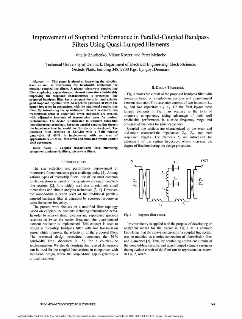
Fig. 1 shows the circuit of the proposed bandpass filter withtwo-zeros based on coupled-line sections and quasi-lumpedelement resonator. This resonator consists of two inductors L j,
L3, and two capacitors CJ, C4• On the final layout theselumped elements in Fig. 1 are realized in the form ofmicrostrip components, taking advantage of their wellpredictable performance in a wide frequency range andomission of via-holes for shunt capacitors.
Coupled line sections are characterized by the even- andodd-mode characteristic impedances ZOe, ZOo and theirrespective lengths. The elements Le are introduced foradjustment of the central frequency, which increases thedegree of freedom during the design procedure.
Fig. 1. Proposed filter circuit.
Inverter theory is applied with the purpose of developing ananalytical model for the circuit in Fig. 1. It is commonknowledge that the equivalent circuit of a coupled line sectioncan be modeled as a series connection of transmission linesand K-inverter [2]. Thus, by combining equivalent circuits ofthe coupled-line sections and quasi-lumped element resonatorthe equivalent circuit of the filter can be represented as shownin Fig. 2, where
547
Authorized licensed use limited to: Danmarks Tekniske Informationscenter. Downloaded on November 6, 2009 at 08:58 from IEEE Xplore. Restrictions apply.

821 =
p4LIL3C2C4 + p2(L1(C4+C2)+ L3C4)+ 1(4)
is the equivalent shunt conductance of the quasi-lumped
element resonator; j = H .
() () () ()
wherep = jm.This relation is based on the model representation shown in
Fig. 2 and relation (1). It can be easily seen that the resonatorintroduces two zeros in the transmission coefficient. Thelocations of the frequency transmission zeros can be found bysolving the quadratic equation in the numerator (4) and takinginto account frequency shifting due to Le•
Therefore, the overall frequency response of the filter hastwo transmission zeros as shown in Fig. 3. Obviously, thelocations of the transmission zeros for this filter may beadjusted by choosing suitable values for LJ,L3,C2,C4.
The characteristics of the filter can be derived from theABCD matrix for the complete circuit, which consists ofmatrices for the filter components:
EO~ -10
N(/J -20'0<U
-30"'C:J
:t:::CC) -40ro~
9 10 11 12 13 14
Frequency (GHz)
Fig. 3. Transmission characteristics for the traditional coupled-linefilter (broken line) and bandpass filter based on quasi-lumpedelement resonator (solid line).
(2)
Fig. 2. K-inverter type equivalent circuit of the filter.
where
are the ABCD parameters of the coupled line section with
characteristic impedance Z0 = JZOe •ZOo and electricallength () = ()e = ()o. Using this matrix representation, theelectrical parameters of the filter can be derived, and analysisof the circuit can be performed. The voltage transfer functionof the filter is determined as a product of the respectiveABCD matrices of the individual elements.
The nature of the transmission zeros creation may beillustrated by considering the relation for the transmissioncoefficient of the quasi-lumped element resonator labeled withY in Fig. 2:
JZoSinO][_o.cosO -.l
K
-JK][ ~~sOjSlnOo --Zo
(3)
JZo Sino]cosO
At the same time, due to selective properties of the quasilumped element resonator the spurious response at 210 issuppressed. For reference, the response of the traditionalcoupled-line filter is shown in Fig. 3. It can be seen that thesame coupled lines in a proposed configuration provide awider bandwidth. It is known that the wider bandwidthrequires a higher coupling level between lines in thetraditional coupled-line filter. The coupling level is related tothe gap dimension between lines. Therefore in practice, thefractional bandwidth of the traditional filter is limited bytechnological constraints. Considering the results presented inFig. 3, one can conclude that the proposed structure requireslower coupling level for the same frequency bandwidth incomparison to the conventional one.
III. FILTER IMPLEMENTATION AND RESULTS
The proposed filter shown in Fig. 1 is designed for afrequency band 4 -7 GHz and fabricated on a substrate withthe relative dielectric permittivity Gr = 3.38 and thicknessh = 0.8 mm. Values for the design parameters are presented inTable 1.
978-1-4244-1780-3/08/$25.00 © 2008 IEEE 548
Authorized licensed use limited to: Danmarks Tekniske Informationscenter. Downloaded on November 6, 2009 at 08:58 from IEEE Xplore. Restrictions apply.
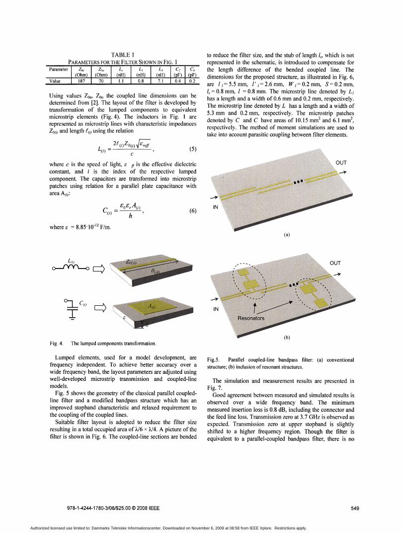
Using values ZOe, ZOo the coupled line dimensions can bedetennined from [2]. The layout of the filter is developed bytransfonnation of the lumped components to equivalentmicrostrip elements (Fig. 4). The inductors in Fig. 1 arerepresented as microstrip lines with characteristic impedancesZO(;) and length t(i) using the relation
2£ (i)ZO(i) J&ref!L(i) = c' (5)
where c is the speed of light, G ff is the effective dielectricconstant, and i is the index of the respective lumpedcomponent. The capacitors are transfonned into microstrippatches using relation for a parallel plate capacitance witharea Am:
Value
GoGrA(i)e(i) = h
where G = 8.85'10-12 F/m.
Fig. 4. The lumped components transformation.
(6)
to reduce the filter size, and the stub of length Is, which is notrepresented in the schematic, is introduced to compensate forthe length difference of the bended coupled line. Thedimensions for the proposed structure, as illustrated in Fig. 6,are 1[= 5.5 mm, I' [= 2.6 mm, W [= 0.2 mm, S= 0.2 mm,Is = 0.8 mm, I = 0.8 mm. The microstrip line denoted by LJ
has a length and a width of 0.6 mm and 0.2 mm, respectively.The microstrip line denoted by L has a length and a width of5.3 mm and 0.2 mm, respectively. The microstrip patchesdenoted by C and C have areas of 10.15 mm2 and 6.1 mm2
,
respectively. The method of moment simulations are used totake into account parasitic coupling between filter elements.
(a)
Lumped elements, used for a model development, arefrequency independent. To achieve better accuracy over awide frequency band, the layout parameters are adjusted usingwell-developed microstrip transmission and coupled-linemodels.
Fig. 5 shows the geometry of the classical parallel coupledline filter and a modified bandpass structure which has animproved stopband characteristic and relaxed requirement tothe coupling of the coupled lines.
Suitable filter layout is adopted to reduce the filter sizeresulting in a total occupied area of A/6 x A/4. A picture of thefilter is shown in Fig. 6. The coupled-line sections are bended
978-1-4244-1780-3/08/$25.00 © 2008 IEEE
Fig.5. Parallel coupled-line bandpass filter: (a) conventionalstructure~ (b) inclusion of resonant structures.
The simulation and measurement results are presented inFig. 7.
Good agreement between measured and simulated results isobserved over a wide frequency band. The minimummeasured insertion loss is 0.8 dB, including the connector andthe feed line loss. Transmission zero at 3.7 GHz is observed asexpected. Transmission zero at upper stopband is slightlyshifted to a higher frequency region. Though the filter isequivalent to a parallel-coupled bandpass filter, there is no
549
Authorized licensed use limited to: Danmarks Tekniske Informationscenter. Downloaded on November 6, 2009 at 08:58 from IEEE Xplore. Restrictions apply.
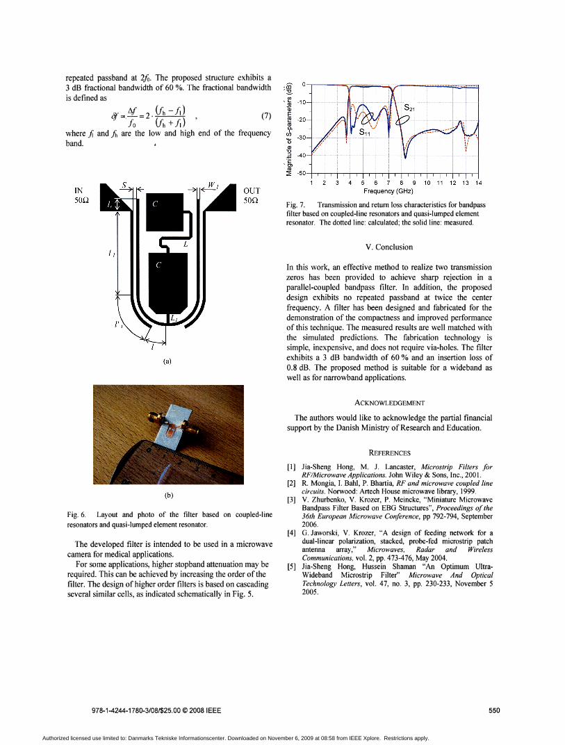
repeated passband at 2/0. The proposed structure exhibits a3 dB fractional bandwidth of 60 %. The fractional bandwidthis defined as
If =< N = 2. Vh - .Ii) (7)< fa Vh + fI)
where fi and fh are the low and high end of the frequencyband.
IN50n
(a)
OUT50n
.. 0) 0-r---'-~~o:iiiiiiii~~~~--r-...,..-.;~~~~~~
..~en'Q5 -1 0-+· .....•.... .,... .fI +......... ... +•..., +
Q)E~ -20--+···············:······#" ,' ·,,·v'··¥·'·· ····1111·'"'(,··,.,. ··+·· ; ,......., _ + •coc-oo~ -30-+···········~:. .. ········.··············~·····,····· + ........•......................~ 1/,.················;················;····· + I;f \j
oQ)
"C.a -40--f i························· ; + ,. ., +·v······+··················, .,..................................... I
'c'0)
ro~ -50 --+-.,--jr--r--+-r-+---.---+--T----+--r--+--r---t--1r-+--.---i--T---+-.--+-.-"i"'""-"T--I
2 3 4 5 6 7 8 9 10 11 12 13 14
Frequency (GHz)
Fig. 7. Transmission and return loss characteristics for bandpassfilter based on coupled-line resonators and quasi-lumped elementresonator. The dotted line: calculated~ the solid line: measured.
V. Conclusion
In this work, an effective method to realize two transmissionzeros has been provided to achieve sharp rejection in aparallel-coupled bandpass filter. In addition, the proposeddesign exhibits no repeated passband at twice the centerfrequency. A filter has been designed and fabricated for thedemonstration of the compactness and improved performanceof this technique. The measured results are well matched withthe simulated predictions. The fabrication technology issimple, inexpensive, and does not require via-holes. The filterexhibits a 3 dB bandwidth of 60 % and an insertion loss of0.8 dB. The proposed method is suitable for a wideband aswell as for narrowband applications.
(b)
Fig. 6. Layout and photo of the filter based on coupled-line
resonators and quasi-lumped element resonator.
The developed filter is intended to be used in a microwavecamera for medical applications.
For some applications, higher stopband attenuation may berequired. This can be achieved by increasing the order of thefilter. The design of higher order filters is based on cascadingseveral similar cells, as indicated schematically in Fig. 5.
978-1-4244-1780-3/08/$25.00 © 2008 IEEE
ACKNOWLEDGEMENT
The authors would like to acknowledge the partial financialsupport by the Danish Ministry ofResearch and Education.
REFERENCES
[1] Jia-Sheng Hong, M. 1. Lancaster, Microstrip Filters forRFIMicrowave Applications. John Wiley & Sons, Inc., 2001.
[2] R. Mongia, I. Bahl, P. Bhartia, RF and microwave coupled linecircuits. Norwood: Artech House microwave library, 1999.
[3] V. Zhurbenko, V. Krozer, P. Meincke, "Miniature MicrowaveBandpass Filter Based on EBG Structures", Proceedings of the36th European Microwave Conference, pp 792-794, September2006.
[4] G. Jaworski, V. Krozer, "A design of feeding network for adual-linear polarization, stacked, probe-fed microstrip patchantenna array," Microwaves, Radar and WirelessCommunications, vol. 2, pp. 473-476, May 2004.
[5] Jia-Sheng Hong, Hussein Shaman "An Optimum UltraWideband Microstrip Filter" Microwave And OpticalTechnology Letters, vol. 47, no. 3, pp. 230-233, November 52005.
550
Authorized licensed use limited to: Danmarks Tekniske Informationscenter. Downloaded on November 6, 2009 at 08:58 from IEEE Xplore. Restrictions apply.