improving system efficiency with a new intermediate-bus ... · pdf file4-1 topic 4 improving...
TRANSCRIPT

4-1
Topi
c 4
Improving System Efficiency with a New Intermediate-Bus Architecture
Rais Miftakhutdinov
AbstrAct
Ever growing demand for efficient and high quality tele- and data-communication power systems have driven the replacement of centralized power supplies with distributed architectures. Recently, a new Intermediate Bus design has gained popularity by providing lower cost, superior power quality, and higher efficiency while taking advantage of the newest advances in power components. This topic provides a brief overview of the historical evolution of high-reliability power systems, and then focuses on the benefits and design challenges of the Intermediate Bus Architecture (IBA) with an example illustrating the control requirements for a practical IBA converter design.
I. IntroductIon
Over the years, telecommunications and data-communications power-system architectures have transitioned through several basic topologies. The 1990s witnessed the transition from centralized power supplies to distributed-power architecture (DPA), with the most recent advance now called intermediate-bus architecture (IBA). Each advance of power-distribution systems has been driven by advances in components and circuit topologies and by a demand for wider input-voltage ranges, higher power levels, and better supply performance to support digital-processing systems. Other significant driving factors have been the general trends toward higher efficiency, smaller size, and lower cost of ownership for the whole electronic system.
The advantage of IBA depends heavily on an intermediate-bus converter (IBC) that generates an optimal intermediate-bus voltage and provides electrical isolation. Initially introduced in the early 2000s as a simplified version of a regulated isolated converter, the IBC has evolved as a new class of converter with very demanding requirements for high efficiency and power density. Depending on the input-voltage range and the electronic system’s requirements for voltage and power levels, the optimal IBC can be fully regulated, semiregulated, or unregulated, leaving many choices, trade-offs, and challenges to the power-system designer.
This topic starts with a general description of power-distribution systems for telecommuni-cations and data-communications equipment that requires high reliability and availability. It then introduces the role of the unregulated IBC as a key functional block of IBA-based power systems and provides a more in-depth review of the IBC’s major requirements and of the design of various IBC control methods. Finally, test results with a typical hardware example of a 48-V-input, 600-W-output IBC application are presented to demon strate the efficiency and improved performance of an IBC incorporating a new integrated controller with innovative features.
II. EvolutIon of PowEr-dIstrIbutIon systEms
Power-distribution systems for tele com muni-cations and data-communications equipment have undergone dramatic changes within the past two decades because of modern digital-processing equipment. Among the new priorities for a power system is that it be flexible enough to reliably handle interruption of input voltage and drastic load changes. Power systems are also required to be highly efficient, energy-saving, and “green” to reduce cost of ownership and meet environmental regulations while remaining compet i tive in the market. The brief history of telecommunications power-distribution systems that follows explains the reasons for power-system evolution.
4-2
Topi
c 4
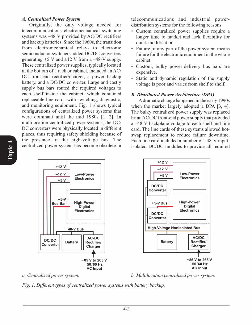
A. Centralized Power SystemOriginally, the only voltage needed for
telecommunications electromechanical switching systems was –48 V provided by AC/DC rectifiers and backup batteries. Since the 1960s, the transition from electromechanical relays to electronic semiconductor switchers added DC/DC converters generating +5 V and ±12 V from a –48-V supply. These centralized power supplies, typically located in the bottom of a rack or cabinet, included an AC/DC front-end rectifier/charger, a power backup battery, and a DC/DC converter. Large and costly supply bus bars routed the required voltages to each shelf inside the cabinet, which contained replaceable line cards with switching, diagnostic, and monitoring equipment. Fig. 1 shows typical configurations of centralized power systems that were dominant until the mid 1980s [1, 2]. In multilocation centralized power systems, the DC/DC converters were physically located in different places, thus requiring safety shielding because of the presence of the high-voltage bus. The centralized power system has become obsolete in
telecommunications and industrial power-distribution systems for the following reasons:
Custom centralized power supplies require a •longer time to market and lack flexibility for quick modification.Failure of any part of the power system means •failure for the electronic equipment in the whole cabinet.Custom, bulky power-delivery bus bars are •expensive.Static and dynamic regulation of the supply •voltage is poor and varies from shelf to shelf.
B. Distributed Power Architecture (DPA)A dramatic change happened in the early 1990s
when the market largely adopted a DPA [3, 4]. The bulky centralized power supply was replaced by an AC/DC front-end power supply that provided a –48-V backplane voltage to each shelf and line card. The line cards of these systems allowed hot-swap replacement to reduce failure downtime. Each line card included a number of –48-V input-isolated DC/DC modules to provide all required
Fig. 1. Different types of centralized power systems with battery backup.
a. Centralized power system. b. Multilocation centralized power system.
AC-DCRectifier/Charger
~85 V to 265 V50/60 HzAC Input
DC/DCConverter
+5-VBus Bar
+5 V
+12 V
–12 V
Battery
–48-V Bus
Low-PowerElectronics
High-PowerDigital
Electronics
AC/DCRectifier/Charger
Low-PowerElectronics
+5-VBus
+5 V
+12 V
–12 V
High-Voltage Nonisolated Bus
DC/DCConverter
DC/DCConverter
High-PowerDigital
Electronics
Battery
~85 V to 265 V50/60 HzAC Input

4-3
Topi
c 4
voltages to the line-card loads (Fig. 2). This change in the ideology about power distribution systems was driven by the following:
A trend towards digital functional blocks with •increased power, lower voltages, and specific power sequencingA broad market introduction of modular, high-•density, and reliable isolated DC/DC converters at a reasonable costA demand for a more flexible, shorter design •cycle for power-distribution systems that allowed quick changes and updatesA need for systems with high reliability and •availability that supported hot swapping and had lower maintenance costs
C. Hybrid Power SystemDPA-based systems addressed new power
requirements, but the system cost remained relatively high. When the required number of supply voltages per line card exceeded the initial four to five, the excessive number of isolated DC/DC converters was questioned. In Reference [5], Narveson suggested using only one isolated DC/DC converter and deriving the remaining outputs from nonisolated point-of-load (POL) regulators.
This architecture, commonly called a hybrid power system (Fig. 3), was the first step towards the IBA. The hybrid power system reduces power-distribution costs and allows placing POLs right next to the related load, thus reducing the impact of supply-plane parasitics and improving high-di/dt transient response.
The hybrid power system is the preferred solution when one of the output voltages requires relatively high power. In this case, a single regulated, isolated converter improves the efficiency of the whole system when the converter’s
Fig. 2. Example of distributed-power architecture.
Consideration Area
AC/DC
PowerSupply 1
Power Supply 2(Redundant)
Slots 1–9(Right to Left)
SupervisorEngine
RedundantSupervisorEngine
SwitchingModules
ESD Ground StrapConnection
FanAssembly
~85 to 265 V
Module #1(Line Card)
Module #N(Line Card)
–48-V Backplane
Fig. 3. Hybrid power system.
Regulated, IsolatedDC/DC Converter
DC SystemBus
Options:
24 V nom,–48 V nom,400 V nom
POL
POL
POL
POL
POL
12 V(Low Power)
3.3 V
2.5 V
1.8 V
1.2 V
5 V(High Power)

4-4
Topi
c 4
output voltage is 3.3 V or higher. With the 3.3-V bus voltage, the hybrid system’s overall power output may be limited to about 200 W. This limit is suggested because high currents circulating through the bus-voltage power and ground planes can cause significant losses and EMI issues as the system power increases.
D. Intermediate-Bus Architecture (IBA)Driven by demands from the digital- and
analog-IC industry for low-cost POLs and for an increasing number of low-level supply voltages in the 0.5- to 3.3-V range, the early 2000s market adopted the IBA [6-8]. In many applications, the IBA-based power system includes a front-end AC/DC power supply with a typical output of 24 V or –48 V. In some data-communications and medical equipment, the input DC voltage can be from a 400-V power-factor-corrector block [9]. This voltage is supplied to an IBC that provides isolation and conversion to the lower-level intermediate-bus voltage, typically 5 to 14 V. This intermediate-bus voltage is supplied to nonisolated, POL regulators that provide high-quality voltages for a variety of digital and analog electronic blocks (Fig. 4).
Advantages of an IBA SystemSystem cost is reduced because only one isolated •converter is needed and because low-cost, standardized nonisolated POL regulators are available in the market.IBC designs can be simple because there are no •strict regulation requirements for the intermediate-bus voltage.Quality of supply voltages is increased because •nonisolated POLs are located next to the electronic functional blocks.
System has high flexibility for modifications •and updates.Overall system reliability is higher.•Housekeeping, power sequencing, diagnostics, •and optimized power-saving modes are easier to implement because all major control signals are on the secondary side.
Potential Challenges for an IBA SystemThe intermediate-bus converter must have the •highest efficiency and power density to provide a competitive edge for IBA versus DPA.The overall line-card power can be limited •because of high currents circulating through ground- and bus-voltage planes.Parallel operation of highly efficient, unregulated •bus converters can be difficult.Specialized IBC controller ICs are needed to •address specific IBC requirements.
E. Comparison and Trade-Offs of IBA versus DPA
IBA is a continuation of DPA at the line-card level. An optimal choice between IBA and standard DPA for each specific case depends on many factors, including the number of required power supplies, the required voltage and power levels, the system-bus input-voltage range, and the specified static and dynamic regulation. It is obvious that cost and efficiency are the most significant trade-offs. Table 1 shows the pros and cons between IBA- and DPA-based systems in very general terms. A detailed analytical comparison is needed to make the right design decision. Examples of such analysis can be found in Reference [10].
Fig. 4. Example of IBA.
Intermediate-BusConverter
(DC/DC Transformer)
DC SystemBus
Options:
24 V nom,–48 V nom,400 V nom
POL
POL
POL
POL
POL
POL
12 V
3.3 V
2.5 V
1.8 V
1.2 V
5 V
Intermediate-Bus Voltage:
5 V nom,8 V nom,12 V nom
4-5
Topi
c 4
III. KEy ElEmEnts of Ibc dEsIgn
IBA includes an additional DC/DC conversion stage provided by an IBC to supply the intermediate-bus voltage (Fig. 4). It is important for the IBC to be highly efficient with high component density at the lowest possible cost. While the first bus converters on the market were slightly modified versions of fully regulated DC/DC modules, the IBC’s strict design requirements have made it a stand-alone, specialized product in module manufacturers’ portfolios.
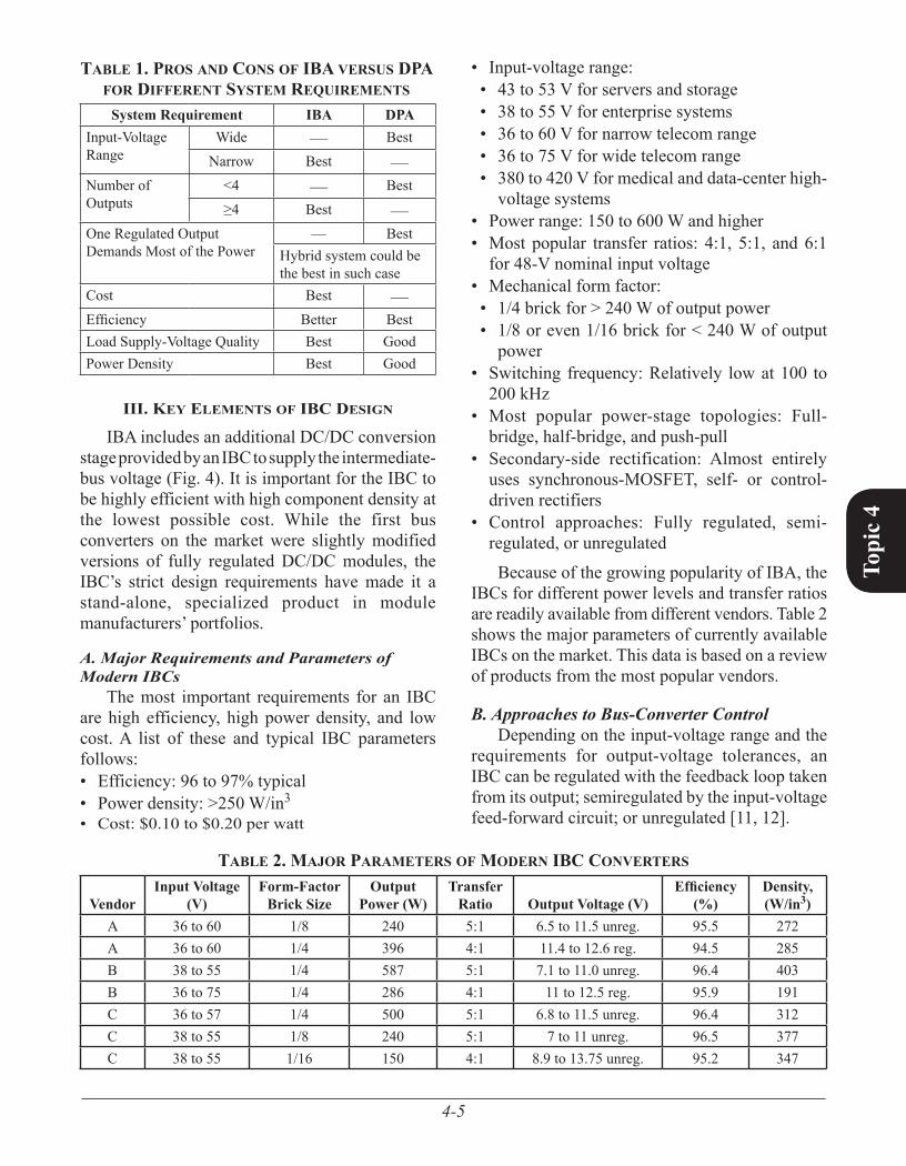
A. Major Requirements and Parameters of Modern IBCs
The most important requirements for an IBC are high efficiency, high power density, and low cost. A list of these and typical IBC parameters follows:
Efficiency: 96 to 97% typical•Power density: >250 W/in• 3
Cost: $0.10 to $0.20 per watt•
Input-voltage range: •43 to 53 V for servers and storage•38 to 55 V for enterprise systems•36 to 60 V for narrow telecom range •36 to 75 V for wide telecom range•380 to 420 V for medical and data-center high-•voltage systems
Power range: 150 to 600 W and higher •Most popular transfer ratios: 4:1, 5:1, and 6:1 •for 48-V nominal input voltageMechanical form factor: •1/4 brick for > 240 W of output power•1/8 or even 1/16 brick for < 240 W of output •power
Switching frequency: Relatively low at 100 to •200 kHzMost popular power-stage topologies: Full-•bridge, half-bridge, and push-pullSecondary-side rectification: Almost entirely •uses synchronous-MOSFET, self- or control-driven rectifiersControl approaches: Fully regulated, semi-•regulated, or unregulated
Because of the growing popularity of IBA, the IBCs for different power levels and transfer ratios are readily available from different vendors. Table 2 shows the major parameters of currently available IBCs on the market. This data is based on a review of products from the most popular vendors.
B. Approaches to Bus-Converter ControlDepending on the input-voltage range and the
requirements for output-voltage tolerances, an IBC can be regulated with the feedback loop taken from its output; semiregulated by the input-voltage feed-forward circuit; or unregulated [11, 12].
System Requirement IBA DPAInput-Voltage Range
Wide — BestNarrow Best —
Number of Outputs
<4 — Best≥4 Best —
One Regulated Output Demands Most of the Power
— BestHybrid system could be the best in such case
Cost Best —Efficiency Better BestLoad Supply-Voltage Quality Best GoodPower Density Best Good
tAblE 1. Pros And cons of IbA vErsus dPA for dIffErEnt systEm rEquIrEmEnts
VendorInput Voltage
(V)Form-Factor
Brick SizeOutput
Power (W)Transfer
Ratio Output Voltage (V)Efficiency
(%)Density, (W/in3)
A 36 to 60 1/8 240 5:1 6.5 to 11.5 unreg. 95.5 272A 36 to 60 1/4 396 4:1 11.4 to 12.6 reg. 94.5 285B 38 to 55 1/4 587 5:1 7.1 to 11.0 unreg. 96.4 403B 36 to 75 1/4 286 4:1 11 to 12.5 reg. 95.9 191C 36 to 57 1/4 500 5:1 6.8 to 11.5 unreg. 96.4 312C 38 to 55 1/8 240 5:1 7 to 11 unreg. 96.5 377C 38 to 55 1/16 150 4:1 8.9 to 13.75 unreg. 95.2 347
tAblE 2. mAjor PArAmEtErs of modErn Ibc convErtErs

4-6
Topi
c 4
The IBC with a closed feedback loop requires an additional isolation barrier for feedback-signal transfer. It is more expensive and less efficient than a semiregulated or unregulated IBC because it operates in a wide duty-cycle range. However, full regulation is justified for the hybrid power system where the IBC’s output is the supply voltage for the most power-consuming load. If power sequencing is needed, an additional switch can be added between the IBC’s output and the load [12].
The IBC that is semiregulated by the input-voltage feed-forward circuit is usually a lower-cost solution than the fully regulated converter, but it also has lower density and efficiency than the unregulated converter because it is designed to operate over a wide duty-cycle range, even at steady state. The semiregulated IBC may also be used in a system with a relatively wide input-voltage range.
The unregulated IBC provides the solution with the highest efficiency and power density and the lowest cost because it operates at almost 100% duty cycle at steady state. There is no additional
communication through the isolation barrier except for the energy transfer through the power transformer. The size of the transformer and its output and input filters is small because the converter operates at maximum duty cycle. However, overstresses that occur during transient conditions like start-up, current limiting, and shutdown need to be addressed during the design.
C. Major IBC TopologiesIBCs are usually highly efficient because they
can employ forward-type full-bridge, half-bridge, and push-pull topologies and the synchronous-MOSFET rectification technique. Fig. 5 shows three such IBCs in their very simplified forms. Using a self-driven, synchronous-MOSFET rectifier is a very popular choice for unregulated converters, but practical solutions may require additional control windings and snubber circuits for improved efficiency and reliability. Despite the popularity of using such rectifiers in unregulated bus converters, high-power applications for fully regulated and semiregulated converters with control-driven MOSFET rectifiers can be used as
Fig. 5. Popular power-stage topologies for IBC.
a. Full-bridge IBC. B. Half-bridge IBC. C. Push-pull IBC.
Vout +–
Vin
+
–
Q1
Q11 Q22
Q3 Q4
Lout
Rout
Cout
Q2 Q1
Q11 C1
Q3 Q4
C2
Vout +–
Vin
+
–
Lout
Rout
Cout
Q1
Q3 Q4
Q2
Vout +–
Vin
+
–
Lout
Rout
Cout

4-7
Topi
c 4
well. Two advantages of using control-driven rectifiers are a simplified power transformer and a gate-drive voltage that is independent from input-voltage and load-current variations. A detailed review, classification, and comparison of synchronous-rectification techniques can be found in Reference [13].
The double-ended topologies shown in Fig. 5 are preferred for IBC applications because they can operate at almost 100% duty cycle, which can significantly reduce the size of the output inductor. Currently available IBCs usually operate at about 100 kHz. They can operate with a 48-V (nominal) input-voltage range in the hard-switching mode, or with a 400-V (nominal) input-voltage range in the zero-voltage-switching transition mode. The full-bridge topology is preferred for a 250-W or higher output power. The half-bridge topology provides a low-cost solution for the output-power range below 250 W. The bridge-based topologies have primary MOSFETs with a drain-to-source voltage rating equal to the input voltage, with some reliability margin. These topologies are a better choice for input voltages higher than 24 V. For a 24-V or lower input, the simplicity of push-pull topology is attractive because driving primary MOSFETs is easier. However, the center-tapped primary winding is a drawback for the planar transformer.
Table 3 provides a general comparison of IBC topologies. However, to select the right topology during practical design, detailed calculations and a review of power-system specifications are needed for each specific case.
D. Using a Resonant Converter as an Unregulated IBC
Recent published reports, among them Reference [14], have suggested that a high-frequency, resonant-converter topology can be used for a high-performance, unregulated IBC. This topology has been successfully used for bus converters operating at up to 800 kHz at 95.5% efficiency with a 48-V input and a 12-V, 500-W output but has not yet become mainstream in the industry.
Iv. chAllEngEs of dEsIgnIng unrEgulAtEd Ibcs
The design of unregulated IBCs with self-driven MOSFET rectification has its own challenges with numerous trade-offs. The design goal is to achieve the highest efficiency and power density at the lowest cost. The challenges include the following:
High ripple current during transitional states•Start-up problems•Optimal synchronous rectification•Reverse energy flow and self-oscillation•Parallel-operation issues•Flux balancing of power transformer•
The following discussion (Sections A through F) addresses each of these challenges.
A. Operation at Transitional StatesAt steady state, an unregulated converter
operates at almost 100% duty cycle with very low output ripple current and low input-inductor ripple current. However, during softstart or cycle-by-cycle current limiting, the duty cycle varies from 0% to 100%, which can cause a significant ripple increase at the middle of this range. This ripple can overstress the power stage and limit the start-up capabilities of the IBC, especially when there is a large output capacitance. The output inductor’s
Topology Full-Bridge Half-Bridge Push-PullPrimary
MOSFETSVds = Vin Vds = Vin Vds > 2Vin
Transformer Good utilization
Problem with 5:1
transfer ratio
Poor utilization
RectifierMOSFETs
Primary-winding clamping to zero is possible
No primary-winding clamping
ability
No primary-winding clamping
ability
Output Inductor
The Same
Cycle-by-Cycle Current Limit
Only a problem if a DC blocking capacitor is
used
Inherent issue
Not a problem
tAblE 3. comPArIson of PoPulAr Ibc toPologIEs

4-8
Topi
c 4
peak-to-peak ripple current, ΔIL, can be plotted with Equation (1) for the whole duty-cycle range:
∆I
V D D
N L fLin
tr out sw= −× ×
× × ×( )
,1
2 (1)
where fsw = 1/Tsw is the switching frequency, D = Ton/(0.5 × Tsw) is the duty cycle after rectification, Ntr = Wpr/Wsec is the transformer’s transfer ratio, Wpr is the primary winding turns, Wsec is the secondary winding turns, Lout is the inductor’s inductance, and Vin is the voltage to the transformer’s primary winding.
Equation (1) gives the corrected inductor ripple current as
∆I
V
N L kLin
tr out=
2× × ×.
(3)
The result of the correction is that the switching frequency changes as the duty cycle changes to maintain the inductor’s ripple current at a constant value. This idea has been implemented in the Texas Instruments (TI) UCC28230/1 controller [15]. A measured plot of the switching-frequency change versus the duty cycle is shown in Fig. 7. In this case, the nominal switching frequency is set at about 100 kHz. The frequency is maintained constant during steady-state operation when the duty cycle is above 90% or less than 10%. During start-up or cycle-by-cycle current limiting, the duty cycle varies significantly such that the inductor’s ripple current reaches a maximum value at 50% duty cycle. The frequency-control circuit maintains the maximum frequency at about 420 kHz when the duty cycle is between 30% and 70%. The higher frequency significantly reduces ripple current and allows the output inductor to be approximately 25% of the value needed without the frequency-control circuit. When the frequency-control circuit is used, inductor selection is based on a maximum frequency of 420 kHz at 50% duty cycle instead of on 100 kHz as it would be without frequency control.
Fig. 6. Output inductor’s ripple current versus duty cycle for a 48-V input, 5:1 transfer ratio, and 0.1-µH output inductor.
0 10 20 30 40 50 60 70 80 90 1000
20
40
60
80
100
120
140
Duty Cycle, D (%)
Indu
ctor
Rip
ple
Cur
rent
,I
( A)
L
pk-p
k
100 kHz
200 kHz
500 kHz
Note that duty-cycle calculations assume a D value between 0 and 1. The following discussion refers to duty cycle in percent, which is D × 100.
The plots in Fig. 6 show that the output inductor’s ripple current is very low in the vicinity of D = 0 and 100% but can reach 120 A at D = 50%. Thus, the size and cost of power-stage components, especially of the output inductor, become significantly higher when this increased transitional peak ripple current has been taken into account.
One way to avoid the issue of high ripple current is to use a special frequency-control circuit that limits the output inductor’s ripple current during duty-cycle transitions between 0% and 100%. The desired change in switching frequency over the duty-cycle range is
f k D Dsw = −× × ( ),1 (2)where k is a constant based on circuit implementation. Substituting Equation (2) into
0 10 20 30 40 50 60 70 80 90 1000
100
200
300
400
500
Duty Cycle, D (%)
Switc
hing
Freq
uenc
y,f
(kHz)
sw
Fig. 7. Measured switching frequency versus duty cycle with frequency-control circuit.

4-9
Topi
c 4
V
V IR
ND
NI Rout
in outpr
tr
trout=
−
−× ×
× sec ,
(5)
where Rpr is the equivalent series resistance of the power-stage primary side, and Rsec is the equivalent series resistance of the secondary side.
The plots in Fig. 8a show output voltage versus average load current at steady state and during start-up operation with cycle-by-cycle current limiting. These plots were determined by
B. Startup ProblemsThe ripple increase described in the
previous section also impacts IBC start-up. The inductor’s ripple-current increase during start-up may activate the IBC’s overcurrent-protection circuit, possibly causing the converter not to start at all. Increasing the current-sensing threshold level and adding more filtering are not recommended for correcting a start-up problem. If a real overcurrent or output short circuit occurs, these methods of correction will probably overstress the converter. To meet reliability and current-stress margin requirements for the power-stage components, a much larger output inductor must be selected, or the switching frequency must be increased to reduce the ripple (Fig. 6).
To further illustrate the start-up issue, the plots in Fig. 8 of output voltage versus average load current are presented based on the following analysis. During the cycle-by-cycle current limit, the inductor’s average output current, Iout, can be described by Equations (4) and (5):
I IN V D
L f
V D D
N L f
out otr in
m sw
in
tr out sw
= −
− −
(lim)
( ),
× ××
× ×× ×
4
1
4
(4)
where Io(lim) is the output current limit and Lm is the primary magnetizing inductance of the power transformer. Then for any Iout range, the output voltage, Vout, can be determined as follows:
Fig. 8. IBC start-up performance with 75-A cycle-by-cycle current limit and 100-kHz nominal switching frequency.
a. Without frequency-control circuit (fsw(max) = 100 kHz).
b. With frequency-control circuit (fsw(max) = 420 kHz).
0 10 20 30 40 50 60 70 800
2
4
6
8
10
12
I (A)out
V(V)
out
V at Steady Stateout
V During Start-Up(Limited by ripple current)out
Constant R = 0.45
ConstantP = 60 W Constant I = 11.5 A
0 10 20 30 40 50 60 70 800
2
4
6
8
10
12
I (A)out
V(V)
out
V at Steady Stateout
VDuringStart-up
outConstant R = 0.125
Constant P = 300 W Constant I = 59.5 A
substituting Equation (4) into Equation (5) with the following conditions: Vin = 48 V, fsw = 100 kHz, Ntr = 5, Lout=0.1μH,Lm=75μH,Io(lim) = 75 A, Rpr=25mΩ,andRsec=4mΩ.
Also included in Fig. 8a are the start-up load curveswithaconstantloadresistanceof0.45Ω,aconstant current load of 11.5 A, and a constant power load of 60 W. The constant-resistance and constant-current curves are touching the start-up Vout versus Iout curve without crossing it. With the

4-10
Topi
c 4
constant-power mode replicating POL-regulator behavior, it is assumed that the POL regulator starts operating and draws current only after Vout exceeds the undervoltage lockout (UVLO) threshold set at 5 V. Until then, the POL regulator does not draw any current. Thus, the load curves indicate the maximum start-up load current of a converter designed for 60-A nominal output with a current limit set at 75 A. Obviously, the fold-back behavior of Vout versus Iout limits the start-up capability of this unregulated IBC. The load curves cross the steady-state Vout (upper) plot at 21 A for the constant-resistance mode, at 11.5 A for the constant-current mode, and at 5 A for the constant-power mode. The start-up performance of the converter is reduced dramatically because of the inductor’s large ripple current at 50% duty cycle. Without the frequency-control circuit suggested earlier, the only way to override this limitation is to either increase the output inductance or increase the nominal switching frequency. Either way, power losses and converter cost increase.
Fig. 8b illustrates the advantage of a start-up frequency-control circuit. The conditions are the same as for Fig. 8a except that the converter operates at 420 kHz for most of the start-up time and at 100 kHz when it reaches the steady-state condition.Withthesame0.1-μHoutputinductor,the start-up capability is significantly improved over that shown in Fig. 8a where fsw(max) = 100 kHz. The load curves cross the steady-state Vout curve at 75 A for constant-resistance mode, at 59.5 A for constant-current mode, and at 32 A for constant-power mode.
This start-up analysis is based on the assump-tion that the IBC’s output capacitor is not very large. Obviously, if the allowable start-up time is short and the output capacitor is large, an additional current to charge the high capacitance must be taken into account. The frequency-control circuit
Fig. 9. IBC’s required charge current for different output capacitances at selected soft-start time.
0.1 1 100.01
0.1
1
10
100
1000
Soft-Start Time (ms)
Cha
rge
Cur
rent
(A)
C = 100 µFOUT
C = 1000 µFOUT
C = 10000 µFOUT
increases the average charge current available for start-up even with a large output capacitor. The average charge current, Ich, for the output capacitor, Cout, that satisfies the selected soft-start time, tss, can be determined by Equation (6):
I C
V
t Nch outin
ss tr= ×
× (6)
Fig. 9 shows the IBC’s average output current required to charge different output capacitances for the selected soft-start time. These curves do not account for the extra current drawn by the load. The effects of different output capacitances can be estimated with and without a frequency-control circuit by comparing the plots in Figs. 8 and 9.
With the frequency-control circuit, a charge current of at least 59.5-A is available per Fig. 8b. A 10-A portion of this current can be used to charge the 10000-μF output capacitor within 10 ms per Fig. 9. The remaining 49.5-A current is available to the load.
Without the frequency-control circuit, the available current per Fig. 8a is only 11.5 A. This currentisbarelysufficienttochargethe10000-μFoutput capacitor within 10 ms. If the load draws more than 1.5 A in addition to the capacitor’s charge current, the converter will not start because the overcurrent-protection circuit will be activated due to the large ripple current.

4-11
Topi
c 4
C. Optimal Synchronous Rectification Technique
For IBCs with a 12-V or lower output voltage, the synchronous-rectification technique is mandatory to achieve the required efficiency. Compared to Schottky diodes, low-RDS(on) rectifier MOSFETs can increase IBC efficiency by more than 5%. There are many publications and patented solutions for how to drive the rectifier MOSFETs. Most designs can be divided into self-driven, control-driven, and diode-emulator categories. Classification of synchronous rectification and additional details can be found in Reference [13]. For the unregulated IBC, a self-driven rectification approach that uses a secondary-side transformer winding (Fig. 5) or an additional control winding is quite popular because of its simplicity. The proper timing in either self-driven or control-driven synchronous rectifiers is critical to reduce power losses. To avoid overshoot, it is important that the conducting rectifier MOSFET on the secondary side turn off before the primary-side
MOSFET is turned on. This is achieved by proper OFF-time switching control of primary-side MOSFETs for half-bridge (Fig. 5b) and push-pull (Fig. 5c) topologies. For the full-bridge topology (Fig. 5a), the OFF time is specified to be the time between primary current switching of MOSFETs on one diagonal to MOSFETs on the other diagonal. The optimal OFF time, Toff(opt), depends on power-stage parameters and the load current. With light loads, the optimal OFF time is longer. This relationship is illustrated in the drain-source and gate-source switching waveforms of the synchronous-rectifier MOSFETs shown in Fig. 10a for no load and in Fig. 10b for nominal current conditions.
Optimal switching of rectifier MOSFETS over a wide load-current range is possible when the OFF time is allowed to increase to some degree at light loads but is kept as short as possible with nominal loads. A special OFF-time control circuit can be designed to allow the desired output-current threshold to be set such that the OFF time, Toff,
Fig. 10. Switching waveforms of secondary-side rectifier MOSFETs.
a. No load, 50 ns/div. b. 44-A load current, 25 ns/div.
Q3, V (5 V/div)gs
V = 48 V, I = 0 A, f = 100 kHzin L SW
Q4, V (10 V/div)ds
Time (50 ns/div)
Q3, V (10 V/div)ds
Q4, V (5 V/div)gsQ3, V (5 V/div)gs
V = 48 V, I = 44 A, f = 100 kHzin L SW
Q4, V (10 V/div)ds
Time (25 ns/div)
Q3, V (10 V/div)ds
Q4, V (5 V/div)gs

4-12
Topi
c 4
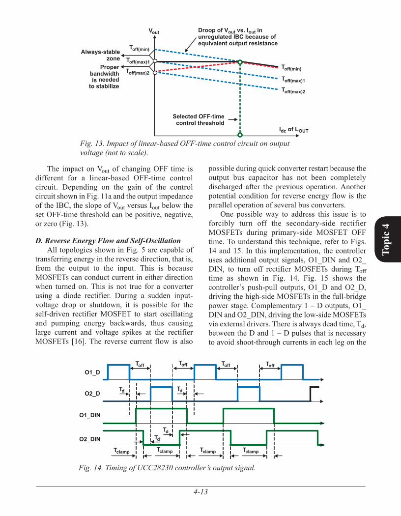
starts increasing and reaches its maximum at no-load condition (Fig.11). This increase can be implemented in a linear manner as shown in Fig. 11a, or as a step function with hysteresis as shown in Fig. 11b. The method can vary depending on the specific design and application. TI’s specialized UCC28230/1 bus-converter controller implements a comparator-based approach as shown in Fig. 11b. This controller has dedicated pins (OS and OST) to allow programming of the nominal OFF time, Toff, and the output-current threshold so the OFF time steps up to the new Toff(max) value at the desired current level. The gray area designated “Tclamp” in Fig. 11 represents the time when both rectifier MOSFETs are turned off. The purpose of Tclamp is to prevent reverse energy flow, which is described in detail in Section IV. D.
Since the unregulated IBC does not have direct access so it can sense the load current, a transformer current tap or primary-side resistor is usually used to monitor output current indirectly. Primary-side current sensing includes not only the reflected load current but also the magnetizing current. However, in most applications, the magnetizing current is only a small percentage of overall current and can be ignored.
The impact of increasing OFF time in relation to output voltage during light-load conditions is shown by Equation (7):
VV
N
t T
tI Rout
in
tr
s off
sout out= × − − ×
(7)
For the comparator-based approach shown in Fig. 11b, the output voltage (Vout) can jump a few hundred millivolts (with hysteresis) as shown in Fig. 12. This jump is not desirable if IBC’s operate in parallel using droop-current sharing. For such applications, the OFF-time control circuit can be disabled to allow constant-slope output voltage.
OFF-time Control Threshold(Set by resistor divider R1/R2 frompin VREF to pin OST and to GND)
00
Iout
T = 2.5 Toff(opt) d at heavy load(set by resistor R3 from
pin OS to GND)
T at no load = 5off T for 20%off(opt)OFF-time control threshold
Toff
Tclamp
Td
Td
Tclamp
Ensuresno cross
conduction atlight load
Providesminimum diodeconduction overwide range ofload conditions
OFF-time Control Threshold(Set by resistor divider R1/R2 frompin VREF to pin OST and to GND)
00
Iout
T = 2.5 Toff(opt) d at heavy load(set by resistor R3 from
pin OS to GND)
T at no load = 5off(max) T for 20%off(opt)OFF-time control threshold
Toff
Td
Td
Td
Ensuresno cross
conduction atlight load
Providesminimum diodeconduction overwide range ofload conditions
Hysteresis = I R1 R2/(R1 + R2)HYST
Tclamp
Tclamp
a. Linear OFF-time control.
b. Step-change OFF-time control.
Fig. 11. Setting Toff, Td, and Tclamp versus load current with OFF-time control circuit.
Hysteresis to avoidinstability fromLC filter ringing
I of Ldc out
Vout
Toff(min)Toff(max)1Toff(max)2
Toff(min)
Toff(max)1Toff(max)2
Selected OFF-timecontrol threshold
Droop of V vs. I inunregulated IBC because ofequivalent output resistance
out out
Fig. 12. Impact of comparator-based OFF-time control circuit on output voltage (not to scale).
4-13
Topi
c 4
The impact on Vout of changing OFF time is different for a linear-based OFF-time control circuit. Depending on the gain of the control circuit shown in Fig. 11a and the output impedance of the IBC, the slope of Vout versus Iout below the set OFF-time threshold can be positive, negative, or zero (Fig. 13).
D. Reverse Energy Flow and Self-OscillationAll topologies shown in Fig. 5 are capable of
transferring energy in the reverse direction, that is, from the output to the input. This is because MOSFETs can conduct current in either direction when turned on. This is not true for a converter using a diode rectifier. During a sudden input-voltage drop or shutdown, it is possible for the self-driven rectifier MOSFET to start oscillating and pumping energy backwards, thus causing large current and voltage spikes at the rectifier MOSFETs [16]. The reverse current flow is also
possible during quick converter restart because the output bus capacitor has not been completely discharged after the previous operation. Another potential condition for reverse energy flow is the parallel operation of several bus converters.
One possible way to address this issue is to forcibly turn off the secondary-side rectifier MOSFETs during primary-side MOSFET OFF time. To understand this technique, refer to Figs. 14 and 15. In this implementation, the controller uses additional output signals, O1_DIN and O2_DIN, to turn off rectifier MOSFETs during Toff time as shown in Fig. 14. Fig. 15 shows the controller’s push-pull outputs, O1_D and O2_D, driving the high-side MOSFETs in the full-bridge power stage. Complementary 1 – D outputs, O1_DIN and O2_DIN, driving the low-side MOSFETs via external drivers. There is always dead time, Td, between the D and 1 – D pulses that is necessary to avoid shoot-through currents in each leg on the
Vout
Always-stablezone
Properbandwidthis neededto stabilize
Selected OFF-timecontrol threshold
Droop of V vs. I inout outunregulated IBC because ofequivalent output resistance
I of Ldc OUT
Toff(min)Toff(max)1Toff(max)2
Toff(min)
Toff(max)1Toff(max)2
Fig. 13. Impact of linear-based OFF-time control circuit on output voltage (not to scale).
Td Td
TdTd
Toff Toff Toff Toff
Tclamp Tclamp Tclamp Tclamp
O1_D
O1_DIN
O2_DIN
O2_D
Fig. 14. Timing of UCC28230 controller’s output signal.

4-14
Topi
c 4
primary side. If the duty cycle is less than maximum, there is the overlapping time, Tclamp, when the primary winding is shorted by the lower MOSFETs because they are both in the ON state (Figs. 14 and 15). This specific timing algorithm has been implemented in UCC28230/1 controllers.
As mentioned earlier, this timing technique addresses the problem of reverse current flow during output prebias start-up, shutdown, input-voltage drop, or parallel operation. For the half-bridge (Fig. 5b) or push-pull (Fig. 5c) IBC topologies, the primary winding of the power transformer cannot be shorted by the primary power MOSFETs. To turn off the secondary-side rectifier MOSFETs during the Tclamp interval, an external pulse transformer can be used as shown in Fig. 16. In this case, the synchronous-rectifier scheme uses the control-driven technique for the unregulated IBC.
E. Parallel-Operation IssuesParallel operation of IBCs is desirable in cases
when the physical height is limited or when there may be a future need to easily upgrade to higher power levels. Paralleling can also be used for N+1 redundancy, but in this case, diodes in series with the outputs are needed to isolate a failed converter from the rest of the system. It is impossible to use any kind of active current-sharing technique with parallel unregulated converters. The only option here is to use a droop-current-sharing mechanism that depends on the output impedance of the converters sharing the current. Obviously, an accurate droop-current-sharing approach becomes more difficult as new IBC designs become more efficient. Additional problems related to sharing steady-state current can occur if all parallel IBCs do not start simultaneously. These problems include power circulation and tripping the overcurrent-protection circuit. Maintaining the secondary-side rectifier MOSFETs in the OFF
+
_
CT
+
_
UCC27200Vbias
Vbias
Vbias
V36 to 60 V
in
V7 to 12 V400 W
out
UCC27200
UCC28230/1
BiasPowerSupply
OptionalMicrocontroller
VREF
VDDVDD
VDD
VDD
RTCLK
EN
CS
SS
Vin
OS
UVLOComp.
R1
R2
1
12
10
8
11
9
7
5
2
6
4
3
OST
R3 Short-CircuitShutdown
LogicBlockCycle-by-Cycle
Current Limit
Oscillatorand Start-UpFrequencyControl
ReferenceGenerator
O1_DIN
O1_D
O2_DIN
O2_D
GND
5-V/3.3-VLDO
OFF-TimeControlCircuit
Soft Start andHiccup Current-Limit Circuit
ThermalShutdown
Interfacewith
System
V = 5 Vor 3.3 VCC
Fig. 15. Simplified diagram of typical full-bridge unregulated IBC.

4-15
Topi
c 4
state during the 1 – D cycle previously described is one way to prevent reverse current flow during parallel operation of unregulated IBCs.
F. Flux Balancing of Power Transformer For optimal operation with reduced switching
losses, unregulated IBCs use a relatively low 100- to 200-kHz switching frequency. The power transformer in the topologies shown in Fig. 5 are expected to operate with a symmetrical hysteresis (B-H) loop with no flux unbalancing for smaller size. One option to avoid flux unbalancing is to use a gapped transformer. However, this approach requires more transformer magnetizing current. Another option is to use a DC-blocking capacitor in series with the primary winding as shown in Fig. 5a for the full-bridge converter. For the half-bridge topology, this capacitor is already present as a necessary part of the power stage (Fig. 5b). The potential issue with the DC-blocking capacitor is that during cycle-by-cycle current limiting,
significant variations in pulse amplitudes may be applied to the primary winding. This pulse variation occurs because significant DC voltage can build up across the blocking capacitor that can interfere with the transformer’s volt-second balance each half switching cycle. Unequal amplitude pulses to the transformer windings cause overvoltage stresses in the secondary-side rectifier MOSFETs. In many cases, careful layout and symmetrical matched-output pulses from the controller and drivers can eliminate the need for a DC-blocking capacitor in the full-bridge converter. The simplest way to avoid unbalancing in a push-pull converter is to use cycle-by-cycle current limiting or a gapped transformer, because the DC-blocking capacitor cannot be used with this topology.
+
_
CT
+
_
Interfacewith
System
UCC27200Vbias
Vbias
V = 5 Vor 3.3 VCC
Vbias
V36 to 60 V
in
V7 to 12 V200 W
out
UCC28230/1
UCC27324
BiasPowerSupply
OptionalMicrocontroller
VREF
VDDVDD
VDD
VDD
RTCLK
EN
CS
SS
Vin
OS
UVLOComp.
R1
R2
1
12
10
8
11
9
7
5
2
6
4
3
OST
R3 Short-CircuitShutdown
LogicBlockCycle-by-Cycle
Current Limit
Oscillatorand Start-UpFrequencyControl
ReferenceGenerator
O1_DIN
O1_D
O2_DIN
O2_D
GND
5-V/3.3-VLDO
OFF-TimeControlCircuit
Soft Start andHiccup Current-Limit Circuit
ThermalShutdown
Fig. 16. Typical half-bridge unregulated IBC with control-driven synchronous rectifier.
4-16
Topi
c 4
v. ExPErImEntAl rEsults
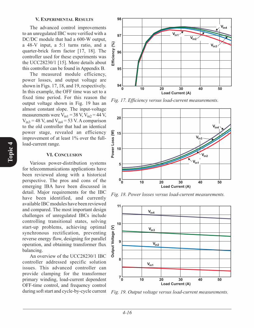
The advanced control improvements to an unregulated IBC were verified with a DC/DC module that had a 600-W output, a 48-V input, a 5:1 turns ratio, and a quarter-brick form factor [17, 18]. The controller used for these experiments was the UCC28230/1 [15]. More details about this controller can be found in Appendix B.
The measured module efficiency, power losses, and output voltage are shown in Figs. 17, 18, and 19, respectively. In this example, the OFF time was set to a fixed time period. For this reason the output voltage shown in Fig. 19 has an almost constant slope. The input-voltage measurements were Vin1 = 38 V, Vin2 = 44 V, Vin3 = 48 V, and Vin4 = 53 V. A comparison to the old controller that had an identical power stage, revealed an efficiency improvement of at least 1% over the full-load-current range.
vI. conclusIon
Various power-distribution systems for telecommunications applications have been reviewed along with a historical perspective. The pros and cons of the emerging IBA have been discussed in detail. Major requirements for the IBC have been identified, and currently available IBC modules have been reviewed and compared. The most important design challenges of unregulated IBCs include controlling transitional states, solving start-up problems, achieving optimal synchronous rectification, preventing reverse energy flow, designing for parallel operation, and obtaining transformer flux balancing.
An overview of the UCC28230/1 IBC controller addressed specific solution issues. This advanced controller can provide clamping for the transformer primary winding, load-current dependent OFF-time control, and frequency control during soft start and cycle-by-cycle current
0 10Load Current (A)
Effic
ienc
y(%
)
20 30 40 50
98
97
96
95
94
Vin1Vin2
Vin3
Vin4
Fig. 17. Efficiency versus load-current measurements.
Pow
erLo
ss(W
)20
15
10
5
00 10Load Current (A)
20 30 40 50
Vin1
Vin2
Vin3
Vin4
Fig. 18. Power losses versus load-current measurements.
Out
put V
olta
ge(V
)
11
10
9
8
70 10Load Current (A)
20 30 40 50
Vin1
Vin2
Vin3
Vin4
Fig. 19. Output voltage versus load-current measurements.

4-17
Topi
c 4
limiting. The experimental results from using a 600-W-output, 48-V-input, full-bridge IBC confirmed the improvements provided by the suggested control circuit.
vII. rEfErEncEs
[1] L. Thorsell, “Will distributed on-board DC/DC converters become economically beneficial in telecom switching equipment?,” in 12th International Telecommunications Energy Proc. Conf., Orlando, FL, U.S., 1990, pp. 63–69.
[2] “A designer’s guide to distributed power architectures using DC/DC power modules,” Ericsson Components AB, 1996.
[3] W. Tabisz, M. Jovanovic, and F. Lee, “Present and future of distributed power systems,” in Proc. Applied Power Electronics 1992 Conf., Boston, MA, U.S., pp.11–18.
[4] P. Lindman and L. Thorsell, “Applying distributed power modules in telecom systems,” IEEE Trans. Power Electron., Vol. 11, No. 2, pp. 365–373, March 1996.
[5] B. Narveson, “How many isolated DC/DC’s do you really need?”, in Proc. Applied Power Electronics 1996 Conf., San Jose, CA, U.S., Vol. 2, pp. 692–695.
[6] D. Morrison, “Distributed power moves to intermediate-bus voltage,” Electronic Design, pp. 55–62, Sept. 16, 2002.
[7] R. White, “Emerging on-board power architectures,” in Proc. Applied Power Electronics 2003 Conf., Miami Beach, FL, U.S., Vol. 2, pp. 799–804.
[8] F.M. Mills, “An alternative power architecture for next generation systems,” in Proc. 4th International Power Electronics and Motion Control Conf., Xian, China, 2004, pp. 67–72.
[9] J. Zhu and S. Dou, “Intermediate-bus voltage optimization for high voltage input VRM,” in Proc. 7th International Conf. on Electronic Packaging Technology, Shanghai, China, 2006, pp. 1–4.
[10] M. Sayani and J. Wanes, “Analyzing and determining optimum on-board power architectures for 48V-input systems,” Proc. Applied Power Electronics 2003 Conf., Miami Beach, FL, U.S., Vol. 2, pp.781-785.
[11] M. Barry, “Design issues in regulated and unregulated intermediate-bus converters,” Proc. Applied Power Electronics 2004 Conf., Anaheim, CA, U.S., Vol. 3, pp. 1389–1394.
[12] “Selection of architecture for systems using bus converters and POL converters,” Ericsson Inc., Stockholm, Sweden, Design Note 023, May 2005.
[13] R. Miftakhutdinov. Synchronous rectification technique: classification, review, comparison.” Proc. Power Electronics Technology 2007 Conf. [CD-ROM] Available: http://home.powerelectronics.com
[14] Y. Ren, M. Xu, J. Sun, and F. Lee, “A family of high power density unregulated bus con-verters,” IEEE Trans. Power Electron., Vol. 20, No. 5, pp. 1045–1054, Sept. 2005.
[15] “Advanced PWM controller for bus con-verters,” UCC28230/1 Datasheet, TI Literature No. SLUS814.
[16] J. Bottrill, “The effects of turning off a con-verter with self-driven synchronous rectifiers,” Bodo’s Power Systems, pp. 32–35, May 2007.
[17] R. Miftakhutdinov and L. Sheng. New generation intermediate-bus converter. Proc. Power Electronics Technology 2007 Conf. [CD-ROM]. Available: http://home.powerelectronics.com
[18] R. Miftakhutdinov, L. Sheng, J. Liang, J. Wiggenhorn, and H. Huang, “Advanced control circuit for intermediate-bus converter,” Proc. Applied Power Electronics 2008 Conf., Austin, TX, U.S., Vol. 2, pp. 1515–1521.

4-18
Topi
c 4
Optimal selection of intermediate-bus voltage is critical for the overall performance and lowest cost of an IBA-based power-distribution system. For higher bus voltages, IBC power losses can be very low; however, POL regulators perform more efficiently at lower bus voltages. A lower bus voltage can mean higher currents circulating through the power and ground planes. Obviously, there are some trade-offs to consider when choosing a bus voltage that will provide the lowest overall power losses for the power system.
In general, the power losses, Ptot, associated with any switching power conversion can be expressed as
P P K V Itot const v q= + + ×× 2 2R ,e
(8)
where Pconst is the nearly-constant power losses consumed by the control and housekeeping circuits; Kv x V2 is the power loss associated with the switching process (a function of switching voltage [V], frequency, and in some cases, the load current); and Kv is a coefficient measured in W/V2 that reflects module dependence on the switching voltage. It is assumed that the switching frequency is constant and that Req × I2 is the conduction power losses that are dependent on load current, I, and the equivalent resistances, Req, of the components and traces.
The optimal bus voltage should be analyzed for each design case because of the dependent relationship between the constant power losses, the voltage/current-dependent power losses, and the selected POL regulators. The following example of bus-voltage optimization is for a DPA consisting of an unregulated IBC converter and
POLs with five different output voltages. It is assumed that for the bus voltage ranges from 5 V up to 15 V, the MOSFET switches for the selected IBC, and the POL modules remain the same. The key parameters shown in Table 4 are for an IBC and five POLs available in the market. The parameters Req and Kv are specific to the selected modules and might be different for other practical examples.
The sum of the constant losses of each POL module (2.53 W) and the sum of the related output-current losses (49.5 W), can be used to define the total losses in the POLs as a function of Vbus:
P WW
VV Wpol Vbus bus( ) . . .= + × +2 53 0 209 49 5
22
(9)
The bus-voltage power and ground planes have a resistance, Rbus, equal to 2 mΩ. Thus,setting the overall output power, Pout(total), to be equal to 501 W defines the plane losses as a function of Vbus:
P RP P
Vbus Vbus buspol Vbus out total
bus( )
( ) ( )= ×+
2
(10)
Equation (11) shows how the Vbus-dependent bus-converter power losses, Pibc(Vbus), can also be defined by using the related parameters from Table 4 and substituting with Equations (9) and (10):
P WW
VV m
P P P
ibc Vbus bus
bus Vbus pol Vbus
( )
( ) ( )
. .= + × +
×+ +
0 5 0 056 42
2 Ω
oout total
busV( )
2
(11)
tAblE 4. IbA PowEr-systEm PArAmEtErs for oPtImAl bus-voltAgE AnAlysIs
Module Vout (V) Iout (A) Pout (W) Pconst (W) Req (mΩ) Ploss(I) (W) Kv (W/V2)POL #1 0.7 60 42 0.46 2.5 9 0.038POL #2 1.0 120 120 0.92 1.25 18 0.076POL #3 1.5 60 60 0.46 2.5 9 0.038POL #4 2.5 60 60 0.46 2.5 9 0.038POL #5 3.3 30 30 0.23 5 4.5 0.019
Total — — 501 2.53 — 49.5 0.209Bus Plane — — — — 2 Pplane(Vbus) —
IBC Vbus Ibus Pbus(Vbus) 0.5 4 Req × I2bus 0.056
APPEndIx A. sElEctIon of oPtImAl bus voltAgE
4-19
Topi
c 4
Therefore, total IBA-based system power losses can be defined as.
P P P Ptotal Vbus pol Vbus bus Vbus ibc Vbus( ) ( ) ( ) ( ).= + + (12)
Fig. 20 shows plots of power loss as a function of bus voltage. The optimal bus voltage can be chosen for minimal overall power losses. This particular power-loss curve is relatively flat for bus voltages between 8 and 10.5 V. With a relatively wide bus-voltage range, using an unregulated bus converter in many cases depends on the input-voltage range.
The general trend is to select the optimal bus voltage in the lower range, at higher switching frequencies, to lower overall system power. This trend supports a balance between the voltage-related losses like switching losses and the current-related losses like conduction losses.
Fig. 20. Power losses over bus voltage.
5 6 7 8 9 10 11 12 13 14 150
20
40
60
80
100
120
140
Bus Voltage (V)
PowerLoss(W)
Ppol
PbusPibc
Ptot
4-20
Topi
c 4
The UCC28230 and UCC28231 respectively provide precision reference voltages of 5 V and 3.3 V, with 1.5% overall accuracy and a 10-mA output current. The precision reference voltage can be used to accurately set system parameters like the OFF-time threshold and the switching frequency. This reference voltage can also be used as an accurate reference voltage for an internal ADC in a low-cost microcontroller. The micro-controller has become a popular choice in IBC modules to provide housekeeping and program-mable protection parameters.
Other features include UVLO, thermal shutdown, programmable soft start, overcurrent hiccup mode, and short-circuit protection with an internal restart that can be set into latch-off mode with an external resistor.
The UCC28230/1 can operate either with a fixed switching frequency (if the frequency-set resistor is connected to the reference voltage) or in the fixed volt-second mode (if a frequency-set resistor is connected to the input voltage). In fixed volt-second mode, the switching frequency follows the input voltage to maintain constant peak flux density in the power transformer core.
Fig. 21 shows the functional diagram of the specialized UCC28230/1 controller for an unregulated IBC.
The UCC28230/1 PWM bus controllers are optimized for use in IBCs requiring high efficiency and high power density. Supported topologies include full-bridge, half-bridge, and push-pull as shown in Fig. 5. This controller also supports external drivers such as the UCC27200, a 120-V high-side/low-side driver (Figs. 15 and 16). The UCC28230/1 has several innovative features that help overcome the unregulated-IBC design issues described in this topic:
A start-up frequency-control circuit supports a •small output inductor and a large intermediate-bus capacitor. Programmable, load-dependent OFF-time •control provides optimal timing of synchronous-rectifier MOSFETs over a wide load-current range.Additional 1 – D control outputs support primary •winding clamping in self-driven synchronous-rectifier applications to prevent self-oscillation. They can also be used as drive signals for the control-driven synchronous rectifier.
APPEndIx b. AdvAncEd IntEgrAtEd-cIrcuIt controllEr for Ibc
Fig. 21. Block diagram of specialized UCC28230/1 controller for unregulated IBC.
UCC28230/1
VREF
VDD
VDD
VDD
VDD
RTCLK
EN
CS
SS
Vin
CT
OS
UVLOComp.
R1
R2
1
12
10
8
11
9
7
5
2
6
4
3
OST
R3 Short-CircuitShutdown
LogicBlockCycle-by-Cycle
Current Limit
Oscillatorand Start-UpFrequencyControl
ReferenceGenerator
O1_DIN
O1_D
O2_DIN
O2_D
GND
5-V/3.3-VLDO
OFF-TimeControlCircuit
Soft Start andHiccup Current-Limit Circuit
ThermalShutdown
The logic block is specifically •designed to provide accurately matched and trimmed duty-cycle pulses along with the OFF time. In a full-bridge converter, the DC-blocking capacitor on the transformer’s primary side can often be eliminated.
Cycle-by-cycle current limit-ing prevents overstressing the converter. If the overcurrent condition causes a duty cycle of less than 80% at the output, the controller goes into a periodic shutdown-and-restart “hiccup” mode after a programmable delay time.