i.mx 8quadxplus power and performance · i.mx 8quadxplus power and performance 1. ... due to the...
TRANSCRIPT

© 2019 NXP B.V.
i.MX 8QuadXPlus Power and Performance
1. Introduction Contents
This application note helps you to design power
management systems. It illustrates the current drain
measurements of the i.MX 8QuadXPlus Applications
Processors taken on NXP Multisensory Evaluation Kit
(MEK) Platform through several use cases.
This document provides details on the performance and
power consumption of the i.MX 8QuadXPlus
processors under a variety of low- and high-power
modes.
The data presented in this application note is based on
empirical measurements taken on a small sample size.
Thus, the presented results are not guaranteed across
all silicon and ambient temperature ranges.
2. Overview of i.MX 8QuadXPlus voltage supplies
The i.MX 8QuadXPlus processor has several power
supply domains (voltage supply rails) and several
internal power domains. Figure 1 shows the
connectivity of these supply rails and the distribution
of the internal power domains.
NXP Semiconductors Document Number: AN12338
Application Note Rev. 3 , 08/2019
1. Introduction .................................................................... 1 2. Overview of i.MX 8QuadXPlus voltage supplies .............. 1 3. Power measurement of the i.MX 8QuadXPlus processor ... 3
3.1. VCC_SCU_1V8 power ......................................... 4 3.2. VCC_DDRIO power ............................................. 4 3.3. VCC_CPU/VCC_GPU/VCC_MAIN power........... 5 3.4. Temperature measurements ................................... 5 3.5. Hardware and software used .................................. 6 3.6. Measuring points on the MEK platform ................. 6
4. Use cases and measurement results .................................. 6 4.1. Low-power mode power consumption (Key States or ‘KS’)…… ...................................................................... 7 4.2. Complex use case power consumption (Arm Core, GPU active) ..................................................................... 11
5. SOC subsystem performance tests .................................. 13 5.1. Core and memory benchmarks ............................ 14 5.2. Storage I/O ......................................................... 14 5.3. GPU performance tests ....................................... 15 5.4. VPU performance tests ....................................... 15
6. Basic power tests ........................................................... 15 6.1. GPU power results .............................................. 16 6.2. Storage I/O power results .................................... 16 6.3. Audio/Video power results .................................. 16
7. Reducing power consumption ........................................ 16 8. Use case configuration and usage guidelines .................. 17
8.1. Low-power mode configuration........................... 17 8.2. Core and memory benchmarks ............................ 18 8.3. Storage I/O ......................................................... 18 8.4. GPU performance tests ....................................... 21 8.5. VPU performance ............................................... 23
9. Revision history ............................................................ 23

Overview of i.MX 8QuadXPlus voltage supplies
i.MX 8QuadXPlus Power and Performance, Application Note, Rev. 3, 08/2019
2 NXP Semiconductors
i.MX 8QuadXPlus power rail
NOTE
See the i.MX 8QuadXPlus Automotive and Infotainment Application
Processor (document IMX8QuadXPlusAEC) for the recommended
operating conditions of each supply rail and for a detailed description of
the groups of pins that are powered by each I/O voltage supply. For details
on the i.MX 8QuadXPlus power rails, see the “Power Management Unit
(PMU)” chapter in the i.MX 8DualXPlus/8QuadXPlus Applications
Processor Reference Manual (document IMX8DQXPRM).
Power measurement of the i.MX 8QuadXPlus processor
i.MX 8QuadXPlus Power and Performance, Application Note, Rev. 3, 08/2019
NXP Semiconductors 3
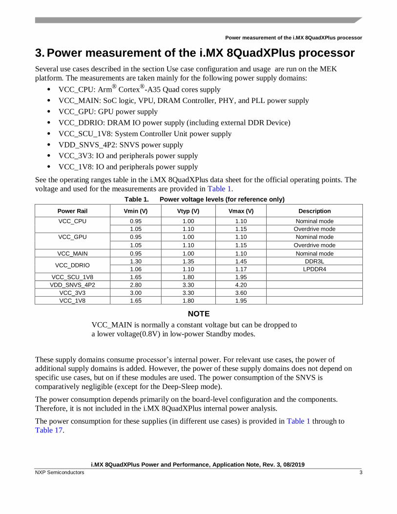
3. Power measurement of the i.MX 8QuadXPlus processor
Several use cases described in the section Use case configuration and usage are run on the MEK
platform. The measurements are taken mainly for the following power supply domains:
• VCC_CPU: Arm®
Cortex®
-A35 Quad cores supply
• VCC_MAIN: SoC logic, VPU, DRAM Controller, PHY, and PLL power supply
• VCC_GPU: GPU power supply
• VCC_DDRIO: DRAM IO power supply (including external DDR Device)
• VCC_SCU_1V8: System Controller Unit power supply
• VDD_SNVS_4P2: SNVS power supply
• VCC_3V3: IO and peripherals power supply
• VCC_1V8: IO and peripherals power supply
See the operating ranges table in the i.MX 8QuadXPlus data sheet for the official operating points. The
voltage and used for the measurements are provided in Table 1.
Table 1. Power voltage levels (for reference only)
Power Rail Vmin (V) Vtyp (V) Vmax (V) Description
VCC_CPU 0.95 1.00 1.10 Nominal mode
1.05 1.10 1.15 Overdrive mode
VCC_GPU 0.95 1.00 1.10 Nominal mode
1.05 1.10 1.15 Overdrive mode
VCC_MAIN 0.95 1.00 1.10 Nominal mode
VCC_DDRIO 1.30 1.35 1.45 DDR3L
1.06 1.10 1.17 LPDDR4
VCC_SCU_1V8 1.65 1.80 1.95
VDD_SNVS_4P2 2.80 3.30 4.20
VCC_3V3 3.00 3.30 3.60
VCC_1V8 1.65 1.80 1.95
NOTE
VCC_MAIN is normally a constant voltage but can be dropped to
a lower voltage(0.8V) in low-power Standby modes.
These supply domains consume processor’s internal power. For relevant use cases, the power of
additional supply domains is added. However, the power of these supply domains does not depend on
specific use cases, but on if these modules are used. The power consumption of the SNVS is
comparatively negligible (except for the Deep-Sleep mode).
The power consumption depends primarily on the board-level configuration and the components.
Therefore, it is not included in the i.MX 8QuadXPlus internal power analysis.
The power consumption for these supplies (in different use cases) is provided in Table 1 through to
Table 17.

Power measurement of the i.MX 8QuadXPlus processor
i.MX 8QuadXPlus Power and Performance, Application Note, Rev. 3, 08/2019
4 NXP Semiconductors
NOTE
Unless stated otherwise, all measurements were taken on a typical process
silicon, at a room temperature (approximately 25 °C). The power data
were measured under a controlled thermal tester. The power consumption
results under temp vary across silicon corners and may not reflect final
qualified silicon.
`cat /sys/class/thermal/thermal_zone0/temp` was used to log die
temperature, during the benchmark run
3.1. VCC_SCU_1V8 power
The VCC_SCU_1V8 voltage domain is generated from the PMIC. This domain powers the following
circuits:
• On-chip oscillators (OSC24M)
• eFuse power supplies
• Analog part of the PLLs
Temperature sensor
3.2. VCC_DDRIO power
The DDR I/O is supplied from the VCC_DDRIO which provides the power for the DDR I/O pads. The
target voltage for this supply depends on the DDR interface used. The target voltages for the different
DDR interfaces are as follows:
• 1.35 V for DDR3L
• 1.1 V for LPDDR4
The power consumption for the VCC_DDRIO supply is affected by various factors, including the
following:
• The amount of activity on the DDR interface.
• On-Die Termination (ODT): enabled/disabled, termination value, which is used for the DDR
controller and the DDR memories.
• The board termination for the DDR control and the address bus.
• The configuration of the DDR pads (such as the drive strength).
• The board layout.
• The load of the DDR memory devices.
NOTE
Due to the factors specified in the previous paragraph, the
measurements provided in the following tables vary from one
system to another. The provided data is for guidance only and
should not be treated as a specification.

Power measurement of the i.MX 8QuadXPlus processor
i.MX 8QuadXPlus Power and Performance, Application Note, Rev. 3, 08/2019
NXP Semiconductors 5
The measured current on the MEK Platform also includes the
current of the onboard LPDDR4 memory devices.
3.3. VCC_CPU/VCC_GPU/VCC_MAIN power
The voltage levels of all the supplies (except for VCC_CPU, VCC_GPU, VCC_MAIN) are set to the
typical voltage levels, as defined in the i.MX 8QuadXPlus Automotive and Infotainment Application
Processor (document IMX8QuadXPlusAEC).
The VCC_CPU, VCC_GPU, VCC_MAIN supplies require a special explanation. To save power, these
power voltages are changed during the runtime of the use cases. VCC_CPU and VCC_GPU can be
reduced based on frequency of the relevant core or powered completely off during low-power modes.
VCC_MAIN is normally a constant voltage but can be dropped to a lower voltage in low-power Standby
modes.
The target voltage levels for the VCC_CPU can vary to different mode according to the use cases.
Nominal allows a lower frequency for the core than the overdrive mode. There are several factors that
contribute to the mode decisions, with the performance required from the module being the most
important. The other factors are module latency requirements, thermal restrictions, and peripheral I/O
performance requirements.
NOTE
See the operating ranges table in the i.MX 8QuadXPlus Automotive and
Infotainment Application Processor (document IMX8QuadXPlusAEC) for
the official operating points.
Most of the measurements are performed using a combination of these voltage levels, and the power
data that appears in this document is according to these values. If the measurement is done at different
voltage levels, the power consumption scales with the voltage and the frequency change of the module
change. In real applications, the software (in conjunction with the hardware) automatically adjusts the
voltage and frequency values based on the use case requirements.
The voltage used for the power calculation is often an average voltage between those set-points. It
depends on the amount of time spent at each set-point.
3.4. Temperature measurements
In some use cases, the die temperature will not be enforced, but will simply be measured. The
temperature measurements were taken using the on-chip temperature sensor. While measuring the
temperature, it is recommended to wait until the temperature stabilizes.
NOTE
The measured temperatures are for reference only and vary on different
systems due to the differences in board, enclosure, and heat spreading
techniques. When using the same board type, the measured temperature
may vary due to factors such as the environment, silicon variations, and
measurement errors.

Use cases and measurement results
i.MX 8QuadXPlus Power and Performance, Application Note, Rev. 3, 08/2019
6 NXP Semiconductors
3.5. Hardware and software used
The software versions used for the measurements are as follows:
• Yocto rootfs, Linux Kernel version: L4.14.78 GA.
• The board used for the measurements is the i.MX 8QuadXPlus MEK Rev.C platform with B0
typical chip.
• The i.MX 8QuadXPlus MEK platform has been modified physically from its standard
configuration in order to measure individual power rails into the processor. A stock i.MX
8QuadXPlus MEK platform does not include these modifications.
• The measurements were performed using the Keysight34470A 6½ Digital Multimeter.
3.6. Measuring points on the MEK platform
Measure the power on a stock MEK platform requires rework.
CAUTION
NXP cannot be held responsible for damage to the board during a rework and unless properly done,
these reworks may render the board unusable.
In the MEK there is no shunt resister left for directtesting, all the power rails need to be reworked to be
measured. Lift one side (Pin1, not Pin2) of the inductor and add a shunt in series. You can solder an 0.02
Ω resistor (shunt). The tolerance of the 0.02 Ω resistors you use should be 1 %. Please refer to the MEK
design file from MEK Design Files.The measuring points for the various supply domains are as follows:
• VCC_CPU: The A35 Arm complex current is measured on the shunt. Lift the pin1 of L7 and add
shunt to the pad for test.
• VCC_MAIN: The chip domain current is measured on the shunt. There are two power rails to
supply VCC_MAIN, lift the pin1 of L1 and L2 and add shunt separately to the pad for test. The
total VCC_MAIN current is the sum of these two rails.
• VCC_GPU: The GPU current is measured on the shunt. Lift the pin1 of L4 and add shunt to the
pad for test.
• VCC_DDRIO: The DDRIO current contains QXP DDRIO and DRAM(except VCC_1V8 IO
rail) is measured on the shunt. Lift the pin1 of L6 and add shunt to the pad for test.
• VCC_SCU_1V8: Cut the trace between C135 and U8 pin 15 and add shunt for test.
• VCC_3V3: Lift the pin1 of L3 and add shunt to the pad for test.
• VCC_1V8: Lift the pin1 of L5 and add shunt to the pad for test.
4. Use cases and measurement results
The main use cases and subtypes, which form the benchmarks for the i.MX 8QuadXPlus internal power
measurements on the MEK platform, are:
• Low-power mode power consumption (Key States or ‘KS’)
— KS0 (SNVS-Only Mode)

Use cases and measurement results
i.MX 8QuadXPlus Power and Performance, Application Note, Rev. 3, 08/2019
NXP Semiconductors 7
— KS1 (Standby mode)
— KS2 (System IDLE with no screens active)
— KS3 (System idle with display on)
• Complex use case power consumption (Arm Core, GPU active)
— CoreMark (Arm Core only)
— Kanzi Performance Analyzer (GPU only)
— Kanzi Performance Analyzer (KPA) + 4 CoreMarks (Arm Core + GPU active)
• SOC subsystem performance benchmarks
— Core and memory benchmarks
— Storage I/O (Block and filesystem)
— GPU performance tests
— VPU performance tests
• Basicpower tests
— GPU power results
— Storage I/O power results
— Audio power results
4.1. Low-power mode power consumption (Key States or ‘KS’)
The use-case scenarios that have been tested are:
• KS0 (SNVS-Only mode)
• KS1 (Standby mode)
• KS2 (System idle with no screens)
• KS3 (System idle with display on)
4.1.1. KS0 – SNVS-Only mode
The use case is as follows.
• Only SNVS has active voltage. All other supplies off
This state represents the long-term power off state, where only the RTC and SNVS battery backed up
state is retained. All supplies except for the supply to the SNVS regulator are off. Only the SNVS pins
are active, other pins are OFF 32 K clock is running and RTC time is being kept (and an RTC wake-up
can occur) or the on-key can be asserted to cause the device to start up.
Resumption is via a full reboot, performing load of all code and full checking of state.
Table 2 show the measurement results when this use case is applied on the i.MX 8QXP processor.

Use cases and measurement results
i.MX 8QuadXPlus Power and Performance, Application Note, Rev. 3, 08/2019
8 NXP Semiconductors
Table 2. KS0 SNVS-Only Mode-External 32 Khz crystal — 25 ˚C
Supply domain
Voltage (V)
L4.14.78 GA
I (μA) P (μW)
VCC_CPU 0 0 0
VCC_MAIN 0 0 0
VCC_GPU 0 0 0
VCC_DDRIO 0 0 0
VDD_SNVS_4P2 4.20 3.37 14.15
VCC_SCU_1V8 0 0 0
Total SoC — — 14.15
VCC_1V8 0 0 0
VCC_3V3 0 0 0
Total SoC W/ IOs+Peripheral — — 14.15
4.1.2. KS1 – Standby mode
Here various RAMs on the device retain state, to allow a restart without a full reboot. The Logic state is
lost (or stored to RAMs via software) but the IOs are powered up, the GPIO will enter Open Drain and
maintaining their last state set (Pull-Up/Down). The external DDR is in self-refresh state.
Note that the IOs are added separately in the power measurements as they also supply some of the
platform’s components on the MEK’s design. Assumption is that all are static and consume relatively
low power (For example, no contention or low-resistance pullup).
The various PHYs are in Idle states, which in general means powered up at least partly but quiescent.
Only the 32 K XTAL is running (24 MHz and all PLL/ring OSC are powered down), analog
components are in the “off state”
The CPU and GPU supplies are all off and the main supply is dropped to 0.8 V nominal via the standby
mechanism.
Resumption is via a wake-up event, which causes a warm boot. In a warm boot the SCU resumes its
stored code (which need not be reauthenticated) using a special path which causes the various
subsystems to be reinitialized and the cores to start from stored program state in the DRAM.
DRAM must be retrained before we resume using it (by the SCU). KS1 may be seen as an equivalent of
the ACPI “Standby mode/sleep state” or S3 state(Suspend-to-RAM).
Table 3 show the measurement results when this use case is applied on the i.MX 8QuadXPlus processor.
Table 3. S1 standby mode — 25 ˚C
Supply domain
Voltage (V)
L4.14.78 GA
I (mA) P (mW)
VCC_CPU 0 0 0
VCC_MAIN 0.80 8.15 6.56
VCC_GPU 0 0 0

Use cases and measurement results
i.MX 8QuadXPlus Power and Performance, Application Note, Rev. 3, 08/2019
NXP Semiconductors 9
VCC_DDRIO 1.10 5.00 5.50
VCC_SCU_1V8 1.81 0.75 1.35
Total SoC — — 13.32
VCC_1V8 1.81 5.72 10.33
VCC_3V3 3.28 17.95 58.87
Total SoC W/ IOs+Peripheral — — 82.52
4.1.3. KS2 – System idle
The use case is as follows:
• Linux is idle mostly waiting for interrupt.
• 1 CPU powered, no GPU powered.
• Screen is off so no significant I/O to DDR is occurring
This is a short-term idle, the system has been running and can resume immediately based on an
interrupt from a timer or a peripheral. The PLLs and analog functions are all enabled and in “run
mode”. Voltage is set at 1.0 V nominal and the CPUis powered up.
This implies that the display is blank and no IO traffic is proceeding to the display interface, the
CPUs are statistically mostly idle or Off and waiting to resume.
The intent here is that the system reaches this state automatically, that is, the different components
detect the fact that they are idle (this is something which needs to be determined by a combination of
the different SW components and hardware but coordinated by the SCU) and then proceed to reach
the lowest low-power state that they can achieve without violating the response time. This differs
from Key state1 which requires an overall decision to enter a long-term idle.
Unlike the Key state 1 most of the system is actually at some level “active” so there is much
potential variation as to what exactly is enabled, thus it is an arbitrary definition for any one case.
Conceptually there are four states for each peripheral.
• OFF powered off, not initialized.
• SW gated, powered up and potentially initialized, SCU Firmware has turned off the clock so the
device is “offline”. May be looking for a wake-up event.
• Auto gated, initialized and gated to the extent that HW can determine, in effect functional, and
“online”. Will resume without SCU or SW action.
• ON, Actually active.
For purposes of measurement the following state is defined.
Subsystem State
GPU0 OFF
VPU OFF
DC0 OFF
DB Auto Clock gated, SSI to off subsystems SW gated
DRC#0 Auto clock gated, DDR in self-refresh power down
HSIO OFF, PCIe PHY in active mode for wake-up event

Use cases and measurement results
i.MX 8QuadXPlus Power and Performance, Application Note, Rev. 3, 08/2019
10 NXP Semiconductors
Connectivity SW clock gated, devices configured, looking for wake-up event
LSIO Auto clock gated, QSPI is idle
M4#0 ON, code loaded, WFI
SCU ON, code loaded, WFI
ADMA(QXP) Auto gated, DSP off, DSP RAM off, most peripherals SW gated, Interrupt active
DSI/LVDS # 0,1 SW gated, i2c maybe active looking for touch screen
CSI # 0 OFF
A35 core 0 WFI L1 coherent
A35 core 1-3 OFF (hot plugged)
A35 L2 WFI coherent retaining state
DRAM state
The DRAM is in self-refresh with its PLLs shutdown. The data is retained but resumption will take
around 20 μs. Periodic calibration should be carried out by the SCU code to avoid a full recalibration at
end of period.
Table 4 show the measurement results when this use case is applied on the i.MX 8QXP processor.
Table 4. KS2 system idle with no screens — 25˚C
Supply domain
Voltage (V)
L4.14.78 GA
I (mA) P (mW)
VCC_CPU 1.00 36.27 36.27
VCC_MAIN 1.02 478.93 488.51
VCC_GPU 1.10 6.94 7.64
VCC_DDRIO 1.10 93.43 103.98
VCC_SCU_1V8 1.79 25.08 45.00
Total SoC — — 681.4
VCC_1V8 1.81 62.11 112.90
VCC_3V3 3.28 17.50 57.42
Total SoC W/ IOs+Peripheral — — 851.72
4.1.4. KS3 System idle with display on
This is the state where the OS is fully running, with a display active and waiting for a command on the
GUI. No applications are running, only UI content is generated for display so very limited graphics but
some display.
The use case is as follows:
• Linux is operating, command prompt with the Weston window manager/compositor.
• Both CPU and GPU complexes are powered but IDLE.
• Screenis on.
Table 5 show the measurement results when this use case is applied on the i.MX 8QuadXPlus processor.

Use cases and measurement results
i.MX 8QuadXPlus Power and Performance, Application Note, Rev. 3, 08/2019
NXP Semiconductors 11
Table 5. KS3 - System idle with display on — 25 ˚C
Supply domain
Voltage (V)
L4.14.78 GA
I (mA) P (mW)
VCC_CPU 1.00 20.36 20.47
VCC_MAIN 1.06 568.49 600.42
VCC_GPU 1.10 7.38 8.12
VCC_DDRIO 1.12 138.93 155.55
VCC_SCU_1V8 1.83 27.39 49.24
Total SoC — — 833.79
VCC_1V8 1.83 11.00 201.14
VCC_3V3 3.28 17.61 57.76
Total SoC W/ IOs+Peripheral — — 1092.68
NOTE
For additional details about this use case and settings, see Use case
configuration and usage guidelines.
4.2. Complex use case power consumption (Arm Core, GPU active)
The use-case scenarios for Performance Modes, utilizing both the CPU and GPU that have been tested
are:
• CoreMark only
• Kanzi Performance Analyzer (KPA) only
• KPA and 4 Coremark
4.2.1. CoreMark only
CoreMark is a modern, sophisticated benchmark that lets you accurately measure processor performance
and is intended to replace the older Dhrystone benchmark. Arm recommends using CoreMark in
preference to Dhrystone.
In this test a single instance of CoreMark is running on one Cortex A core.
For best performances compile with:
-O2 -DMULTITHREAD=4 -DUSE_PTHREAD -lpthread -O3 -funroll-all-loops
--param max-inline-insns-auto=550 -ftracer -falign-jumps=16 -ftree-loop-im -fivopts
-ftree-loop-ivcanon -fvect-cost-model -fvariable-expansion-in-unroller
--param max-unrolled-insns=999999 --param max-average-unrolled-insns=99999999
--param iv-max-considered-uses=9999999 --param iv-consider-all-candidates-bound=99999
--param iv-always-prune-cand-set-bound=999999 -fmodulo-sched
-fmodulo-sched-allow-regmoves -fgcse-lm -fgcse-sm -fgcse-las -funsafe-loop-optimizations
-freschedule-modulo-scheduled-loops -ftree-vectorize -DPERFORMANCE_RUN=1 -lrt

Use cases and measurement results
i.MX 8QuadXPlus Power and Performance, Application Note, Rev. 3, 08/2019
12 NXP Semiconductors
• CPU frequency is set to maximum value
• DDR frequency is set to 1200 MHz
Table 6 show the measurement results when this use case is applied on the i.MX 8QuadXPlus processor.
Table 6. CoreMark only — 25 0C
Supply domain
Voltage (V)
L4.14.78 GA
I (mA) P (mW)
VCC_CPU 1.10 447.18 491.90
VCC_MAIN 1.02 477.14 486.68
VCC_GPU 1.10 7.25 7.99
VCC_DDRIO 1.11 93.82 104.40
VCC_SCU_1V8 1.79 25.10 45.05
Total SoC — — 1136.02
VCC_1V8 1.82 62.43 113.44
VCC_3V3 3.28 16.33 53.56
Total SoC W/ IOs+Peripheral — — 1303.01
4.2.2. Kanzi performance analyzer only
Kanzi Performance Analyzer (KPA) is a Human Machine Interface (HMI) benchmarking tool from
RightWare.
It is primarily focused on automotive Human Machine Interfaces such as Cluster, Heads up Displays,
Infotainment screens but is an excellent tool for measuring the performance and power consumption for
any generic HMI tool.
Kanzi Performance Analyzer is available from Rightware (www.rightware.com)
In this use case only KPA is running on the GPU. No workloads are executing on the main Cortex A
cores (or any other IP block). This emulates a heavy GPU-specific use case and associated power
consumption.
Table 7 show the measurement results when this use case is applied on the i.MX 8QuadXPlus processor.
Table 7. Kanzi only — 25 0C
Supply domain
Voltage (V)
L4.14.78 GA
I (mA) P (mW)
VCC_CPU 1.10 141.70 155.86
VCC_MAIN 1.02 937.31 956.06

SOC subsystem performance tests
i.MX 8QuadXPlus Power and Performance, Application Note, Rev. 3, 08/2019
NXP Semiconductors 13
VCC_GPU 1.10 404.65 445.11
VCC_DDRIO 1.10 413.08 454.39
VCC_SCU_1V8 1.80 27.24 48.96
Total SoC — — 2060.38
VCC_1V8 1.83 113.64 208.10
VCC_3V3 3.28 16.29 53.42
Total SoC W/ IOs+Peripheral — — 2321.92
4.2.3. Kanzi performance analyzer and 4 CoreMarks
For this test, KPA is running on the GPU and 4 instances of CoreMark are running on the Cortex A
cores to emulate a heavy application workload.
Table 8 show the measurement results when this use case is applied on the i.MX 8QuadXPlus
processor.
Table 8. Kanzi and 4 CoreMark — 25 0C
Supply domain
Voltage (V)
L4.14.78 – GA
I (mA) P (mW)
VCC_CPU 1.12 447.67 492.44
VCC_MAIN 1.02 753.16 768.23
VCC_GPU 1.10 199.22 219.14
VCC_DDRIO 1.11 253.72 279.09
VCC_SCU_1V8 1.80 27.31 49.09
Total SoC — — 1807.98
VCC_1V8 1.83 111.35 203.78
VCC_3V3 3.28 15.49 50.83
Total SoC W/ IOs+Peripheral — — 2062.58
5. SOC subsystem performance tests
The following use cases measure the performance of the SOC’s main cores, DDR traffic, GPU, and
Storage I/O utilizing many industry-standard benchmarks.
The performance results listed here were run on nominal silicon and frequencies for the major IP blocks
are assumed at maximum unless otherwise specified.

SOC subsystem performance tests
i.MX 8QuadXPlus Power and Performance, Application Note, Rev. 3, 08/2019
14 NXP Semiconductors
5.1. Core and memory benchmarks
Table 9. Core and memory benchmarks
Benchmark Performance Metric
Coremark 13933.78 Iter/sec
2.90 Coremark/MHz
Dhrystone
2781.9 DMIPS
2.324 DMIPS/MHz
C-ray 330 milliseconds
Stream 5107 MB/s
LMBench (L1 latency) 2.538 ns
LMBench (L2 latency) 7.18 ns
Whetstone SP 959 WMIPS
Mem/memset 6881 MB/s
Mem/memcpy 1596.621 MB/s
5.2. Storage I/O
DD was used for block level testing and Iozone benchmark for file system level testing.
5.2.1. Block level testing
Table 10. Block level
Component measured Performance Metric
SanDisk Extreme SD C10, U3, V30 write 59.70 MB/s
SanDisk Extreme SD C10, U3, V30 read 93.50 MB/s
Kingston DataTraveler Elite G2 write 95.60 MB/s
Kingston DataTraveler Elite G2 read 231.00 MB/s
Samsung SSD 850 EVO write 83.2 MB/s
Samsung SSD 850 EVO read 240.00 MB/s
eMMC write 78.80 MB/s
eMMC read 283.00 MB/s
5.2.2. File system level testing
Table 11. File system level
Component measured Performance Metric
SanDisk Extreme SD C10, U3, V30 write 66.662 MB/s
SanDisk Extreme SD C10, U3, V30 read 112.836 MB/s
Kingston DataTraveler Elite G2 write 113.992 MB/s
Kingston DataTraveler Elite G2 read 251.319 MB/s
Samsung SSD 850 EVO write 184.332 MB/s
Samsung SSD 850 EVO read 229.356 MB/s
eMMC write 79.473 MB/s
eMMC read 324.058 MB/s

Basic power tests
i.MX 8QuadXPlus Power and Performance, Application Note, Rev. 3, 08/2019
NXP Semiconductors 15
5.3. GPU performance tests
The following additional GPU performance tests were run.
5.3.1. GLMARK2
Table 12. Glmark2 is an OpenGL 2.0 and ES 2.0 benchmark.GLMARK2
Phase Performance Metric
Windowed 737.67 Score
Full screen 436 Score
5.3.2. Kanzi performance analyzer
Table 13. Kanzi performance analyzer
Phase Performance Metric
Digital Cockpit 228 Score
Car Shading 195 Score
Fast Cluster 423 Score
5.4. VPU performance tests
Table 14. VPU
Algorithm File Performance Metric
Playback (gstlaunch-
1.0)
HEVC_1920x1080_29.97fps_AACLC_44.1Khz_
2ch.mkv
30.10 FPS
HEVC_1920x1080_60fps_AACLC_48Khz_6ch_
cfg06.mkv
59.53 FPS
Playback (Gplay-1.0) HEVC_1920x1080_29.97fps_AACLC_44.1Khz_
2ch.mkv
30 FPS
HEVC_1920x1080_60fps_AACLC_48Khz_6ch_
cfg06.mkv
58.79 FPS
Playback + GUI
gplay-1.0
HEVC_1920x1080_29.97fps_AACLC_44.1Khz_
2ch.mkv video-sink=”kmssink sync=false”
29.81 FPS
+tutorial3_es20 -f 600* 30.9
gplay-1.0
HEVC_1920x1080_60fps_AACLC_48Khz_6ch_
cfg06.mkv video-sink=”kmssink sync=false”
59.601 FPS
+ /tutorial3_es20 -f 600* 30.79
*tutorial3_es20 is an OpenGL demo.
6. Basic power tests
This section provides the GPU power results, storage I/O power results, and audio power results.
Reducing power consumption
i.MX 8QuadXPlus Power and Performance, Application Note, Rev. 3, 08/2019
16 NXP Semiconductors
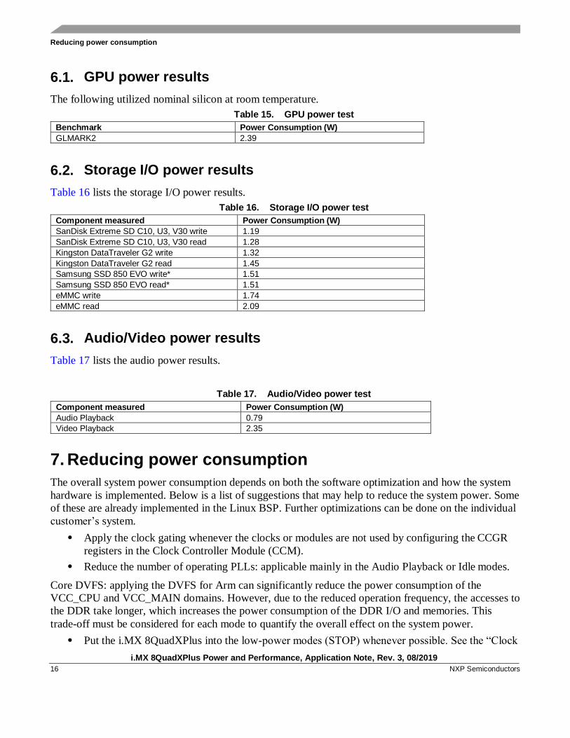
6.1. GPU power results
The following utilized nominal silicon at room temperature.
Table 15. GPU power test
Benchmark Power Consumption (W)
GLMARK2 2.39
6.2. Storage I/O power results
Table 16 lists the storage I/O power results.
Table 16. Storage I/O power test
Component measured Power Consumption (W)
SanDisk Extreme SD C10, U3, V30 write 1.19
SanDisk Extreme SD C10, U3, V30 read 1.28
Kingston DataTraveler G2 write 1.32
Kingston DataTraveler G2 read 1.45
Samsung SSD 850 EVO write* 1.51
Samsung SSD 850 EVO read* 1.51
eMMC write 1.74
eMMC read 2.09
6.3. Audio/Video power results
Table 17 lists the audio power results.
Table 17. Audio/Video power test
Component measured Power Consumption (W)
Audio Playback 0.79
Video Playback 2.35
7. Reducing power consumption
The overall system power consumption depends on both the software optimization and how the system
hardware is implemented. Below is a list of suggestions that may help to reduce the system power. Some
of these are already implemented in the Linux BSP. Further optimizations can be done on the individual
customer’s system.
• Apply the clock gating whenever the clocks or modules are not used by configuring the CCGR
registers in the Clock Controller Module (CCM).
• Reduce the number of operating PLLs: applicable mainly in the Audio Playback or Idle modes.
Core DVFS: applying the DVFS for Arm can significantly reduce the power consumption of the
VCC_CPU and VCC_MAIN domains. However, due to the reduced operation frequency, the accesses to
the DDR take longer, which increases the power consumption of the DDR I/O and memories. This
trade-off must be considered for each mode to quantify the overall effect on the system power.
• Put the i.MX 8QuadXPlus into the low-power modes (STOP) whenever possible. See the “Clock

Use case configuration and usage guidelines
i.MX 8QuadXPlus Power and Performance, Application Note, Rev. 3, 08/2019
NXP Semiconductors 17
Controller Module (CCM)” chapter in the i.MX 8QuadXPlus Applications Processor Reference
Manual (document IMX8QuadXPlusRM) for details.
• DDR interface optimization:
— Employ careful board routing of the DDR memories, maintaining the PCB trace lengths
as short as possible.
— Use as reduced an ODT (On-Die Termination) setting as possible. The termination used
greatly influences the power consumption of the DDR interface pins.
— Use a proper output driver impedance for the DDR interface pins that provide good
impedance matching. Select the lowest possible drive strength that provides the required
performance to reduce the current flowing through the DDR I/O pins.
— In the lower-performance use cases, switching to the DLL Off mode greatly reduces the
DDR frequency. This disable or reduces the termination, and reduces the drive strength.
Thus, the power consumption of the DDR interface pins can be reduced significantly.
— Float the i.MX 8QuadXPlus DDR interface pins (set to high Z) when the DDR memory is
in the Self-Refresh mode, and keep DDR_SDCKE0 and DDR_SDCKE1 at a low value. If
DDR_SDCKE0 and DDR_SDCKE1 are kept at a low value using external pull-down
resistors, make sure that there is no onboard termination on these pins during this mode.
— If possible (depending on the system stability), configure the DDR input pins to the
CMOS mode instead of the Differential mode. This can be done by clearing the
DDR_INPUT bit in the corresponding registers in the IOMUXC. This setting is mostly
recommended when operating at low frequencies, such as in the DLL Off mode.
— The use of the DDR memory offerings in the latest process technology can significantly
reduce the power consumption of the DDR devices and the DDR I/O.
The various steps involved in floating the i.MX 8QuadXPlus DDR interface pins are shown below.
8. Use case configuration and usage guidelines
This section describes the step of core and memory benchmarks.
8.1. Low-power mode configuration
• KS1
Echo mem > /sys/power/state
• KS2
Full boot without any screen connected, just one core online
• KS3
KS2 + screen connected

Use case configuration and usage guidelines
i.MX 8QuadXPlus Power and Performance, Application Note, Rev. 3, 08/2019
18 NXP Semiconductors
8.2. Core and memory benchmarks
8.2.1. System setup
1. SD boot.
2. Connect the display.
8.2.2. Steps – Coremark/Dhrystone/Stream/WhetstoneSP
1. Boot up theSystem.
2. Measure the maximum frequency.
#!/bin/sh
systemctl stop weston
echo 1 > /sys/class/graphics/fb0/blank;
cpufreq-set -g performance
3. Run coremark/dhrystone2/stream and measure.
4. Measure the power and record the result.
8.2.3. Steps – Memset/Memcpy
1. Boot up the System.
2. Measure the maximum frequency.
3. Run memset/memcpy and measure:
perf bench -f simple mem memset -s 1000MB
perf bench -f simple mem memcpy -s 1000MB
4. Measure the power and record the result.The time frame is 30s.
8.3. Storage I/O
This section lists steps for block-level storage I/O and file-system level storage I/O.
8.3.1. System setup
1. SD boot.
2. For USB/SSD – connect the desired device to your board.

Use case configuration and usage guidelines
i.MX 8QuadXPlus Power and Performance, Application Note, Rev. 3, 08/2019
NXP Semiconductors 19
8.3.2. Steps – Block-level storage I/O – dd
DD_RD_SDCARD
1. Run dd_read script on SD card (see below).
2. Start power measurement and record data.
#!/bin/bash
# Since we’re dealing with dd, abort if any errors occur
set -e
TEST_FILE=${1:-dd_ibs_testfile}
#if [ -e “$TEST_FILE” ]; then TEST_FILE_EXISTS=$?; fi
#TEST_FILE_SIZE=3221225472
#134217728
# Exit if file exists
#if [ -e $TEST_FILE ]; then
# echo “Test file $TEST_FILE exists, aborting.”
# exit 1
#fi
#TEST_FILE_EXISTS=1
if [ $EUID -ne 0 ]; then
echo “NOTE: Kernel cache will not be cleared between tests without sudo. This will
likely cause inaccurate results.” 1>&2
fi
# Create test file
#echo ‘Generating test file...’
#BLOCK_SIZE=65536
#COUNT=$(($TEST_FILE_SIZE / $BLOCK_SIZE))
#dd if=/dev/urandom of=$TEST_FILE bs=$BLOCK_SIZE count=$COUNT conv=fsync > /dev/null
2>&1
# Header
PRINTF_FORMAT=”%8s : %s\n”
printf “$PRINTF_FORMAT” ‘block size’ ‘transfer rate’
# Block sizes of 512b 1K 2K 4K 8K 16K 32K 64K 128K 256K 512K 1M 2M 4M 8M 16M 32M 64M
for BLOCK_SIZE in 512 1024 2048 4096 8192 16384 32768 65536 131072 262144 524288
1048576 2097152 4194304 8388608 16777216 33554432 67108864
do
# Clear kernel cache to ensure more accurate test
[ $EUID -eq 0 ] && [ -e /proc/sys/vm/drop_caches ] && echo 3 >
/proc/sys/vm/drop_caches
# Read test file out to /dev/null with specified block size
DD_RESULT=$(dd if=$TEST_FILE of=/dev/null bs=$BLOCK_SIZE 2>&1 1>/dev/null)
# Extract transfer rate

Use case configuration and usage guidelines
i.MX 8QuadXPlus Power and Performance, Application Note, Rev. 3, 08/2019
20 NXP Semiconductors
TRANSFER_RATE=$(echo $DD_RESULT | \grep –only-matching -E ‘[0-9.]+
([MGk]?B|bytes)/s(ec)?’)
printf “$PRINTF_FORMAT” “$BLOCK_SIZE” “$TRANSFER_RATE”
done
DD_WRT_SDCARD
1. Run dd_write script on SD card (see below).
2. Start power measurement and record data.
DD_RD_eMMC
1. Run dd_read script on eMMC partition card (see section 8.3.2.1).
2. Start power measurement and record data.
DD_WRT_eMMC
1. Run dd_write script on eMMC partition card (see section 8.3.2.2).
2. Start power measurement and record data.
8.3.3. File system-level I/O – iozone
This section lists steps for SDHC class 10, eMMC, and USB3.0 storage.
IO_WRT_SDCARD
1. Run iozone on SD card (you may create a loop for continuous power measurement).
./iozone -i 0 -b /tmp/iozone.xls -r 128k -s 3G -l 1 -u 1
Iozone generates and measures read (-I 0) file operations; the benchmark was ran using a file size of 3G
(-s 3G) and record size of 128k (-r 128k) on a single core (-u 1).
2. Start power measurement and record data.
IO_WRT_eMMC
1. Run iozone on SD card (you may create a loop for continuous power measurement)
./iozone -i 0 -b /tmp/iozone.xls -r 128k -s 3G -l 1 -u 1
2. Start power measurement and rrecord data

Use case configuration and usage guidelines
i.MX 8QuadXPlus Power and Performance, Application Note, Rev. 3, 08/2019
NXP Semiconductors 21
Storage – USB3.0
8.3.3.3.1. DD_RD_USB3.0
1. Run dd_read script on USB 3.0 partition card (see section 8.3.2.1).
2. Start power measurement and record data.
8.3.3.3.2. DD_WRT_USB3.0
1. Run dd_write script on USB 3.0 partition card (see section 8.3.2.2).
2. Start power measurement and record data.
8.3.3.3.3. IO_WRT_USB3.0
1. Run iozone on USB 3.0 card (you may create a loop for continuous power measurement).
./iozone -i 0 -b /tmp/iozone.xls -r 128k -s 3G -l 1 -u 1
2. Start power measurement and record data.
8.4. GPU performance tests
8.4.1. System setup
1. SD boot.
2. Connect the HDMI monitor.
3. For USB/SSD – connect the desired device to your board.
8.4.2. Kanzi + 4 Coremark
1. Boot up the Linux image and boot the board to the SD roots.
2. measure the maximum frequency, run the following script. #!/bin/sh
ifconfig eth0 down ifconfig eth1 down
systemctl start eston
echo 0 > /sys/class/graphics/fb0/blank;
cpufreq-set -g performance
3. Run in a loop.
First script
#!/bin/bash
echo -e „\033[9;0]“ > /dev/tty0
cd KPA_1_0_1_137/linux_wayland_aarch64
export LD_LIBRARY_PATH=”$PWD”
while true; do
./kpa.exe
Use case configuration and usage guidelines
i.MX 8QuadXPlus Power and Performance, Application Note, Rev. 3, 08/2019
22 NXP Semiconductors
done
second script
#!/bin/bash
while true ; do taskset -c 0 ./coremark_4.exe 0x0 0x0 0x66 0 7 1 2000 ; done &
while true ; do taskset -c 1 ./coremark_4.exe 0x0 0x0 0x66 0 7 1 2000 ; done &
while true ; do taskset -c 2 ./coremark_4.exe 0x0 0x0 0x66 0 7 1 2000 ; done &
while true ; do taskset -c 3 ./coremark_4.exe 0x0 0x0 0x66 0 7 1 2000 ; done &
4. Start power measurement and record the result.
8.4.3. Active use case
1. Boot up the Linux image and boot the board to the SD roots.
2. To measure the maximum frequency, run the following script. #!/bin/sh
ifconfig eth0 down ifconfig eth1 down
systemctl start eston
echo 0 > /sys/class/graphics/fb0/blank;
cpufreq-set -g performance
3. Run in a loop. Main script
dhrystone_loop.sh &
memcpy_loop.sh &
g2d_loop.sh &
furshell.sh &
#move the cursor to the second screen and play the videoplayback
gplay_videoplayback.sh
dhrystone_loop.sh:
while [ “1” == “1” ]
do
taskset -c 0 /run/media/mmcblk1p3/8QXP_B0/dhry2 > dhry2_core0 &
taskset -c 1 /run/media/mmcblk1p3/8QXP_B0/dhry2 > dhry2_core1 &
taskset -c 2 /run/media/mmcblk1p3/8QXP_B0/dhry2 > dhry2_core2
memcpy_loop.sh
done
memcpy loop.sh
#!/bin/bash
while true;do
perf bench -f simple mem memcpy -l10000 -s 1024MB > memcpy_run.txt
done
g2d_loop.sh
#!/bin/bash
while true;do
/opt/g2d_samples/g2d_test > g2dtest_run.txt 2>&1
done
furshell_loop.sh
/opt/imx-gpu-sdk/GLES3/FurShellRendering/FurShellRendering_Wayland –LogStats –
LayerCount 100 > furshell_run.txt
gplay_videoplayback.sh

Revision history
i.MX 8QuadXPlus Power and Performance, Application Note, Rev. 3, 08/2019
NXP Semiconductors 23
!#/bin/bash
path=`pwd`
FILE=HEVC_1920x1080_29.97fps_AACLC_44.1Khz_2ch.mkv
#HEVC_3840x2160_60fps_AACLC_48Khz_6ch_cfg02.mkv
while true; do gplay-1.0 $path/$FILE > /dev/null ; done
4. Start power measurement and record the result.
8.5. VPU performance
This section list the steps for system setup and video playback with HDMI.
8.5.1. System setup
1. SD boot.
2. Connect the HDMI monitor.
8.5.2. Video playback with HDMI
1. Boot up the Linux image and boot the board to the SD rootfs.
2. To measure the maximum frequency, run the following script. #!/bin/sh
ifconfig eth0 down ifconfig eth1 down
systemctl start eston
echo 0 > /sys/class/graphics/fb0/blank;
cpufreq-set -g performance
/usr/bin/gst-launch-1.0 playbin uri=file://$PATH/$FILE video-sink=”kmssink sync=false”
3. Measure the power and record the result.
9. Revision history
Table 18 is the revision history table for the application note.
Table 18. Revision history
Revision number Date Substantive changes
0 02/2019 Initial release
1 05/2019 Updates on VCC and DDR
2 07/2019 Updated Section 5.3.2 Kanzi
performance analyzer
3 08/2019 Update Table 13

Document Number: AN12338 Rev. 3
08/2019
How to Reach Us:
Home Page:
nxp.com
Web Support:
nxp.com/support
Information in this document is provided solely to enable system and software implementers to
use NXP products. There are no express or implied copyright licenses granted hereunder to
design or fabricate any integrated circuits based on the information in this document. NXP
reserves the right to make changes without further notice to any products herein.
NXP makes no warranty, representation, or guarantee regarding the suitability of its products for
any particular purpose, nor does NXP assume any liability arising out of the application or use of
any product or circuit, and specifically disclaims any and all liability, including without limitation
consequential or incidental damages. “Typical” parameters that may be provided in NXP data
sheets and/or specifications can and do vary in different applications, and actual performance
may vary over time. All operating parameters, including “typicals,” must be validated for each
customer application by customer’s technical experts. NXP does not convey any license under its
patent rights nor the rights of others. NXP sells products pursuant to standard terms and
conditions of sale, which can be found at the following address: nxp.com/SalesTermsandConditions.
While NXP has implemented advanced security features, all products may be subject to
unidentified vulnerabilities. Customers are responsible for the design and operation of their
applications and products to reduce the effect of these vulnerabilities on customer’s applications
and products, and NXP accepts no liability for any vulnerability that is discovered. Customers
should implement appropriate design and operating safeguards to minimize the risks associated
with their applications and products.
NXP, the NXP logo, NXP SECURE CONNECTIONS FOR A SMARTER WORLD, COOLFLUX,
EMBRACE, GREENCHIP, HITAG, I2C BUS, ICODE, JCOP, LIFE VIBES, MIFARE, MIFARE
CLASSIC, MIFARE DESFire, MIFARE PLUS, MIFARE FLEX, MANTIS, MIFARE ULTRALIGHT,
MIFARE4MOBILE, MIGLO, NTAG, ROADLINK, SMARTLX, SMARTMX, STARPLUG, TOPFET,
TRENCHMOS, UCODE, Freescale, the Freescale logo, AltiVec, C‑5, CodeTEST, CodeWarrior,
ColdFire, ColdFire+, C‑Ware, the Energy Efficient Solutions logo, Kinetis, Layerscape, MagniV,
mobileGT, PEG, PowerQUICC, Processor Expert, QorIQ, QorIQ Qonverge, Ready Play,
SafeAssure, the SafeAssure logo, StarCore, Symphony, VortiQa, Vybrid, Airfast, BeeKit,
BeeStack, CoreNet, Flexis, MXC, Platform in a Package, QUICC Engine, SMARTMOS, Tower,
TurboLink, UMEMS, EdgeScale, EdgeLock, eIQ, and Immersive3D are trademarks of NXP B.V.
All other product or service names are the property of their respective owners. AMBA, Arm,
Arm7, Arm7TDMI, Arm9, Arm11, Artisan, big.LITTLE, Cordio, CoreLink, CoreSight, Cortex,
DesignStart, DynamIQ, Jazelle, Keil, Mali, Mbed, Mbed Enabled, NEON, POP, RealView,
SecurCore, Socrates, Thumb, TrustZone, ULINK, ULINK2, ULINK-ME, ULINK-PLUS, ULINKpro,
µVision, Versatile are trademarks or registered trademarks of Arm Limited (or its subsidiaries) in
the US and/or elsewhere. The related technology may be protected by any or all of patents,
copyrights, designs and trade secrets. All rights reserved. Oracle and Java are registered
trademarks of Oracle and/or its affiliates. The Power Architecture and Power.org word marks and
the Power and Power.org logos and related marks are trademarks and service marks licensed by
Power.org.
© 2018-2019 NXP B.V.