in-line fiber evanescent field electrooptic modulatorsarft/publications/jnopm_published.pdf ·...
TRANSCRIPT
Journal of Nonlinear Optical Physics & MaterialsVol. 9, No. 1 (2000) 79–94c©World Scientific Publishing Company
IN-LINE FIBER EVANESCENT FIELD
ELECTROOPTIC MODULATORS
CARL ARFT, DIEGO R. YANKELEVICH and ANDRE KNOESEN
Department of Electrical and Computer Engineering, University of California,Davis, CA 95616, USA
ERJI MAO and JAMES S. HARRIS JR.
Solid State and Photonics Laboratory, 329 CISX Building,Stanford University, Stanford, CA 94305, USA
Received 1 November 1999
Electrooptic modulators that consist of an optical fiber waveguide coupled to an elec-trooptic waveguide are reviewed. Desirable attributes of these devices are that the opticalfiber is uninterrupted and the interaction with the electrooptic region occurs only wherethe optical properties are modulated. In this paper we review in-line fiber evanescent fieldmodulators that we have implemented with electrooptic polymers and compound semi-conductor quantum wells. We show that the beam propagation method can accuratelysimulate the behavior measured in these devices.
1. Introduction
Efficient methods to modulate the optical carrier are important in large informa-
tion capacity fiberoptic links. The direct modulation of laser diodes is attractive,
but amplitude and phase distortions at high modulation frequencies become limiting
factors in digital and analog optical links. This and other limitations can be avoided
by modulating the optical carrier with external modulators. The properties of the
external modulators can be optimized independent of, and do not impose restric-
tions upon, the optical source. An in-depth review of wide-bandwidth lasers and
modulators has been published recently.1 Lithium niobate Mach–Zehnder interfero-
metric modulators are available commercially, but do not meet all of the demands of
high frequency optical communication channels. For such reasons, other approaches
to achieve high-speed modulation are of current research interest. For example, this
includes the development of new materials for Mach–Zehnder modulators, but
also other modulator geometries such as electroabsorption modulators, and coupler
modulators.
In this paper we are reviewing an electrooptic modulator that is based on in-
line optical modulators implemented on fiber half-couplers. A fiber half-coupler is a
device wherein a continuous optical fiber is modified so as to allow interaction with
79
80 C. Arft et al.
the propagating electric field. To modulate the transmittance of the optical fiber, an
electrooptic waveguide is deposited onto the half-coupler. When the modes in the
fiber and the electrooptic waveguide are close to phase-matching, coupling occurs
between the modes. By altering the refractive index of the electrooptic guide, the
phase matching condition is changed, resulting in the modulation of the electric
field in the fiber. As a modulator we will show this configuration has attractive
attributes, and it can take advantage of electrooptic polymers, compound semi-
conductor materials, and electrooptic crystals. After a short review of modulator
requirements, we show how in-line fiber modulators can meet the main requirements
of external modulators. The paper then discusses the electromagnetic interactions
present in this device, and shows that even though the interactions are more compli-
cated than in conventional interferometers and couplers, the performance of in-line
optical modulators can be precisely analyzed by the beam propagation method.
2. In-line Fiber Modulators
A high-speed electrooptic modulator must meet several requirements. For high fre-
quency performance, the velocities of the modes in the optical waveguide and high
frequency transmission line must be matched. This depends on the dispersive cha-
racteristics of the electrooptic material, as well as dispersive characteristics of the
optical waveguide and the high frequency transmission line. For example, lithium
niobate (LiNbO3) has a large velocity mismatch; however, for a LiNbO3 modulator,
the device dispersion can be minimized and the high frequency performance maxi-
mized by implementing a ridge waveguide2 on a thin substrate.3 Polymers have the
advantage of favorable material dispersion characteristics for the matching of optical
and high frequency modes, which simplifies high frequency modulator structures.4
The device must have low optical insertion loss. Traditional modulators couple
light from an optical fiber to a channel electrooptic waveguide. The mode shape
mismatch between the optical fiber and the channel waveguide, and Fresnel reflec-
tions introduce losses that can easily cause a 50% loss in optical power. Material
and scattering losses in the channel waveguide could also further contribute to the
insertion loss. In addition, semiconductor and nonlinear polymer materials may ex-
hibit absorption, which in addition to introducing excess loss also limits the power
handling capability of the modulator. For shot–noise limited detection of optical
signals, it is desirable to have large optical powers at the receiver, and the external
modulator ideally should be able to handle optical powers on the order of tens of
milliwatts. For these reasons it is desirable to have a device in which the optical
fiber is continuous and the interaction with the electrooptic material is only where
the optical properties are being modulated.
Modulation efficiency, phase distortion, and linearity are also important factors
in the device performance. In digital applications it is desirable to have 100% effi-
ciency with minimal phase distortions. Phase distortion can limit the maximum
distance between transmitter and receiver. In analog applications, linearity is of
In-line Fiber Evanescent Field Electrooptic Modulators 81
critical importance. Spurious distortions, introduced by nonlinearities of the modu-
lator transmittance transfer function (MTTF), can rise above the noise floor when
large input signals modulate the carrier. For this reason, fairly low modulation
efficiencies (e.g. 5%) can be acceptable for analog modulators.5 RF-photonic links
have a variety of attractive features for radar applications, but it is important that
the analog modulator has a large dynamic range. In a radar application, targets
are being tracked over large distances, and the amplitude of return signals must be
tracked over a very large range. The dynamic range is quantified by the spurious
free dynamic range (SFDR),6 which is defined as the difference between the largest
signal power before the distortions rise above the noise floor and the smallest signal
power that can be detected. As an illustration of the importance of the SFDR con-
sider the following example. A state-of-the-art high frequency amplifier can have a
SFDR of 80 dB-MHz2/3.7 The performance of a radar system utilizing this ampli-
fier will be compromised if a Mach–Zehnder electrooptic modulator is used. The
Mach–Zehnder modulator, which has a SFDR of approximately 72 dB-MHz2/3,8
will determine the system SFDR. To place these figures in perspective, a 10 dB dif-
ference in SFDR will reduce the radar range by a factor of two. A challenge to the
optical community is therefore to develop a new electrooptic modulator configura-
tion that has a SFDR comparable to electronic components. The in-line modulator
has the potential to provide a SFDR competitive with more complicated solutions
involving multiple Mach–Zehnder modulators.5
An in-line asymmetric directional coupler modulator (ADCM) is an asymmetric
directional coupler (ADC) consisting of two waveguides placed in close proxim-
ity. The two waveguides can be of dissimilar shape and/or material. In the in-line
ADCM, one of the waveguides is an optical fiber, and the other is an electroop-
tic waveguide. The difference in waveguide geometries does not prevent the phase
matching of modes in the two waveguides and a strong coupling between the fiber
and the electrooptic waveguide can exist. The ADCM configuration has several at-
tractive attributes. It is constructed with an uninterrupted optical fiber, resulting
in a low optical insertion loss. The basic building block of the in-line ADCM is
known as the half-coupler. It consists of a continuous optical fiber that is adhered
to a fused silica substrate or silicon v-groove, then the cladding is polished to close
proximity of the core. The fabrication method for the half-coupler implementation
was presented by Shaw et al.9 Passive devices with attenuating, polarizing and sens-
ing capabilities were commercially available a few years later.10 Research activities
focusing on active devices were initiated in the 1990’s by Creaney et al. with the
development of a modulator that uses LiNbO3 crystals.11 Recently DAST, an or-
ganic crystal, has also been used in an in-line modulator.12 In both instances it was
difficult to integrate the organic crystal onto the half-coupler.
Unlike conventional modulators, the interaction with the electrooptic region is
limited to only the region where the index is modulated. This permits the use
of electrooptic materials that would, for conventional waveguide modulators, have
unacceptably large absorption losses. We have demonstrated in-line modulators that

82 C. Arft et al.
use electrooptic polymer13 and compound semiconductor multiple quantum well
waveguides.14 The electrooptic properties of polymers and multilayered compound
semiconductors can be engineered towards specific device requirements. This ability
to tailor material properties has resulted in the demonstration of ultrawide band-
width13 and high modulation efficiency14 devices that still meet the low insertion
loss requirements.
We have demonstrated the feasibility of three types of external in-line modu-
lator configurations using commercially available half-coupler blocks.15 The inter-
action length in these half-couplers is limited to approximately a millimeter due
to the curvature of the fiber in the half-coupler block. The first device is a Fabry–
Perot lumped capacitor analog device.13(a) A waveguide overlay consisting of a lower
(partially transmitting) thin metal electrode, a corona-poled electrooptic polymer,
and an upper, optically thick metal electrode, was deposited onto the surface of the
half coupler [Fig. 1(a)]. The modulation of the transmitted light was achieved by
altering the phase-matching conditions between the fiber and the polymer wave-
guide. The 3 dB bandwidth obtained from this device was approximately 250 MHz,
(a)
(b)
Fig. 1. Electrooptic polymeric asymmetric directional coupler modulators: (a) A Fabry–Perotlumped capacitor analog modulator. The electrooptic polymer was corona poled perpendicular tothe half-coupler surface. A voltage is applied directly to the metallic layers to change the indexof refraction of the polymer waveguide. (b) A high-speed, travelling wave analog modulator. Thepolymer was contact-poled paralled to the half-coupler surface.
In-line Fiber Evanescent Field Electrooptic Modulators 83
limited by the lumped capacitance of the device. The modulation efficiency, ∆T/T ,
was 10% for a RF driving voltage amplitude of approximately 2 V.
High frequency performance has been obtained with a travelling wave analog
high-speed modulator.13(b) The modulator was implemented by using a coplanar
waveguide (CPW) fabricated directly onto the half-coupler surface followed by the
deposition of an electrooptic waveguide, as shown in Fig. 1(b). One of the CPW
gaps was precisely aligned with the fiber core. The polymer waveguide was de-
posited between the coplanar electrodes using spin coating deposition. In contrast
to the Fabry–Perot device, the electrooptic polymer was contact poled parallel to
the surface of the half-coupler. The RF field traveling on the CPW modulates the
transmitted light by again altering the phase-matching condition of the waveguides.
The maximum modulation frequency demonstrated with this device was 17 GHz
and was limited by the detector. Based on microwave bandwidth measurements we
expect a 3 dB bandwidth well in excess of 100 GHz. With a driving voltage ampli-
tude of 12 V, the modulation efficiency was very low at 0.02%. The small modula-
tion efficiency was due to the short interaction length and low electrooptic coefficient
polymer, and it is not an inherent limitation of in-line modulators.
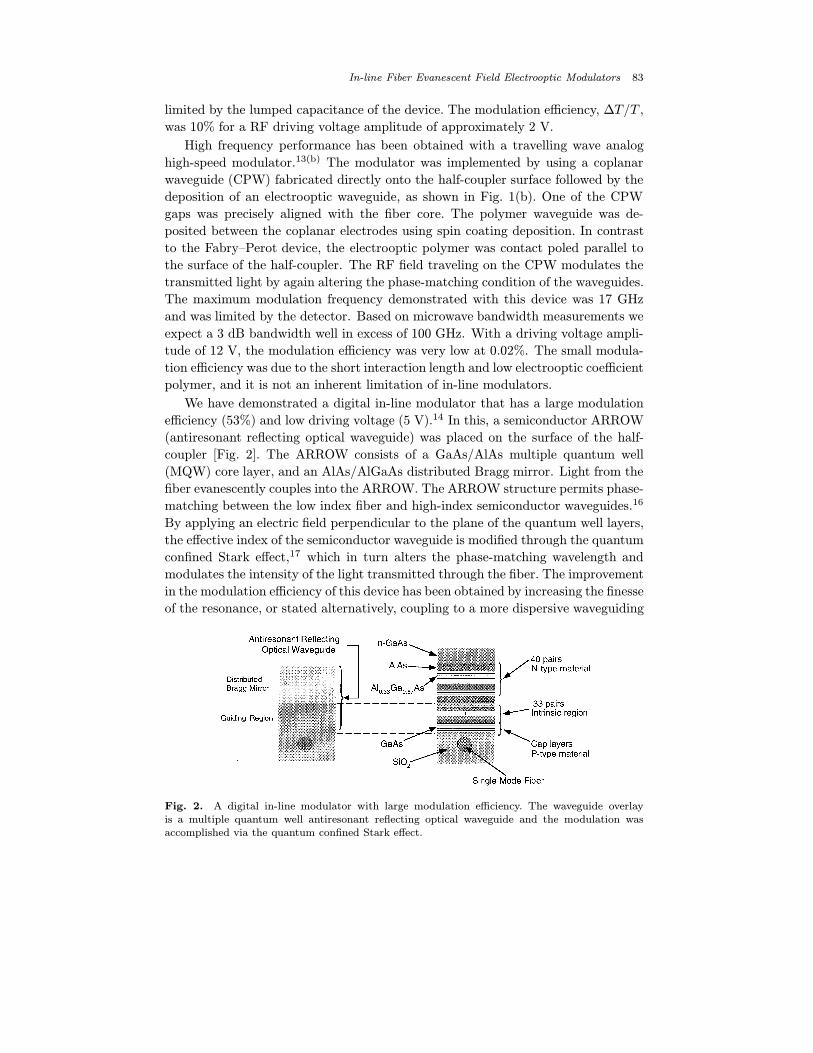
We have demonstrated a digital in-line modulator that has a large modulation
efficiency (53%) and low driving voltage (5 V).14 In this, a semiconductor ARROW
(antiresonant reflecting optical waveguide) was placed on the surface of the half-
coupler [Fig. 2]. The ARROW consists of a GaAs/AlAs multiple quantum well
(MQW) core layer, and an AlAs/AlGaAs distributed Bragg mirror. Light from the
fiber evanescently couples into the ARROW. The ARROW structure permits phase-
matching between the low index fiber and high-index semiconductor waveguides.16
By applying an electric field perpendicular to the plane of the quantum well layers,
the effective index of the semiconductor waveguide is modified through the quantum
confined Stark effect,17 which in turn alters the phase-matching wavelength and
modulates the intensity of the light transmitted through the fiber. The improvement
in the modulation efficiency of this device has been obtained by increasing the finesse
of the resonance, or stated alternatively, coupling to a more dispersive waveguiding
Fig. 2. A digital in-line modulator with large modulation efficiency. The waveguide overlayis a multiple quantum well antiresonant reflecting optical waveguide and the modulation wasaccomplished via the quantum confined Stark effect.
84 C. Arft et al.
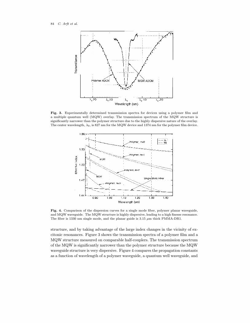
Fig. 3. Experimentally determined transmission spectra for devices using a polymer film anda multiple quantum well (MQW) overlay. The transmission spectrum of the MQW structure issignificantly narrower than the polymer structure due to the highly dispersive nature of the overlay.The center wavelength, λ0, is 827 nm for the MQW device and 1374 nm for the polymer film device.
Fig. 4. Comparison of the dispersion curves for a single mode fiber, polymer planar waveguide,and MQW waveguide. The MQW structure is highly dispersive, leading to a high finesse resonance.The fiber is 1330 nm single mode, and the planar guide is 3.15 µm thick PMMA-DR1.
structure, and by taking advantage of the large index changes in the vicinity of ex-
citonic resonances. Figure 3 shows the transmission spectra of a polymer film and a
MQW structure measured on comparable half-couplers. The transmission spectrum
of the MQW is significantly narrower than the polymer structure because the MQW
waveguide structure is very dispersive. Figure 4 compares the propagation constants
as a function of wavelength of a polymer waveguide, a quantum well waveguide, and
In-line Fiber Evanescent Field Electrooptic Modulators 85
an optical fiber. The effective indices for the fiber and the slab were calculated using
their respective eigenvalue equations. The propagation constants of the quantum
well waveguide were calculated using the transfer-matrix approach18 and the com-
plex refractive indices of the AlxGa1−xAs layers.19 The figure indicates that the
propagation constant of a mode in the ARROW has a very large dispersion, leading
to a resonance with a large finesse, which results in a large modulation. This MQW
device illustrates that an in-line modulator can obtain large modulation efficiencies
even though the wavelength of operation is close to an absorption maximum. Unlike
other guided wave modulators, in an in-line evanescent modulator the interaction
with the electrooptic region is only where the modulation takes place and therefore
advantage can be taken of the resonant enhancement of nonlinearities in the vicinity
of material absorptions.
3. Modeling of In-line Fiber Half-Coupler Devices
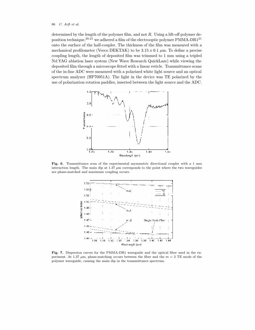
A schematic model of an in-line fiber evanescent modulator is shown in Fig. 5. The
cladding of the fiber is assumed to be infinite below the boundary between the slab
and cladding. This is a valid approximation because the fiber mode field is essentially
zero at the cladding boundary. The more complex electromagnetic interactions in
the ADCM, in comparison to conventional couplers, make the modeling of these
devices more challenging. In this paper we report the results of an experiment in
which the material and device parameters are well known, and discuss the ability
of simulation methods to reproduce the measured results.
For the experiment we used a half-coupler that consists of a side-polished
1330 nm single mode optical fiber affixed in a segmented silicon v-groove. This
particular half-coupler has a very large radius of curvature, R, of 1200 cm, see
Fig. 5. When a polymer film is placed on the side-polished fiber, the large radius of
curvature of the v-groove half-coupler ensures that the interaction length is mainly
Fig. 5. Schematic of the asymmetric directional coupler model. Lslab = 1 mm, tslab = 3.15 µm,ncover = 1, R = 12 m, a = 4.15 µm, nfiber = ncladding + ∆f , where ∆f = 0.0045. Sellmeierequations for glass and PMMA-DR1 describe the indices ncladding and nslab, respectively. Thepolishing depth, s0, is used as a fitting parameter for the simulation.
86 C. Arft et al.
determined by the length of the polymer film, and not R. Using a lift-off polymer de-
position technique,20,21 we adhered a film of the electrooptic polymer PMMA-DR121
onto the surface of the half-coupler. The thickness of the film was measured with a
mechanical profilometer (Veeco DEKTAK) to be 3.15± 0.1 µm. To define a precise
coupling length, the length of deposited film was trimmed to 1 mm using a tripled
Nd:YAG ablation laser system (New Wave Research QuickLaze) while viewing the
deposited film through a microscope fitted with a linear reticle. Transmittance scans
of the in-line ADC were measured with a polarized white light source and an optical
spectrum analyzer (HP70951A). The light in the device was TE polarized by the
use of polarization rotation paddles, inserted between the light source and the ADC.
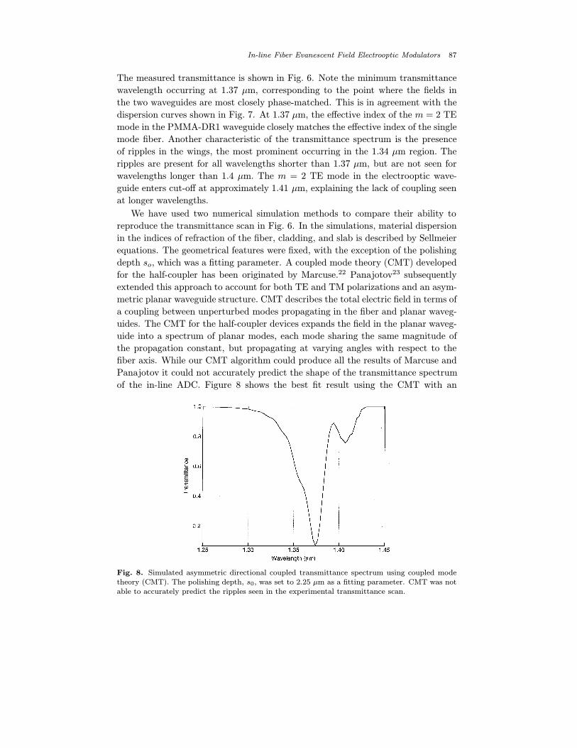
Fig. 6. Transmittance scan of the experimental asymmetric directional coupler with a 1 mminteraction length. The main dip at 1.37 µm corresponds to the point where the two waveguidesare phase-matched and maximum coupling occurs.
Fig. 7. Dispersion curves for the PMMA-DR1 waveguide and the optical fiber used in the ex-periment. At 1.37 µm, phase-matching occurs between the fiber and the m = 2 TE mode of thepolymer waveguide, causing the main dip in the transmittance spectrum.
In-line Fiber Evanescent Field Electrooptic Modulators 87
The measured transmittance is shown in Fig. 6. Note the minimum transmittance
wavelength occurring at 1.37 µm, corresponding to the point where the fields in
the two waveguides are most closely phase-matched. This is in agreement with the
dispersion curves shown in Fig. 7. At 1.37 µm, the effective index of the m = 2 TE
mode in the PMMA-DR1 waveguide closely matches the effective index of the single
mode fiber. Another characteristic of the transmittance spectrum is the presence
of ripples in the wings, the most prominent occurring in the 1.34 µm region. The
ripples are present for all wavelengths shorter than 1.37 µm, but are not seen for
wavelengths longer than 1.4 µm. The m = 2 TE mode in the electrooptic wave-
guide enters cut-off at approximately 1.41 µm, explaining the lack of coupling seen
at longer wavelengths.
We have used two numerical simulation methods to compare their ability to
reproduce the transmittance scan in Fig. 6. In the simulations, material dispersion
in the indices of refraction of the fiber, cladding, and slab is described by Sellmeier
equations. The geometrical features were fixed, with the exception of the polishing
depth so, which was a fitting parameter. A coupled mode theory (CMT) developed
for the half-coupler has been originated by Marcuse.22 Panajotov23 subsequently
extended this approach to account for both TE and TM polarizations and an asym-
metric planar waveguide structure. CMT describes the total electric field in terms of
a coupling between unperturbed modes propagating in the fiber and planar waveg-
uides. The CMT for the half-coupler devices expands the field in the planar waveg-
uide into a spectrum of planar modes, each mode sharing the same magnitude of
the propagation constant, but propagating at varying angles with respect to the
fiber axis. While our CMT algorithm could produce all the results of Marcuse and
Panajotov it could not accurately predict the shape of the transmittance spectrum
of the in-line ADC. Figure 8 shows the best fit result using the CMT with an
Fig. 8. Simulated asymmetric directional coupled transmittance spectrum using coupled modetheory (CMT). The polishing depth, s0, was set to 2.25 µm as a fitting parameter. CMT was notable to accurately predict the ripples seen in the experimental transmittance scan.
88 C. Arft et al.
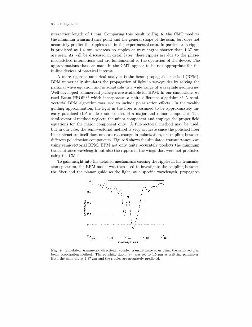
interaction length of 1 mm. Comparing this result to Fig. 6, the CMT predicts
the minimum transmittance point and the general shape of the scan, but does not
accurately predict the ripples seen in the experimental scan. In particular, a ripple
is predicted at 1.4 µm, whereas no ripples at wavelengths shorter than 1.37 µm
are seen. As will be discussed in detail later, these ripples are due to the phase-
mismatched interactions and are fundamental to the operation of the device. The
approximations that are made in the CMT appear to be not appropriate for the
in-line devices of practical interest.
A more rigorous numerical analysis is the beam propagation method (BPM).
BPM numerically simulates the propagation of light in waveguides by solving the
paraxial wave equation and is adaptable to a wide range of waveguide geometries.
Well-developed commercial packages are available for BPM. In our simulations we
used Beam PROP,24 which incorporates a finite difference algorithm.25 A semi-
vectorial BPM algorithm was used to include polarization effects. In the weakly
guiding approximation, the light in the fiber is assumed to be approximately lin-
early polarized (LP modes) and consist of a major and minor component. The
semi-vectorial method neglects the minor component and employs the proper field
equations for the major component only. A full-vectorial method may be used,
but in our case, the semi-vectorial method is very accurate since the polished fiber
block structure itself does not cause a change in polarization, or coupling between
different polarization components. Figure 9 shows the simulated transmittance scan
using semi-vectorial BPM. BPM not only quite accurately predicts the minimum
transmittance wavelength but also the ripples in the wings that were not predicted
using the CMT.
To gain insight into the detailed mechanisms causing the ripples in the transmis-
sion spectrum, the BPM model was then used to investigate the coupling between
the fiber and the planar guide as the light, at a specific wavelength, propagates
Fig. 9. Simulated asymmetric directional coupler transmittance scan using the semi-vectorialbeam propagation method. The polishing depth, s0, was set to 1.5 µm as a fitting parameter.Both the main dip at 1.37 µm and the ripples are accurately predicted.
In-line Fiber Evanescent Field Electrooptic Modulators 89
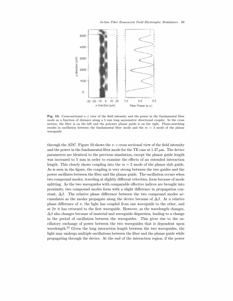
Fig. 10. Cross-sectional x–z view of the field intensity and the power in the fundamental fibermode as a function of distance along a 5 mm long asymmetric directional coupler. In the crosssection, the fiber is on the left and the polymer planar guide is on the right. Phase-matchingresults in oscillation between the fundamental fiber mode and the m = 2 mode of the planarwaveguide.
through the ADC. Figure 10 shows the x–z cross sectional view of the field intensity
and the power in the fundamental fiber mode for the TE case at 1.37µm. The device
parameters are identical to the previous simulation, except the planar guide length
was increased to 5 mm in order to examine the effects of an extended interaction
length. This clearly shows coupling into the m = 2 mode of the planar slab guide.
As is seen in the figure, the coupling is very strong between the two guides and the
power oscillates between the fiber and the planar guide. The oscillation occurs when
two compound modes, traveling at slightly different velocities, form because of mode
splitting. As the two waveguides with comparable effective indices are brought into
proximity, two compound modes form with a slight difference in propagation con-
stant, ∆β. The relative phase difference between the two compound modes ac-
cumulates as the modes propagate along the device because of ∆β. At a relative
phase difference of π, the light has coupled from one waveguide to the other, and
at 2π it has returned to the first waveguide. However, as the wavelength changes,
∆β also changes because of material and waveguide dispersion, leading to a change
in the period of oscillation between the waveguides. This gives rise to the os-
cillatory exchange of power between the two waveguides that is dependent upon
wavelength.22 Given the long interaction length between the two waveguides, the
light may undergo multiple oscillations between the fiber and the planar guide while
propagating through the device. At the end of the interaction region, if the power
90 C. Arft et al.
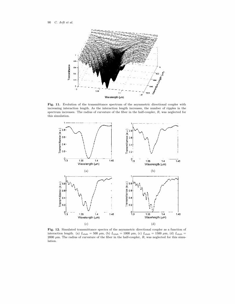
Fig. 11. Evolution of the transmittance spectrum of the asymmetric directional coupler withincreasing interaction length. As the interaction length increases, the number of ripples in thespectrum increases. The radius of curvature of the fiber in the half-coupler, R, was neglected forthis simulation.
(a) (b)
(c) (d)
Fig. 12. Simulated transmittance spectra of the asymmetric directional coupler as a function ofinteraction length. (a) Lslab = 500 µm, (b) Lslab = 1000 µm, (c) Lslab = 1500 µm, (d) Lslab =2000 µm. The radius of curvature of the fiber in the half-coupler, R, was neglected for this simu-lation.
In-line Fiber Evanescent Field Electrooptic Modulators 91
is predominantly in the fiber, a peak in the transmission spectrum will occur, while
if it is in the planar guide, a valley will occur. The amplitude of the oscillation
changes with distance, which is indicative of more complicated behavior compared
to a symmetric coupler.
The transmittance was then calculated as a function of wavelength and inter-
action length to investigate further the wavelength dependent oscillation of power
between the two waveguides. Figure 11 shows the simulated transmittance spectrum
for an ADC as a function of interaction length. Figures 12(a)–(d) show the same
transmittance spectrum but plotted at interaction lengths corresponding to 500 µm,
1000 µm, 1500 µm, and 2000 µm. The device model used is identical to the previous
model but neglects the radius of curvature of the fiber, R. For short interaction
lengths, very few ripples are seen, but as the interaction length increases, more
ripples appear in the transmittance. This simply occurs because as the interaction
length is increased, the two compound modes of the ADC accumulate more relative
phase difference between them. Therefore, it requires less of a change of ∆β, i.e. less
of a change in wavelength, to cause the two compound modes to oscillate in and
out of phase, leading to a larger number of ripples in the transmittance spectrum
with increasing interaction length.
Previous CMT simulation results22 predict that, depending upon the relative
index difference between the fiber and slab, the light coupled into the slab may be
lost into a continuum of slab modes, oscillate between the guides because of beating
of two compound modes, or settle into a guided mode, with the slab and fiber
acting as a ridge waveguide. An example was given showing that when the index of
refraction of the planar guide was much larger than the index of the fiber, the
light in the fiber exponentially decayed as the power was transferred into the slab
modes, which were unguided in the lateral dimension. If this is a general rule, the
implication for in-line modulators will be that the modulation efficiency will scale
poorly with interaction length. In this paper we show the power in the fiber does
not always decay exponentially, and that confined modes may exist in the planar
waveguide, despite the fact that the index of the polymer (approximately 1.54)
is considerably higher than the index of the optical fiber (approximately 1.45).
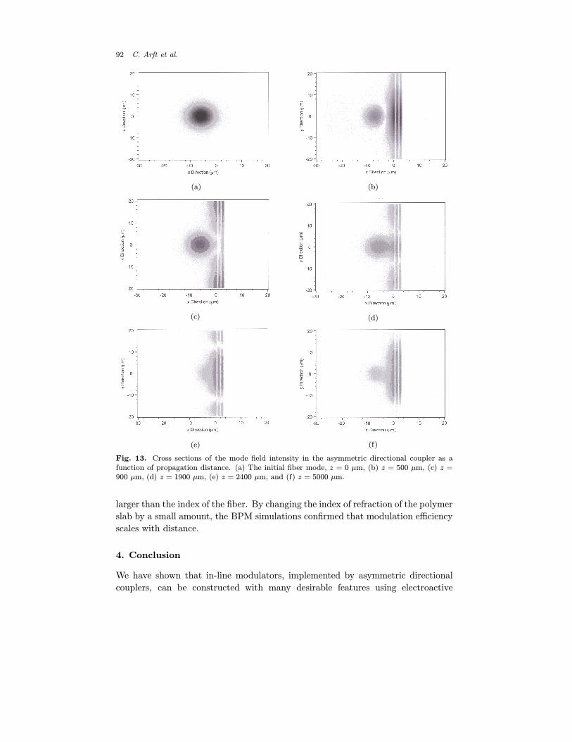
Figure 13 shows x–y cross sections of the propagating mode as a function of distance
along the device. The initial fiber mode is shown in Fig. 13(a). Figure 13(b) shows
the mode at z = 500 µm, corresponding to the first point where the light has
coupled predominantly to the slab (see also Fig. 10). While some of the light is
spreading out along the slab, much of it remains confined in close proximity to the
fiber in a compound fiber-slab mode, transferring power between the waveguides.
In Fig. 13(c), the light propagating in the oscillating compound mode has coupled
back into the fiber. Figure 13(d) shows a point of maximum coupling to the fiber
at z = 1900 µm. The light is maximally coupled to the slab in Fig. 13(e) at z =
2400 µm. Even as the end of the slab is reached [Fig. 13(f)], we see that much of
the power is still confined in close proximity to the fiber. These guided, compound
fiber-slab modes exist, even though the index of refraction of the planar guide is
92 C. Arft et al.
(a) (b)
(c) (d)
(e) (f)
Fig. 13. Cross sections of the mode field intensity in the asymmetric directional coupler as afunction of propagation distance. (a) The initial fiber mode, z = 0 µm, (b) z = 500 µm, (c) z =900 µm, (d) z = 1900 µm, (e) z = 2400 µm, and (f) z = 5000 µm.
larger than the index of the fiber. By changing the index of refraction of the polymer
slab by a small amount, the BPM simulations confirmed that modulation efficiency
scales with distance.
4. Conclusion
We have shown that in-line modulators, implemented by asymmetric directional
couplers, can be constructed with many desirable features using electroactive
In-line Fiber Evanescent Field Electrooptic Modulators 93
polymers and multiple quantum well compound semiconductors. All in-line modu-
lators to date have used half-couplers that severely limited the interaction with the
electrooptic region. Unlike the compound semiconductor devices, which have large
modulation efficiencies even at short interaction lengths, the polymer modulators
have low modulation efficiency and increasing the optical interaction region will be
desirable. Based on a comparison between experimental and theoretical results, it
was shown that BPM can simulate the in-line electrooptic polymer modulators. It
was further shown that compound modes exist in this structure that propagate
over large distances, which could lead to an increase in modulation efficiency with
distance. The large radius of curvature of the v-groove half-coupler does allow very
long interaction length in-line fiber devices. The results from this BPM simulation
encourage further study of long interaction length ADC devices and the gains in
modulation efficiency that can be achieved.
Acknowledgments
We gratefully acknowledge Professor Shiao-Ming Tsen, National Tsin Hua Univer-
sity, Taiwan, for the silicon v-groove half-couplers. Most of this work was supported
by the Office of the Secretary of Defense through MURI program grant number
N00014-97-1-1006. We also acknowledge the partial support of this work by the
CPIMA MRSEC Program of the National Science Foundation under award num-
ber DMR-9808677 for CPIMA II. Stanford University acknowledges support from
DARPA/ONR through contract number N00014-98-1-0537.
References
1. N. Dagli, IEEE Trans. Microwave Theory Tech. 47, 1151 (1999).2. K. Noguchi, H. Miyazawa and O. Mitomi, Electron. Lett. 30, 949 (1994).3. G. K. Gopalakrishnan, W. K. Burns and C. H. Bulmer, Electron. Lett. 28, 207 (1992).4. (a) D. G. Girton, S. L. Kwiatkowski, G. F. Lipscomb and R. S. Lytel, Appl. Phys.
Lett. 58, 1730 (1991). (b) C. C. Teng, Appl. Phys. Lett. 60, 1538 (1992). (c) D. Chen,H. R. Fetterman, A. Chen, W. H. Steier, L. R. Dalton, W. Wang and Y. Shi, Appl.Phys. Lett. 70, 3335 (1997).
5. S. A. Hamilton, D. R. Yankelevich, A. Knoesen, R. T. Weverka and R. A. Hill, IEEETrans. Microwave Theory Tech. 47, 1184 (1999).
6. E. Ackerman, S. Wanuga, D. Kasemset, A. S. Daryoush and N. R. Samant, IEEETrans. Microwave Theory Tech. 41, 1299 (1993).
7. SFDR for HP8349B wideband amplifier based on 15 dB power gain, −174 dBm/Hzinput thermal noise power and 13 dB noise figure and 1 MHz bandwidth.
8. M. L. Farwell, W. S. C. Chang and D. R. Huber, IEEE Photon. Tech. Lett. 5, 779(1993).
9. R. A. Bergh, G. Kotler and H. J. Shaw, Electron. Lett. 16, 260 (1980).10. Canadian Instrumentation and Research Ltd., Toronto, Canada.11. S. Creaney, W. Johnstone and K. McCallion, IEEE Photon. Tech. Lett. 8, 355 (1996).12. F. Pan, K. McCallion and M. Chiappetta, Appl. Phys. Lett. 74, 492 (1999).13. (a) R. A. Hill, G. C. Bjorklund, S. A. Hamilton, D. R. Yankelevich and A. Knoe-
sen, Low-distortion, high-speed polymeric in-line fiber modulator — CLEO ‘96, (1996),p. 332. (b) S. A. Hamilton, D. R. Yankelevich, A. Knoesen, R. T. Weverka, R. A. Hill
94 C. Arft et al.
and G. C. Bjorklund, J. Opt. Soc. Am. B15, 740 (1998). (c) S. A. Hamilton, D. R.Yankelevich, A. Knoesen, R. A. Hill, R. T. Weverka and G. C. Bjorklund, IEEE Lasersand Electrooptics Society, Vol. 1 of 1997 IEEE Technical Digest Series, Institute ofElectrical and Electronics Engineers, Piscataway, NJ (1997) p. 387.
14. E. Mao, C. W. Coldren, J. S. Harris, D. Yankelevich, O. Solgaard and A. Knoesen,Appl. Phys. Lett. 75, 310 (1999).
15. Half-couplers have been acquired from Canadian Instrumentation and Research Ltd.,Toronto, Canada.
16. B. Pezeshki, F. Agahi and J. A. Kash, Appl. Phys. Lett. 69, 2807 (1996).17. D. A. B. Miller, D. S. Chemla, T. C. Damen, A. C. Gossard, W. W. Wiegmann,
T. H. Wood and C. A. Burrus, Phys. Rev. B32, 1043 (1985).18. A. Ghatak, K. Thyagarajan and M. R. Shnoy, J. Lightwave Tech. 5, 660 (1987).19. S. Adachi, J. Appl. Phys. 58, R1 (1985).20. G. Khanarian, M. A. Mortazavi and A. J. East, Appl. Phys. Lett. 63, 1462 (1993).21. Ph. Pretre, L.-M. Wu, R. A. Hill and A. Knoesen, J. Opt. Soc. Am. B15, 379 (1998).22. D. Marcuse, J. Lightwave Tech. 7, 122 (1989).23. K. Panajotov, J. Lightwave Tech. 12, 983 (1994).24. Rsoft, Inc., 200 Executive Blvd. Ossining, NY 10562.25. R. Scarmozzino and R. M. Osgood, Jr., J. Opt. Soc. Am. A8, 724 (1991).