in-situ diagnostics and prognostics of wire bonding … pe-condition... · analytical and...
TRANSCRIPT

1
Bing Ji, Member, IEEE, Volker Pickert, Member, IEEE,
Wenping Cao, Senior Member, IEEE, Bashar Zahawi, Senior Member, IEEE
Corresponding author:
Dr Wenping Cao
E3.18 Merz Court
Power Electronics, Drives and Machines Group
School of Electrical & Electronic Engineering
Newcastle University upon Tyne
NE1 7RU UK
Tel: +44 (0)191 2227326
Fax: +44 (0)191 2228180
Email: [email protected]
The paper has not been presented at a conference or submitted elsewhere previously.
Abstract—This paper presents a diagnostic and prognostic condition monitoring method for IGBT power modules for use primarily in
electric vehicle applications. The wire bond related failure, one of the most commonly observed packaging failures, is investigated by
analytical and experimental methods using the on-state voltage drop as a failure indictor. A sophisticated test bench is developed to generate
and apply the required current/power pulses to the device under test. The proposed method is capable of detecting small changes in the failure
indicators of the IGBTs and freewheeling diodes (FWDs) and its effectiveness is validated experimentally. The novelty of the work lies in the
accurate online testing capacity for diagnostics and prognostics of the power module with a focus on the wire bonding faults, by injecting
external currents into the power unit during the idle time. Test results show the IGBT may sustain a loss of half the bond wires before the
In-Situ Diagnostics and Prognostics of Wire
Bonding Faults in IGBT Modules for
Electric Vehicle Drives

2
impending fault becomes catastrophic. The measurement circuitry can be embedded in the IGBT drive circuits and the measurements can be
performed in-situ when the electric vehicle stops in stop-and-go, red light traffic conditions or during routine servicing.
Index Terms—Electric vehicles, heating, insulated gate bipolar transistors, monitoring, power electronics, reliability testing.
I. INTRODUCTION
VER the last 20 years, electric vehicle (EV) technologies have taken a significant leap forward, primarily aided by advances in
electrical motor drives, power converters, batteries and system configuration. Generally, EVs can be classifies as hybrid electric
vehicles (HEVs), plug-in hybrid electric vehicles (PHEVs), more electric vehicles (MEVs) and all electric vehicles (AEVs), depending
on the electrification level of the vehicles. EVs represent a cost-sensitive market and new technologies are under development to
improve their system performance while driving down the cost. In addition to initial costs, the reliability of key components is an
important performance indicator which affects operational costs and could make the difference between success and failure of a concept
in the marketplace.
Power electronic converters are widely used in electric traction drive applications [1]-[9] while multi-chip insulated-gate bipolar
transistor (IGBT) power modules are the most commonly used power switches for the EVs’ on-board power converters [10][11].
However, IGBTs are known to be prone to failure [12]-[19], and the situation would only get worse when operating in the harsh
environment beneath the bonnet of an electric vehicle. Table I presents typical environmental conditions and operational requirements
for automotive applications [13][20]. Clearly, the performance and reliability of IGBT modules are constrained by these stringent
conditions which lead to exposure to high temperatures, high levels of humidity, extreme cyclic loading and mechanical stress [21]-[25].
Among these, thermo-mechanical stress is an overriding factor that causes IGBT packaging connector fatigue [12][26]-[30] (such as
bond wire and solder connection failures). Because of improved solder technologies [31]-[32], wirebonds are generally observed as the
major type of packaging failures to reduce the lifetime of IGBTs [19][33]-[35] and thus are the focus of this paper.
O

3
TABLE I
ENVIRONMENTAL CONDITIONS AND OPERATIONAL REQUIREMENTS
Parameter Value
Ambient air temperature -40˚C to 135˚C
Coolant water temperature -40˚C to 105˚C
Junction temperature -40˚C to 175˚C
Temperature cycling 1000 cycles @ ∆T=165˚C
Power cycling 30,000 cycles @∆T=100˚C
Humidity 85%
Vibration 10 g
Shock 50 g
Operational life 131,400 h
At present, wire bonding is the dominant technology used to connect the terminals (or leads) to the semiconductor chips because this
is still a straightforward, flexible and cost-effective solution. Recent advances in new composition wire materials [36] and new bonding
technologies (e.g. special coating and strain buffer bonding [12]) have received much attention by the industry. Nonetheless, when the
bonding using these new technologies fails, the entire device will be damaged with catastrophic consequences.
Without a doubt, the detection of an IGBT fault prior to (prognosis) or even after (diagnosis) its occurrence is of critical importance to
the healthy operation of the system. Conventional vehicles are equipped with an on-board diagnostic (OBD) system which can detect a
“happened” fault and flag it up to the driver of the vehicle. In the event of an IGBT failure, the detection must be quick enough (ideally,
less than 10 μs) to prevent a fault from propagating, which places a limit on the hardware setup [37]-[40]. Obviously, there is an
increasing need for prognostic detection technologies to provide state-of-health or early warning information. Traditional reliability
prediction methods include Mil-HDBK-217, 217-PLUS, PRISM, Telcordia and FIDES. These are empirical methods based on
statistical data and average performance of a large number of identical products. In essence, they account little for the mechanisms of
complex in-service failures. It is thus not surprising that the results obtained from these methods do not always correlate well with actual
failures in the field [41].
Recently, some advanced prognostic techniques have been proposed to predict semiconductor devices’ impending failures. First, a
range of detecting elements may be embedded within the host device and their failures provide an early warning signal. This is called the
Canary method [42]. The second method is the analytical lifetime prediction based on Coffin-Manson models [43][44],
Norris-Landzberg models [45][46], or Bayerer’s models [47]. The lifetime expectancy (in numbers of cycles) of an IGBT is
4
experimentally obtained from new at given environmental and load conditions. The cumulative fatigue (or damage) of an IGBT is
calculated based on actual operational conditions and its remaining useful life (RUL) is then expressed as the number of cycles to
failures [25][48][49]. The third method is the failure precursor method. This is realized by observing changes in either fault-related
parameters [28] or by adding purpose-built embedded sensors [50][51]. All these methods have advantages and drawbacks. The first
method is technically effective but provides limited information of device life consumption. It is irreversible and also affects the system
architecture of the chip. The second can offer quantitative information of the RUL from exhaustive tests but the parameters associated
with different stress conditions are not fully considered. For instance, humidity and mechanical stress are key parameters but are not
accounted for. The third method is indirect and easy to implement while the complex relationship between failures and precursors is
over simplified. Overall, failure mechanisms have not been fully understood and these methods cannot be applied in service conditions.
This work evolves from the third method and extends it to in-situ condition monitoring (CM) of IGBTs and free-wheeling diodes
(FWDs). The monitoring circuitry can be embedded in an advanced gate drive unit (GDU) while the diagnostic and prognostic tests can
be conducted during stop-and-go traffic conditions or routine services.
The paper is organized as follows. Wire bond failure mechanisms and their prognostic parameters are explained in Section II. An
on-board condition monitoring system is presented for practical applications in Section III. The analytical and experimental work is
described and discussed in Section IV, followed by the conclusions in Section V.
II. FAILURE MECHANISMS AND PROGNOSTIC PARAMETERS
All conventional power modules have a structure of multiple layers. The schematic cross-section of a wire-bonded IGBT module is
shown in Fig. 1. When viewed from the top, the aluminum wire is bonded to the chip top metallization to connect the semiconductor
chips, as in the case of IGBTs and FWDs. The silicon chips are soldered onto a metal plated ceramic substrate, which is soldered onto
the baseplate. The IGBT module is encapsulated with silicone gel to increase its physical integrity.

5
Silicone gel
Semiconductor
chipBond wire
Cover
Terminal
Isolation substrate with copper
foils on both sides
Base plate
(Copper)
Fig.1 Schematic cross-section of the IGBT power module.
A. Failure mechanisms of wire bonds
During normal operation of IGBTs, semiconductor chips will generate heat and pass it by conduction onto the heat sink through
layers of components, leading to a temperature gradient within the multilayer structure and thus a thermo-mechanical stress. Similarly,
as the ambient or junction temperature varies, a thermo-mechanical stress is also created on layer interfaces as well as within each layer.
These can be explained by thermal expansion as in Eq (1),
TCTEl
l
(1)
where l and ∆l are the length and its deviation subject to a temperature gradient ∆T, and CTE stands for the coefficient of thermal
expansion.
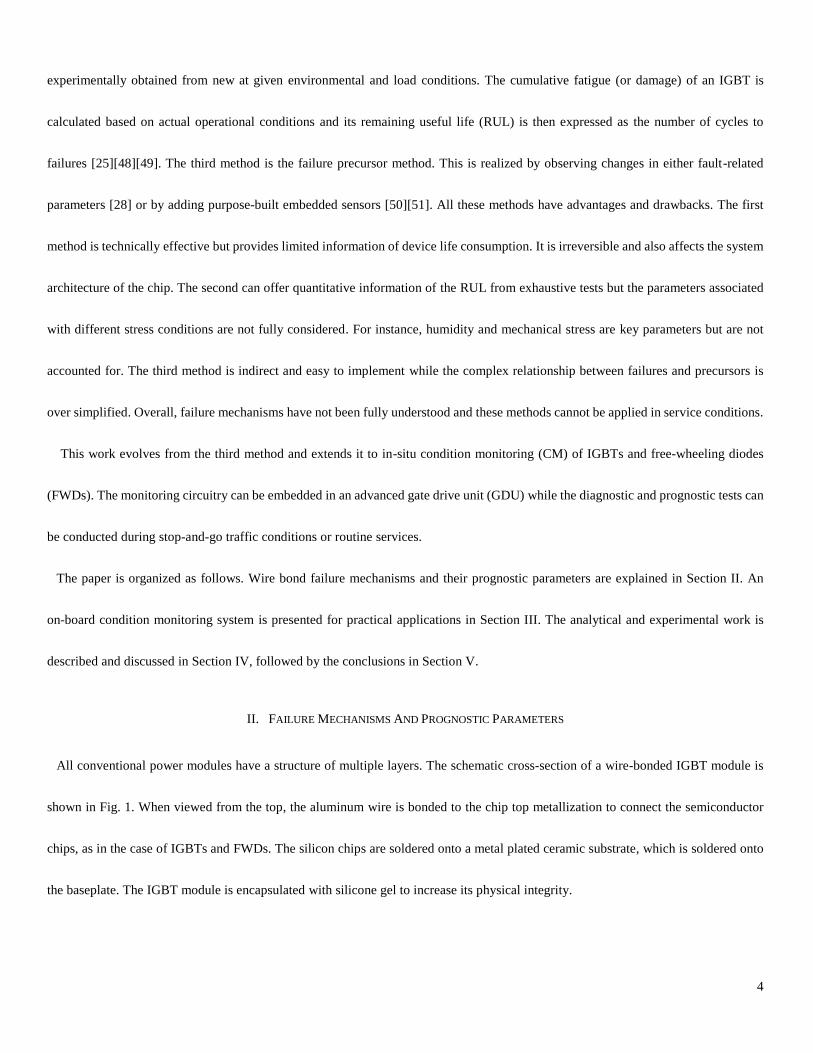
Table II gives the CTE values for common materials used in IGBTs. Because the layers of IGBTs are made of materials with different
CTEs, a physical departure or crack may be created after undergoing repetitive thermal cycling, power cycling or mechanical stress
during operation. This is particularly pertinent for electric vehicle applications [13][20] because the operation of vehicles involves
frequent acceleration, regenerative braking and cruising. Among major causes, the repetitive temperature swing account for the majority
of long-term packaging-related wear-out failures. For every 10ºC increase in the operating environment, the failure rate is doubled [52].
Typical junction temperature swings resulting from both device self-heating and environmental temperature variations are illustrated in
Fig. 2.
6
TABLE II
CTES OF COMMON ELECTRONIC MATERIALS
Part Material CTE (ppm/ºC)
Silicone gel Silicone resin 30-300
Terminal Copper 17.5
Ni plating Nickel 13.4
Solder layer Solder 15-30
Bond wire Aluminum 22.5
Chip metallization Aluminum 22.5
Chip Silicon 4.1
Isolation substrate Aluminum oxide 8.3
Aluminum nitride 5.7
Baseplate Copper 17.5
Aluminum silicon carbide 5-15
160
140
120
100
80
60
40
20
0
Time (mins)
Tem
pera
ture
(°C
)
∆Theat sink
∆Tj
heat sink
temperature
junction
temperature
0 1 2 3 4 5
Fig. 2 Typical junction temperature swings of a power device.
In general, the wire bonding faults of IGBTs are caused by bonding wire lift-off, heel cracking or aluminum metallization
reconstruction. Fig. 3 shows the images of these three damage accumulations at bonded interfaces. The damage generally starts from a
tiny crack and can propagate over time to result in an open-circuit or a short-circuit failure. Furthermore, the deformation of bond wires
and their length variations will also escalate the damage. IGBT modules always use multiple wires bonded in parallel to increase their
current-carrying capability. If a bond wire is open-circuited due to a fault, current loading passing through other wires is increased and
so is their temperature (self-heating). As a consequence, the aging process of IGBTs will be accelerated. The same is true for chip
metallization reconstruction as it increases the contact resistance and joule loss. Obviously, all these adverse effects raise the
temperature which may lead to the melting of the metal joints if left untreated. Moreover, the increased heat is also likely to pass through
the silicon chip causing severe damages or malfunctions such as latch-up [12][18], hot-spots [12] or even burn-outs.

7
(a) Bond wire lift-off (b) Heel cracking
(c) Chip metallization reconstruction
Fig. 3 Photographs of three types of wire bonding faults [30].
B. Prognostic parameters for detecting bond wire degradation
IGBTs’ bond wire fatigue and chip metallization reconstruction can be directly evaluated by measuring their shear stress or crack
length. This normally calls for special equipment and is only implemented as offline measurements [53]. Since the IGBTs’ aging
process leads to progressive changes in their internal resistance and terminal voltage drop during forward conduction (VCE(on) for IGBTs
and VF(on) for FWDs), the two parameters can be used as prognostic health indicators to establish a correlation between ageing and
impending failures of the devices [14][54].
Fig. 4 shows a photograph and the static equivalent circuit of a 70A half-bridge IGBT module SKM 50GB063D used in this work. In
this figure, the device terminal voltage drop (VT) is given by the sum of the voltage drop across the silicon chip (Vchip) and the voltage
drop across the stray resistance (Vstray). In principle, Vchip varies with the junction temperature and load current. For IGBTs, it is also
affected by the gate-emitter voltage. Also in the figure, the stray resistance is comprised of five parts: 1) the effective resistance across
Healthy Faulty

8
the bond wire and bonding interface (REE’1, RAA’1, REE’2 and RAA’2); 2) the contact resistance of the chip metallization pad (RME’1, RMA’1,
RME’2 and RMA’2); 3) the resistance of the die attachment (RCC’1, RKK’1, RCC’2 and RKK’2); 4) the resistance of directly bonded copper layer
(RCu); and 5) the resistance of the terminal and its contact (RL1, RL2 and RL3).
L1 RCu
RL3RG1
L3
RE1RC1
RKK’1
RCC’1
RMA1
RME1
Vchip
VT
RAA’1
REE’1
RG2
RKK’2
RCC’2
RMA2
RME2
RAA’2
REE’2
RL1
RC2
L2RCuRL2RL12RCu RCu
RCu
RE2
VT
Vchip
Fig. 4 Photograph and static equivalent circuit of a half-bridge IGBT module.
In addition to self-heating, parts 1-3 of the stray resistance would also experience substantial temperature swings arising from the
operation of semiconductor chips they are directly connected to. Changes in parts 1-3 are key to the indication of the state of health of
the IGBT and should be detected for prognostic purposes. Although parts 4 and 5 are not in the proximity of the chip (thus less likely to
be affected by the chip’s thermal cycles), they can still be affected by the degradation of the terminal lead joints which raises the contact
resistance of the terminal joints, and in turn, increases the forward voltage drop [55]. For this reason, the IGBT’s on-state voltage in this
paper is measured between the collector power terminal and the Kelvin emitter terminal, rather than the voltage between the collector
and emitter of the power terminals.
(1) (2) (3) (4) (5)
For measurement For measurement Kelvin emitter Kelvin emitter

9
III. PROPOSED DIAGNOSTIC AND PROGNOSTIC METHOD AND EXPERIMENTAL SETUP
As explained previously, existing diagnostic and prognostic methods are limited. One of the clear technical challenges is the
extraction of small signals (mV) from larger ones (hundreds of volts) meaning that conventional methods can not apply to in-situ
measurements. That is, the variations in prognostic parameters resulting from ageing are relatively small so that measured signals can be
overwhelmed by noise or disturbances in the EV power network which are associated with changes in operating conditions
(temperature, loading or control). As a result, much effort in this work is directed at improving the measurement accuracy.
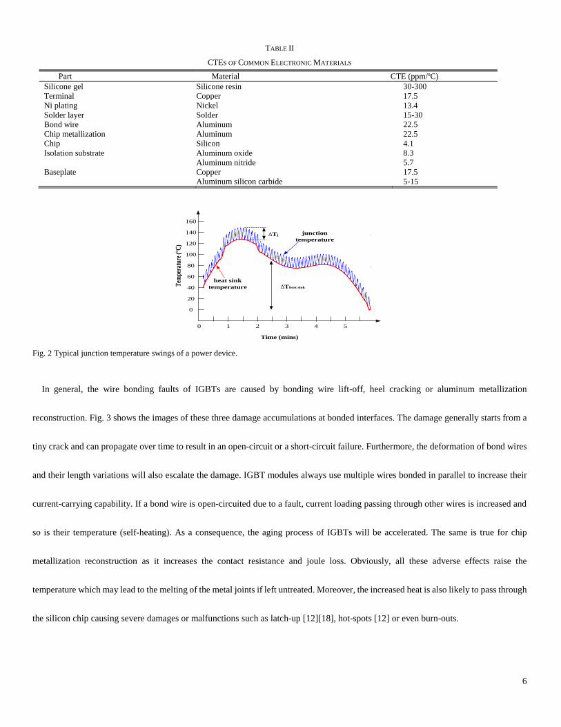
Fig. 5 shows photographs and schematic diagrams of the complete experimental setup. In Fig. 5(a), the DUTs (IGBTs) are placed in
the thermal chamber to maintain a required testing environment and tested using the proposed on-board CM circuit. In Fig. 5(b), T1-T6
are six identical IGBTs, D1-D6 are six FWDs and M is an electric motor. The measurement circuitry consists of: 1) an auxiliary power
supply unit (PSU); 2) a gate drive and protection circuit; 3) a measurement circuit with digital isolation; and 4) selector relays.
(a) Photographs of the experimental setup
Thermal chamber
DUT
(b)
10
Gate
dri
ve
&
pro
tect
ion
Gate
dri
ve
&
pro
tect
ion
Gate
dri
ve
&
pro
tect
ion
Gate
dri
ve
&
pro
tect
ion
Gate
dri
ve
&
pro
tect
ion
Gate
dri
ve
&
pro
tect
ion
CDC
VDC M
3~
ISO0
D1
D2
T1 T3 T5
T2T4 T6
D3
D4
D5
D6
Measurement with Digital
Isolation (optical and inductive)
Controller
SPI Relay
signal
Auxiliary
switch
Inverter
T1~T6
Hig
h
curr
ent
10
0m
A
6
6
Gate
dri
ve
Dig
ital
Iso
lati
on
5
1
Inverter
Selector
relay network
Au
x.
D
PSU
(b) The condition monitoring circuit within the EV power inverter
ZD
VEE
VCC
ISO1
R1
R2
DPST (NO)
ISO1
VEE
VCC
Zener protection for voltage up to 600V Relay protection for voltage between 600-2500V
(c) Gate drive and protection circuit for two DC link voltage levels
OD
OB
OA
IC
ID
IB
IA
OC
Digital
Isolators
+VISO
-VISO
VCC
DC/DC
Voltage
ReferenceREF
VISO
REFVDD VIO
CS
SDO
SCLK
SDI
GND
A1
A2
REF
10uF 100nF
A3
A4
A5
A6
A/D
Converter
+VISO
-VISO
-VISO
+VISO
+VISO
BANK2
ISO2
ISO2
ISO2ISO2
ISO2
ISO2
ISO2
OD
OB
OA
IC
ID
IB
IA
OC
Digital
Isolators
+VISO
-VISO
ISO1
VCC
DC/DC
Voltage
ReferenceREF
ISO1
REFVDD VIO
CS
SDO
SCLK
SDI
GND
A1
A2
ISO1
REF
ISO1
10uF 100nF
ISO1
A3
A/D
Converter
+VISO
ISO1
ISO1
MCU
SCLK
DO
DI
CS0
CS1
BANK1
BANK2
ISO1
+VISO
VCC
(d) Measurement with digital isolation
Fig. 5 The proposed in-situ measurement circuitry.
(c)
Current injection
(d)
PSU

11
A. Auxiliary power supply unit
The auxiliary PSU is designed to inject current or power of predefined patterns into the device under test (DUT) during the condition
monitoring procedure. The PSU is composed of two current sources: a low current source with a 100mA output used for junction
temperature measurements; and a high current source (50A) capable of generating high current pulse trains for condition monitoring
purposes. The test currents are measured through a shunt resistor with Kelvin connection. A DC power supply is developed based on
LAB-SM320 and used in this research work. For on-board measurements, it is also possible to utilize the EV battery as the power supply
at the charger point (12Vdc).
B. Gate drive and protection circuit
Since condition monitoring should not disrupt other functions such as climate control and battery charging, the main contactor of the
high voltage batteries needs to be engaged during condition monitoring. The CM process is implemented with an interrupt routine
(I-monitoring) and activated repeatedly when the motor drive is idle. Consequently, a large portion of the DC link voltage will appear
across the device during its off-state, which can be hundreds of times greater than the observed device on-state voltage. This high
voltage is not used for diagnostic and prognostic functions and should be filtered out by a filter/protection circuit. In this case, a voltage
divider circuit is not appropriate since it would also scale down the small diagnostic signals, resulting in a reduced signal-to-noise ratio
(SNR). In the literature, an analog multiplexer circuit has been proposed to filter out the high off-state voltage [38] but the multiplexer
itself needs to be protected from the high off-state voltage and extreme voltage spikes arising from switching transients. Thereafter, two
off-state protection circuits are devised that can be embedded in the GDU as shown in Fig. 5(c). Zener protection and relay protection
can be used to cater for medium (up to 600V) and high (600-2500V) DC link voltages, respectively. A voltage clamping circuit with a
Zener diode (Z) with a zener voltage of 10V is employed to clamp the device off-state voltage. The Zener voltage should be less than the
maximum allowable input voltage of the subsequent op-amp in order to avoid saturation. A diode (D) with a low stray capacitance is
connected in series with the Zener diode to reduce the effective stray capacitance. The value of the current-limiting resistor (R1) is
chosen taking account of the Zener power rating requirement and the response time of the filter formed by Z, D and R1. Another resistor

12
(R2) with the same value as R1 is added to the low impedance side to balance the input impedance network. This helps minimize the
common-mode error. However, the voltage clamping circuit suffers from an inherent leakage current, which can be very large at high
DC-link voltages during the off-state of the power switch. Therefore, a relay protection is adopted for the high voltage condition. In this
case, the voltage amplifier is gated to negate the switching transients and high voltage during the device off-state.
C. Measurement circuit with digital isolation
The power switches are exposed to extreme transient voltages and common-mode voltages (CMV) that affect measurement accuracy
and may cause damage to the sensitive measuring equipment. In the in-situ measurement, signals are transmitted in both directions in the
GDU so that a mechanism should be put in place to provide isolation between the low-voltage control unit and the high-voltage device.
An isolated DC-DC converter and galvanic isolation are selected for transistor gating in conventional GDUs. In this study, a digital
isolation technique is employed to interface diagnostic and prognostic signals with the control unit. Compared to analog isolation (e.g.
isolation amplifier and analog optocoupler), digital isolation provides better transfer speed, lower error and reduced cost. As shown in
Fig. 5(d), the front-end measurement system is powered by the isolated DC-DC converter of the GDU and includes an isolated 16-bit
analog input signal interface. Measurement channels are created through two isolated banks. Bank 1 shares a single reference point ISO1
which is the positive DC bus voltage while Bank 2 shares a single reference point ISO2 which is the negative DC bus voltage. Digital
isolation eliminates troublesome ground loop noise and differential inputs can be used to minimize the measurement noise. The isolation
circuit is capable of handling signal inputs at 125k samples per channel per second.
D. Selector relays
In the experiments, each IGBT and FWD of the power module is tested independently in a sequence which is realized by a selector
switch. The selector connecting the DUT with the PSU consists of a relay network. During IGBT diagnostic and prognostic tests, only
the IGBT under test is switched on and other IGBTs are switched off so that no current is injected from the DC link. When a FWD is
tested, all IGBT switches are turned off. By doing so, all IGBT switches and diodes can be measured individually and with precision. In
13
this setup, a 10ms switching delay-time (based on the relay specifications) between two consecutive tests is added to the monitoring
time. The total time for detecting wire bonding conditions of all devices in an EV power converter (6 IGBTs and 6 diodes) is very short
(approximately 200ms). As a result, in-situ tests can be realistically performed during key-on/key-off, stop-and-go traffic conditions or
during routine servicing.
IV. RESULTS AND ANALYSIS
In the test bench developed for diagnostics and prognostics of IGBT power modules, three half-bridge open modules of SKM
50GB063D are mounted on a forced air-cooled heat sink. Prior to any damage tests, the healthy baselines of the brand new IGBT
modules are obtained from measurements and are later used as the benchmark for predicting bond wire degradation. In this study, bond
wire faults are generated by cutting off the bond wires one by one (up to four bond wires in a six-wired IGBT). The reasons for this
arrangement are two: one is to focus the attention on wire bonding faults. i.e., other effects such as solder fatigue and chip ageing are not
involved; the other is to shorten the duration of experimental tests. Under each faulty condition, the failure precursors (VCE(on) and VF(on))
are measured and compared with the healthy baselines of the device. As a consequence, the condition of the bonding faults in IGBTs can
be estimated with confidence.
A. Junction temperature measurement
As the failure mechanisms of the power devices are linked with their operating temperature, the information of chip temperature is a
prerequisite for precursor extractions [28][54]. Because many IGBT parameters are temperature dependent, it is possible to use these
parameters for estimating the temperature indirectly. In this paper, a temperature sensitive electrical parameter (TSEP) method is
adopted to detect the virtual junction temperature (Tvj) that indicates the average temperature of the active semiconductor.
Prior to the high current tests, the TSEP is calibrated with a low current (i.e. 100mA from the low current source). Tests are conducted
in a thermal chamber with a controlled air flow and temperature. First, two healthy IGBTs and two healthy FWDs are tested from new at
different junction temperatures. The recorded terminal voltages (VCE (Tvj) and VF (Tvj)) present a linear relationship with the juncture

14
temperature, as shown in Fig. 6. Next, one bond wire is cut off and tests are repeated, followed by tests with two and three broken wires.
Clearly, test results reveal that the terminal voltages are a function of junction temperature, in spite of broken wire faults. Similarly, a
FWD is first tested from new, and then with 1, 2, and 3 broken wire faults successively. Its terminal voltage also shows a linear tendency
with its junction temperature, regardless the broken wire faults. This is because the parasitic effect due to the device stray resistance is
negligible and contributes little to the overall terminal voltage. Overall, the tests demonstrate the effectiveness of the TSEP method in
predicting the junction temperature.
Fig. 6 Validation of the TSEP method.
In theory, the on-state voltage drop is given by,
CEjjjjCEjCE ITTbRTTaVITV 0000),( (2)
where VCE, Tj, ICE are the on-state voltage drop, junction temperature, and load current, respectively. V0 and R0 represent the on-state
voltage drop and metal–oxide–semiconductor (MOS) resistance at the reference junction temperature Tj0; a and b are the temperature
coefficients for V and R, respectively.
When the juncture temperature increases at a low current ICE (far below nominal), the second term in Eq (2) is negligible so that VCE
shows a reduction. This negative correlation is confirmed in Fig. 6 for both IGBTs and FWDs. Yet, when the juncture temperature
increases at a high current ICE (near nominal rating), the on-state voltage VCE is dictated by the second term in Eq (2), giving a positive

15
correlation. Thereby, these TSEP results can serve as a reliable calibration curve for each IGBT or FWD device and can be used later to
estimate the device’s junction temperature by measuring its terminal voltage at low currents.
B. Sequence of TSEP and CM tests
The proposed bond wire health monitoring method requires information of both the junction temperature (measured at low currents)
and the voltage drop during forward conduction (measured at high load currents). This is achieved by generating current pulse trains for
condition monitoring of bond wires. Initially a constant low DC current (Il) is injected into the DUT for TSEP measurements and then
trains of designated high current pulses are injected and superimposed on the DC current for bond wire condition monitoring tests. These
are demonstrated in Fig. 7.
300us
Measurement delay time
Ih
Il
(100mA)
VCE(l)
VCE(h)
VCE(l): Voltage drop
with low current
VCE(h): Voltage drop
with high current
time
time
100us
Fig. 7 Current pulse trains for bond wire health monitoring.
During bond wire condition monitoring tests, the terminal voltage is directly measured at the end of the high current pulse. Three
measurements are taken successively and averaged. The TSEPs are measured after the current is switched from high to low. The average
value is then converted into the temperature Tvj using the predetermined TSEP calibration curves. Because some disturbances may
present at the switching transients, an initial delay time is inserted to attain valid temperature information. As a consequence, there is a
need to trace back to zero time. In this work, an extrapolation method is used on the basis of the device’s cooling response curve.

16
C. Output voltage drift
The GDU is an integrated circuit that generates the voltage and current required for the switching of IGBT modules. Its output voltage
(VGE) can influence the IGBT device’s output characteristics. The GDU consists of diodes, transistors, comparators and DC-DC
converters, all of which could introduce temperature drift errors. In order to obtain meaningful precursor measurements, it is preferred to
have a constant VGE output but this is very challenging in practice. As presented in Table I, the ambient temperature for automotive
applications changes over a large range in operation. The GDU output voltage is a function of the ambient temperature whilst its
temperature coefficient can vary with device manufacturers.
Four GDUs (labeled A, B, C, D) are tested in this experiment to check the output voltage drift, with A and B from Concept
Technology and C, D made in house. Fig. 8(a) shows the measured VGE as a function of the ambient temperature. Positive temperature
coefficients of 4.5mV/ °C (for A and B) and 5.1mV/°C (for C and D) were obtained. It can be seen that the temperature coefficient is
similar between the two GDUs from the same maker.
Fig. 8(b) presents VGE variations with the ambient temperature at two different current levels. In this figure, the drift in VCE(on) can be
as much as 15mV when the ambient temperature varies from -20°C to 80°C with high currents. With low currents, this drift can still
cause a junction temperature error of 2°C when VCE (Tvj) is used for temperature estimation. Therefore, test results are
temperature-compensated to cancel out the slope drift.
(a) Gate drive voltage as a function of ambient temperature

17
(b) On-state voltage as a function of ambient temperature
Fig. 8 Output voltage drift.
D. Health condition management
As described previously, healthy baselines for IGBTs and diodes can be established from brand new. The forward voltage drop of the
IGBTs and diodes is measured under different load currents and junction temperatures while the gate-emitter voltage is fixed (for the
IGBTs). As shown in Fig. 9, the test results confirm that a liner approximation for the IGBTs and a cubic polynomial for the diodes are
valid.
(a) IGBTs
(b) Diodes
Fig. 9 Healthy device forward voltage surfaces as the baseline.

18
Therefore, the device forward voltage for IGBTs at a given current can be simplified as,
21
1
211TT
TTIVIVIVIV
j
TTT
(3)
where V, Tj, and I are the device forward voltage, junction temperature, and load current, respectively. VT1 and VT2 indicate the reference
voltage at junction temperature of T1 and T2, respectively.
Afterwards, three brand new IGBTs are tested in the thermal chamber at load current of 50A, gate voltages of 15V and junction
temperature of 40˚C and 60˚C, respectively. A second set of tests are then performed for the three IGBTs with one broken bond wire. The
test results are presented in Fig. 10(a). Their relative errors are calculated and shown in Fig. 10(b). The variations at both healthy and
wear-out conditions are approximately 0.1%, well below the commonly used failure criterion of 5%.
(a) IGBTs
(b) Relative errors
Fig. 10 Measurement results for three IGBTs at junction temperatures of 40˚C and 60˚C.
These test results clearly show that the developed method yields a high measurement accuracy. The measurements have very good
agreement for the same batch of devices. Therefore, healthy baselines can be established by measuring one device out of a batch. A 3D
look-up table can be generated from historical measurement data for health management purposes, taking account of the devices’ initial
condition, bond wire and operational conditions. For those IGBT modules without pre-determined look-up tables, a semi-supervised

19
machine learning approach can be implemented as a compromise. In this situation, a quasi-healthy baseline is built in real time and a
faulty condition is estimated empirically. The validity of this method is dependent on the accuracy of the training data. That is, any
uncertainty in the training data may cause a false alarm or a measurement failure.
The prognostic and diagnostic parameters are plotted against the number of bond wire lift-offs in Fig. 11. It can be seen that the
measured VCE(on) increases by approximately 1% upon one broken wire; 2.5% for double broken wires; and 7% for triple broken wires.
For the diode, the corresponding figures are 0.5%, 1.5% and 3%, respectively, well above the measurement noise of approximately
1.2mV in the measurements. The operation of the IGBT under healthy and faulty conditions is demonstrated by the thermal images
shown in Fig. 12.
Fig. 11 Test results for bond wire lift-offs.
(a) Six healthy wires (b) one broken wire

20
(c) Two broken wires (d) Three broken wires
(e) Snapshot from a video clip for four broken wires
Fig. 12 Thermal images of an IGBT device with healthy and faulty bond wires.
It can be also observed from Fig. 12 that as the number of broken wires increases, so is the remaining wires’ temperature. Initially, the
wires’ temperature is lower than the chip’s, as in Fig. 12(a) and (b). As the current density in the wire continues to rise, the wire gets
hotter than the chip due to self-heating, as in Fig. 12(c) and (d). In addition, a non-uniform current distribution between the remaining
wires is observed. Notably, if the 4th
wire (out of 6 wires) is lost to a fault, the remaining two will melt (Fig. 12(e)), resulting in an
immediate open circuit fault and a complete device failure. As a consequence, an early warning signal is needed prior to this occurrence.
That is, the time to flag up is when one half of the bond wires are broken, which corresponds to a 7% increase in the on-state voltage
from this study.
Fig. 13 summaries the CM calculation procedure for bond wire faults in the form of a flow chart.

21
Start
Activate the relay network to select
ith DUT and activate the PSU to
inject current pulse train
Obtain on-state voltage VCE(h)/VF(h) at
high current pulses ; i=i+1;
i<=12?
return
Are there
on-state voltage drifts
of VCE(h)/VF(h)?
Does Tj exist in the
look-up table?
Data trending and prognostics
YES
No
YES
No
Store
[VCE(h),Tj]/[VF(h),Tj]
in a look-up table
YES
Junction temperature Tj is estimated
with TSEP calibration curves
Has
VCE(h)/VF(h) exceeded
faulty baseline
Flag system level controller
and set alarm
No
YES
No
Obtain TSEP, VCE (Tvj)/VF (Tvj), at
low current pulses
Fig. 12 Flow chart of the bond wire condition monitoring algorithm.
V. CONCLUSIONS
This paper has described an in-situ diagnostic and prognostic health monitoring method for IGBT power modules with a focus on the
wire bonding faults and their failure mechanisms. Based on established analytical and empirical models of IGBTs, the proposed method
has improved existing diagnostic and prognostic methods by providing in-service on-board prognostic solutions with a better
measurement accuracy. The measuring circuits are capable of generating and injecting external DC currents into the power unit during
the idle time, with low currents for TSEP measurements and high currents for CM tests. The total measurement duration is

22
approximately 0.2 seconds so that the CM can be realistically carried out when the electric vehicle stops in red traffic conditions or
routine servicing.
In the tests, the on-state voltage of the IGBTs and forward voltage drop of the FWDs are used as prognostic precursors to indicate the
health condition of their bond wire connections. The bond wire faults are created by cutting off the wires without affecting the power
device’s healthy condition. Measured data are compared to predetermined healthy baselines to estimate the deterioration level of the
devices. The test results suggest that the IGBT device may be able to operate with a loss of half the bond wires, corresponding to a 7%
increase in the measured on-state voltage. This is the time to trigger a warning signal to the EV driver. If a further wire is broken, an
irreversible failure will take place.
However, this study is limited to the wire bonding faults in the IGBT. In practice, the device itself may deteriorate with the wirebonds,
giving rise to its resistance and the on state voltage observed from the measurement terminals. The experiential method developed from
this work is still valid but the device’s failure mechanisms and the fault-precursor correlation are required to establish fully.
REFERENCES
[1] N. H. Kutkut, D. M. Divan, D. W. Novotny, “Design considerations and topology selection for a 120-kW IGBT converter for EV fast charging,” IEEE Trans.
Power Electronics, vol. 13, issue 1, pp. 169-178, 1998.
[2] L. Solero, O. Honorati, F. Caricchi, F. Crescimbini, “Nonconventional three-wheel electric vehicle for urban mobility,” IEEE Trans. Vehicular Technology, vol.
50, issue 4, pp. 1085-1091, 2001.
[3] I. Aharon, A. Kuperman, “Topological overview of powertrains for battery-powered vehicles with range extenders,” IEEE Trans. Power Electronics, vol.26, no.3,
pp. 868-876, March 2011.
[4] J. Cao,Emadi, A, “A new battery/ultracapacitor hybrid energy storage system for electric, hybrid, and plug-in hybrid electric vehicles,” IEEE Trans. Power
Electronics, vol.27, no.1, pp. 122-132, Jan. 2012.
[5] L. Wang, Z. Wang, H. Li, “Asymmetrical duty cycle control and decoupled power flow design of a three-port bidirectional DC-DC converter for fuel cell vehicle
application,” IEEE Trans. Power Electronics, vol.27, no.2, pp. 891-904, Feb. 2012.

23
[6] L. Ni, D.J. Patterson, J.L. Hudgins, “High power current sensorless bidirectional 16-phase interleaved DC-DC converter for hybrid vehicle application,” IEEE
Trans. Power Electronics, vol.27, no.3, pp. 1141-1151, March 2012.
[7] W. Qian, H. Cha, Z. Fang, L.M. Tolbert, “55-kW variable 3X DC-DC converter for plug-in hybrid electric vehicles,” IEEE Trans. Power Electronics, vol.27, no.4,
pp. 1668-1678, April 2012.
[8] Q. Hegazy, J. Van Mierlo, P. Lataire, “Analysis, modeling, and implementation of a multi-device interleaved DC/DC converter for fuel cell hybrid electric
vehicles,” IEEE Trans. Power Electronics, vol.27, no.11, pp. 4445-4458, Nov. 2012.
[9] B. Gu, J. Lai, N. Kees, C. Zheng; , “Hybrid-switching full-bridge DC–DC converter with minimal voltage stress of bridge rectifier, reduced circulating losses, and
filter requirement for electric vehicle battery chargers,” IEEE Trans. Power Electronics, vol.28, no.3, pp.1132-1144, March 2013.
[10] S. Bernet, “Recent developments of high power converters for industry and traction applications,” IEEE Trans. Power Electronics, vol. 15, issue 6, pp. 1102-1117,
2000.
[11] Z. J. Shen, I. Omura, “Power semiconductor devices for hybrid, electric, and fuel cell vehicles,” Proceedings of the IEEE, vol.95, no.4, pp.778-789, April 2007.
[12] C. Mauro, “Selected failure mechanisms of modern power modules,” Microelectronics Reliability, Vol. 42, issues 4-5, pp. 653-667, April-May 2002.
[13] U. Scheuermann, “Reliability challenges of automotive power electronics,” Microelectronics Reliability, Vol. 49, Issues 9–11, pp. 1319-1325, Sept-Nov. 2009.
[14] B. Lu, S. K. Sharma, “A literature review of IGBT fault diagnostic and protection methods for power inverters,” IEEE Trans. Industry Applications, vol. 45, issue
5, pp. 1770-1777, 2009.
[15] S.B. Lee, J. Yang, J. Hong, J.H. Yoo, B. Kim, K. Lee, J. Yun, M. Kim, K.W. Lee, E.J. Wiedenbrug, S. Nandi, “A new strategy for condition monitoring of
adjustable speed induction machine drive systems,” IEEE Trans. Power Electronics, vol.26, no.2, pp. 389-398, Feb. 2011.
[16] J.O. Estima, A.J. Marques Cardoso, “A new approach for real-time multiple open-circuit fault diagnosis in voltage-source inverters,” IEEE Trans. Industry
Applications, vol.47, no.6, pp. 2487-2494, Nov.-Dec. 2011.
[17] D. Xiang, L. Ran, P. Tavner, S. Yang, A. Bryant, P. Mawby, “Condition monitoring power module solder fatigue using inverter harmonic identification,” IEEE
Trans. Power Electronics, vol. 27, no. 1, pp.235-247, Jan. 2012.

24
[18] D. W. Brown, M. Abbas, A. Ginart, I. N. Ali, P. W. Kalgren, G. J. Vachtsevanos, “Turn-off time as an early indicator of insulated gate bipolar transistor latch-up,”
IEEE Trans. Power Electronics, vol. 27, no. 2, pp.479-489, Feb. 2012.
[19] S. Zhou, L. Zhou, P. Sun, “Monitoring potential defects in an IGBT module based on dynamic changes of the gate current,” IEEE Trans. Power Electronics, vol.
28, no.3, pp.1479-1487, March 2013.
[20] Z. Zhou, M. S. Kanniche, S. G. Butcup, P. Igic, “High-speed electro-thermal simulation model of inverter power modules for hybrid vehicles,” IET Electric Power
Applications, vol. 5, no.8, pp. 636-643, September 2011.
[21] M. Trivedi and K. Shenai, “Failure mechanisms of IGBT’s under short-circuit and clamped inductive switching stress,” IEEE Trans. Power Electronics, vol. 14,
pp. 108-116, 1999.
[22] D. C. Katsis, J. D. van Wyk, “Void-induced thermal impedance in power semiconductor modules: some transient temperature effects,” IEEE Trans. Industry
Applications, vol. 39, pp. 1239-1246, 2003.
[23] A. Lindemann, G. Strauch, “Properties of direct aluminum bonded substrates for power semiconductor components,” IEEE Trans. Power Electronics, vol. 22, no.
2, pp. 384-391, March 2007.
[24] S. Yang, D. Xiang, A. Bryant, P. Mawby, L. Ran, and P. Tavner, “Condition monitoring for device reliability in power electronic converters: a review,” IEEE
Trans. Power Electronics, vol. 25, pp. 2734-2752, 2010.
[25] M. Musallam, C. M. Johnson, “Real-time compact thermal models for health management of power electronics,” IEEE Trans. Power Electronics, vol. 25, pp.
1416-1425, 2010.
[26] A. Morozumi, K. Yamada, T. Miyasaka, S. Sumi, Y. Seki, “Reliability of power cycling for IGBT power semiconductor modules,” IEEE Trans. Industry
Applications, vol. 39, pp. 665-671, 2003.
[27] Y. Yamada, Y. Takaku, Y. Yagi, I. Nakagawa, T. Atsumi, M. Shirai, I. Ohnuma, K. Ishida, “Reliability of wire-bonding and solder joint for high temperature
operation of power semiconductor device,” Microelectronics Reliability, vol. 47, pp. 2147-2151, 2007.
[28] N. Patil, J. Celaya, D. Das, K. Goebel, M. Pecht, “Precursor parameter identification for insulated gate bipolar transistor (IGBT) prognostics,” IEEE Trans.
Reliability, vol. 58, no. 2, pp.271-276, June 2009.

25
[29] D. Bin, J. L. Hudgins, E. Santi, A. T. Bryant, P. R. Palmer, H. A. Mantooth, “Transient electrothermal simulation of power semiconductor devices,” IEEE Trans.
Power Electronics, Vol. 25, Issue 1, pp. 237 – 248, 2010.
[30] V. Smet, F. Forest, J. J. Huselstein, F. Richardeau, Z. Khatir, S. Lefebvre, M. Berkani, “Ageing and failure modes of IGBT modules in high-temperature power
cycling,” IEEE Trans. Ind Electron, vol. 58, pp. 4931-4941, 2011.
[31] G. Chen, D. Han, Y. Mei, X. Cao, T. Wang, X. Chen, G, Lu, “Transient thermal performance of IGBT power modules attached by low-temperature sintered
nanosilver,” IEEE Trans. Device and Materials Reliability, vol.12, no.1, pp. 124-132, March 2012.
[32] X. Cao, G. Lu; K.D.T. Ngo, “Planar power module with low thermal impedance and low thermomechanical stress,” IEEE Trans. Components, Packaging and
Manufacturing Technology, vol.2, no.8, pp. 1247-1259, Aug. 2012.
[33] F. Vacher, B. Calvet, F. Mialhe, “Power cycling fatigue and lifetime prediction of power electronic devices in space applications,” Microelectronics Reliability,
Vol. 51, Issues 9-11, pp. 1985-1989, Sept-Nov. 2011.
[34] C. Carastro, C. Castellazzi, C. Clare, W. Wheeler, “High-efficiency high-reliability pulsed power converters for industrial processes,” IEEE Trans. Power
Electronics, vol.27, no.1, pp. 37-45, Jan. 2012.
[35] O. Schilling, M. Schafer, K. Mainka, M. Thoben, F. Sauerland, “Power cycling testing and FE modelling focused on Al wire bond fatigue in high power IGBT
modules,” Microelectronics Reliability, Vol. 52, Issues 9-10, pp. 2347-2352, Sept-Oct. 2012.
[36] R. Schmidt, C. König, P. Prenosil, “Novel wire bond material for advanced power module packages,” Microelectronics Reliability, Vol. 52, Issues 9-10, pp.
2283-2288, Sept-Oct. 2012.
[37] S. Karimi, A. Gaillard, P. Poure, and S. Saadate, “FPGA-based real-time power converter failure diagnosis for wind energy conversion systems,” IEEE Trans.
Industrial Electronics, vol. 55, pp. 4299-4308, 2008.
[38] M. A. Rodriguez-Blanco, A. Claudio-Sanchez, D. Theilliol, L. G. Vela-Valdes, P. Sibaja-Teran, L. Hernandez-Gonzalez, J. Aguayo-Alquicira, “A failure-detection
strategy for IGBT based on gate-voltage behavior applied to a motor drive system,” IEEE Trans. Industrial Electronics, vol. 58, no. 5, pp.1625-1633, May 2011.
[39] A. Bryant, S. Yang, P. Mawby, D. Xiang, L. Ran, P. Tavner, P. Palmer, “Investigation into IGBT dV/dt during turn-off and its temperature dependence,” IEEE
Trans. Power Electronics, vol.26, no.10, pp. 3019-3031, Oct. 2011.

26
[40] I. Baraia, J. Barrena, G. Abad, J.M. Canales Segade, U. Iraola, “An experimentally verified active gate control method for the series connection of IGBT/diodes,”
IEEE Trans. Power Electronics, vol.27, no.2, pp. 1025-1038, Feb. 2012.
[41] N. M. Vichare and M. G. Pecht, “Prognostics and health management of electronics,” IEEE Trans. Components and Packaging Technologies, vol. 29, pp. 222-229,
2006.
[42] D. Goodman, B. Vermeire, J. Ralston-Good, and R. Graves, “A board-level prognostic monitor for MOSFET TDDB,” the 2006 IEEE Aerospace Conference, pp.
1-6, March 2006.
[43] V. A. Sankaran, C. Chen, C. S. Avant, and X. Xu, “Power cycling reliability of IGBT power modules,” the Thirty-Second IEEE Industry Applications IAS Annual
Meeting, vol.2, pp. 1222-1227, 1997.
[44] M. Held, P. Jacob, G. Nicoletti, P. Scacco, and M. H. Poech, “Fast power cycling test for insulated gate bipolar transistor modules in traction application,”
International Journal of Electronics, vol. 86, pp. 1193-1204, 1999.
[45] O. Salmela, “Acceleration factors for lead-free solder materials,” IEEE Trans. Components and Packaging Technologies, vol. 30, pp. 700-707, 2007.
[46] L. Yang, J. B. Bernstein, and T. Koschmieder, “Assessment of acceleration models used for BGA solder joint reliability studies,” Microelectronics Reliability, vol.
49, pp. 1546-1554, 2009.
[47] R. Bayerer, T. Herrmann, T. Licht, J. Lutz, and M. Feller, “Model for power cycling lifetime of IGBT modules - various factors influencing lifetime,” the 5th
International Conference on Integrated Power Systems (CIPS), pp. 1-6, 2008.
[48] M. Ciappa, F. Carbognani, W. Fichtner, “Lifetime prediction and design of reliability tests for high-power devices in automotive applications,” IEEE Trans. Device
and Materials Reliability , vol.3, no.4, pp. 191- 196, Dec. 2003.
[49] A. T. Bryant, P. A. Mawby, P. R. Palmer, E. Santi, and J. L. Hudgins, “Exploration of power device reliability using compact device models and fast
electro-thermal simulation,” the Forty-First IEEE Industry Applications Conference (IAS) Annual Meeting, October 8-12, Tampa, FL, United States, pp.
1465-1472, 2006.
[50] R. C. Blish Ii, “Temperature cycling and thermal shock failure rate modeling,” the 35th Annual IEEE International Reliability Physics Symposium, April 8-10,
Denver, CO, USA, pp. 110-117. 1997.

27
[51] Q. Jin and J. B. Bernstein, “Non-arrhenius temperature acceleration and stress-dependent voltage acceleration for semiconductor device involving multiple failure
mechanisms,” the IEEE International Integrated Reliability Workshop (IIRW), Final Report, October 16-19, South Lake Tahoe, CA, US, pp. 93-97, 2006.
[52] P. M. Fabis, D. Shun, and H. Windischmann, “Thermal modelling of diamond-based power electronics package,” the 15th Annu. IEEE Semicond. Therm. Meas.
Manage. Symp., pp. 98-104, 1999.
[53] J. Onuki, M. Koizumi, and M. Suwa, “Reliability of thick Al wire bonds in IGBT modules for traction motor drives,” IEEE Trans. Advanced Packaging, vol. 23,
pp. 108-112, 2000.
[54] Y. Xiong, X. Cheng, Z. J. Shen, C. Mi, H. Wu, and V. K. Garg, “Prognostic and warning system for power-electronic modules in electric, hybrid electric, and
fuel-cell vehicles,” IEEE Trans. Industrial Electronics, vol. 55, pp. 2268-2276, 2008.
[55] H. Lu, C. Bailey, and C. Yin, “Design for reliability of power electronics modules,” Microelectronics Reliability, vol. 49, pp. 1250-1255, 2009.