in-system programming of bpi prom for virtex-6, virtex-7 ... · consequently, the isp does not...
TRANSCRIPT
XAPP518 (v1.3) April 23, 2014 www.xilinx.com 1
© Copyright 2014 Xilinx, Inc. Xilinx, the Xilinx logo, Artix, ISE, Kintex, Spartan, Virtex, Vivado, Zynq, and other designated brands included herein are trademarks of Xilinx in the United States and other countries. PCI, PCI Express, PCIe, and PCI-X are trademarks of PCI-SIG. All other trademarks are the property of their respective owners.
Summary Many systems use byte-wide peripheral interface (BPI) flash memory for FPGA configuration and system data storage. Often it is not desirable or even possible to update the flash PROM directly after the system is deployed. One approach to address this issue is to use the FPGA to program the PROM to which it is connected. This methodology is called in-system programming (ISP). An example of ISP is the indirect programming capability supported by iMPACT (a tool featuring batch and GUI operations). In this case, iMPACT uses the JTAG interface port as the communication channel between a host and the FPGA. The iMPACT tool sends the bit file to the FPGA, which in turn programs the PROM attached to it.
However, many embedded systems do not have such JTAG interface connections available. The FPGA is often an endpoint device on the PCI Express® bus. Because no JTAG interface channel is available through the standard PCIe® peripheral, the only way to program a PROM on the endpoint is to program across the PCIe system.
This application note provides an ISP reference design to demonstrate the methodology and considerations of programming in-system BPI PROM for Virtex®-6, Virtex®-7, and Kintex®-7 FPGAs in a PCIe system.
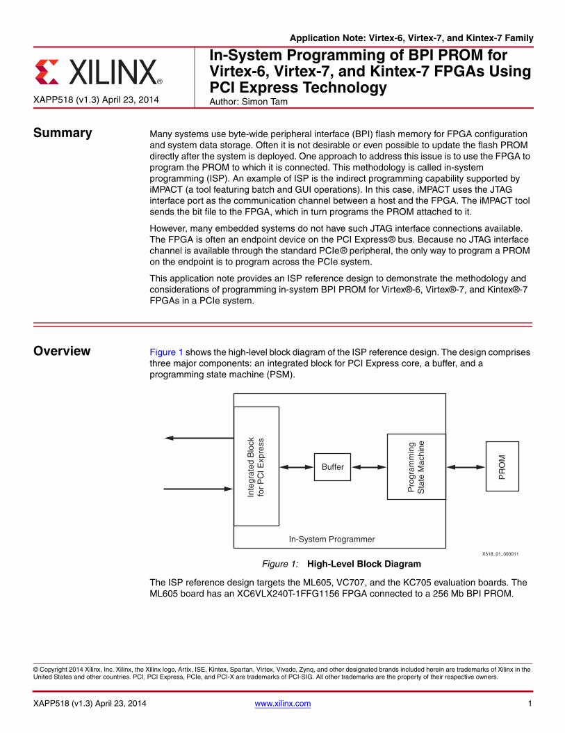
Overview Figure 1 shows the high-level block diagram of the ISP reference design. The design comprises three major components: an integrated block for PCI Express core, a buffer, and a programming state machine (PSM).
The ISP reference design targets the ML605, VC707, and the KC705 evaluation boards. The ML605 board has an XC6VLX240T-1FFG1156 FPGA connected to a 256 Mb BPI PROM.
Application Note: Virtex-6, Virtex-7, and Kintex-7 Family
XAPP518 (v1.3) April 23, 2014
In-System Programming of BPI PROM for Virtex-6, Virtex-7, and Kintex-7 FPGAs UsingPCI Express TechnologyAuthor: Simon Tam
X-Ref Target - Figure 1
Figure 1: High-Level Block Diagram
PR
OM
Pro
gram
min
gS
tate
Mac
hine
Inte
grat
ed B
lock
for
PC
I Exp
ress
Buffer
X518_01_093011
In-System Programmer
Integrated Block for PCI Express
XAPP518 (v1.3) April 23, 2014 www.xilinx.com 2
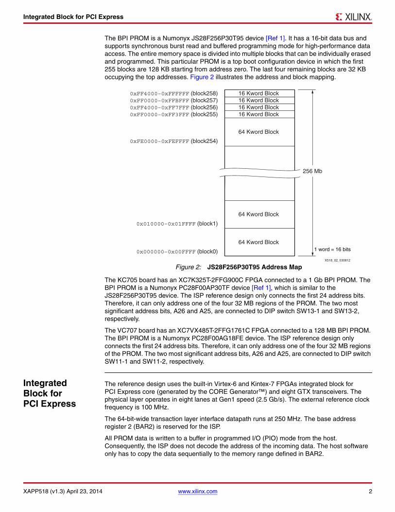
The BPI PROM is a Numonyx JS28F256P30T95 device [Ref 1]. It has a 16-bit data bus and supports synchronous burst read and buffered programming mode for high-performance data access. The entire memory space is divided into multiple blocks that can be individually erased and programmed. This particular PROM is a top boot configuration device in which the first 255 blocks are 128 KB starting from address zero. The last four remaining blocks are 32 KB occupying the top addresses. Figure 2 illustrates the address and block mapping.
The KC705 board has an XC7K325T-2FFG900C FPGA connected to a 1 Gb BPI PROM. The BPI PROM is a Numonyx PC28F00AP30TF device [Ref 1], which is similar to the JS28F256P30T95 device. The ISP reference design only connects the first 24 address bits. Therefore, it can only address one of the four 32 MB regions of the PROM. The two most significant address bits, A26 and A25, are connected to DIP switch SW13-1 and SW13-2, respectively.
The VC707 board has an XC7VX485T-2FFG1761C FPGA connected to a 128 MB BPI PROM. The BPI PROM is a Numonyx PC28F00AG18FE device. The ISP reference design only connects the first 24 address bits. Therefore, it can only address one of the four 32 MB regions of the PROM. The two most significant address bits, A26 and A25, are connected to DIP switch SW11-1 and SW11-2, respectively.
Integrated Block for PCI Express
The reference design uses the built-in Virtex-6 and Kintex-7 FPGAs integrated block for PCI Express core (generated by the CORE Generator™) and eight GTX transceivers. The physical layer operates in eight lanes at Gen1 speed (2.5 Gb/s). The external reference clock frequency is 100 MHz.
The 64-bit-wide transaction layer interface datapath runs at 250 MHz. The base address register 2 (BAR2) is reserved for the ISP.
All PROM data is written to a buffer in programmed I/O (PIO) mode from the host. Consequently, the ISP does not decode the address of the incoming data. The host software only has to copy the data sequentially to the memory range defined in BAR2.
X-Ref Target - Figure 2
Figure 2: JS28F256P30T95 Address Map
64 Kword Block
64 Kword Block
16 Kword Block16 Kword Block16 Kword Block16 Kword Block
0x000000–0x00FFFF (block0)
0x010000–0x01FFFF (block1)
0xFF0000–0xFF3FFF (block255)0xFF4000–0xFF7FFF (block256)0xFF0000–0xFFBFFF (block257)0xFF4000–0xFFFFFF (block258)
256 Mb
64 Kword Block
0xFE0000–0xFEFFFF (block254)
X518_02_030812
1 word = 16 bits

Buffer
XAPP518 (v1.3) April 23, 2014 www.xilinx.com 3
Figure 3 shows the simplified connections between the integrated block for PCI Express and the buffer FIFO on the receive path.
Buffer The buffer is implemented on a built-in FIFO in programmable logic and serves as a clock domain crossing buffer. One side of the FIFO is connected to the Integrated Block for PCI Express core clock domain operating at 250 MHz. The other side is connected to the PROM programmer clock domain at about 20 MHz. The FIFO size is 2 KB, which is twice the size of the PROM internal buffer used in buffered programming mode. The host application writes 64 bytes at a time, then waits until the PROM has completed programming the current set of data before writing another batch of data. Consequently, a data overflow situation should not occur. In addition, if the FIFO becomes close to full, it pauses the integrated block for PCI Express from providing more data as another safeguard to prevent data overflow.
Programming State Machine
The PSM is responsible for setting up and executing native PROM programming operations. Before the PROM program operation can begin, the entire target block in which the data is to be written must be erased. This process is the only way to change programmed bits to an unprogrammed state (or from 0 to 1). In addition, each block is in write protect mode by default. Therefore, it is necessary to unlock the target block before the erase command. The PSM supports the block-unlock and the erase command sequence.
X-Ref Target - Figure 3
Figure 3: Simplified Block Diagram between the FIFO and the Integrated Block for PCI Express
din[31:0]
Wr_enwr_clk
FIFO
Post_wr_data[31:0]
Write_en
wr_data_o[31:0] wr_data_i[31:0]
MEM_ACCESSRX ENGINE
Trn_rd[63:0] Trn_rd[63:0]
Integrated Block forPCI Express
wr_en_o
pause
pause
wr_busy_owr_busy_i
wr_en_oTrn_rdst_rdy_n
Trn_rdst_rdy_n
TX
RX
X518_03_093011
Programming State Machine
XAPP518 (v1.3) April 23, 2014 www.xilinx.com 4
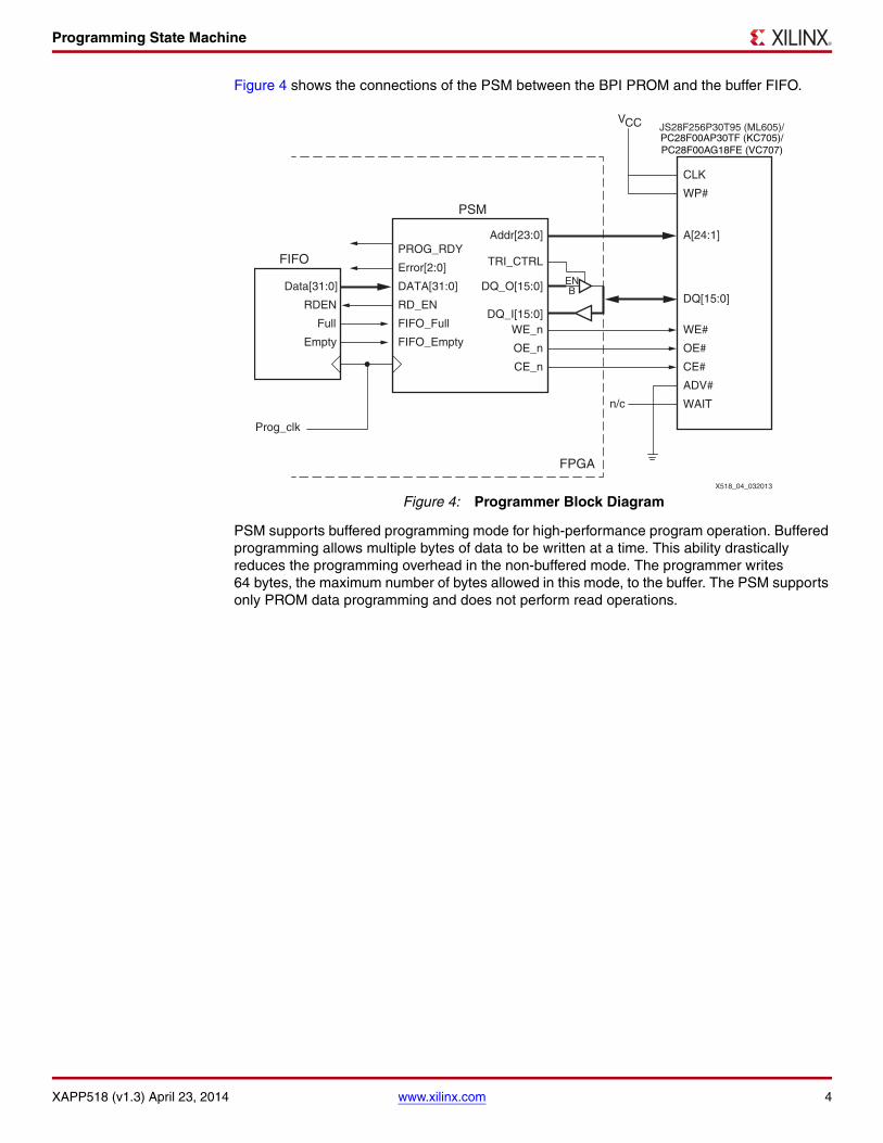
Figure 4 shows the connections of the PSM between the BPI PROM and the buffer FIFO.
PSM supports buffered programming mode for high-performance program operation. Buffered programming allows multiple bytes of data to be written at a time. This ability drastically reduces the programming overhead in the non-buffered mode. The programmer writes 64 bytes, the maximum number of bytes allowed in this mode, to the buffer. The PSM supports only PROM data programming and does not perform read operations.
X-Ref Target - Figure 4
Figure 4: Programmer Block Diagram
PSM
JS28F256P30T95 (ML605)/
A[24:1]
DQ[15:0]
WE#
OE#
CE#
Addr[23:0]
DQ_I[15:0]WE_n
OE_n
CE_n
WP#
ADV#
WAIT
CLK
n/c
V
Data[31:0]
RDEN
Full
Empty
DATA[31:0]
RD_EN
FIFO_Full
FIFO_Empty
Error[2:0]
PROG_RDY
DQ_O[15:0]
TRI_CTRL
ENB
Prog_clk
FPGA
FIFO
X518_04_032013
CCPC28F00AP30TF (KC705)/PC28F00AG18FE (VC707)

Programming State Machine
XAPP518 (v1.3) April 23, 2014 www.xilinx.com 5
The PSM consists of a main state machine with sub-loops responsible for each of the PROM programming native commands. Figure 5 shows the main command loop.
X-Ref Target - Figure 5
Figure 5: Main Command Loop
Idle
Unlock?
Erase?
Program?
FIFOEmpty?
Read a Wordfrom FIFO
StartAddress?
EndAddress?
Unlock Loop
Erase Loop
Program Loop
Register StartAddress
Register EndAddress
X518_05_022212
Y
Y
Y
Y
Y
Y
N
N
N
N
N
N
Programming State Machine
XAPP518 (v1.3) April 23, 2014 www.xilinx.com 6
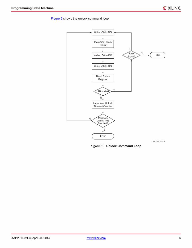
Figure 6 shows the unlock command loop.
X-Ref Target - Figure 6
Figure 6: Unlock Command Loop
Write x60 to DQ
Write xD0 to DQ
Write x90 to DQ
Read StatusRegister
SR = x80?
LastBlock?
MaximumUnlock TimeReached?
Error
Idle
N
Y
Y
N
N
Y
Increment UnlockTimeout Counter
X518_06_022212
Increment BlockCount

Programming State Machine
XAPP518 (v1.3) April 23, 2014 www.xilinx.com 7
Figure 7 shows the erase command loop.
X-Ref Target - Figure 7
Figure 7: Erase Command Loop
Erase loop
Write x50 to DQWrite Address
Write x20 to DQ
Write xD0 to DQ
Read StatusRegister
SR = x80?
LastBlock?
MaximumErase TimeReached?
Error = x3
Idle
N
Y
Y
N
N
Y
X518_07_090211
Increment EraseTimeout Counter
- Increment Block- Calculate Address
SR > x80? Error = x2
N
- Load First Block Number- Calculate Address
Y
Programming State Machine
XAPP518 (v1.3) April 23, 2014 www.xilinx.com 8
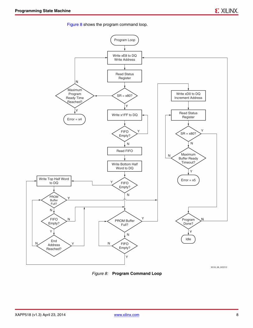
Figure 8 shows the program command loop.
X-Ref Target - Figure 8
Figure 8: Program Command Loop
Program Loop
Write xE8 to DQWrite Address
Write x1FF to DQ
FIFOEmpty?
N
Y
Y
N
Write Top Half Wordto DQ FIFO
Empty?
Y
N
SR = x80?
Read StatusRegister
MaximumProgram
Ready TimeReached?
Error = x4
Read FIFO
Write Bottom HalfWord to DQ
PROMBufferFull?
FIFOEmpty?
Read StatusRegister
N
EndAddress
Reached?
YN N
N
Write xD0 to DQIncrement Address
PROM BufferFull?
Y
FIFOEmpty?
Y
SR = x80?
ProgramDone?
Idle
MaximumBuffer Ready
Timeout?
Error = x5
Y
N
N
Y
X518_08_022212
N
N
YY
Y
Y

Programming State Machine
XAPP518 (v1.3) April 23, 2014 www.xilinx.com 9
Table 1 summarizes the recommended programming command sequence and definitions of each command.
Figure 9 and Figure 10 illustrate the timing diagrams at the beginning and ending of the buffer program stage.
Notes relevant to Figure 9:
1. CLK is the programmer module clock.
2. ADDR is the start address of the 256 words to be written in the PROM buffer.
3. The status output from the PROM is xx80.
Table 1: Host Software Command Sequence
Sequence Command Word Definition Notes
1 Start_Address 0x5341[aaaa] Specifies the starting block address.
2 End_Address 0x45[aaaaaa]Specifies the PROM word end address. Bits 23 to 0 of the command word define the end address.
3 Unlock 0x556E6C6BUnlocks contiguous blocks between the addresses specified in the Start_Address and End_Address commands.
4 Erase 0x45726173Erases contiguous blocks between the addresses specified in the Start_Address and End_Address commands.
5 Program 0x50726F67
Initiates the program sequence. The programmer reads data from the buffer and writes to the PROM until the end address is reached.
X-Ref Target - Figure 9
Figure 9: Buffered Programming Stage—Beginning
X518_09_091211
Addr + 1 Addr + 2 Addr + 3 Addr + 4
00E8 0000 01FF
D1D2D3D4
D2D1 D4D3
D5D6D7D8 D9D10D11D1250726F67
D6D5 D8D7 D10D9
CLK
A[23:0]
DQ[15:0]
WE_N
OE_N
TRI_CTRL
FIFO_RD_EN
FIFO_EMPTY
DATA[31:0]
PROG_RDY
Addr
xx80
000000
0000
XXXXXXXX

Programming State Machine
XAPP518 (v1.3) April 23, 2014 www.xilinx.com 10
Notes relevant to Figure 10:
1. CLK is the programmer module clock.
2. ADDR is the start address of the 256 words to be written in the PROM buffer.
3. The status outputs from the PROM are xx00 and xx80.
X-Ref Target - Figure 10
Figure 10: Buffered Programming Stage—Ending
CLK
A[23:0]
DQ[15:0]
WE_N
OE_N
TRI_CTRL
FIFO_RD_EN
FIFO_EMPTY
DATA[31:0]
Addr + 253
D1020D1019 D1022D1021 D1024D1023
Addr + 254 Addr + 255
00D0 0000 0000 00E8
Addr + 256Addr + 255Addr + 252
D1018D1017
D1017D1018D1019D1020D1021D1022D1023D1024 D1021D1022D1023D1024
0000
xx80xx00
X518_10_091211

Host Demonstration Software
XAPP518 (v1.3) April 23, 2014 www.xilinx.com 11
Host Demonstration Software
The reference design includes host software to facilitate the demonstration. The software comprises the demonstration application (shown in Figure 11) and drivers. The application’s Visual Basic 6 source code is provided in the reference design and is shown in Appendix A.
Note: The drivers are provided by Jungo [Ref 2], a third-party vendor. The reference design includes the drivers in binary format only. No driver source codes are provided. Contact Jungo directly for source code availability.
The application has two functional buttons:
• Erase All Blocks
• Program PROM
Clicking on the Erase All Blocks button erases every block in the PROM. After clicking on the Program PROM button, the user is asked to select a PROM file. The application then executes a series of native PROM commands to program the PROM from the data in the user PROM file. The function status and progress are displayed in the console log window. An excerpt of the source code’s program PROM function is listed in Appendix A.
PROM Function Stages
The program PROM function has three major sections:
• File Parsing
• Program Setup
• PROM Programming
X-Ref Target - Figure 11
Figure 11: XAPP518 Demo Application WindowX518_12_091311

Host Demonstration Software
XAPP518 (v1.3) April 23, 2014 www.xilinx.com 12
File Parsing
During the file parsing stage, the application reads through the entire PROM file to determine the starting and ending extended linear address (ELA) and calculates the PROM data size. Figure 12 shows the flow diagram.
X-Ref Target - Figure 12
Figure 12: File Parsing Flow Diagram
<PROM>.mcs Open PROM File
EOF?
Read a Line from File
Record Last ELA
ExtendedAddress Record?
Start BlockDefined?
Record Start ELA
Data Record?Close File
Record LastAddress
Command Loop
X518_13_090211

Host Demonstration Software
XAPP518 (v1.3) April 23, 2014 www.xilinx.com 13
Program Setup
The program setup stage issues unlock, erase, and program commands to prepare for the subsequent programming operations, as shown in Figure 13.
X-Ref Target - Figure 13
Figure 13: Program Setup Flow Diagram
X518_14_090211
Calculate File Size
Calculate File StartAnd End Blocks
Write StartAddr toBuffer
Write EndAddr toBuffer
Write UnlockCommand to Buffer
Write EraseCommand to Buffer
Read Ready Status
Ready?
Read Ready Status
Ready?
Memory Copy
Memory Copy
Write ProgramCommand to Buffer
Memory Copy
Program
Program Setup
N Y
Y
N

Host Demonstration Software
XAPP518 (v1.3) April 23, 2014 www.xilinx.com 14
PROM Programming
The PROM programing stage reads 64 sequential bytes of data from the PROM file at a time, fills up a local buffer, and copies the buffer data to the programmer target address (Figure 14). The monitoring routine polls the programmer ready status and repeats the program process until the last byte of PROM data is written.
X-Ref Target - Figure 14
Figure 14: PROM Programming Flow Diagram
Open PROM File
EOF?
Read ProgrammerStatus
Status =Ready?
Update Word Count
32 WordsWritten?
Read a Line fromFile
RecordType =EOF?
Exit
RecordType =Data?
Write AvailableData to Buffer
Status =Program Error?
Close File
Copy 64 Bytesto Target
N
Exit
N
Y
Y
N
Y
Y
N
N
N
Y
X518_15_022212
Y
MCS PROM File Format
XAPP518 (v1.3) April 23, 2014 www.xilinx.com 15
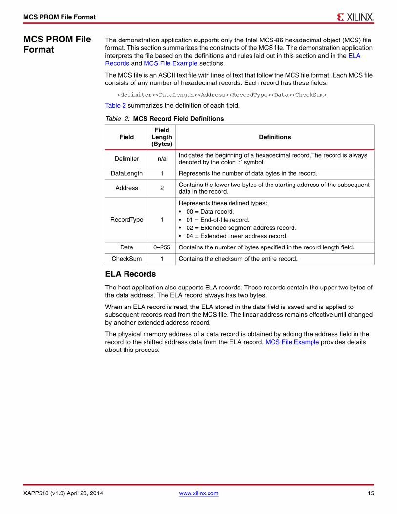
MCS PROM File Format
The demonstration application supports only the Intel MCS-86 hexadecimal object (MCS) file format. This section summarizes the constructs of the MCS file. The demonstration application interprets the file based on the definitions and rules laid out in this section and in the ELA Records and MCS File Example sections.
The MCS file is an ASCII text file with lines of text that follow the MCS file format. Each MCS file consists of any number of hexadecimal records. Each record has these fields:
<delimiter><DataLength><Address><RecordType><Data><CheckSum>
Table 2 summarizes the definition of each field.
ELA Records
The host application also supports ELA records. These records contain the upper two bytes of the data address. The ELA record always has two bytes.
When an ELA record is read, the ELA stored in the data field is saved and is applied to subsequent records read from the MCS file. The linear address remains effective until changed by another extended address record.
The physical memory address of a data record is obtained by adding the address field in the record to the shifted address data from the ELA record. MCS File Example provides details about this process.
Table 2: MCS Record Field Definitions
FieldField
Length (Bytes)
Definitions
Delimiter n/a Indicates the beginning of a hexadecimal record.The record is always denoted by the colon ‘:’ symbol.
DataLength 1 Represents the number of data bytes in the record.
Address 2 Contains the lower two bytes of the starting address of the subsequent data in the record.
RecordType 1
Represents these defined types:• 00 = Data record.• 01 = End-of-file record.• 02 = Extended segment address record.• 04 = Extended linear address record.
Data 0–255 Contains the number of bytes specified in the record length field.
CheckSum 1 Contains the checksum of the entire record.
MCS PROM File Format
XAPP518 (v1.3) April 23, 2014 www.xilinx.com 16
MCS File Example
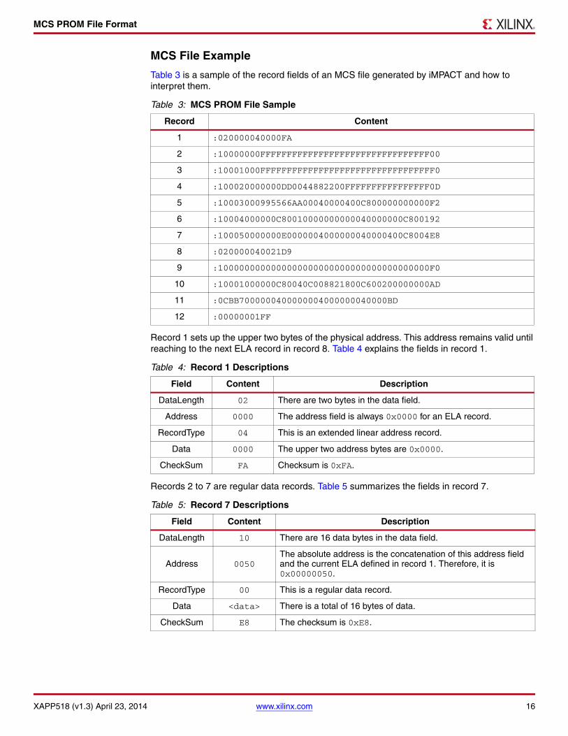
Table 3 is a sample of the record fields of an MCS file generated by iMPACT and how to interpret them.
Record 1 sets up the upper two bytes of the physical address. This address remains valid until reaching to the next ELA record in record 8. Table 4 explains the fields in record 1.
Records 2 to 7 are regular data records. Table 5 summarizes the fields in record 7.
Table 3: MCS PROM File Sample
Record Content
1 :020000040000FA
2 :10000000FFFFFFFFFFFFFFFFFFFFFFFFFFFFFFFF00
3 :10001000FFFFFFFFFFFFFFFFFFFFFFFFFFFFFFFFF0
4 :100020000000DD0044882200FFFFFFFFFFFFFFFF0D
5 :10003000995566AA00040000400C800000000000F2
6 :10004000000C80010000000000040000000C800192
7 :100050000000E0000004000000040000400C8004E8
8 :020000040021D9
9 :1000000000000000000000000000000000000000F0
10 :10001000000C80040C008821800C600200000000AD
11 :0CBB7000000400000004000000040000BD
12 :00000001FF
Table 4: Record 1 Descriptions
Field Content Description
DataLength 02 There are two bytes in the data field.
Address 0000 The address field is always 0x0000 for an ELA record.
RecordType 04 This is an extended linear address record.
Data 0000 The upper two address bytes are 0x0000.
CheckSum FA Checksum is 0xFA.
Table 5: Record 7 Descriptions
Field Content Description
DataLength 10 There are 16 data bytes in the data field.
Address 0050The absolute address is the concatenation of this address field and the current ELA defined in record 1. Therefore, it is 0x00000050.
RecordType 00 This is a regular data record.
Data <data> There is a total of 16 bytes of data.
CheckSum E8 The checksum is 0xE8.

Reference Design Demonstration
XAPP518 (v1.3) April 23, 2014 www.xilinx.com 17
Record 8 updates the upper two bytes of the physical address. This address remains valid for the rest of the file. Table 6 describes the fields in the record.
Records 9 to 11 are regular data records. Record 11 is the last data record and often has a number of data bytes fewer than 16 bytes. Table 7 summarizes the fields in record 11.
Reference Design Demonstration
This section guides the user through setting up and running the reference design demonstration. The demonstration allows users to program the BPI PROM on a ML605, VC707, or KC705 board connected to a host system running Windows XP. Pre-built bit files and host software applications are available in the reference design.
System Requirements
These are required for the demonstration:
• ML605 demonstration platform (XC6VLX240T-FF1156 production device), VC707 evaluation board (XC7VX485T-2FFG1761C), or KC705 evaluation board (XC7K325T-2FFG900C)
• X86 system with Windows XP Service Pack 3 installed
Use these steps to run the reference design demonstration:
1. Extract the ML605.zip, VC707.zip, or the KC705.zip inside the xapp518.zip file to the <ref_design_dir> directory.
2. Copy all files in <ref_design_dir>\sw\Jungo\system to <WindowsXP_install_path>\system32.
This step installs the Jungo WinDriver libraries and driver (rev. 10.2) in Windows XP. COMDLD32.OCX should be backed up if the file already exists.
3. Set DIP switch on the board as follows to enable BPI flash programming:
• For the ML605 board:
- S2-1 = ON
- S2-2 = ON
Table 6: Record 8 Descriptions
Field Content Description
DataLength 02 There are two data bytes in the data field.
Address 0000 The address field is always 0x0000 for an ELA record.
RecordType 04 This is an ELA record.
Data 0021 The upper two address bytes are 0x0000.
CheckSum D9 Checksum is 0xD9.
Table 7: Record 11 Descriptions
Field Content Description
DataLength 0C There are 12 data bytes in the data field.
Address BB70The absolute address is the concatenation of this address field and the current ELA defined in record 1. Therefore, it is 0x0021BB70.
RecordType 00 This is a regular data record.
Data <data> There are 12 bytes of data.
CheckSum E8 Checksum is 0xBD.

Reference Design Demonstration
XAPP518 (v1.3) April 23, 2014 www.xilinx.com 18
- S2-3 = OFF
- S2-4 = ON
- S2-5 = ON
- S2-6 = OFF
• For the VC707 board:
- S11-1 = OFF
- S11-2 = OFF
- S11-3 = OFF
- S11-4 = ON
- S11-5 = OFF
• For the KC705 board:
- S13-1 = OFF
- S13-2 = OFF
- S13-3 = OFF
- S13-4 = ON
- S13-5 = OFF
4. Set DIP switch as follows to avoid loading from the CompactFlash card (ML605 board only):
• S1-1 = OFF
• S1-2 = OFF
• S1-3 = OFF
• S1-4 = OFF
5. Plug in the board to an available PCIe device slot in a host system:
a. For the ML605 board:
- Connect the Advanced Technology eXtended (ATX) power cable to J25.
- Set switch SW2 to the ON position.
b. For the VC707 board:
- Connect the 6-pin mini-fit connector J18 to a compatible power source.
- Set switch SW12 to the ON position.
c. For the KC705 board:
- Connect the 6-pin mini-fit connector J49 to a compatible power source.
- Set switch SW15 to the ON position.
6. Turn on the system.
The demonstration application can program the P30 BPI PROM starting from any address within the PROM address range. These steps describe the procedure to create a PROM file starting from a designated start address:
7. Use the PROMGen command options in Table 8 to create a PROM file for the application.
Table 8: PROMGen Options
Option Comments
-s <PROM size> Size must be a power of 2
-p <format> Only MCS format is supported by the application
-data_width The target PROM data width is 16

Reference Design Demonstration
XAPP518 (v1.3) April 23, 2014 www.xilinx.com 19
8. Enter the following command line in a shell or command prompt. This command creates an MCS format file from a bit file <user_bit_file> that targets a 32 MB BPI PROM at start address 0x800000.
promgen -w -s 32768 -p mcs -data_width 16 -o <PROM_File.mcs> -u 0x800000 <user bit_file>
9. Run the following command to convert the file to a MS-DOS compatible format.
unix2dos <PROM_File.mcs>
Note: The demonstration application cannot correctly read the MCS file created by promgen due to the line wrap convention. The demonstration application hangs if the PROM file is not in DOS compatible format. It is recommended to convert the line wraps by shareware program such as unix2dos (available on many public shareware web sites).
The subsequent steps configure the FPGA to enable the BPI programmer reference design.
10. Connect cables:
a. For the ML605 board:
- Connect the mini-USB cable connector to the J22 connector, and connect the other end to a USB connector to the host system.
b. For the VC707 board:
- Connect the Platform Cable USB II connector between the J4 board and the host system.
c. For the KC705 board:
- Connect the Platform Cable USB II connector between the J60 board and the host system.
11. Launch iMPACT and select the Boundary Scan flow.
12. Click the Initialize Chain button.
13. Right-click the FPGA in the scan chain and select Assign New Configuration File.
a. For the ML605 board, select: <ref_design_dir>\config\bitfile\PCIe_ISP_top_ML605.bit
a. For the VC707 board, select: <ref_design_dir>\config\bitfile\PCIe_ISP_top_VC707.bit
b. For the KC705 board, select: <ref_design_dir>\config\bitfile\PCIe_ISP_top_KC705.bit
The resulting iMPACT screen for the ML605 board should appear as shown in Figure 15.
-o PROM file name
-u Start address
Table 8: PROMGen Options
Option Comments

Reference Design Demonstration
XAPP518 (v1.3) April 23, 2014 www.xilinx.com 20
X-Ref Target - Figure 15
Figure 15: Assign Configuration File to the FPGA Device
X518_16_092111

Reference Design Demonstration
XAPP518 (v1.3) April 23, 2014 www.xilinx.com 21
14. Right-click the FPGA again and select Program. This step configures the BPI programmer in the FPGA, and the iMPACT screen shown in Figure 16 appears when the step is completed successfully.
Note: For ML605: the MMCM locked (DS21) and link ready (DS22) LEDs are turned on. For VC707: LEDs DS0, DS1, and DS2 are turned on. LED DS3 will blink. For KC705: LEDs DS0, DS1, and DS2 are turned on. The LED DS3 will blink.
15. Restart the host system.
Caution! Do not turn off and turn back on the system. The warm restart is necessary for the host system to discover and enumerate the newly configured function (the BPI programmer).
These steps describe how to set up and use the demonstration application to program the BPI PROM from the host system:
X-Ref Target - Figure 16
Figure 16: FPGA Configuration Succeeded
X518_17_092111
Reference Design Demonstration
XAPP518 (v1.3) April 23, 2014 www.xilinx.com 22
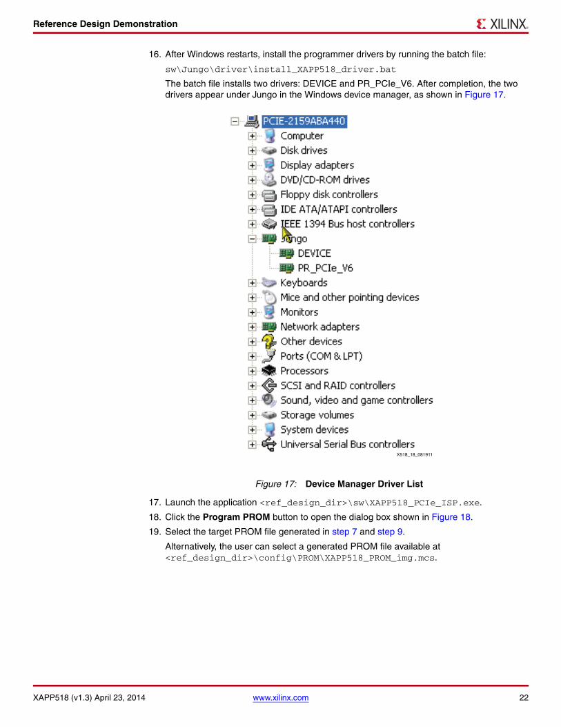
16. After Windows restarts, install the programmer drivers by running the batch file:
sw\Jungo\driver\install_XAPP518_driver.bat
The batch file installs two drivers: DEVICE and PR_PCIe_V6. After completion, the two drivers appear under Jungo in the Windows device manager, as shown in Figure 17.
17. Launch the application <ref_design_dir>\sw\XAPP518_PCIe_ISP.exe.
18. Click the Program PROM button to open the dialog box shown in Figure 18.
19. Select the target PROM file generated in step 7 and step 9.
Alternatively, the user can select a generated PROM file available at<ref_design_dir>\config\PROM\XAPP518_PROM_img.mcs.
X-Ref Target - Figure 17
Figure 17: Device Manager Driver List
X518_18_081911
Reference Design Demonstration
XAPP518 (v1.3) April 23, 2014 www.xilinx.com 23
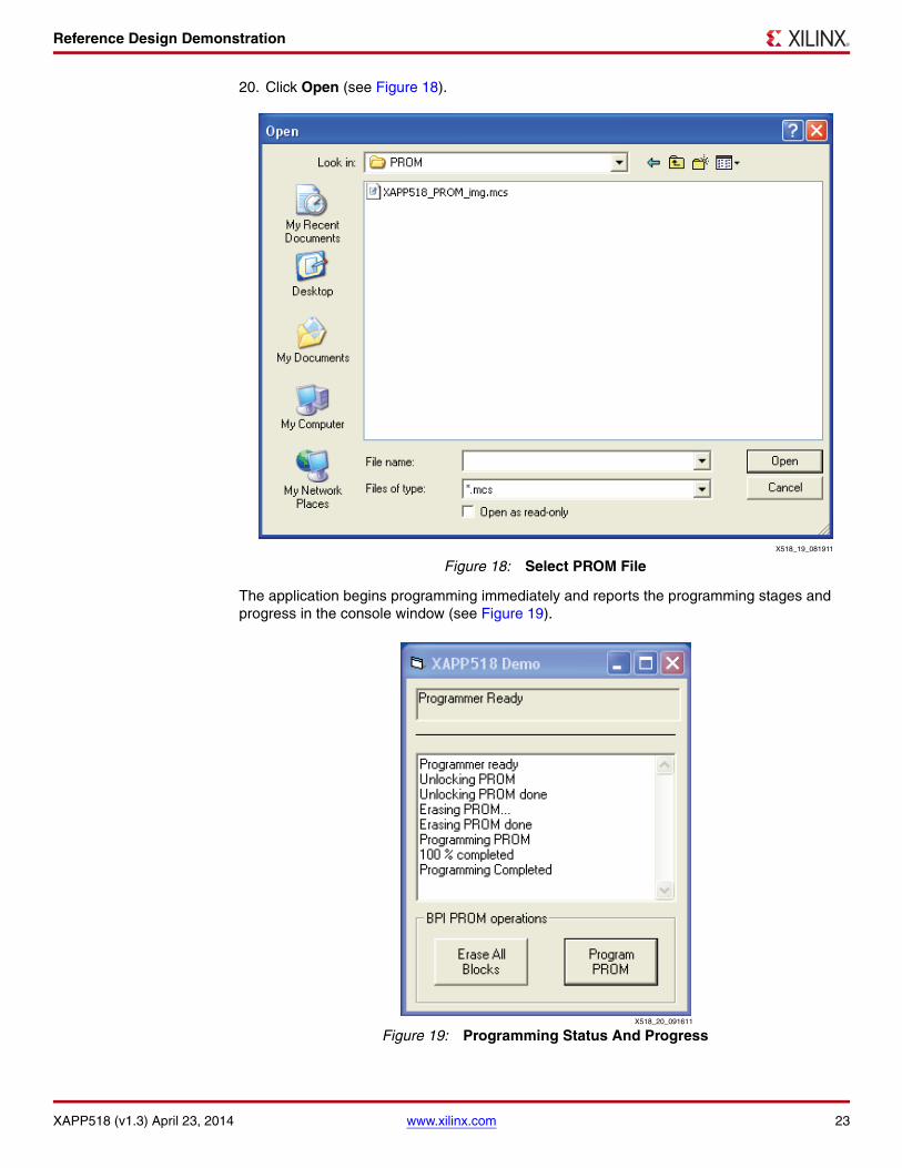
20. Click Open (see Figure 18).
The application begins programming immediately and reports the programming stages and progress in the console window (see Figure 19).
X-Ref Target - Figure 18
Figure 18: Select PROM File
X-Ref Target - Figure 19
Figure 19: Programming Status And Progress
X518_19_081911
X518_20_091611

Reference Design Demonstration
XAPP518 (v1.3) April 23, 2014 www.xilinx.com 24
After programming the PROM, the user can independently confirm that the programmed contents are correct by using iMPACT to verify the PROM contents. These steps describe how to set up iMPACT to go through the verification:
21. Launch iMPACT and select Boundary Scan flow again.
22. Click OK.
23. Right-click the target FPGA.
24. Select Add SPI/BPI Flash, as shown in Figure 20.X-Ref Target - Figure 20
Figure 20: Add BPI Flash in iMPACT
X518_21_081911
Reference Design Demonstration
XAPP518 (v1.3) April 23, 2014 www.xilinx.com 25
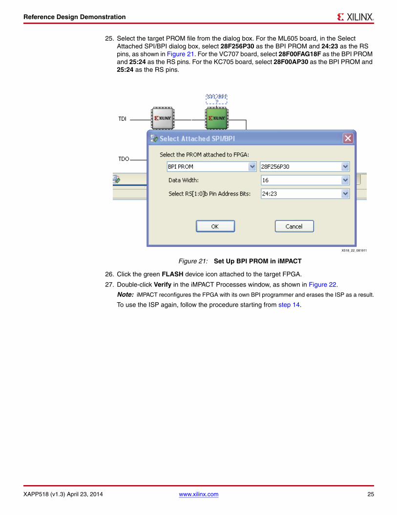
25. Select the target PROM file from the dialog box. For the ML605 board, in the Select Attached SPI/BPI dialog box, select 28F256P30 as the BPI PROM and 24:23 as the RS pins, as shown in Figure 21. For the VC707 board, select 28F00FAG18F as the BPI PROM and 25:24 as the RS pins. For the KC705 board, select 28F00AP30 as the BPI PROM and 25:24 as the RS pins.
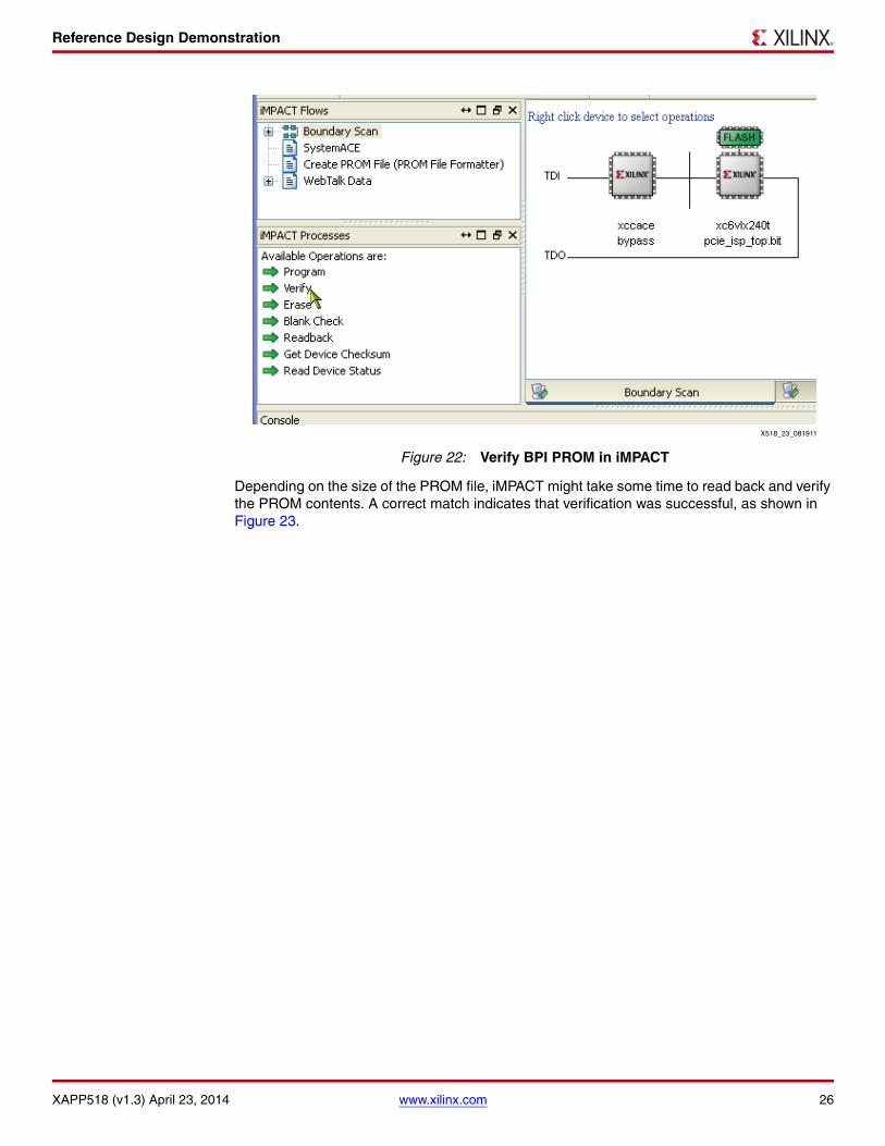
26. Click the green FLASH device icon attached to the target FPGA.
27. Double-click Verify in the iMPACT Processes window, as shown in Figure 22.
Note: iMPACT reconfigures the FPGA with its own BPI programmer and erases the ISP as a result.
To use the ISP again, follow the procedure starting from step 14.
X-Ref Target - Figure 21
Figure 21: Set Up BPI PROM in iMPACT
X518_22_081911
Reference Design Demonstration
XAPP518 (v1.3) April 23, 2014 www.xilinx.com 26
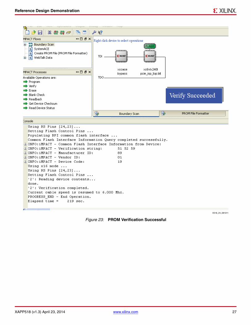
Depending on the size of the PROM file, iMPACT might take some time to read back and verify the PROM contents. A correct match indicates that verification was successful, as shown in Figure 23.
X-Ref Target - Figure 22
Figure 22: Verify BPI PROM in iMPACT
X518_23_081911
Reference Design Demonstration
XAPP518 (v1.3) April 23, 2014 www.xilinx.com 27
X-Ref Target - Figure 23
Figure 23: PROM Verification Successful
X518_24_081911

Failsafe PROM Update
XAPP518 (v1.3) April 23, 2014 www.xilinx.com 28
Failsafe PROM Update
Problems can occur during the PROM update process. For example, the system power might be interrupted or the PROM data are corrupted while the new configuration bitstream is being updated in the PROM. The result is that the FPGA cannot configure properly from the PROM after such failed PROM update event. A failsafe methodology needs to be in place to ensure the continued operation and recovery of the system.
One method to address the potential issue is to use the FPGA configuration fallback feature. Fallback is control logic that ensures the FPGA is always configured with a default PROM image if there is an error during the configuration process. Such user default system has minimal features with the sole purpose to recover from configuration failure.
During configuration, these errors can trigger fallback: an IDCODE error, a CRC error, a Watchdog Timer timeout error, or a BPI address wraparound error. After configuration, the Watchdog Timer, enabled in the user monitor mode, can also trigger fallback. If fallback reconfiguration fails a second time, configuration stops and both INIT_B and DONE are held Low. Fallback can also be disabled with BitGen option -g ConfigFallback:Disable.
During fallback reconfiguration, the FPGA drives new values on the two dual-mode pins RS[1:0] (revision select). RS[1:0] are in high-impedance state and weakly pulled up during the first configuration, and weakly pulled down after configuration by default. The user can use external pull-up/pull-down resistors to override the FPGA weak pull-up resistor during first configuration to load the desired bitstream. When a configuration error is detected, the configuration logic generates an internal reset pulse and actively drives RS[1:0] to 00 for loading the fallback bitstream.
The ML605 board can demonstrate fallback configuration. For example, let the onboard BPI PROM be divided into two halves of equal size containing two images—a user function image and a fallback image. The user function image has the bitstream of intended normal operation and should be stored in the upper half of the PROM address range. The fallback image has the golden bitstream that is for recovery after an unsuccessful configuration event and should be stored in the lower half of the PROM address range. Figure 24 shows the PROM address mapping.
X-Ref Target - Figure 24
Figure 24: PROM Address Map
XAPP518_30_061312
User FunctionImage
0xFFFFFF
0x800000
PR
OM
Wor
d A
ddre
ss
0x0
FallbackImage

Failsafe PROM Update
XAPP518 (v1.3) April 23, 2014 www.xilinx.com 29
One of the FPGA revision select pins, RS[0], is connected to the most significant address bit (A[24] pin) of the PROM shown in Figure 25 (RS[1] is not connected). A[24] is connected to DIP switch S2-6 through a weak pull-up resistor.
When the configuration mode is set to master BPI-up mode, the BPI address pin Addr[22:0] is set to logic zero upon power-up. If DIP switch S2-6 is closed, the address presented to the PROM is 0x800000. Therefore, the FPGA begins loading the configuration bitstream from the upper memory region starting from address 0x800000 where the user configuration bitstream is located.
If there is any error event during configuration it triggers fallback configuration. The internal configuration logic drives the RS[0] pin and BPI address pins Addr[22:0] to all zeros, effectively pointing the PROM address to 0x0. It then restarts the configuration process starting from 0x0 loading the fallback bitstream.
Fallback Demonstration
These steps demonstrate the fallback feature on the ML605 board:
1. Set DIP switch S2 on the ML605 board as follows to enable BPI PROM programming:
• S2-1 = ON
• S2-2 = ON
• S2-3 = OFF
• S2-4 = ON
• S2-5 = ON
• S2-6 = OFF
• S1-1 = OFF
• S1-2 = OFF
• S1-3 = OFF
• S1-4 = OFF
2. Launch the application <ref_design_dir>\sw\XAPP518_PCIe_ISP.exe.
3. Click the Program PROM button. Select a pre-made PROM file available at <ref_design_dir>\config\PROM\XAPP518_corrupted_PROM_img.mcs.
4. Click Open.
This MCS file is a corrupted image file and causes configuration failure during loading. The start address of this particular image file is 0x800000.
X-Ref Target - Figure 25
Figure 25: ML605 Revision Select Pin ConnectionXAPP518_31_061312
BPI PROM
FPGA
Data[15:0]
A[23:1]
A[24]
n/c
Data[15:0]
Addr[22:0]
RS[1]
RS[0]
Mode[2]Mode[1]Mode[0]
VccVcc
S2-6

Failsafe PROM Update
XAPP518 (v1.3) April 23, 2014 www.xilinx.com 30
5. Click the Program PROM button again. Select a pre-made PROM file available at <ref_design_dir>\config\PROM\XAPP518_fallback_PROM_img.mcs.
6. Click Open.
This MCS file is the fallback image file and contains a simple design that turns on all user LEDs on the ML605 board. The start address of this particular image file is 0x0.
At this point the PROM has the user function bitstream located in the upper half of the PROM and the fallback bitstream in the lower half.
7. Set DIP switch S2 on the ML605 board as follows to enable master BPI-up configuration:
• S2-1 = OFF
• S2-2 = ON
• S2-3 = OFF
• S2-4 = ON
• S2-5 = OFF
• S2-6 = ON
8. Recycle power of the host system.
The FPGA first loads the user function bitstream from PROM address 0x800000. Because the bitstream is corrupted, the configuration fails on CRC error. A short time after power-up, the INIT LED flashes momentarily, indicating configuration error. The FPGA then triggers fallback configuration. The FPGA loads the fallback bitstream from PROM address 0x0. After completing the fallback configuration, the fallback design illuminates all user LEDs on the ML650 board.

Building the Reference Design
XAPP518 (v1.3) April 23, 2014 www.xilinx.com 31
Building the Reference Design
These steps describe how to build the reference design:
1. Extract the contents of the reference design ZIP file, ML605.zip, VC707.zip, or KC705.zip, inside the xapp518.zip file to a user directory <ref_design_dir>.
2. Open design project file <ref_design_dir>\hw\ISE\PCIe_ISP\PCIe_ISP.xise. The project should appear as shown in Figure 26.
3. Select the design top-level module PCIe_ISP_top in the Hierarchy pane.
X-Ref Target - Figure 26
Figure 26: Project Design View in Project Navigator
X518_25_022712
Building the Reference Design
XAPP518 (v1.3) April 23, 2014 www.xilinx.com 32
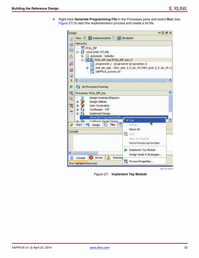
4. Right-click Generate Programming File in the Processes pane and select Run (see Figure 27) to start the implementation process and create a bit file.
X-Ref Target - Figure 27
Figure 27: Implement Top Module
X518_26_022712

Reference Design
XAPP518 (v1.3) April 23, 2014 www.xilinx.com 33
Reference Design
The reference design files for this application note can be downloaded at:
https://secure.xilinx.com/webreg/clickthrough.do?cid=184933
Table 9 shows the reference design matrix.
Design Advisory
Users should read these guidelines before adopting the reference design in their own projects:
• The reference design does not program the last four 16 Kword blocks.
• This reference design demonstrates the front-to-back flow and mechanism to program a BPI PROM via PCIe technology in FPGAs. In real situations, the programming function needs to share the PCIe bus with the user functions, that is, design integration is needed. Sharing of the PCIe interface between the user and PROM programming mode must also be managed. This sharing falls under the user hardware design and software control and is beyond the scope of this reference design.
Table 9: Reference Design Matrix
Reference Design Matrix
General
Developer Name Xilinx
Target Devices (Stepping Level, ES, Production, Speed Grades) Virtex-6 FPGA(XC6VLX240T-FF1156-1)Virtex-7 FPGA (XC7VX485T-2FFG1761C) Kintex-7 FPGA (XC7K325T-2FFG900C)
Source Code Provided? Yes
Source Code Format Verilog
Design Uses Code or IP from Existing Reference Design, Application Note, Third-Party, or CORE Generator™ tool?
Yes
Simulation
Functional Simulation Performed? Yes
Timing Simulation Performed? No
Test bench Provided for Functional and Timing Simulations? No
Test bench Format Verilog
Simulator Software and Version ModelSim SE 6.4b
SPICE/IBIS Simulations? No
Implementation
Synthesis Software Tools and Version XST 14.4
Implementation Software Tools and Version ISE® Design Suite 14.4
Static Timing Analysis Performed? Yes
Hardware Verification
Hardware Verified? Yes
Hardware Platform Used for Verification ML605 Rev. D board, VC707 Rev. B board, and KC705 Rev. D board

Resource Utilization
XAPP518 (v1.3) April 23, 2014 www.xilinx.com 34
• Although the PCIe bus can sustain relatively high throughput even in PIO mode (~20 MB/s), the overall system performance is limited by the BPI PROM interface performance. The PROM erase and program times make up the significant parts of the total programming time.
• This reference design was tested only in Gen1 x8 configuration.
• The reference design supports only 32-word buffered programming mode to be backward compatible with older technology PROMs. Some newer P30 PROMs can support 1,024-word buffered programming mode. The buffer size in the HDL should be adjusted to take advantage of the performance.
Resource Utilization
Table 10 shows the resource utilization for the reference design.
Performance System performance depends on many factors such as the host bus, software application, and PROM programming throughput. User design performance can vary significantly from this demonstration. On average, this design can program a 25 MB PROM file in 96 seconds from start to finish on a system similar to the one listed in Tested Systems, page 34.
Tested Systems The reference design was tested in these host system environments:
• ASUS P5B-VM:
• CPU: Pentium 4 531 (3.0 GHz)
• Chipset: Intel P965/G965
• Southbridge: Intel 828011HB/HR (ICH8/R)
• Intel desktop D975XBX:
• CPU: Pentium D (3.0 GHz)
• Chipset: Intel 975 Express Chipset
• Southbridge: Intel 82801GR (ICH7R)
• http://www.micron.com/~/media/Documents/Products/Data%20Sheet/NOR%20Flash/Parallel/P30/208033_P30_65nm_SBC_64M_128M_Discrete_DS.pdf
References This application note uses these references:
1. Numonyx Axcell Flash Memory (P30-65 nm) data sheetwww.micron.com
2. Jungo, www.jungo.com
3. UG517, Virtex-6 FPGA Integrated Block for PCI Express User Guide
Table 10: Resource Utilization
Resources XC6VLX240T Usage XC7VX485T Usage XC7K325T Usage
LUTs 1,325 1,346 1,580
Registers 1,158 2,846 2,847
Block RAMs/FIFO 9 9 9

Appendix A
XAPP518 (v1.3) April 23, 2014 www.xilinx.com 35
Appendix A This appendix contains the Visual Basic 6 function responsible for programming the flash PROM.
Dim pData As LongDim Commands(2) As LongDim CmdUnlock, CmdErase, CmdProgram, ReadData As LongDim File_Name As StringDim fnum, fnum_read As IntegerDim ReadMask, CmpVal As LongDim LineFile As StringDim RecType, RecLength, RecAddr As LongDim byte_cnt As IntegerDim StartBlockSet As BooleanDim StartBlock, EndBlock, LastAddr As StringDim RecData As StringDim DataOut(511) As LongDim LoopNumber As LongLoopNumber = 16Dim i, j As IntegerDim FileSize, ProgressCount As LongDim StartAddr_cmd As StringDim StartBlock_w, StartAddr, EndAddr_cmd As LongDim TextPos As Integer
CmdUnlock = &H556E6C6B 'Unlock commandCmdErase = &H45726173 'Erase commandCmdProgram = &H50726F67'Program commandStartBlockSet = False
On Error GoTo ErrHandle 'obtain pointer to the hardware from driverpData = (hML507_MK.cardReg.Card.Item(hML507_MK.addrDesc(ML507_MK_AD_BAR2).Index).dw4) With ComDiagRead .Filter = "*.mcs|*.mcs" .CancelError = True .ShowOpen End With File_Name = ComDiagRead.FileName fnum = FreeFile Open File_Name For Input As fnum
'Calculate the total number of PROM blocks targetted
While Not EOF(fnum) Line Input #fnum, LineFile 'read a line from the PROM file RecType = Mid(LineFile, 8, 2) If RecType = 4 Then 'Extended Address record type? If StartBlockSet <> True Then StartBlock = Mid(LineFile, 10, 4) StartBlockSet = True Else EndBlock = Mid(LineFile, 10, 4) End If Else If RecType = 0 Then 'Data record type? LastAddr = Mid(LineFile, 4, 4) End If End If
Appendix A
XAPP518 (v1.3) April 23, 2014 www.xilinx.com 36
Wend Close fnum 'close file
'Calculate file size
StartBlock_w = Val("&h" & StartBlock) / 2 If StartBlock_w <= 15 Then StartAddr_cmd = "0" & Hex(StartBlock_w) & "00" 'address in PROM word Else StartAddr_cmd = Hex(StartBlock_w) & "00" 'address in PROM words End If EndAddr_cmd = Val("&h" & EndBlock & LastAddr) / 2 'address in PROM words StartAddr = Val("&h" & StartBlock & "0000") / 2 FileSize = EndAddr_cmd - StartAddr 'file size in bytes ReadMask = "&h00008000" Call memcpy(VarPtr(ReadData), pData, 4) 'read programmer status CmpVal = ReadMask And ReadData If CmpVal = 32768 Then Text1.Text = "Programmer ready" & vbCrLf Else Text1.Text = "Programmer initialization error!" & vbCrLf Exit Sub End If Text1.SelStart = Len(Text1.Text) Text1.SelText = "Unlocking PROM" & vbCrLf ' Unlock blocks for erase Commands(0) = "&h" & "5341" & StartAddr_cmd 'start address Commands(1) = "&h" & "45" & Hex(EndAddr_cmd) 'end address Commands(2) = CmdUnlock 'unlock command Call memcpy(pData, VarPtr(Commands(0)), 12) 'issue commands to the target CmpVal = 0 While Not CmpVal = 32768 'Poll Programmer ready status Call memcpy(VarPtr(ReadData), pData, 4) CmpVal = ReadMask And ReadData Wend Text1.SelStart = Len(Text1.Text) Text1.SelText = "Unlocking PROM done" & vbCrLf & "Erasing PROM..." & vbCrLf
'Erase blocks Commands(0) = CmdErase 'Erase command Call memcpy(pData, VarPtr(Commands(0)), 4) CmpVal = 0 While Not CmpVal = 32768 'Poll Programmer ready status Call memcpy(VarPtr(ReadData), pData, 4) CmpVal = ReadMask And ReadData Wend Text1.SelStart = Len(Text1.Text) Text1.SelText = "Erasing PROM done" & vbCrLf & "Programming PROM" & vbCrLf

Appendix A
XAPP518 (v1.3) April 23, 2014 www.xilinx.com 37
' Already reached EOF. Need to reopen the file to reset sequential read pointer fnum = FreeFile 'grab a new free file number again Open File_Name For Input As fnum 'Send out the Program command Commands(0) = CmdProgram Call memcpy(pData, VarPtr(Commands(0)), 4)
TextPos = Len(Text1.Text) Text1.SelStart = TextPos
ProgressCount = 0ReadMask = "&h000000FF" 'change read mask to filter the lowest byte While Not EOF(fnum) i = 0 'check status Call memcpy(VarPtr(ReadData), pData, 4) CmpVal = ReadMask And ReadData If CmpVal = 128 Then ProgressCount = ProgressCount + 32 '32 words at a time Text1.SelStart = TextPos Text1.SelLength = 15 Text1.SelText = (Math.Round(ProgressCount / FileSize * 100)) & " % completed"
Do While i < LoopNumber Line Input #fnum, LineFile RecLength = Val("&h" & Mid(LineFile, 2, 2)) RecType = Mid(LineFile, 8, 2) RecData = Mid(LineFile, 10, 32) byte_cnt = RecLength / 4 If RecType = 1 Then 'end-of-file record? Exit Do 'exit the write data loop routine Else If RecType = 0 Then 'data record j = 0 While j <> byte_cnt DataOut(i) = "&h" & (Mid(LineFile, 10 + j * 8, 8)) j = j + 1 i = i + 1 Wend End If End If Loop Call memcpy(pData, VarPtr(DataOut(0)), 64) Else If CmpVal = 144 Then 'program error Close fnum FrmML507.LblInfo.Caption = "Programming Error!" 'Exit Sub End If End If Wend Close fnum Text1.SelStart = Len(Text1.Text) Text1.SelText = vbCrLf & "Programming Completed" & vbCrLf Exit Sub

Appendix B
XAPP518 (v1.3) April 23, 2014 www.xilinx.com 38
ErrHandle: Err.Clear On Error GoTo 0
FrmML507.LblInfo.Caption = "Error!" 'Close fnum_read Close fnum Exit Sub
End Sub
Appendix B This appendix contains a summary of the integrated block configuration definitions in the CORE Generator tool for this reference design:
Note: Other parameters not mentioned are set to defaults.
• BAR type: memory
• BAR addressing: 32 bits
• BAR memory size: 2 KB
• Vendor ID: 10EE
• Device ID: 1969
• Revision ID: 00
• Subsystem vendor ID: 10EE
• Subsystem ID: 1969
• Base class: 05
• Sub-class: 80
• Interface: 00
• Cardbus CIS pointer: 00000000
• Payload size: 512 bytes
• Target board: ML605 board
• Reference clock frequency: 100 MHz
For more information about the integrated block, see Virtex-6 FPGA Integrated Block for PCI Express User Guide [Ref 3].

Appendix C
XAPP518 (v1.3) April 23, 2014 www.xilinx.com 39
Appendix C This appendix shows the reference design hierarchical structure. The format is module name/(instance name).
PCIe_ISP_top() IOBUF (bidir_IO[15..0]) Programmer (programmer_i) xilinx_pcie_2_0_ep_v6 (pcie_pio_app) v6_pcie_v1_7 (core) trn_lnk_up_n (trn_lnk_up_n_i) trn_lnk_up_n_int (trn_lnk_up_n_int_i) trn_reset_n (trn_reset_n_i) trn_reset_n_int (trn_reset_n_int_i) trn_reset_delay (trn_reset_delay_i) pcie_clocking (pcie_clocking_i) MMCM_ADV (mmcm_adv_i) pcie_2_0_v6 (pcie_2_0_i) PCIE_2_0 (pcie_block_i) pcie_pipe_v6 (pcie_pipe_i) pcie_gtx_v6 (pcie_gt_i) gtx_wrapper_v6 (gtx_v6_i) GTXE1 (GTXD[7..0]) pcie_bram_top_v6 (pcie_bram_i) pcie_upconfig_fix_3451_v6 (pcie_upconfig_fix_3451_v6_i) pcie_app_v6 (app) PIO (PIO) PIO_TO_CTRL (PIO_TO) PIO_EP (PIO_EP) data_transfer (data_transfer_i) config_FIFO (config_FIFO_i) PIO_EP_MEM_ACCESS (EP_MEM) PIO_64_RX_ENGINE (EP_RX) PIO_64_TX_ENGINE (EP_TX)
Revision History
The following table shows the revision history for this document.
Notice of Disclaimer
The information disclosed to you hereunder (the “Materials”) is provided solely for the selection and use ofXilinx products. To the maximum extent permitted by applicable law: (1) Materials are made available "ASIS" and with all faults, Xilinx hereby DISCLAIMS ALL WARRANTIES AND CONDITIONS, EXPRESS,IMPLIED, OR STATUTORY, INCLUDING BUT NOT LIMITED TO WARRANTIES OFMERCHANTABILITY, NON-INFRINGEMENT, OR FITNESS FOR ANY PARTICULAR PURPOSE; and (2)Xilinx shall not be liable (whether in contract or tort, including negligence, or under any other theory ofliability) for any loss or damage of any kind or nature related to, arising under, or in connection with, theMaterials (including your use of the Materials), including for any direct, indirect, special, incidental, orconsequential loss or damage (including loss of data, profits, goodwill, or any type of loss or damagesuffered as a result of any action brought by a third party) even if such damage or loss was reasonablyforeseeable or Xilinx had been advised of the possibility of the same. Xilinx assumes no obligation to
Date Version Description of Revisions
03/27/2012 1.0 Initial Xilinx release.
08/28/2012 1.1 Added Failsafe PROM Update section.
04/09/2013 1.2 Added Virtex-7 FPGA and VC707 board information throughout. Added Kintex-7 FPGA and KC705 board information throughout. Updated Figure 4. Updated Table 9 and Table 10.
04/23/2014 1.3 Updated the first paragraph in Host Demonstration Software.

Notice of Disclaimer
XAPP518 (v1.3) April 23, 2014 www.xilinx.com 40
correct any errors contained in the Materials or to notify you of updates to the Materials or to productspecifications. You may not reproduce, modify, distribute, or publicly display the Materials without priorwritten consent. Certain products are subject to the terms and conditions of Xilinx’s limited warranty,please refer to Xilinx’s Terms of Sale which can be viewed at www.xilinx.com/legal.htm#tos; IP cores maybe subject to warranty and support terms contained in a license issued to you by Xilinx. Xilinx products arenot designed or intended to be fail-safe or for use in any application requiring fail-safe performance; youassume sole risk and liability for use of Xilinx products in such critical applications, please refer to Xilinx’sTerms of Sale which can be viewed at www.xilinx.com/legal.htm#tos.