in the department of - summit
TRANSCRIPT

A PIXELIZED GALLIUM ARSENIDE RADIATION DETECTOR
David George Webster
B. Sc. (Hon) (Physics) University of Victoria
A THESIS SUBMITTED IN PARTIAL FULFILLMENT OF
THE REQUIREMENTS FOR THE DEGREE OF
MASTER OF SCIENCE
in the Department
of
PHYSICS
@ DAVID GEORGE WEBSTER 1988
SIMON FRASER UNIVERSITY
August 1988
All rights reserved. This work may not be
reproduced in whole or in part, by photocopy
or other means, without permission of the author.

NAME: Dayid George Vebster
DEGREE: hlaster of Science
TITLE O F THESIS: A Piselized Galliuln -4rsenide Radiation Detector
EX-4h4INING COMMITTEE:
Chairnmn: Professor Michael Thewalt
Professor Otto Haiisser Senior Supervisor
- o~7 h,lorsison
Professor
Department of' I'llj-sics, University of British Columbia
Date approved 4. is /@

PARTIAL COPYRIGHT LICENSE
I hereby grant to Simon Fraser University the right to lend
r y thesis, project or extended essay (the title of which is shown below)
to users of the Simon Fraser University Library, and to make partial or
single copies only for such users or in response to a request from the
library of any other university, or other educational institution, on
its own behalf or for one of its users. I further agree that permission
for multiple copying of this work for scho?arly purposes may be granted
by me or the Dean of Graduate Studies. It is understood that copying
or pub1 lcation of this work for financlal gain shall 'not be allowed
without my written permission.
Title of Thesis/Project/Extended Essay
- A Pixelized Gallium Arsenide Radiation Detector
Author: - -
(signature)
David Georqe Webster

Acknowledgement
I would like to thank TRIUMF, NSERC, and Otto Haiisser for their financial support
over the past two years, and also the many other people who have helped both directly
and indirectly with this work, particularly members of the microelectronics group at
TRIUMF. Especially I would like to thank John Cresswell and Maurice LeNoble for
teaching me the ins and outs of electronics and device processing.

Table of Contents
Abstract iii
Acknowledgement iv
1 Introduction 1
. . . . . . . . . . . . . . . . 1.1 Particle Detectors and Detector Interactions 1
. . . . . . . . . . . . . . . . . . . . . . . . . . 1.2 Signal Charge Production 6
2 Proposal 9
3 Device Design 11
. . . . . . . . . . . . . . . . . . . . . . . . . . . . 3.1 . Why Epitaxial GaAs? 11
. . . . . . . . . . . . . . . . . . . . . . . . . . . 3.2 Difficulties With GaAs 12
. . . . . . . . . . . . . 3.3 The TRIUMF Pixelized GaAs Detector (TPGD) 14
. . . . . . . . . . . . . . . . . . . . . . . . . . . . 3.4 Device Considerations 17
. . . . . . . . . . . . . . . . . . . . . . . . . . . . . 3.5 Computer Modelling 19
. . . . . . . . . . . . . . . . . . . . . . 3.5.1 The RELAXSD Program 19
. . . . . . . . . . . . . . . . . . . . . . . . 3.5.2 The Modelled Sections 21
. . . . . . . . . . . . 3.5.3 Predetermined, Fixed Charge Distributions 23
. . . . . . . . . . . . . . . . . . . . . . . . . . . . . . . . 3.5.4 Results 24
4 Fabrication of the TRIUMF Pixelized GaAs Detector (TPGD) 40
5 Electrical Measurements 43

. . . . . . . . . . . . . . . . . . . . . . . . . . . . . . . 5.1 Fabrication Stage 43
. . . . . . . . . . . . . . . . . . . . . . . . . . . . . 5.2 Post-Bonding Stage 44
. . . . . . . . . . . . . . . . . . . . . . . . 5.3 TPGD Operating Conditions 45
6 Amplifiers and Data Collection 48
. . . . . . . . . . . . . . . . . . . . . . . . 6.1 Charge Preamplifier Circuits 51
. . . . . . . . . . . . . . . . . . . . . . . . . 6.2 Voltage Preamplifier Circuit 57
. . . . . . . . . . . . . . . . . . . . . . . . . . 6.3 Data Acquisition Systems 57
7 Radiation Detection 61
. . . . . . . . . . . . . . . . . . . . . . . . . . . . . . . . 7.1 Alpha Particles 61
. . . . . . . . . . . . . . . . . . . . . . . . . . . . . 7.2 Ruthenium Electrons 68
. . . . . . . . . . . . . . . . . . . . . . . . . . . . . . 7.3 Protons and Pions 71
. . . . . . . . . . . . . . . . . . . . . . . . . . . . 7.3.1 Data Collection 71
. . . . . . . . . . . . . . . . . . . . . . . . . . . . . . . . 7.3.2 Results 72
8 Conclusion 81 b
. . . . . . . . . . . . . . . . . . . . . . . . . . . . . . . . 8.1 Alpha Particles 81
. . . . . . . . . . . . . . . . . . . . . . . . . . . . . . 8.2 Protons and Pions 82
. . . . . . . . . . . . . . . . . . . . . . . . . . . . . . . . . . . 8.3 Summary 82
A Fabrication Routine 83
B Design Calculations 86
. . . . . . . . . . . . . . . . . . . . . . . . . . B . 1 Epitaxial Layer Thickness 86
. . . . . . . . . . . . . . . . . . . . . . . . . . . . . . . . . . . B.2 Signal Size 88
. . . . . . . . . . . . . . . . . . . . . . . . . . . . B.3 Structure Capacitance 89
. . . . . . . . . . . . . . . . . . . . . . . . . . . . . . . . B.4 Response Time 94

. . . . . . . . . . . . . . . . . . . . . . . . . . . . . . . . . B.5 Noise Sources 95
. . . . . . . . . . . . . . . . . . . . . . . . . . . . . B.5.1 Johnson noise 95
. . . . . . . . . . . . . . . . . . . . . . . . . . . . . B.5.2 Dark Current 96
. . . . . . . . . . . . . . . . . . . . . . . . . B.5.3 Generation Current 96
. . . . . . . . . . . . . . . . . . . . . . . . . . . . . . . . . . . B.6 Straggling 98
. . . . . . . . . . . . . . . . . . . . . . . . . . . B.7 Pion Energy Deposition 98
Bibliography 99
vii

List of Tables
. . . . . . . . . . . . . . . . . . 3.1 Boundary conditions for Laplace problem 25
. . . . . . . . . . . . . . . . . 3.2 Boundary conditions for Poisson problems 30
. . . . . . . . . . . . . . . . . . . 5.3 Leakage current criteria for the TPGD 44
. . . . . . . . . . . . . . . . . . 7.4 Alpha energy as a function of air spacing 63
. . . . . . . . . 7.5 ChargecollectedintheTPGDforincident alphaparticles 67
. . . . . . . . B.6 Depletion depths for various doping densities and voltages 88
. . . . . . B.7 Capacitance of coplanar plates with and without fringing fields 94

List of Figures
. . . . . . . . . . . . . 1.1 Time constants for different recombination modes 8
. . . . . . . . . . . . . . 3.2 Charge collection by drift parallel to the surface 14
. . . . . . . . . . . . . . . . . . . . . . . . . . . . . . . . . . 3.3 TPGDlayout 16
. . . . . . . . . . . . . . . . . . . . . . . . . . 3.4 Modelled Sections A and B 22
. . . . . . . . . . . . 3.5 Depletion region formed between coplanar contacts 24
. . . . . . . 3.6 Equipotential map for Section A. modification 6. plane I = 1 26
. . . . . . 3.7 Equipotential map for Section B. modification 6. plane I = 60 27
. . . . . . 3.8 Equipotential map for Section A. modification 6. plane K = 7 28
. . . . . . 3.9 Equipotential map for Section B. modification 6. plane K = 7 29
. . . . . . . 3.10 Equipotential map for Section A. modification 9. plane I = 1 31
. . . . . . 3.11 Equipotential map for Section B. modification 9. plane I = 69 32
. . . . . . 3.12 Equipotential map for Section A. modification 9. plane K = 1 33
. . . . . . 3.13 Equipotential map for Section B. modification 9. plane K = 1 34
. . . . . . 3.14 Equipotential map for Section A. modification 9. plane K = 40 35
. . . . . . 3.15 Equipotential map for Section B. modification 9. plane K = 40 36
. . . . . . 3.16 Equipotential map for Section A. modification 10. plane I = 1 37
. . . . . . 3.17 Equipotential map for Section A. modification 11. plane I = 1 38
. . . . . . 3.18 Equipotential map for Section A. modification 12. plane I = 1 39
. . . . . . . . . . . . . . . . . . . . . . . . . . . . 5.19 Bias network for TPGD 45
. . . . . . . . . . . . . . . . . . . . . 5.20 Count rate versus depletion voltage 46
. . . . . . . . . . . . . . 6.21 Equivalent circuit for a semiconductor detector 48

6.22 Simplified schematic of a charge preamplifier . . . . . . . . . . . . . . . . 50
6.23 Output of the TRIUMF charge preamplifier . . . . . . . . . . . . . . . . 50
6.24 Simplified schematic of voltage preamplifier . . . . . . . . . . . . . . . . . 51 6.25 Output of voltage sensitive preamplifier . . . . . . . . . . . . . . . . . . . 52
6.26 Schematic of the input of the Ortec 109A charge preamplifier . . . . . . . 53
6.27 The modified hybrid charge preamplifier with amplifier and drive circuitry . 54
6.28 Calibration of charge preamplifier/qVt system . . . . . . . . . . . . . . . 55
6.29 Noise in charge measuring system as a function of peak position . . . . . 56
6.30 Schematic of voltage sensitive amplifier system . . . . . . . . . . . . . . . 58
6.31 Response of voltage amplifier to test pulse . . . . . . . . . . . . . . . . . 59
6.32 Calibration of voltage sensitive amplifier . . . . . . . . . . . . . . . . . . 59
7.33 Geometry for collection of 241Am data . . . . . . . . . . . . . . . . . . . . 62
7.34 Response of TPGD/amplifier to wparticle . . . . . . . . . . . . . . . . . 63
7.35 241Am a-particle spectra for an air separation of 27 mm . . . . . . . . . . 64
7.36 241Am a-particle spectra for an air separation of 8.0 mm . . : . . . . . . 64 L
7.37 241Am a-particle spectra for a Si detector (in vacuum) . . . . . . . . . . 65
7.38 Signal charge collected as a function of a-particle energy . . . . . . . . . 67
7.39 Geometry for measuring Ruthenium electrons . . . . . . . . . . . . . . . 69
7.40 Response of voltage preamplifier to lo6Ru electrons . . . . . . . . . . . . 70
7.41 lo6Ru spectra from the TPGD . . . . . . . . . . . . . . . . . . . . . . . . 70
7.42 Geometry of M l l experiment . . . . . . . . . . . . . . . . . . . . . . . . . 72
. . . . . . . . . . . 7.43 Spectra of large scintillator (without proton absorber) 73
7.44 Histogram of TPGD for 292 MeV/c protons and pions . . . . . . . . . . . 74
7.45 Proton spectra of TPGD after STAR CUTS . . . . . . . . . . . . . . . . . 74
7.46 Spectra of large scintillator (with proton absorber) . . . . . . . . . . . . . 75

. . . . . . . . . . . . . . . . . . 7.47 Histogram of TPGD for 292 MeV/c pions 75
. . . . . . . . . . . . . . . . . . . 7.48 Pion spectra of TPGD after STAR CUTS 76
. . . . . 7.49 Calculated efficiency of TPGD to 292 MeV/c protons and pions 77
. . . . . . . . . . . . . 7.50 Response of TPGD/amplifier to protons and pions 79
. . . . . . . . . . . . 7.51 Calibration of STAR histograms in terms of energy 80
B.52 Coplanar geometry of Schottky drift electrode and ohmic output electrode . 92
. . . . . . . . . . B.53 Coplanar plates conformally mapped into parallel plates 92
. . . . . . . . . . . . . . . . . . . . . . . . B.54 Capacitance of coplanar plates 93

Chapter 1
Introduction
1.1 Particle Detectors and Detector Interactions
Various types of particle detectors are used in nuclear and particle physics ranging from
gaseous wire chambers through superheated liquids to semiconductors and other solids.
All detectors obey the same basic principles and each exhibit specific advantages over
the other types. Every detector consists of a medium with which incident radiation
interacts and a means of analysing the effect of these interactions. In the majority
of detectors (wire chambers, spark chambers, Geiger tubes, and semiconductors), the
interaction results in the production of mobile charge carriers which are measured
electronically. Other detectors rely on the production of light during the interaction
(scintillators, emulsions) and subsequent detection of this light. b
The interaction of the incident particle with the detector medium results in a loss of
energy by the particle. This energy exchange can be described by one or more models
depending on the nature of the radiation and the medium. For heavy charged particles
such as protons, alpha particles and fission fragments, the energy loss is described in
terms of the stopping power, S, of the medium which is given by the Bethe-Bloch
formula [I]:
where

Chapter 1. Lntroduction
and
,d = vlc
Z = atomic number of stopping medium
v = incident particle velocity
ze = charge on incident particle
N = number density of atoms in medium
mo = electron rest mass
I = average ionization potential of medium.
The Bethe-Bloch formula describes a Coulombic interaction between the incident
particle and the electrons, where the average energy lost to a given atomic electron is
much smaller than the energy of the particle (non-catastrophic collisions).
If the incident particle is an electron, the interaction is also Coulombic, but can be '
catastrophic in that the incident electron can have its momentum and energy changed
greatly by a single interaction. Furthermore, because of their small mass, electrons
can lose energy through radiation as they decelerate (Bremsstrahlung). These two
processes are taken together to give a stopping power formula for electrons where:
% dx (g) +(g) Coulomb Radiative
The Coulombic stopping power is given by:
- (E) - - 2~~~ moo2
N B Coulomb

Chapter 1. Introduction
where
[2] and the radiative stopping power by:
N E Z ( Z + l )e4a 2E (4in- - 4)
m;v4 moc2 3
[2] where a = 11137.
It should be noted that the radiative process is only significant for electron energies
above 600/Z MeV.
The interaction of photons with the detector medium is described by three processes
(Compton effect, photoelectric effect, and pair production) whose relative importance
depends on both the photon energy and the detector material. A linear absorption
coefficient can be associated with each process and the sum, p, of these coefficients (o,
T , K ) used to describe the attenuation of a beam of such photons as they pass through . the medium:
The Compton effect describes scattering of a photon by atomic electrons and has a
linear absorption coefficient (lac) given by [I, pp. 675,6851:
where N and Z are as before; ro is the classical (Bohr) electron radius and a = hv/moc2
is the ratio of the incident photon energy to the energy of an electron (.511 MeV).

Chapter 1. Introduction 4
The photoelectric effect involves the absorption of a photon by an atom and the
subsequent ejection of an electron. It is characterized by a lac:
where .T is the atomic cross section per atom of the medium and varies loosely as
Z4/ ( h ~ ) ~ .
Pair production can occur in the medium if the incident photon energy is greater
than 2 x .5ll MeV. The pair production lac is given by:
2
where K,, is the lac for lead
p is the mass density
A = atomic weight
and Z = atomic number.
L
More detailed analysis of T , a, and K shows that the photoelectric effect dominates
for low energy photons and pair production dominates for high energy photons.
Uncharged particles such as neutrons lose energy to the detector medium through
collisions with the nuclei of the material. These collisions result in the excitation of the
nuclei which can decay producing photons and charged particles which are detected
as described above. The probability of interaction can again be described by a cross
section which varies with neutron energy and the type of medium.
Of practical consideration in comparing various detector media are the variations
of S, T , Q, and K with N, Z, A, p, and I. Accordingly semiconductor detectors have

Chapter 1. Introduction 5
much greater stopping powers than gas detectors (greater p). Better energy resolution
is obtained in semiconductors than in gases because of their lower values of I ( 3-5 eV
in semiconductors; 30 eV in gases), and speed is greater because of the differences in
carrier mobilities and drift distances. Disadvantages of semiconductor detectors include
their limited size, susceptibility to radiation damage, and lower sensitivity to gamma
rays (smaller 2) than scintillators (but still better energy resolution).
The overhead in running a semiconductor is somewhat less than that required to
run gas or liquid detectors. Little or no cooling is required in many cases and bias
voltages can be lower by 1 or 2 orders of magnitude over gas detectors. Semiconductor
detectors can easily be operated under vacuum.
Semiconductor detectors (including Si, Ge, GaAs, CdTe, and Hg12) are important in
particle physics mainly because they exhibit better energy resolution and greater (and
variable) mass thicknesses than other types of detectors. Individually; Ge detectors
are restricted to low temperature operation because of the small band gap of Ge; Si
detectors are restricted by silicon's low atomic number and hence low efficiency to the
photoelectric effect; while the compound semiconductors have been limited by their . purity and crystal quality. At present it is not possible to obtain detector quality
CdTe or Hg12 in sizes greater than a few square centimetres, while developments in
the electronics industry have brought us high quality GaAs in 2" diameter and larger
wafers. GaAs is a particularly enticing material in that it exhibits electron mobilities
at least 6 times higher (at 300K [3]) than any of the above semiconductors, has a
greater (observed [4]) efficiency than CdTe or Hg12 [5], and is much more radiation
resistant than popular Si detectors [6]. Under ionizing radiation GaAs MESFETs have
a lifetime of lo7 to 10' rads (GaAs), and GaAs CCDs are expected to have lifetimes
greatly in excess of 1 Mrad, while Si MOS devices have a lifetime of lo3 to lo4 rad
(Si) (bipolar Si can survive lo6 to lo7 rad (Si)). GaAs and Si are equally susceptible

Chapter 1. Introduction 6
to displacement damage by neutron radiation where lifetimes extend up to fluxes of
1015 ~ m - ~ to 1016 cm-2 for FETs, while transfer efficiencies in CCDs show significant
decreases at doses of 1012 to 1013 ~ m - ~ . [7,8]
GaAs has been investigated in the past [5,9,10,3] for its suitability for use in particle
detection and although results were encouraging, lack of high quality substrate material
limited overall device sizes (3mm x 3mm x 60 micron sensitive areas) and resulted in
performances not significantly better than those observed in silicon and germanium
based devices.
1.2 Signal Charge Production
Of the energy deposited in the detector, only a fraction can be collected as a signal
charge at the output of the device. The incident energy is absorbed by the semicon-
ductor through the promotion of electrons to the conduction band in the production
of electron hole pairs (ehp's), and in the production of phonons. The energy used
to produce phonons is lost as far as signal charge is concerned, and the number of
ehp's produced either by pair production or electron promotion will also decay through b
recombination processes.
Each semiconductor has an associated (st atistical) quantity, w, being the energy
deposited in the material by ionizing radiation required to produce an ehp. In GaAs, w
ranges from 4.2 eV to 5.7 eV, depending on the type of radiation, the type of detector,
and the manner used to measure it (see Section B.2). According to a theory by Shockley
[ll], this energy can be written as,
where
E; is the energy to produce an ehp,

Chapter 1. Introduction 7
r is the average number of phonons produced along with the production of an ehp,
E, is the average energy of these phonons (35 meV in GaAs), and
E j < E; is the average energy carried away by an electron or hole.
This ehp production energy, w, is equivalent to the ionization energy, I, used in the
Bethe-Bloch equation.
The ehp's are produced in a column along the track of the particle, with a density
given by the stopping power, or in a sphere about the point of interaction of a photon.
Initially this column looks like a conductive wire passing through the semiconductor,
tending to negate any drift field set up in the detector by external biases. In a time
characterized by the dielectric relaxation time of the semiconductor ( T ~ = pe, = 10 ps
for GaAs doped at No = 1 x 10¹⁴ ~ m - ~ ) , the drift field begins to penetrate the charge
column. This takes place through ambipolar diffusion [12,13,14]. During this period
there is a probability, depending on the density of ehp's, that ehp's will recombine
and be lost from the signal charge. The two main recombination processes within the
column are radiative and Auger recombination (in this context Auger recombination
involves the collision between two free electrons and a free hole, or two free holes and an 6
electron, where the recombination energy is carried off the extra electron or hole [15]).
As the drift field of the detector penetrates the column, electrons and holes become
spatially separated and these two processes are replaced in importance by impurity
trapping as a mode of signal charge loss.
The three recombination processes are characterized by time constants [15], which
depend on the density of free carriers (ehp's) in the region of interest. Figure 1.1 [16]
shows the variation as a function of excess carrier density for GaAs. For heavily ionizing
particles such as alpha particles, Auger recombination is important immediately after
the formation of the column. As recombination, diffusion, and drift decrease the carrier
density, radiative recombination becomes important. The photons released by radiative

Chapter 1. Introduction
d l 4 dl6 Id la d2t3 1 ( Excess Car r ie r (ehp) Density (cm )
Figure 1.1 : Time constants for different recombination modes. (After Hopkins and Srour [16]). Recombination at impurities is described as a Shockley-Read-Hall (SRH) process.
recombination in the column can be reabsorbed by the detector, but with a decreased . probability as high carrier concentrations in the column result in a locally decreased
band gap [17] and hence photons with an energy less than the equilibrium band gap.
The effect of this recombination is discussed in Section 7.1. Once the drift field has
penetrated the column and separation of electrons and holes occurs, signal charge loss
is dominated by recombination at impurities. In addition trapping and later release
by these impurities can distort signal pulses and lead to loss of energy resolution. The
effect of impurity recombination and trapping is further discussed in Chapter 3.

Chapter 2
Proposal
With the establishment of a GaAs fabrication laboratory at TRIUMF in 1985, a de-
cision was made to investigate the use of gallium arsenide as the interaction medium
for detecting radiation. Three designs were considered; two using bulk grown wafers
and one using an epitaxial grown layer on a bulk grown substrate. The use of bulk
grown silicon (zone refined) in planar silicon detectors motivated the first two designs.
However, it was soon decided that neither a bulk conduction nor diode design would
work because of the poor quality of the bulk grown gallium arsenide. Traps in the
material would make it unlikely that the radiation induced charge could be collected
quickli and efficiently. Unlike the high resistivity of the silicon used in silicon detectors
(which is due to the intrinsic nature of the material), the resistivity of semi-insulating . (S.I.) GaAs is due to the presence of traps. Furthermore, it is very difficult if not
impossible to make a good non-rectifying contact with S.I. GaAs because of the low
carrier concentration in the GaAs.
The third design uses an epitaxial layer of high quality GaAs in which to detect
radiation. Such devices have worked successfully in the past for large area detectors
on conducting substrates [lo]. For reasons discussed in Chapter 3 an epitaxial layer
device on a S.I. substrate was proposed as follows:
A test device is to be built on 20 pm epitaxial material (doped to
ND = 10'*~m-~) grown on a S.I. GaAs substrate, to investigate the de-
tection of ionizing radiation in such material. A drift field parallel to the

Chapter 2. Proposd
surface will be used to facilitate detection of minimum ionizing radiation
(approximately 150 ehps per micron traversed) over a large area. Current
technology and developed fabrication processes are to be used. The device
will be characterized with various forms of radiation, and the physics of the
interaction investigated.

Chapter 3
Device Design
3.1 Why Epitaxial GaAs?
An essential requirement of any particle detector is uniformity of the interaction medium
over the active area of the device. Without homogeneity of the material it is impossi-
ble to establish uniform fields within the device with which to collect carriers produced
by the radiation, and the detector is therefore inherently position sensitive, although
not in a predictable manner. In Si and Ge, crystal growth technology has developed
to the point where it is possible to produce ultra-pure single crystals of high enough
resistivity that drift fields can be established over distances of hundreds of microns
without breakdown occurring. Detectors with mass thicknesses large enough to allow
the detection of minimum ionizing radiation by direct current sensing techniques can
thus be fabricated.
Gallium arsenide crystals can not as yet be grown as purely and defect free as Si or
Ge. As a result uniform fields can not be produced throughout macroscopic volumes
and associated carrier trapping can result in loss of signal or space charge build-up. The
enormity of the problem of traps in semi-insulating GaAs can be appreciated when one
realizes that the high resistivity of the material is due to defects and to compensation
by stray impurities in concentrations of 1 x 10¹⁵ ~ r n - ~ (1014 ~ m - ~ net p- or n-type)
[18], and not due to any intrinsic nature of the material. Unintentional compensation

Chapter 3. Device Design 12
results in net carrier densities around lo8 to lo9 cm-3 and resistivities of > 1070-
cm. Although this resistivity is close to the resistivity of a pure crystal, a pure crystal
would exhibit a net doping density of 0 and an intrinsic carrier concentration of 1.8 x lo6
cm-3 [19]. (A pure GaAs crystal with a net doping density of 1 x lof4 cm-3 would have
a resistivity around 130 R-cm). In established electronic technologies on GaAs, this
property can often be neglected, or at least circumvented, as the material used is doped
such that its properties are extrinsic and dependent almost exclusively on the doping
density. In particle detectors, where high resistivities are required, the "as grown"
intrinsic properties of GaAs is of concern and limits the possibilities of the device.
Furthermore, work done on bulk GaAs detectors [20] indicates that energy resolution
is poorer than that obtained from epitaxial layers on semiconducting substrates. GaAs
detectors on conducting or semiconducting substrates have been built as far back as the
early 1970s [lo], but because of their design have been limited in use to the detection of
highly ionizing radiation. Also the epitaxial layers used for these detectors were fairly
thick (60 to 200 pm) and are not commercially available. The investigation of ionizing
particle detection in commercially available epitaxial layers on SI GaAs was proposed . in light of these results and the following considerations.
3.2 Difficulties With GaAs
One of the primary reasons for the greater radiation hardness of GaAs devices over Si
or Ge devices lies in the different fabrication methods employed. Radiation damage in
Si devices is predominantly due to the breakdown of insulated gate structures which
are not present in GaAs devices. Unfortunately the lack of a native oxide on GaAs
also makes device isolation somewhat more difficult. On standard electronic devices
on epitaxial GaAs, device isolation is achieved by removal of the epitaxial layer (down

Chapter 3. Device Design
to the SI substrate) between distinct active regions, or deactivation of the same areas
by high energy ion bombardment, which destroys the local crystal structure. These
technologies are developed only for thin epitaxial layers (< 5pm), and as such can not
be applied directly to layers 20 pm thick. Device isolation using guard ring technology
is proposed for the device to be examined. The use of this method has the additional
benefit of helping to form the required fields in the device.
Because the detection element is to be built on an epitaxial layer and the expected
signal will be small, the capacitance must be limited to achieve a reasonable signal
to noise ratio. On a semiconducting (SC) substrate with a 20 pm epitaxial layer,
this would limit the element size severely as the substrate would act like a metal plate
producing a large capacitance at the output electrode on the surface as well as coupling
separate outputs. On an SI substrate with an epitaxial layer in full depletion, there
are no free carriers to form this backside "plate" and the capacitance is that of the
electrodes patterned on the surface. By implementing a drift field parallel with the
surface through the use of multiple drift electrodes (Schottky contacts) this capacitance
can be minimized and the sensitive area per output electrode enlarged (Figure 3.2).
The major difference between the device designed here and earlier silicon drift cham-
bers [21,22,23,24] is the lack of electrodes on both sides of the epitaxial layer. In my
design, there is no means to contact the backside of the layer (and to do so would negate
the advantage of using a SI substrate) at the substrate interface to set the potential
there. However, for an n-type epitaxial layer on SI GaAs, a depletion region forms at
this interface. The substrate acts as a p-type material probably due to the trapping of
diffusion electrons (from the epitaxial layer) [25]. By itself this depletion region forms
an electron potential minimum in the epitaxial layer (typically 3 to 4 pm inside the
1 x 1014 cm-3 material. See Section 3.5. Deyhimy et al. [25] suggest that the portion of
the substrate near the interface acts as if it were doped NA = 1 x 10¹⁶ ~ r n - ~ . This value

Chapter 3. Device Design
Drift Electrodes Output
Epi Depletion Region
S. I. Substrate
Figure 3.2: Charge collection by drift parallel to the surface. A voltage gradient is added to the voltage required to deplete the epitaxial layer by means of the drift electrodes. Electrons produced in the device will follow a path similar to that shown. Holes will travel in the opposite direction. Electrons are forced towards the substrate/epitaxial layer interface by the negative bias on the drift electrodes where they enter a potential trough. The drift field motions them along to the ohmic output. They are contained within the epitaxial layer by the built-in field of the epitaxial/substrate interface.
was used in modelling the device constructed). Normally the device will be operated
such that the depletion region formed from the front side meets that formed from the
interface, with the overlap producing a localized potential minimum near the meeting
point. Holes produced by ionizing radiation passing through the depletion regions
of the epitaxial layer will drift upwards to the Schottky electrodes where they will
recombine with injected electrons, while ra.diation induced electrons will drift down to
the potential minimum and along to the ohmic output electrode.
3.3 The TRIUMF Pixelized GaAs Detector (TPGD)
The TRIUMF Pixelized GaAs Detector (TPGD) (Figure 3.3) is a test device approx-
imately 4 mm by 5 mm on a side. It has a (designed) radiation sensitive region of
2.88 mm by 4 mm by 20 pm deep, which is divided into 16 pixels. Each pixel has
an Ohmic Output ( 0 1 through 016) which is wire bonded to an IC package, or an
in-package FET, by means of a bonding pad. The 8 pixels on each side of the device

Chapter 3. Device Design 15
share 6 Schottky drift electrodes (Dl through D6) having bonding pads at each end.
Around the exterior of the device (outside the sensitive region) is a guard electrode
structure consisting of a Guard Schottky (GS) electrode and a Guard Ohmic (GO)
electrode. This structure isolates the 16 signal outputs from each other as well as from
charge produced outside the sensitive region.
The ohmic electrodes make a non-rectifying contact between the signal outputs
and the epitaxial GaAs with the aid of a highly doped N+ layer and an alloyed metal
deposition [26,27], while the drift electrodes perform two functions:
1. They are used to deplete the epitaxial layer by reverse biassing a Schottky barrier,
and
2. They can provide a variable electric field (drift field) to drift electrons towards
the Ohmic Outputs where they can be collected.
The difference in the electrical behaviour between the two types of electrodes (non-
rectifying versus rectifying) results from the different fabrication procedures used to
form them (see Chapter 4).
The drift electrodes are 20 pm across in the long direction of the device and 10 pm
across at the ends of each pixel. They are routed in an S-shaped pattern to eliminate
non-sensitive regions (regions that have not been depleted and therefore have no drift
field to separate electrons from holes). With this design any radiation striking inside
the Guard Schottky should be detected by electron drift to an Ohmic Output. The
symmetry of the design introduces ambiguity as to determining which side of an Ohmic
Output radiation strikes and hence position resolution is by pixelization only. Radiation
incident directly on electrode Dl could result in a signal at 2,3, or 4 adjacent electrodes,
but otherwise the output signal for a single event will be observed only at one output
electrode (neglecting capacitive coupling which will be small).

Cha
Figure 3.3: TPGD layout. This plot shows a plan view of the different mask layers of the device produced using the CAD program KIC. The N+ etch pattern is red, the ohmic metallization blue, and the Schottky met&zation peen. The ohmic metal overlies the N+ mesas. The via layer is plotted in blaek and the bond pad labels are on a separate layer.

Chapter 3. Device Design 17
Drift electrodes are separated by 10 pm in keeping with results by Deyhimy [25]
indicating that the separation-to-epi-depth ratio be less than 1 to eliminate interelec-
trode potential traps, and to ensure as uniform a surface covering as possible. Drift
of electrons towards the Ohmic Outputs is done by grading the voltages of Dl - D6.
The drift field induced will be stepped near the surface (see results of modelling in
Section 3.5), and must be kept less than the breakdown field. Because the depletion
field appears between the Ohmic Output and D6 in addition to the drift field, the
separation here is 15 pm. The Ohmic Output strip is 10 pm in width to minimize its
capacitance.
When operated as a detector, the drift electrodes should completely deplete the
epitaxial layer, except directly under the Ohmic Outputs. The region that has not
been depleted will be insensitive to radiation as there is no field to separate electrons
from holes.
The use of relaxed design rules (smallest feature = 6pm) eases the alignment re-
quirements during fabrication.
3.4 Device Considerations
Of interest in the construction of a semiconductor detector are estimates of signal
size, depletion volume, detector capacitance, operating voltage and noise. Calculations
of these quantities are given in Appendix B, and what follows is a discussion of the
expected detector response for minimum ionizing radiation incident on the detector.
The energy required to create an electron-hole pair in GaAs is approximately 4.2 eV
[10,28]. For minimum ionizing radiation depositing 1.2 MeV cm2g-', ehps are produced
at a rate of approximately 150 per micron compared with 80 per micron in Si. Thus
in a 20 pm epitaxial layer a minimum signal of 3000 ehps can be expected. On a SC

Chapter 3. Device Design 18
substrate, fully depleted regions will have a depletion capacitance of ~/20pm = 580
pF/cm2, and hence a (static) signal voltage of 0.83pV cm2 will be measured directly.
To get a signal of at least 1 mV a diode structure no larger than 83000 pm2 can be
used. In terms of radiation detectors this is a very small area. With a SI substrate
and a fully depleted epitaxial layer, the epitaxial layer thickness does not play a part in
the detector capacitance. As the holes and electrons of the signal charge are separated
across the Schottky drift electrodes and the ohmic output electrode, the capacitance
to be considered is that formed by the coplanar electrodes. If the drift electrodes are
approximated by a semi-infinite sheet separated from the Ohmic Output contact by
15 pm the calculated capacitance is 2.64 ~ F / c m of output length, or 0.61 pF for the
TPGD. This is an effective capacitance of 85 ~ F / c m ~ of surface area.
The detection of this signal will depend on the amount of noise produced in the
system. This noise can be expected to comprise Johnson noise, dark currents, gen-
eration currents, and surface currents. The Johnson noise will depend on the ohmic
contact resistance and the capacitance of the external circuit and will vary as kT/CeXt,
where CeXt is the combined capacitance of the detector and amplifier input [29]. The 1
equivalent noise charge will be, NJ x 400 Czx, (CeXt in pF) at room temperature, or
315 elemental charges per output of the TPGD.
Dark current will be negligible compared with generation current [Ill, which is
expected to result in the production of 2 xlO1' ehps per cm2 of detector area per
second, or 2.8 x lo9 ehps/s in the active volume of a single pixe1[29]. In the time
taken to collect the signal charge ( x 2 ns) this amounts to a noise of only 6 electrons.
Combining these noise sources results in an expected signal to noise of 3000/320 x 9
for minimum ionizing radiation. This is the expected noise at the output of the TPGD
to which the noise of the amplifying system must be added.

Chapter 3. Device Design 19
Surface leakage currents are very much dependent on device geometry and fabrica-
tion procedures and can not be predicted a priori.
3.5 Computer Modelling
3.5.1 The RELAX3D Program
In addition to analytic calculations to determine capacitances and signal size, the po-
tential field was modelled using the program RELAXSD [SO] to see whether or not col-
lection by drift over the region of the pixel is possible. Simulations with and without a
p-type layer at the epitaxial/substrate interface indicate that this layer is necessary to
contain signal charge within the epitaxial layer. Charge produced within the substrate
is not expected to contribute to the signal because of the high impurity concentration
there. The modelling presented here incorporates the doping levels determined during
operation of the TPGD rather than those specified in the original design in order to
understand the performance of the actual device.
RELAXSD is used to solve Poisson type equations on either a 1,2, br 3 dimensional
grid using a relaxation technique. Boundary conditions are entered through a FOR-
TRAN subroutine and can be one of three types: Dirichlet, Neumann, or dielectric. In
essence a Dirichlet boundary is one in which the potential is fixed, while at a Neumann
boundary, equipotential lines are perpendicular to the boundary. The interface between
two dielectrics can be modelled by the use of a bound surface and bulk charge, and
is done automatically by the program only for a Laplacian problem. In modelling the
TPGD only Dirichlet and Neumann boundary conditions are used. The top and the
bottom of the cubic regions modelled were held at fixed potentials (except between the
topside electrodes where Neumann conditions are used), while the sides are symmetry

Chapter 3. Device Design
planes and Neumann conditions apply. The large relative permittivity of gallium ar-
senide (12.9) justifies the use of Neumann conditions between the electrodes on the top
(air) surface.
The RELAX3D program was designed to be application independent and frugal
on both CPU time and memory requirements. As such it has a fixed (for any given
problem) grid spacing and a maximum number of grid points of 500,000. This poses
a problem when dealing with the variable charge density of an epitaxial/substrate
problem. In solving a Poisson equation, the grid points should be separated by a
length on the order of a Debye length:
which for the epitaxial layer (No E 1 x 10¹⁴) is 0.4 micron. If this grid separation is used
for the entire epitaxial/substrate problem, the surface area that can be modelled must
be fewer than 400 points. To circumvent this problem, the modelling was approached
in two parts. Firstly, Laplace's equation was solved on a sparse grid for the full wafer
thickness, and then, using these results, Poisson's equation was solved on the top 40 pm b
of the wafer. This scheme makes use of the principle of superposition whereby the total
potential is thought of consisting of two parts.
(Ptotal = (PLaplace + (PDepletion (3.14)
Poisson's equation for cptOtal can then be split into two equations as follows:
where one takes

Chapter 3. Device Design 21
In modelling the TPGD, ~L,,,,,, is found for the total thickness of the wafer and
used to set the backside potential for the higher resolution Poisson problem. The
depletion voltage for a given charge density is calculated and added to the surface
electrodes and Poisson's equation solved.
3.5.2 The Modelled Sections
Two regions of the TPGD were modelled (Figure 3.4) to determine the drift field
towards the Ohmic Output contact. The regions (Section A and Section B) model
either end of the Ohmic Output contact's T structure in the sensitive region of the
detector. As both extend down the length of the T to the extent that the problems
become 2-dimensional, the solutions can be checked against each other.
Both modelled sections are orthorhombic in shape. Neither section includes all 6
drift electrodes, as not all are required to see what is happening. The total size of
Section A is 48 x 45 x 100 points, while that of section B is 65 x 75 x 100.
The Laplace Problem b
In the Laplace problem the modelled sections are on grids of 2p x 2p x 6p. The backside
of the wafer (K = 100; z = 600 p) is fixed at a potential equal to the Ohmic Output
contact, as this is what the package in which the TPGD was mounted was held at.
The drift electrodes are fixed to give an average electric field of 0.75 kV/cm towards
the Ohmic Output contact. No depletion voltage is added between the Ohmic Output
contact and the drift electrodes.

Chapter 3. Device Design
Jd K into page
Section B '
Figure 3.4: Modelled Sections A and B. Top: A plan view of the modelled sections showing how they can be butted together to check solutions. Both ends of the Ohmic Out,put contact are modelled. Bottom left: A 3-D view of the Section A showing how the symmetry planes of the sides of the modelled region would be reflected outside the region. The modelled region for Poisson's equation is shown. Bottom right: A similar 3-D view of Section B showing the full substrate thickness to scale.

Chapter 3. Device Design
The Poisson Problem
In the Poisson problem the modelled sections are on grids of 2p x 2p x 0 . 4 ~ . The
backside of the cube (K = 100; z = 40 p) is fixed at the potential determined by the
Laplace problem for that depth in the substrate. The drift electrodes are fixed to give
an average electric field of 0.75 kV/cm towards the Ohmic Output contact and a fixed
depletion voltage is added to the Ohmic Output contact and the backside of the cube.
The use of a fixed depletion voltage (the same over the entire area of the problems) is
a simplification which leads to some problems as described below.
3.5.3 Predetermined, Fixed Charge Distributions
The choice of an electrostatic, non-variable charge density program for modelling is
a compromise between accuracy of solutions and complexity of the programming. In
modelling the TPGD, an n-doped epitaxial layer is assumed to exist on top of an un-
doped substrate. The substrate is assumed to act p-type when forming an interface
with the epitaxial layer 127,251 in some simulations, and inert in others. As the charge
density is fixed for the duration of a simulation, the definition of the charge distribution b
is critical to the solution. For all simulations, the entire epitaxial layer was taken as
having been fully depleted and thus has a charge density equal to the donor density.
Complete depletion of the epitaxial layer will occur under the drift electrodes (Fig-
ure 3.5), but not under the Ohmic Output electrode. This is where the compromise
is made. By taking the region under the Ohmic Output contact as having been fully
depleted, one is saying that a very large voltage is being applied between the Ohmic
Output contact and the drift electrodes: much greater than that needed to deplete
the epitaxial layer thickness. Since this large voltage is not present in the various sim-
ulations, the solutions show potential minima for electrons under the Ohmic Output

Chapter 3. Device Design
Schottky Ohmic
Substrate
Figure 3.5: Depletion region formed between coplanar contacts. The depletion region reaches down and away from the Schottky Conta.ct, forming a bowl shaped space charge region. To extend under the ohmic contact would require an extremely large depletion volt age.
contact because of the uncompensated (by applied voltage) positive charge in that re-
gion. In the semiconductor, these minima can not exist as the separation of electrons
from their parent donor atoms would introduce an electric field which would not be
compensated for by another mechanism in this region. As the purpose of the modelling
was to show the presence or absence of drift towards the ohmic contact in the epitaxial
layer, this oversight was neglected.
3.5.4 Results
Modelling of the two end regions of the TPGD was done for various different boundary
conditions as discussed below. Both Section A and B are discussed for the operating
conditions used, while only Section A is discussed when considering variations from
these nominal conditions.
Laplace Problem
The boundary conditions used for the Laplace problem are given in Table 3.1. The la-
belling of electrodes is the same as that done on the actual device (Figure 3.3). As the

Chapter 3 Device Design
Table 3.1: Boundary conditions for Laplace problem.
Electrode Voltage (V)
sides of the box regions modelled are symmetry planes of the device, Neumann bound-
ary conditions are applied there. The equipotential maps produced by the relaxation
for Section A are shown in Figures 3.6 and 3.8 and for Section B in Figures 3.7 and 3.9.
Figures 3.6 and 3.7 show a dipole like field near the surface electrodes which will
drift electrodes towards the output electrode. The plane I = 7 (z = 42 pm) shown in
Figures 3.8 and 3.9 are used for the backside of the Poisson problem. Both show drift
towards the T in this plane.
Poisson Problem
Backside 26
The boundary conditions used for the various Poisson problems are given in Table 3.2,
and the results of the simulation for the TPGD assuming a depletion voltage of 11V
(modification 9) is shown in Figures 3.10 through 3.15. Figures 3.10 and 3.11 show that
electrons produced in the epitaxial layer (k 5 51) will be contained in the layer and . drifted towards the output electrode (at K = 1, J 5 3). For reference Figures 3.12 and
3.13 are equipotential maps of the surface showing where the cut planes were taken
relative to the electrode structures. The potential minimum wells shown below the
output electrode will not exist in the TPGD as discussed in Section 3.5.3. The path
taken by the electrons will be first downward to the potential trough, and then along to
the output electrode region. This potential trough resides between 2 and 5.6 pm away
from the substrate; being closer to the substrate as one moves away from the output
electrode. Figures 3.14 and 3.15 show drift towards the output electrode at a depth of
16 pm (K = 40).
'Section B only.
Ohmic 26
D6 20
D5 16
D4 12
D3' 8
D2' 4

Chapter 3. Device Design
Figure 3.6: Equipotential map for Section A, modifi cation 6, plane I = 1. Output electrode is at K-= 1, J 5 3 . Drift electrodes are at 10 < J < 20 (D6); 25 < J < 35 (D5); 40 < J (D4). The dashed line shows the position of the epitaxial/substrate interface. Numbering on the equipotentials is in terms of percent of the voltage range for the simulation.

Chapter 3. Device Design
Figure 3.7: Equipotential map for Section B modification 6, plane I = 60. Output electrode is at K = 1, JL 3. Drift electrodes are at 10 < J 5 20 (D6); 25 < J 5 35 (D5); 40 < J (D4). The dashed line shows the position of the epitaxial/substrate interface.

Chapter 3. Device Design
Figure 3.8: Equipotential map for Section A, modification 6, plane K = 7. This plane is used as the backside for the Poisson equation.

Chapter 3. Device Design
Figure 3.9: Equipotential map for Section B, modification 6, plane K = 7. The dashed line at I = 60 shows where the cut was taken for Figure 3.7.

Chapter 3. Device Design
Modi- fica- tion # 9 10 11 12
Epitaxial Doping x 1014 cm-3 0.67 0.67 0.40 1.0
Interface I Doping x 1014 cm-3
Electrode Voltaa Backside Laplace + 11 v 15 V 15 V 19 V
Ohmic v 37 41 4 1 45
Table 3.2: Boundary conditions for Poisson problems.
Variations in the electric field due to changes in doping densities and depletion
voltages are shown in Figures 3.16 through 3.18. As the depletion voltage is increased
for fixed doping densities to produce an over-depletion (modification 10, Figure 3.16)
the potential trough is pushed towards and into the substrate. If the interface charge
produced by the epitaxial/substra%e interface does not exist, electrons will be lost
to the substrate as shown in Figure 3.17. If the epitaxial layer doping is increased
(modification 12, Figure 3.18) the potential trough is pushed towards the substrate
and becomes narrower.
All modelling was done without the inclusion of the signal chafge produced by b
ionizing radiation and the results are static solutions. The signal charge will initially
short out the electric field because of the high density of free charge produced along
the particles path. As this signal charge diffuses, the field will reform and drift will
occur. The speed at, and the extent to which this field reforms will depend on the
signal charge density.
2Section B only.

Chapter 3. Device Design
Figure 3.10: Equipotential map for Section A, modification 9, plane I = 1. A potential trough exists just above the substrate.

Chapter 3. Device Design
Figure 3.11:

Chapter 3. Device Design
Figure 3.12: Equipotential map for Section A, modification 9, plane K = 1. The positions of the output and drift electrodes are visible as equipotential surfaces. The cut plane for Figure 3.10 is at I = 1.

Chapter 3. Device Design
Figure 3.13: Equipotential map for Section B, modification 9, plane K = 1. The vertical dashed line indicates the cut plane used for Figure 3.11.

Chapter 3. Device Design
Figure 3.14: Equipotential map for Section A, modification 9, plane K = 40. This is approximately the median plane of the potential trough.

Chapter 3. Device Design
Figure 3.15: Equipotential map for Section B, modification 9, plane K = 40. Drift towards the ohmic electrode in the potential trough.

Chapter 3. Device Design
1 - 1 J TPGDAMODlO
Figure 3.16: Equipotential map for Section A, modification 10, plane I = 1. A 4 V over-depletion has been added to the boundary conditions used in modification 9.

Chapter 3. Device Design
Figure 3.17: Equipotential map for Section A, modification 11, plane I = 1. The substrate is taken as being inert and not producing a depletion region into the epitaxial layer. Electrons can not be contained in the epitaxial layer with this structure.

Chapter 3. Device Design
Figure 3.18: Equipotential map for Section A, modification 12, plane I = 1. An epitaxial doping density of Nd = 1 x 10¹⁴ ~ r n - ~ results in a narrower potential trough.

Chapter 4
Fabrication of the TRIUMF Pixelized GaAs Detector (TPGD)
The microelectronics fabrication lab at TRIUMF was set up primarily to allow in-
house fabrication of gallium arsenide charge coupled devices (CCDs). These devices
are required in fast transient digitizers for a particle physics experiment at Brookhaven
National Laboratory. The lab is dedicated to GaAs device fabrication, and comprises
the basic equipment required to produce devices on predoped material. Most of the
fabrication procedures have been standardized, and will. not be described in detail here
(see [31]). The central piece of equipment is a Karl Siiss aligner (MJB 55), which is
used to align a patterning mask and semiconductor wafer to within 1 pm. The TPGD
masks used in the aligner were manufactured at Precision Photomask1, from a database
layed out at TRIUMF using the CAD program KIC (developed at the University of
California in Berkeley).
The fabrication process can be conveniently divided into routines which are com-
pleted, with slight modification~, for each mask layer. These routines are outlined in
Appendix A. One of the design criteria for the TPGD was to keep the fabrication pro-
cess as simple as possible and as a result only 3, or sometimes 4, masks are required.
These are:
1. Layer LO1 - N+ etch
2. Layer LO3 - Ohmic metallization
St. Laurent, Quebec

Chapter 4. Fabrication of the TRIUMF Pixelized GaAs Detect or (TPGD)
3. Layer LO5 - Schottky metallization
4. Layer LO6 - Vias
The via mask allows the optional coating of the device with a protective polyimide
film.
The names of the masks are indicative of what they are used for. A test plug was
included on the masks to facilitate monitoring the fabrication, and evaluating the ma-
terial. In all cases patterning on the wafer is done using a positive photoresist, exposed
with the mask in hard contact with the wafer. Overall, the masks were satisfactory,
except for the following problems:
1. The tracks outside of the bonding pads make bonding difficult and can lead to
arcing from the bond wires down to these tracks.
2. The metallization on the majority of the bond pads is ohmic metal only and
bonding to them is not always possible. The Schottky metallization mask should
include all bonding pads. This problem was remedied by using the via mask to ,
deposit an overcoating of gold on the pads.
3. The length of the Schottky metallization traces (m 4 cm) makes liftoff difficult to
do cleanly.
The complete fabrication process required between 12 and 20 hours in the lab per
run, depending on the difficulties encountered. Four runs were started, and three
completed. In all runs a 1/4 wafer was used, and in each case varying amounts of
breakage occurred. Although breakage is not uncommon in GaAs processing, the large
amount of breakage experienced with this wafer compared with other wafers processed
by the author, indicates that this wafer had been stressed during growth.

Chapter 4. Fabrication of the TRIUMF Pixelized GaAs Detector (TPGD) 42
At the completion of processing, the wafer is scribed and broken into individual
die. A visual and electrical inspection is completed before the die are wire bonded into
packages.

Chapter 5
Electrical Measurements
During and immediately after fabrication, the TPGD and the test plug were used to
evaluate the progress and results of the fabrication procedure. Once bonded, simple
electrical tests were ~erformed on the TPGD and dual-in-line-package (DIP) to verify
bond connections and to observe any aging. A biassing circuit was built and bias
leakage currents measured.
5.1 Fabrication Stage
The N+ etch depth was measured using an Alpha-Step 200 Profiler and checked both on
the TPGD and test plug electrically. The high conductivity of the N+ layer (No = 1 x
10'' ~ m - ~ ; p = 1.3 ma-cm) makes this test straight forward. The test plug included on . the mask set contains structures for measuring diode and ohmic contact characteristics,
and metallization resistances. The I-V characteristics between ohmic contacts on the
plug are linear to f 20V, giving a calculated resistivity of the 'active' epitaxial layer
of 400 kR-cm. This is equivalent to an average electron concentration throughout the
epitaxial layer of < 5 x 10' ~ m - ~ . This measurement depends on the quality of the
ohmic contact which could not be evaluated at this carrier density with the available
equipment; however, it is apparent that the doping density was not as specified for
the device design. A measurement of the depletion capacitance showed no change
in capacitance for reverse biases up to 30 V on a Schottky diode, also indicating no
measurable carrier densities in the epitaxial layer. A further calculation of depletion

Chapter 5. Electrical Measurements
Table 5.3: Leakage current criteria for the TPGD.
Electrode to Electrode D; to Dj ( i , j = 1,6) D6 to GO D6 to Ohmic Output D6 to GS GS to GO GS to Ohmic Output
depth indicates that the epitaxial layer would be depleted by the built-in potential on
a p-n junction for electron densities < 1 x 10¹³ ~ m - ~ (Table B.6). It was concluded
Maximum allowable leakage Current (PA) 1 pA at f 1 0 V 0.5 pA at -18 V 0.5 pA at -25 V 0.5 pA at f 10 V 0.5 pA at f 20 V 0.2 PA at -20 V
from these tests that the active doping concentration was less than 1 x 10¹³ ~ m - ~ .
The capacitance between the drift electrode, D6, and the nearby Ohmic Output
contact was measured using an Alessi probing station and a Hewlett Packard 4275A
LCR meter as 490 f 10 fF, in good agreement with calculated values. Leakage currents
(essentially due to surface leakage at this doping density) were measured between drift
electrodes, and between drift electrodes and ohmic electrodes (reverse biassed). Diode
structures could be biassed in the forward dirction to voltages between 8 V and 15 V . before conduction was observed. No true diode conduction was observed. Leakage
currents (node to node) for devices to be bonded up were less than those given in
Table 5.3. Each 114 wafer processed contained between 11 and 16 devices (before
breakage), of which 2 to 4 had acceptable leakage currents.
5.2 Post-Bonding Stage
Acceptable TPGD die were bonded into a 48 pin DIP. Two of the five die bonded up
included in-package FETs on some of the 16 output pads. A second FET, or resistor
was included in these packages to reset those outputs (see Figure 6.24). After bonding,

Chapter 5. Electrical Measurements 45
Rvar
Figure 5.19: Bias network for TPGD. The 500 Cl and 750 0 resistors are potentiometers, and were adjusted along with R,,, to set drift fields and depletion voltages.
the package was checked for shorts and open circuits, and rebonded as necessary. The
capacitance between D6 and the nearby Ohmic Output contact was measured as 3.9 pF
for those packages without internal FETs.
A resistor network (Figure 5.19) was built to provide a variable voltage gradient
across the six drift electrodes, Ohmic Outputs, Guard Schottky and Guard Ohmic
electrodes.
5.3 TPGD Operating Conditions
The TPGD was designed to operate with a depletion voltage of 19 V and a drift field of
1.3 kV/cm. This assumes a built-in depletion from the backside of the epitaxial layer
of 3.4 pm (Vbi = 0.8 V). The results of the C-V tests to -30 V depletion implied that
that large a depletion voltage was not required. To check this further, count rates were
taken for depletion voltages of 0 to -25 V using a fixed alpha source. Figure 5.20 shows
a leveling off in count rate at -10 V indicating a saturation in the sensitive area of the
TPGD. This was the only evidence obtained indicating that the epitaxial layer was not
depleted either to start with, or by the built-in voltage of the metallization and substrate
interfaces. Rom this data, the voltage required to deplete the 20 pm was taken as 11 V.

Chapter 5. Electrical Measurements
2.5
Figure 5.20: Count rate versus depletion voltage.
I I I I I
Count r a t e in TPGD f o r Vary ing Deplet ion Vo l tages
1.5 - - 0 Q> 0
0 rn1.0 - c . - V
0 a c $0.5 - 0
0.0
This indicates a net doping density in the epitaxial layer of No = 6.7 x 10¹³ ~ m - ~ , which
was used in the updated computer modelling presented in Section 3.5. F O ~ depletion . voltages above 25 V, the drift field had to be reduced to prevent arcing between the
-25 -20 - 15 - 10 -5 0 5 Dep le t ion Vo l t age (V)
P
0
0
0
I I I I I
bonding pad of Dl and the nearby GO trace.
-
-
-
For alpha particle measurements, the TPGD was run with and without drift fields
in an attempt to determine the origin of the low energy peaks (see Section 7.1 and
Figures 7.35 and 7.36). No difference in spectra was observed for the different operating
conditions. The results presented in Section 7.1 were collected with a depletion voltage
of 17 V and an inter-drift electrode voltage of 4 V.
For the in-beam experiment (Section 7.3)) the depletion voltage was set at 15 V
and the drift voltages at 5 V between neighbouring drift electrodes. An attempt to
increase this to 20 V depletion resulted in breakdown between the Dl bond pad and

Chapter 5. Electrical Measurements
the GO at fields of < 10 kV/cm.

Chapter 6
Amplifiers and Data Collection
Three different amplifier configurations were used on the output of the TPGD. Two of
these were charge preamplifiers and the third a source follower coupled voltage amplifier.
The choice of amplifier is governed by the impedance of the TPGD, the expected input
signal and the required output signal. The TPGD can be modelled (simply) as a
capacitance in parallel with a large resistance (Figure 6.21) on whose output nodes a
charge Q,;, is placed by a current source i,;,. This current source simulates the current
pulse arising from an incident ionizing particle, while the resistor models other forms
of generation, recombination and leakage currents within the TPGD.
The measured capacitance of the TPGD is 0.5 pF, while the expected charge varies
from 3000 electrons for minimum ionizing radiation to over 1 million electrons for an
241Am a-particle. This represents a peak voltage across the TPGD varying from 1 mV '
to 340 mV neglecting leakage currents. The amplifier must be able to sense this charge
Figure 6.21 : Equivalent circuit for a semiconductor detector
- C
, Amplifier
C = C,,+ C,, R = R,,R,
R,t+ RBLu

Chapter 6. Amplifiers and Data Collection 49
and output a voltage readable by data acquisition systems (typically 0 - 1 V into 50 Q).
This transformation is one of impedance matching with slight amplification, and was
approached in two ways. One; by transferring the charge onto a low impedance input
(charge preamplifier), and two; by sensing the voltage across Cd using a high impedance
volt age preamplifier.
Figure 6.22 is a simplified schematic for a charge sensitive preamplifier connected to
the TPGD. A signal charge Q,;, results in a small voltage change, Av, at the input of the
preamplifier which upsets the equilibrium value of the input. The inverting amplifier
attempts to drive the input back to its equilibrium value by slewing its output 180'
out of phase with the input. In doing so a charge equal to -Q,;, is passed through the
feedback capacitor, cancelling the input signal. If the amplifier slew rate is sufficiently
fast with respect to leakage currents both on the detector and in the amplifier, this
results in a voltage AV = Q,;,/Cj across the feedback capacitor which appears at the
output. If the amplifier has an open loop gain of A, the input of the preamplifier has a
capacitive reactance of l/wACf, which can be quite low for the rise time of the signal
charge ( w 10 ns). The voltage at the output of the preamp will remain fixed until the
charge is drained off the feedback capacitor, or a new signal charge is produced across
Cd. In the charge preamplifiers used, this is done with a resistor, Rf, in parallel with
Cj, allowing the charge to drain off with a time constant, RCj, which is much longer
than both the the collection time of the detector and the rise time of the amplifier.
Figure 6.23 shows the output of the charge preamplifier made at TRIUMF.
Figure 6.24 is a simplified schematic of the voltage sensitive preamplifier used with
the TPGD. The signal charge, Q,;, is divided across the detector capacitance and the
gate capacitance of the Field Effect Transistor (FET) (typically 0.3 pF for the Dexcel
DXL 2502A FET used), resulting in a signal voltage of Qsig/(Cd + CFET) = Kig. The
FET is configured as a source follower and the input impedance of l /dFET is

Chapter 6. Amplifiers and Data Collection 50
Output of Detector Second Stage
Amplifier
Figure 6.22: Simplified schematic of a charge preamplifier.
Figure 6.23: Output of the TRIUMF charge preamplifier. Scale is 50 mV/div; 100 ns/div. The source is 24'Am.

Chapter 6. Amplifiers and Data Collection
Figure 6.24: Simplified schematic of voltage preamplifier.
transformed into a much lower output impedance (equal to l/g, - 25a, where g,
is the transconductance of the FET) capable of driving the lower input impedance of
a voltage amplifier. Unlike the charge preamplifier, the output voltage of the source
follower (essentially V,;,) is not simply related to the charge as the capacitance of the
FET varies with its operating conditions. Unless the detector capacitance dominates
the FET capacitance, precise measurements of Q,, are difficult td make. However,
because of the higher input impedance of the source follower, this voltage preamplifier
configuration is more sensitive to smaller values of Q,;,. Figure 6.25 shows the output
of the voltage amplifier made at TRIUMF. The tail of the pulse depends on the charge
leakage off the gate of the FET, and is done through a resistor to ground.
6.1 Charge Preamplifier Circuits
One commercially available charge preamplifier (an Ortec 109A) was used to look at
pulses resulting from incident alpha particles. This amplifier has an ac-coupled input,
which is referenced on the detector side of the coupling capacitor (see Figure 6.26) to

Chapter 6. Amplifiers and Data Collection
Figure 6.25: Output of voltage sensitive preamplifier. Scale is 200 mV/div; 100 ns/div. Source is lo6Ru.
ground through 1 Ma. The preamplifier is designed to be extremely stable, but because
of the low capacitance of the TPGD and the ac-coupling, rates as low as 20 cps caused
unacceptable offsets in the output of the amplifier. A plausible explanation for this can .
be argued by considering that the signal charge results in a relatively large change in
depletion voltage ( N 11 V) of the TPGD, which upsets the system. This offset can be
reduced by decreasing the size of the referencing resistor (Rrej) , which leads to other
problems within the preamplifier. To solve this problem, a dc-coupled preamplifier
(Figure 6.27) was built. This preamplifier is a modified version of a TRIUMF design1.
The front end FET (Ql) is a GaAs FET used to minimize input capacitance and
increase the slew rate of the preamplifier. The operational amplifier (NE5539) is a high
speed amplifier with a gain of -10 which drives a 500 line through Q7. Transistor Q8
'TRIuMF DRW #B 1740

Chapter 6. Amplifiers and Data Collection
4 R bias
Detector
C block Second Stage OP-AMP
Output Of Amplifier
Figure 6.26: Schematic of the input of the Ortec 109A charge preamplifier.
is used to impedance match the amplifier circuitry to the q-input of a LeCroy model
3001 qVt multi-channel analyser.
The amplifier/analyser system was characterized by coupling a negative going, 60 ns
wide pulse (repetition rate = 500 Hz) through a 10.2 pF capacitor, to the gate of Q1.
The amplitude of the pulse was varied using a. Hewlett Packard attenuator. The pulse
generator is back termina,ted in 50R to minimize pulse shape distortion. Peak positions . and FWHM were measured on the qVt, and used to calibrate the system. The number
of elementary charges injected into the amplifier is given by:
while the noise of the system can be calculated from the FWHM of a peak in the qVt
spectrum by: m x F W H M
= 2.354 (111
where
ENC is the Equivalent Noise Charge,
F W H M is in channels,

Chapter 6. Amplifiers and Data Collection
From TPGD Output Ohmics (15 - ganged m together) 7
To q-input of qvt (50 ohm in)
Figure 6.27: The modified hybrid charge preamplifier with amplifier and drive circuitry.
m is the calibration slope of the system in electrons per channel,
and the.2.354 factor accounts for the Gaussian sha.pe of the pulse.
A calibration curve is given in Figure 6.28 and the dependence of noise on signal
size is given in Figure 6.29. In all cases the noise is similar in size to the expected signal
from minimum ionizing radiation. In terms of the incident particle energy, the system
calibration is given by:
where
Q is the charge deposited (collected)
and w is the energy required to produce an electron-hole pair (ehp) in GaAs.
The energy resolution is given in the same manner:
FWHM (in energy) = FWHM (in ENC) x w

Chapter 6. Amplifiers and Data Collection
Calibration of Charge Amplifier and qVt Gate = 40 ns Threshold = -11.2 mV Rate = 500 cps
q V t Channel Number ( C ) W M P U L . D A T 4-JUL-88 10:29:20
Figure 6.28: Calibration of charge preamplifierlqvt system.

Chapter 6. Amplifiers and Data Collection
Noise in Charge Amplifier Expressed as FWHM of Peak
0 200 400 600 800 1000 qVt C h a n n e l N u m b e r (C)
CAMPCAL.DAT 4-JUL-88 11:10:48
Figure 6.29: Noise in charge measuring system as a function of peak position.

Chapter 6. Amplifiers and Data Collection
6.2 Voltage Preamplifier Circuit
The charge sensitive amplifier system was used to collect spectra for heavily ionizing
alpha particles, but was not sensitive enough to be used for detecting lighter ionizing lo6
Ru electrons and minimum ionizing radiation. The primary reason for this was that
the dual-in-line package (DIP) that the TPGD was mounted in, along with the DIP
socket, added a capacitance of 3 p~ to the output of the TPGD. This resulted in the
signal being well immersed in noise. T~ overcome this problem an FET was wire bonded
to the output of the TPGD inside the package, and operated as a source follower.
Figure 6.30 is a schematic of the amplifying circuit used to detect minimum ionizing
radiation. The second FET inside the package ($2) was used to reset the TPGD output
and has been replaced by a 150 kfl resistor. Outside the pa,ckage another source follower
(Q3) drives the input of a modified wire &amber amplifier2, which feeds into a NE5539
OP-amp. The output of this circuit to a test pulse input is shown in Figure 6.31, and
a calibration graph is given in Figure 6.32. The best resolution obtained with this
amplifier was 0.1 mV at the input, or approximately 800 electrons, when using the L
pulse generator.
6.3 Data Acquisition Systems
qVt was used, whereas for in-beam tests, a LeCroy 2249A ADC was used in conjunc-
tion with the STAR acquisition system [32] resident in the MI1 counting r w m (see
Section 7.3).
The Lecroy 3001 qVt is a multichannel analyser capable of functioning in charge,
'TRIUMF DRW #PI635

Chapter 6. Amplifiers and Data Collection
Output Ohmic
Package
Figure 6.30: Schematic of voltage sensitive amplifier system.

Chapter 6. Amplifiers and Data Collection
Figure 6.31: Response of voltage amplifier to test pulse. Scale is (upper trace) 500 mV/div, 20 ns/div; (lower trace) 50 mV/div, 20 ns/div. The input (upper trace) is attenuated by -60 db before being amplified.
0.0 0.5 1.0 1.5 2:0 2 .'5 3 .'0 3 .'5 Input Voltage (V i , in mV)
VAMPCAL-FEB28.DAT 5--JUL-88 15:48:25
Figure 6.32: Calibration of volt age sensitive amplifier.

Chapter 6. Amplifiers and Data Collection 60
voltage, or time (start to stop) modes. When used with the Ortec 109A preamplifier
(and a Tennelec TC205A shaping amplifier), the qVt was operated in V mode, which
senses positive peaks in voltage. The V input of the qVt is designed for relatively slow
pulses (rise times greater than 50 ns), and is not suitable for use with the other two
amplifiers built at TRIUMF. An internal trigger with adjustable discriminator level is
used to start a gating pulse of variable width, within which a peak voltage value is
detected. When used with the TRIUMF amplifiers, the qVt was operated in q-mode
to take advantage of the fast rise times of the pulses, and the 50 R impedance of the
q-input. Again an internal discriminator was used to trigger a gate, during which the
current into the q-input is integrated. By keeping this gate short (< 100 ns) and
varying the gain of the amplifiers, it is possible to get an accurate measure of the peak
amplitude of the signal pulse.
The STAR Data Acquisition System is a program developed by Greg Smith [32]
which interfaces a PDP-11 computer with one or more CAMAC (Computer Automated
Measurement and Control) crates, and is tailored for use in collecting and analysing
data during a particle physics experiment. The system gives the experimenter the
opportunity to examine data as it is collected and do real time correlations between
any of the different signals being examined by the system. When testing the TPGD,
it was particularly useful for identifying the various particles incident on the TPGD,
independently from the TPGD output signals. A discussion of how this was done in
given in Section 7.3.

Chapter 7
Radiation Detect ion
The TPGD was tested with 241Am a-particles, 241Am y-rays, 55Fe X-rays, lo6Ru P-
particles, and 292 MeV/c protons and pions. All except the 55Fe X-rays were detected
with varying degrees of efficiency. The 55Fe X-rays have an energy of 5.9 keV and
should produce up to 1400 electrons in the detector. This is below the noise threshold
of the charge preamplifiers, and close to that of the voltage preamplifier. It is also half
the charge expected from minimum ionizing radiation. The 60 keV 241Am y-rays were
the first particles detected with the TPGD, but were not investigated in detail. The
response of the detector to the other sources is discussed below.
7.1 Alpha Particles
Both charge preamplifier configurations (Section 6.1) were used to collect data for the
241Am source1. The charging problems associated with the Ortec ac-coupled amplifier
make that data unreliable and only the data from the TRIUMF amplifier is discussed.
The FET input voltage sensitive preamplifier could not be used with the large alpha
signals. Analog signals for all sources were viewed with either a Tektronics 7104 (1 GHz
bandwidth) or 7904 (500 MHz bandwidth) oscilloscope frame, a high speed amplifier
(Tek 7A29), and a Tektronics 7B92A time base. Data was collected with the TPGD,
preamplifier and source inside a dark box. The geometry is shown in Figure 7.33. Alpha
particle energy depends on the air thickness and the metallization on the TPGD. For - --
'1 PC, uncollimated. All results were collected at room temperature

Chapter 7. Radiation Detection
n Adii ---, lstment screw
.I
B ha source I I
Amplifier board.
Aluminum box
Figure 7.33: Geometry for collection of 241Am data.
all energies considered, the energy loss in metallization is 0.2 f 0.1 MeV, which along
with the energy loss in air is calculated using the program XELOSS [33]. Incident
alpha energy was varied by varying the air ga.p. This air gap will significantly reduce
energy resolution (Section B.6). Table 7.4 gives the calculated incident alpha energy
as a function of the air gap thicknesses for which spectra were obtained. Also included
is the peak broadening expected as a result of the a-particle's passage through air.
Figure 7.34 is the response of the detector/arnplifier to a 3.2 MeV alpha particle.
The rise time is 6-7 ns and the RC of the tail is 1.3 ps. The pulse is sampled by the
q-input of the qVt over the first 40 ns during which time the pulse approximates a DC
step. Figure 7.35 is a typical spectrum for a large air gap and Figure 7.36 is a spectrum
for a small air gap. For reference, Figure 7.37 [35] is the response of a commercial
silicon detector to 241Am (in vacuum). All alpha spectra for the TPGD exhibit poor
energy resolution and extraneous peaks, indicative of incomplete charge collection over
the designed radiation sensitive region [36,37,38]. This problem is independent of count
rate (over the range of 120 to 14000 cpm), and appears to depend on alpha energy.
For the larger separations, the upper peak is quite well defined, and the number

Chapter 7. Radiation Detection
Relative Source Position (turns) 28 24 20 16 12 8 4 0
Source to TPGD, separation (mm f 0.1 mm) 2 7 23.8 20.7 17.5 14.3 11.1 8.0 4.8
Calculated Alpha Energy
(MeV) 2.22 2.72 3.16 3.57 3.96 4.33 4.7 5.0
Mean Alpha Range [34] (P-4 (GaAs) 6.6 8.3 10 11 13 14 16 18
Calculated Peak Broadening (FWHM in MeV) 1.8 1.7 1.5 1.4 1.2 1.1 0.9 0.7
Table 7.4: Alpha energy as a function of air spacing.
Figure 7.34: Response of TPGDIamplifier to a-particle. Scale is 50 mV/div, 10 ns/div.

Chapter 7. Radiation Detection
- Figure 7.35: 241Am a-particle spectra for an air separation of 27 mm.
Figure 7.36: 241Am a-particle spectra for an air separation of 8.0 mm.

Chapter 7. Radiation Detection
Figure 7.37: 241Am a-particle spectra for a Si detector (in vacuum) 1351.
of electrons collected that it represents was calculated. The channel position and the
equivalent number of electrons collected for the upper peak for various source/TPGD
separations is given in Table 7.5. The ehp creation energy w,,J,~, as calculated for each *
separation is also given in the table. The number of electrons collected is plotted in
Figure 7.38 as a function of calculated incident alpha energy. The inverse slope of this
graph is another measure of the ehp creation energy, w,,,,,,h. The variation in w,,l,b
can be explained in terms of prompt recombination along the a-particle track in the
GaAs [16,15]. As the a-particle passes through the GaAs it leaves a column of charge
with an initial diameter of N 300 A [39]. Approximately 50% of this charge resides in
a central column of 40 A in diameter. Because the alpha particle is heavily ionizing,
the charge density along this column is very high, typically 50000 ehp/pm. This linear
density is equivalent to a volume density in the centre of the track of - 1.6 x lo2' ~ m - ~ .

Chapter 7. Radiation Detection 66
At this charge density, Auger recombination is the dominant recombination mechanism
(see Figure 1.1) and hence means of loss of signal charge. The Auger recombination
lifetime of an electron is given by
where
n is the electron and hole density (ehp density), and
C is a constant ranging from - to cm6s-l.
Hopkins and Srour [16] use a value of C = cm6 s-l to demonstrate the effect on
carrier lifetime of Auger recombination. Using this value, TA,,,, = 400 ps for the ehp
densities in the central core of the column. This is an order of magnitude less than the
calculated collection time in the TPGD, and it is expected that a significant percentage
of the signal charge will recombine through Auger recombination along the a-particle
track. Together with later recombination by band to band radiative processes, Hopkins
and Srour estimate that 15% of the signal charge is lost to prompt recombination
after the passage of a 5.0 MeV a-particle. They use this value to explain a collection . efficiency of 85% of the expected signal. As the recombination rates depend on the ehp
density along the track, the collection efficiency will vary with the incident particle's
stopping power. For the a-particle energies considered, the stopping power decreases
with increasing energy and recombination would be expected to be more important
for the lower energies. This is contradictory to the experimental data which indicates
w,,lab increases with increasing energy. This lab value of w,,~,b will differ from the value
w discussed in Section 1.2 in that w,,~,b is calculated from the collected charge, not the
charge produced by the radiation, and is not corrected for recombination processes.
The increase in w,,1,b might be explained by considering the total charge produced
in the TPGD, the range of the a-particles and the observed incomplete collection for

Chapter 7. Radiation Detection
I Cha rge Co l lec ted vs. Alpha Energy +$+ I
2 .O 2.5 3.0 3.5 4.0 4.5 5.0 5.5 Incident Alpha Energy (E in MeV)
ALPHADAT 4-JUL-88 10:52:14
Figure 7.38: Signal charge collected as a function of a-particle energy.
Relative Source Posit ion (turns)
Calculated Alpha Energy (MeV)
Upper Peak Channel Number and (FWHM)
4206 3 (120) 4236 3 (?) 4906 5 (140) 549f 5 (140) 588f 5 (150) 59Of 30 (?) 5 8 l f 5 (?) 57Of 10 (?) 610610 (?) 67Of 10 (?)
Charge Collected (millions of e's)
0.4286 0.004 0.4326 0.004 0.5136 0.006 O.584f 0.006 O.632f 0.006 0.6306 0.04 O.623f 0.006 O.6lOf 0.01 0.6606 0.01 O.73Of 0.01
EHP Creation Energy Wa,[a* (eV)
~ d j u s t e d ehp Creation Energy Wadjusted (ev) 4.4 4.4 4.5 4.6 4.8 5.3 5.9 6.5 6.1 5.8
Table 7.5: Charge collected in the TPGD for incident alpha particles.

Chapter 7. Radiation Detection
some a-particles. As explained earlier, the column of ehp's produced will destroy any
drift field in the region of the device. While this field is reforming, charge could be
lost by diffusion, particularly for the more penetrating radiation, to regions from where
it can not later be collected. This is particularly true if the sensitive depth of the
TPGD is less than the range of the more penetrating a-particles, rather than the
designed 20pm. It should be noted at this point that the TPGD was not designed
with alpha particle detection in mind, which would indicate the use of a higher doping
density in the sensitive region. With a higher doping density, the effect of radiative
and Auger recombination would be reduced [15,16]. When used for detecting minimum
ionizing radiation the excess carrier densities are considerably less and recombination
by radiation and Auger processes are insignificant.
To compare the data collected with the TPGD with that of Hopkins and Srour
[16,37], a prompt recombination of 15 % was assumed in calculating the adjusted values
of w,djusted given in Table 7.5. Only for low energy alphas is this value of wadjUsted
comparable with published values (Section B .2). The value of ~ , , ~ , , , h calculated from
the slope of the graph is not dependent on the amount of recombination that occurs, b
as long as it is a constant percentage. The graph gives a value of ~ , , ~ , , ~ , h = 6.1 eV for
low energy a-particles and 11 eV averaged over all points.
7.2 Ruthenium Electrons
A lo6Ru source was used to test the TPGD's ability to detect electrons. This source
produces P-particles in an energy continuum extending up to 3.5 MeV (minimum ion-
izing). Testing was done in a similar rig to that used for alpha sources. The lid of
the DIP was left on for these tests, and in some cases the scintillating fibre shown in
Figure 7.39 was used. This fibre extends through a hole in the DIP and contacts the

Chapter 7. Radiation Detection
I I 1 3 c m long
Figure 7.39: Geometry for measuring Ruthenium electrons.
backside of the die in line with the pixel being amplified by the voltage preamplifier.
Other pixels were grounded. The output of the voltage preamplifier/TPGD for a lo6Ru
electron is shown in Figure 7.40, and a pulse height spectrum obtained with a qVt
triggered off the TPGD output is shown in Figure 7.41. The pulse from the TPGD
shows a decay time constant of (80 f 10) ns, giving a capacitance at the TPGD out-
put/FET input of (530 f 70) fF; slightly more than the capacitance of the TPGD die
itself. The spectrum shows the expected tail for an energy continuum; however this is
probably due in part to incomplete charge collection. It was not possible to establish
a coincidence between the TPGD and the scintillating fibre, indicating that the pulses
observed were due to non-minimum ionizing particles. A slight misalignment between
the pixel of interest and the scintillating fibre may have aggravated this problem, as
minimum ionizing particles were observed with the TPGD in a pion beam.

Chapter 7. Radiation Detection 70
Figure 7.40: Response of voltage preamplifier to lo6Ru electrons. Scale is 50 mV/div, 20 ns/div. RC of tail is 80 f 10 ns.
Figure 7.41 ;ra from the TPGD. Lower edge is discriminator cutoff. Tail is typical of energy continuum.

Chapter 7. Radiation Detection
7.3 Protons and Pions
Testing of the TPGD with 292 MeV/c protons and pions took place in the MI1 ex-
perimental area off of beam line 1A on the cyclotron at TRIUMF. The MI1 channel,
together with target TI is designed for production of 50 to 300 MeV pions, and when
run with positive polarity, contains approximately 10 protons for every pion. Particle
energy is selected by adjusting the momentum acceptance of the channel's dipole mag-
nets and horizontal slit opening. A more detailed description of MI1 is given in the
TRIUMF Users Handbook [40].
The TPGD was initially placed in the beam as a parasitic experiment, but like all
good parasites quickly took over the experimental area. The data presented below was
collected with the STAR acquisition system over a run time of 20 hours. Figure 7.42
shows the experimental set-up. The first scintillator is a piece of scintillating fibre with
a cross section perpendicular to the beam of 1 mm x lmm, and a thickness of 2 mm.
The backside scintillator has a cross section of 1" x 1" and a thickness of 118". The
energy resolution of the fibre was extremely poor, while that of the larger scintillator . was suitable for distinguishing protons from pions. The mean particle momentum was
fixed at 292 MeV/c for the experiment, while the momentum acceptance was allowed to
vary from 1 to 5 % by varying the slit widths. Protons were obtained by leaving out the
absorber in the beam line. Data collected were grouped into 14 runs for histogramming
purposes.
7.3.1 Data Collection
Signals from both scintillators and the TPGD were fed into the MI1 counting room
where they were split by a linear Fan-in-Fan-out (Lecroy 428F) and then taken to a
LeCroy 2249A ADC, through appropriate delay lines and attenuators. A logic signal

Chapter 7. Radiation Detection
1 mm diameter by 2 mm long scintillating fibre
scintillator
Figure 7.42: Geometry of M I 1 experiment.
obtained from each of the 3 sources was used together with a logic signal derived
from the cyclotron RF to identify a valid event and do coincidence measurements for
such an event. A valid event was defined as a particle detected passipg through both
scintillators and the TPGD. The STAR system gated (140 ns gate) the ADC on for
a valid event and recorded the peak amplitude of the pulses from the three detectors.
The acquisition system also counted the total number of counts over a run for each
detector, as well as the number of specified coincidences. Using the subprogram CUTS
of the STAR system, protons were discriminated from pions by either time-of-flight or
signal amplitude in the large scintillator.
7.3.2 Results
Two types of data were collected for analysis:
1. Total counts and selected coincidences for determining efficiencies.

Chapter 7. Radiation Detection
Figure 7.43: Spectra of large scintilla.tor (without proton absorber).
2. Peak amplitudes of pulses from each of the three detectors for a valid event, for
determining energy spectra.
The pions in the beam are minimum ionizing and deposit 14 keV of energy in 20 ym
of GaAs, while the protons deposit 100 keV in the same thickness (see Section B.7). b
The histogram in Figure 7.43 shows the pulse heights observed in the large scintilla-
tor when both protons and pions are present in the beam. Those events occurring below
channel # 250 were labelled as pions for the purpose of examining the TPGD spectrum,
while those above # 300 were labelled as protons. The TPGD spectra for the same
run is shown in Figure 7.44 before applying the proton/pion cut, and in Figure 7.45
after application of the CUTS program. Similar histograms for a run where the proton
absorber was inserted in the beam are shown in Figures 7.46, 7.47, 7.48. Together these
histograms show the TPGD's ability to detect minimum ionizing radiation, although
with obvious low efficiencies.

Chapter 7. Radiation Detection
eOrOSrS6 IS-MIR-e0 H i s t o 8 1 Run Y, IDIT(1C 21 3 5 0 € + ~ T-*DC 11 OS , Mean= 332.6. aim.= 1 5 2 . 9
T o t a l = 181135. Peak a t 2 0 S . W 3103.00
Figure 7.44: Histogram of TPGD for 292 MeV/c protons and pions.
0 0 8 1 2 : W lS-NIR-.e Wis te m 7 Run m Y. I D I T I C 23 w 4 3 5 * ~ + @ 4 T A D C I S PROTa 111 I, Mean= 336.6. S isnar 151 .7
T o t a l = 17C910. Peak a t 205 .00 SeOl.@O
- ..S*OE+04
- *.2!WE+84
- # .2WE*@4
Figure 7.45: Proton spectra of TPGD after STAR CUTS.

Chapter 7. Radiation Detection
10:10:06 P roc Total=
Figure 7.46: Spectra of large scintillator (with proton absorber).
200. 250-I)
1s-MAR-88 Histo m I Run m M,7 ID6T*c 71 IS . Moan- 162.6. Sisra=
5989. Peak at 2 . 9 298.00
Figure 7.47: Histogram of TPGD for 292 MeV/c pions.

Chapter 7. Radiation Detection
Figure 7.48: Pion spectra of TPGD after STAR CUTS.
The efficiency of the TPGD was calculated relative to that of the scintillating fibre
for all 14 runs. No discrimination between the efficiency of proton and pion detection
within 'a given run was attempted. Both the fibre and the single pixel of the TPGD
from which data were collected are approximately the same size and ivere aligned to L
within 0.5 mm of each other on the beam axis. The TPGD efficiency is given by:
where
T . P is the coincidence between the TPGD and the large scintillator ( P ) ,
S . P is the coincidence between the fibre ( S ) and the large scintillator, and
AT, As are the cross sectional areas of the TPGD and fibre respectively.
This efficiency is plotted in Figure 7.49. For beams high in protons the efficiency is
9 f 1%, while for pion beams the efficiency is 0.8 f 0.2%.

Chapter 7. Radiation Detection
Figure 7.49: Calculated efficiency of TPGD to 292 MeV/c protons and pions. Runs 5 through 7 were done with the proton absorber in place.
r*
11 -
1 -
0
I I I I I I I I I I I I
Efficiency of TPGD to 292 MeV/c Protons (runs 1-4.8-14) ond 292 MeV/= Pions (runs 5.7)
1 2 3 4 5 6 7 8 9 1 0 1 1 1 2 1 5 1 4 Run Number
0 0 -
I I I I I I I I I I I I

Chapter 7. Radiation Detection 78
An absolute energy calibration of the acquisition system for this experiment was
not attempted at the time, as energy resolution was not then of interest. However,
neglecting losses in the cabling between the experimental area and the counting room,
an approximate energy calculation can be performed. Pulse amplitudes from the dis-
crimination threshold to over 800 mV were observed (Figure 7.50). The measured
RC of the decay of these pulse was 106 ns; equivalent to a detector plus FET capaci-
tance of 710 fF. For this capacitance at the input of the amplifier, the signal charge is
approximately:
where
V, is the output voltage of the amplifier and,
A is the gain of the amplifier = 154.
For a 1 V pulse, the signal charge is 29000 electrons equivalent to 120 keV deposited in
the GaAs. This is in agreement with the calculated 100 keV expected from the protons.
The histograms can be (energy) calibrated using data obtained by placing a variable
DC voltage source on the input of the acquisition system (in the counting room) and b
approximating the signal pulse by an exponential decay:
Integrating the DC voltage and the modeled voltage over the gate length of the ADC
(140 ns), and equating the two values:
gives

Chapter 7. Radiation Detection
Figure 7.50: Response of TPGDIamplifier to protons and pions. Scale is 100 mV/div, 20 ns/div. RC of tail is 105 f 5 ns.
The energy calibration of the acquisition system is then shown in Figure 7.51. For a
peak at channel number 285 (average for protons) the peak voltage amplitude from the
amplifier is approximately 350 mV; equivalent to a collected charge oi 10000 electrons
(42 keV). For pions, the average peak position was lO5f 15; equivalent to 3000 electrons
(13 keV). It is apparent that for the pions detected, almost all of the charge was
collected, while on average for the protons, approximately half the expected charge
was collected.

Chapter 7. Radiation Detection
Energy Deposited in TPGD as a Function of STAR Histogram Channel Number (using on ehp creation energy of 4.2 eV)
t 100 200 300 400 500 600 700 800
STAR Histogram Channel Number (C) VSTARDAT 5-JUL-88 13:15:30
Figure 7.51: Calibration of STAR histograms in terms of energy.

Chapter 8
Conclusion
8.1 Alpha Particles
An ehp production energy ranging from w = 4.4 eV to 6.5 eV for incident alpha
particle energies ranging from 2.22 MeV to 5.0 MeV was calculated assuming a prompt
recombination of 15 % of the charge ~roduced in the TPGD. These values neglect any
loss of signal charge to later recombination or trapping processes, or to non-sensitive
regions of the TPGD.
Incomplete charge collection was observed for some particles at all energies inves-
tigated, although it is most prevalent for high energies. This indicates that the TPGD
is not uniformly sensitive over its designed area, and in particular that it's sensitivity
varies with depth. Whether this is due to regions of high trapping centre densities, L
or non-depletion, or other reasons, is not known. To further investigate the spatial
sensitivity of the TPGD, a means to ~recisely position a signal charge must be used.
This might be done with a high energy electron beam, or a highly collimated, variable
energy alpha source. Furthermore, if the TPGD structure is to be used for detecting
alpha radiation, it should be fabricated on a more highly doped epitaxial layer to alle-
viate problems with Auger and radiative recombination. This would entail modifying
the design of the TPGD in light of the high fields that would be present. As the TPGD
was not designed for alpha spectroscopy it is not recommended that this be pursued
with the present design.

Chapter 8. Conclusion
8.2 Protons and Pions
The ability to detect minimum ionizing radiation with the TPGD was demonstrated
with 292 MeV/c pions obtained from the M11 experimental area of the cyclotron at
TRIUMF. The efficiency of detection was very low (0.8%) compared with a similarly
sized scintillating fibre. Protons of the same momentum were detected with a 9%
efficiency during the same experiment. For the pions detected, the charge collected
was (on average) that expected from design calculations. For the protons, the average
charge collected was approximately half that expected. Together, the low efficiencies
and the complete charge collection for pions indicate that TPGD is sensitive over only
a very small portion of its designed radiation detection region.
8.3 Summary
The work presented indicates that it is possible to detect minimum ionizing radiation in
a 20 pm GaAs epitaxial layer on a semi-insulating substrate. The efficiency of detection
was disappointingly low, and appears to be due to incomplete charge collection from L
almost all of the designed sensitive region of the device. This needs to be investigated
with a precisely positionable source such as high energy electron microscopy.
Problems with the mask design should be corrected for future devices, and tighter
control over the quality of the epitaxial layer should also be exercised.

Appendix A
Fabrication Routine
Processing routine for the TPGD
1. Start with one quarter of the Raytheon 151'690 GaAs wafer. This wafer has
a nominally undoped epitaxial layer 20 pm thick. Polaron measurements by
Raytheon indicate a doping density less than 1 x 10¹⁴ ~ m - ~ . A highly doped
N+ = 1.1 x 10ls cm-3 layer, 0.22 pm thick, was grown on the surface to improve
ohmic contacts.
2. Clean and degrease wafer in trichloroethylene, acetone and 2-propanol.
3. Light clean-up etch on surface with a NH40H:H202:H20 solution.
4. Dry with 2-propanol and N2.
5 . Spin on photoresist and softbake.
6. Align and expose layer LO1 (N+ etch) to < 100 >. Develop photoresist.
7. Etch N+ layer in NH40H:H202:H20.
8. Reclean wafer in acetone and 2-propanol.
9. Spin on photoresist and softbake.
10. Align and expose layer LO3 (ohmic metallization) to N+ etch. Develop photoresist.
11. Light clean-up etch on surface with a NH40H:H20 solution.
83
Appendix A. Fabrication Routine
12. Vacuum deposit 1100 A of AuGe (12% Ge), 100 A of Ni and 1400 A of Au.
13. Liftoff ohmic metal and photoresist in acetone and/or pyrrolidone.
14. Reclean wafer in acetone and 2-propanol.
15. Alloy in tube furnace at 450 O C .
16. Reclean wafer in acetone and 2-propanol.
17. Spin on photoresist and softbake.
18. Align and expose layer LO5 (Schottky metallization) to ohmic metal. Develop
photoresist.
19. Light clean-up etch on surface with a NH40H:H20 solution.
20. Vacuum deposit 500 A of Ti, 100 A of Pt, and 2100 A of Au.
21. Liftoff Schottky metal and photoresist in acetone and/or pyrrolidone.
22. Reclean wafer in acetone and 2-propanol.
23. (Optional) Spin on polyimide and soft cure.
24. Spin on photoresist and softbake.
25. Align and expose layer LO6 (vias) to ohmic metal. Develop photoresist and (op-
t ionally) polyimide.
26. Light clean-up etch on surface with a NH40H:H20 solution.
27. Vacuum deposit 500 A of Ti, and 2100 A of Au.
28. Liftoff second level metal and photoresist in acetone.
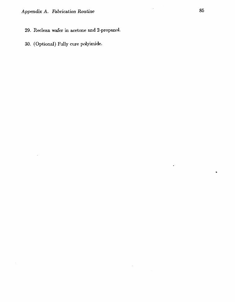
Appendix A. Fabrication Routine
29. Reclean wafer in acetone and Zpropanol.
30. (Optional) Fully cure polyimide.

Appendix B
Design Calculations
B .1 Epitaxial Layer Thickness
The thickness of the epitaxial layer will determine the amount of charge that will be
produced by ionizing radiation, as well as the capacitance, leakage currents, and time
response of the device. Depending on the doping of the layer, the voltage required to
deplete the epitaxial layer from a reverse biassed Schottky diode, is found by solving
Poisson's equation (in one dimension):
where e, is the permittivity of the semiconductor = c,eo (eI(GaAs) = 12.9)
n(x) is the electron concentration,
p(x) is the hole concentration,
N; is the donor concentration,
N i is the acceptor concentration, and
x is the depth into the epitaxial layer, with the surface being at x = 0.
If the epitaxial layer is to be depleted to a depth, w, then for x < W, N$ is much
greater than the other concentrations. For x > w, there is no field and pn,t = 0. Then
Equation B.25 reduces to:
= 0 for x > w

Appendix B. Design Calculations
Solving this while taking E(x = w) = 0 as a boundary condition, gives:
The potential of the system, tj, is found by integrating again to get (taking tj(x = w) =
0 as a boundary condition):
Thus to deplete to a depth w, a voltage of V = e w 2 is required. The voltage, V,
should include the built-in voltage, hi, resulting from the Schottky junction [19,26,27],
as well as the applied voltage Vapplied.
(B. 30)
The built-in voltage of a Schottky barrier on GaAs varies in a not well understood
manner, depending on the technique used to form the junction, as well as on the
condition of the semiconductor surface and the type of metallization used. A good
discussion on the nature of metal-semiconductor junctions can be found in a book by . Sharma [27], or by Rhoderick [41], as well as in various papers (for example [26,42,43]).
For modelling purposes, hi was taken as 0.8V. Table B.6 gives the depletion depth for
various doping densities, No, and voltages, V. It also contains the maximum electric
field in the depletion region. The breakdown field strength for 1 x 1014 cm-3 material
is % 300 kV/cm, and slightly higher for higher dopings [19].
To maximize the depletion depth, and hence signal, a minimum doping level is
required. For commercially available epitaxial material, this is approximately equal
to ND = 1 x 1014cm-3. Starting from this point, an expected signal charge can be
calculated for various depths and traded off against the voltage required to obtain
depletion.
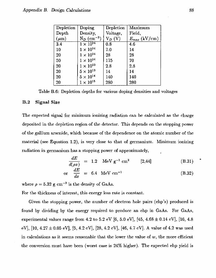
Appendix B. Design Calculations
1 Depletion 1 Voltage,
Depletion Depth (P-4 3.4 10 20 50 20 20 20 20
Maximum Field, Em,, (kV/cm) 4.6 14 28 70 2.8 14 140 280
Doping Density, ND ( ~ m - ~ ) 1 x 10¹⁴ 1 x 10¹⁴ 1 x 10¹⁴ 1 x 10¹⁴ 1 x 10¹³ 5 x 10¹³ 5 x 10¹⁴ 1 x 10¹⁵
Table B.6: Depletion depths for various doping densities and voltages
B.2 Signal Size
The expected signal for minimum ionizing radiation can be calculated as the charge
deposited in the depletion region of the detector. This depends on the stopping power
of the gallium arsenide, which because of the dependence on the atomic number of the
material (see Equation 1.2), is very close to that of germanium. Minimum ionizing
radiation in germanium has a stopping power of approximately,
dE or - = 6.4 MeV cm-'
dx
where p = 5.32 g cmW3 is the density of GaAs.
For the thickness of interest, this energy loss rate is constant.
Given the stopping power, the number of electron hole pairs (ehp's) produced is
found by dividing by the energy required to produce an ehp in GaAs. For GaAs,
experimental values range from 4.2 to 5.2 eV [6, 5.0 eV], [45, 4.68 f 0.14 eV], [16, 4.8
eV], [lo, 4.27 f 0.05 eV], [5, 4.2 eV], [28, 4.2 eV], [46, 4.7 eV]. A value of 4.2 was used
in calculations as it seems reasonable that the lower the value of w, the more efficient
the conversion must have been (worst case is 24% higher). The expected ehp yield is

Appendix B. Design Calculations 89
then approximately 150 per micron. For a 20 micron epitaxial layer this is 3000 ehp's
or 0.48 fC of charge. Note that each ehp contributes only one elementary charge unit
to the total signal, as the electron drifts to one electrode and the hole to the other
resulting in a net transfer across the depletion region of one elementary charge.
B.3 Structure Capacitance
Considering the equivalent circuit of a diode semiconductor detector and the nature of
the signal from such a device (see Chapter 6 and Figure 6.21), the capacitance of the
output node should be calculated to determine the signal size expected. Fof an epitaxial
GaAs layer in full depletion on an S.I. substrate this is equivalent to calculating the
capacity of coplanar electrodes. If it were not for the semi-insulating substrate, or if
the device is not operated in full depletion, the capacitance would be that of a parallel
plate capacitor with a plate separation equal to the depletion depth. Such a device
would.have a capacitance so large that operation on a 20 micron epitaxial layer would
not be possible.
The capacity of coplanar electrodes (see Figure B.52), is calculated by making a
conformal mapping into a region where the electrodes form a parallel plate capacitor.
This is done through two mappings. The first maps the z-plane into the z' = z/a plane
as shown in Figure B.52, and then uses a Schwam-Christoffel to transform the right
half of the z' into the w-plane. This transformation takes the form:
dw -- - A
dz' (2' + b/a)1/2(z' + 1)1/2(z' - 1)1/2(z' - b/a)ll2
Substituting m = alb, and noting
dw - - - dz'
that m < 1 for all strip widths and separations,

Appendix B. Design Calculations 90
Noting that z1 = 1 , l l m are poles in this differential, integration is done separately over
three regions:
On region 1.
where K ( m ) is the elliptic integral of first order.
On region 2.
where K 1 ( m ) is the complementary elliptic integral of first order.
On region 3. R R mAdzl
dw3 = lim R-m ilm (ma,@ - ~ ) l / ~ ( z f l -
take mzl = l / t to get
(B . 36)
(B.37)

Appendix B. Design Cdcula tions 9 1
This maps into the w-plane as shown in Figure B.53. From this an effective parallel
plate configuration with plate width W' and separation Sf can derived, where:
The capacitance per unit length (neglecting fringing effects) of a parallel plate capacitor
Considering that there is both air above the electrodes and semiconductor below, c is
given by:
= (1 + +O
The complementary elliptic integral K1(m) can be written as
K1(m) = K(J~T;;E?)
Then
The actual capacitance seen by the ohmic output is twice this (to account for the
z< 0 plane). The elliptic integrals are implemented in a data manipulation program
called OPDATA [47] which was used to produce Figure B.54 showing the ratio of
for various ratios of W/S.

Appendix B. Design Calculations
z-plane
zl-plane
Figure B.52: Coplanar geometry of Schottky drift electrodes and ohmic output elec- trode. Drift electrode D6, on either side of the ohmic electrode, is the nearest electrode to the output electrode. It is taken together with the other drift electrodes as extending to m.
Figure B.53: Coplanar plates conformally mapped into parallel plates.

Appendix B. Design Calculations
Capacitance o f Coplanar Plates (dimensionless) f o r various Plate W i d t h (W) to Separation
Figure B.54: Capacitance of coplanar plates.

Appendix B. Design Calculations
C (fringing) (pF/cm) 1.74 2.00 2.46 2.64 2.90 3.40 4.16 4.79
Table B.7: Capacitance of coplanar plates with and without fringing fields.
Table B.7 gives calculated capacitances for various W/S ratios. From Table B.7 it is
apparent that a simple parallel plate approximation is not very good and that fringing
fields should be included. The effect of fringing fields is given by:
S' r e W' Cf = Co [I + =In (T)] [48, pp. 1245-124'71
where Co is the capacitance without fringing fields.
Values of Cf for various W/S ratios are also given in Table B.7. On the TPGD the
ohmic output contact has a total length of 2.3 mm and an expected capacitance of 0.61
pF, as the ohmic contact width to separation ratio is 213.
B.4 Response Time
The response time of the detector is determined by the length of time it takes to drift
the signal charge from the point of incidence to the ohmic output contact. This time
is given by the collection time:
where
I is the path taken for the initial point, i to the output ohmic contact, f , and

Appendix B. Design Calculations
vd is the drift velocity (a function of the electric field).
The path will be approximated by path perpendicular to the surface and one parallel
to the surface along the electron potential minimum near the substratelepi interface.
For both sections, the drift velocity is taken as being 1 x lo7 cm/s. This approximation
is valid for the depletion fields expected in 1 x l O I 4 material and for a drift field of 1.33
kV/cm (4 volts between drift electrodes). The maximum drift length is 200 pm in the
TPGD giving a maximum collection time of z 2 ns. This is the time required to collect
all electrons produced by ionizing radiation once the electric field re-establishes itself.
The holes will begin to arrive immediately after production at the Schottky electrodes,
and continue to arrive for 2 ns (assuming a saturation velocity of 1 x lo6 cm/s). The
hole signal will be ca~acitively coupled to the ohmic output contact, resulting in a
pulse with a rise time of 2 ns (although the electrons will arrive with a spread of B 0.22
ns, the total risetime will be governed by the velocity of the holes). The shape of the
rising slope will depend on where the particle strikes the pixel. As the rise times of the
amplifiers used with the TPGD are greater than the pulse rise time, its shape could not
be observed. For a description of pulses shapes, see reference [ll, Chapter3, Section 21 .
B.5 Noise Sources
The noise from three sources was calculated and the sources compared.
B.5.1 Johnson noise
Johnson noise depends on the capacitance of the device in that this capacitance forms a
filtering circuit with resistances in the circuit. Considering an idealized leaky capacitor
detector as in Figure 6.21, the Johnson noise can be found by integrating:

Appendix B. Design Calculations 96
over all frequencies. When convolved with the low pass filter that the detector can be
represented as,
- 2kT Rdw -1 71- 1+w2C2R2 dx
- kT - - C
In terms of equivalent charge, the Johnson noise is given by:
B.5.2 Dark Current
The dark current (reverse leakage current through a p-n junction) is-given by:
where n,;,,, is the minority carrier density, given by n,;,,, = n;2/nmajOr. Hence Jdark =
9.5 x 10-l6 A/cm2 = 0.95 fA/cm2.
B.5.3 Generation Current
The generation current (current produced by thermally generated electrons and holes)
is given by:

Appendix B. Design Calculations
where, for worst case,
T, = 1 x s,
w = 20pm,
n; = 2 x lo6 cm-3
This is considerably greater than the dark current and the dark current will be ne-
glected.
The equivalent noise charge due to the generation current will be the total generation
rate times the carrier transit time, t , (all generation events are independent).
So for a pixel with dimensions of 2000 pm x 360pm x 20pm;
Hence the noise is essentially entirely Johnson noise. Noise due to surface leakage
currents can not be calculated, but is generally larger than any other noise source.
The signal produced by the passage of minimum ionizing radiation through 20 pm
of GaAs is 3000 ehp giving a calculated signal-to-noise of 9 if all the charge is collected
at one output contact and none is lost to traps or recombination centers. With transit
times < 2 ns, trapping may on may not be a problem (minority carrier lifetime is
> 10 ns).

Appendix B. Design Calculations
B.6 Straggling
When a particle passing through a media deposits energy, it is assumed to do so through
a series of random events [I], in each of which the particle loses an average energy of
SE. As the collisions are random the number of collisions per unit path length follows a
Poisson distribution with a standard deviation of dm. Hence the energy deposited
per unit length also follows a Poisson distribution. Integrating over the entire path
length through the media then results in a variation in the energy deposited given by
the square root of the average energy loss.
B.7 Pion Energy Deposition
Pions with a momentum of 292 MeV/c (kinetic energy of 180 MeV) are minimum
ionizing [44] and will have a stopping power of 6.8 MeV/cm. Thus they will lose
14 keV of energy passing through the 20 pm epitaxial layer. Protons with the same
momentum (kinetic energy of 43.1 MeV) are not minimum ionizing and have a stopping
power of 50.54 MeV/cm [44]. At this rate they will lose 101 keV in the epitaxial layer
of the TPGD.

Bibliography
[I] R.D. Evans. The Atomic Nucleus. McGraw-Hill Book Company, Toronto, 1955.
[2] Glenn F. Knoll. Radiation Detection and Measurement. John Wiley & Sons,
Toronto, 1979.
[3] E. Sakai. Present status of room temperature semiconductor detectors. Nuclear
Instruments and Methods, 196(1):121-130, 1982.
[4] G.A. Armantrout, S.P. Swierkovski, J.W. Shersham, and J.H. Yee. What can be
expected from high-Z semiconductor detection? IEEE Transactions on Nuc lear
Science, NS-24(1):121, 1977.
[5] G. Bertolini, F. Cappellani, and G. Restelli. Current state of the art in semicon-
ductor detectors. Nuclear Instruments and Methods, 112:219-228, 1973. . [6] R. Zuleeg and K. Lehovec. Radiation effects in GaAs junction field effect transis-
tors. IEEE Transactions on Nuclear Science, NS-27(5):1343-1354, 1980.
[7] Mayrant Simons. Radiation effects in GaAs integrated circuits: A comparison
with silicon. GaAs I C Symposium, page 124, 1983.
[8] Victor A.J. van Lint. The physics of radiation damage in particle detectors. Nu-
clear Instruments and Methods, A253:453-459, 1987.
[9] K.Hesse, W.Gramann, and D.Hoppner. Room temperature GaAs gamma detector.
Nuclear Instruments and Methods, 101:39-42, 1972.

Bibliography 100
[lo] J.E. Eberhardt, R.D. Ryan, and A.J. Tavendale. Evaluation of epitaxial n-GaAs
for nuclear radiation detector. Nuclear Instruments and Methods, 94:463476,
1971.
[ll] G. Bertolini and A. Coche, editors. Semiconductor Detectors. John Wiley & Sons,
Inc., New York, 1968.
[12] F.B. McLean and T.R. Oldham. Charge funneling in n- and p-type Si substrates.
IEEE Transactions on Nuclear Science, NS-29(6):2018-2023, 1982.
[13] R.M. Gilbert G.K. Ovrebo and J. Schifano. Plasma screening of funnel fields.
IEEE Transactions on Nuclear Science, NS-32(6):4098-4103, 1985.
[14] Micheal Shur, Kang Lee, Robert Choe, and Erik Berger. Charge collection by
drift during single particle upset. IEEE Transactions on Nuclear Science, NS-
33(5):1140-1146, 1986.
[15] R.N. Hall. Recombination processes in semiconductors. Proceedings of the IEE
(London), BlO6(Suppl. 17):923-931, March 1960.
[I61 M.A. Hopkins and J.R. Srour. Measurements of alpha-particle-induced charge in
GaAs devices. IEEE Transactions on Nuclear Science, NS-30(6):4457-4463, 1983.
[17] Frank Stern. Calculated spectral dependence of gain in excited GaAs. Journal of
Applied Physics, 47(12):5382-5386, December 1976.
[I81 R. Boltz (Cominco), January 1987. Private communication.
[19] S.M. Sze. Physics of Semiconductor Devices. John Wiley & Sons, Toronto, second
edition, 1981.

Bibliography 101
[20] Z. Shanfield, M.M. Moriwaki, W.M. Digby, and J.R. Srour. Characteristics of SEU
current transients and collected charge in GaAs and Si devices. IEEE Transactions
on Nuclear Science, NS-32(6):4104-4109, 1985.
[21] Emilio Gatti and Pavel Rehak. Semiconductor drift chamber - an application of
a novel charge transport scheme. Nuclear Instruments and Methods, 225:608-614,
1984.
[22] Emilio Gatti, Pavel Rehak, and Jack T. Walton. Silicon drift chambers - first
results and optimum processing of signals. Nuclear Instruments and Methods,
226:129-141, 1984.
[23] Pavel Rehak, Emilio Gatti, Antonio Longoni, J. Kemmer, Peter Holl, Robert
Klanner, Gerhard Lutz, and Andrew Wylie. Semiconductor drift chambers for
position and energy measurements. Nuclear Instruments and Methods, A235:224-
234, 1985.
[24] J. Kemmer, G. Lutz, E. Belau, U. Prechtel, and W. Welser. Low capacity drift
diode. Nuclear Instruments and Methods, A253:378-381, 1987.
[25] Ira Deyhimy, Richard C. Eden, and Jr. James S. Harris. GaAs and related het-
erojunction charge-coupled devices. IEEE Transactions on Electron Devices, ED-
27(6):1172-1180, 1980.
[26] E.H. Rhoderick. Metal-semiconductor contacts. IEE Proceedings, 129(1):1-14,
February 1982. Part 1.
[27] B.L. Sharma, editor. Metal-Semiconductor Schottky Barrier Junctions and Their
Applications. Plenum Press, New York, N.Y., 1984.

Bibliography 102
[28] Marc Cuzin. Some new developments in the field of high atomic number materials.
Nuclear Ins t rumen t s and Methods, A253:407-417, 1987.
[29] David G. Webster. Detector design considerations. TRIUMF design note, October
1986.
[30] Corrie Kost and Fred Jones. RELAX3D: a FORTRAN program to solve the 3
dimensional Poisson (Laplace) equation. Technical report, TRIUMF Computing
Services, 4004 Wesbrook Mall, Vancouver, B.C., V6T 2A3, February 1987.
[31] Maurice LeNoble. Granular Metal Schottky Gal l ium Arsenide Charge Coupled
Devices. PhD thesis, University of British Columbia, 1988. In process.
[32] Greg R. Smith. The STAR online data acquisition system. Technical report,
TRIUMF, 4004 Wesbrook Mall, Vancouver, B.C., V6T 2A3, July 1987.
[33] XELOSS. A program to calculate energy losses of particles in various materials
using an iterative method.
b
[34] U. Littmark and J.F. Ziegler. Handbook of Range Distributions for Energetic
Ions in A l l Elements, volume 6 of T h e Stopping and Ranges of Ions in Matter.
Pergamon Press, New York, 1980.
[35] Ortec. Ins truments for Research Catalog 1002. EG&G Ortec, 100 Midland Road,
Oak Ridge, Tennessee, 1970.
[36] C.R. Gruhn. A thin epitaxial silicon detector with internal amplification. I E E E
Transactions o n Nuclear Science, NS-23(1):145-152, 1976.
[37] M.A. Hopkins and J.R. Srour. Charge collection measurements on GaAs devices
fabricated on semi-insulating substrates. I E E E fiansactions o n Nuclear Science,

Bibliography
[38] Ronald S. Wagner, Jeffrey M. Bradley, Nicole Bordes, Carl J. Maggiore, Dipen N.
Sinha, and Robert B. Hammond. Transient measurements of ultrafast charge
collection in semiconductor diodes. IEEE Transactions on Nuclear Science, NS-
34(6):1240-1245, 1987.
[39] John N. Bradford. Nonequilibrium effects in VLSI. IEEE Transactions on Nuclear
Science, NS-25(5):1144-1145, 1978.
[40] E. L. Mathie, editor. TRIUMF Users Handbook. TRIUMF, Vancouver, B.C.,
Canada, 1987.
[41] E. H. Rhoderick. Metal-Semiconductor Contacts. Clarendon Press, Oxford, 1978.
[42] John Bardeen. Surface states and rectification at a metal semi-conductor contact.
Physical Review, 71(10):717, 1947.
[43] V.L. Rideout. A review of the theory and technology for ohmic-contacts to group
111-V compound semiconductors. Solid-State Electronics, 18:541-550, 1975.
[44] L. G. Greeniaus. TRIUMF Kinematics Handbook. TRIUMF, Vancouver, B. C.,
Canada, second edition, September 1987.
[45] C.J. Wu and D. B. Wittry. Investigation of minority-carrier diffusion lengths
by electron bombardment of Schottky barriers. Journal of Applied Physics,
49(5):2827-2836, 1978.
[46] P.A. Tove. Review of semiconductor detectors for nuclear radiation. Sensors and
Actuators, 5:103-117, 1984.

Bibliography 104
[47] Phil Bennett and Corrie Kost. Opdata user's guide. Technical Report TRI-CD-
87-04 Ver. 2.9, TRIUMF, 4004 Wesbrook Mall, Vancouver, B.C., V6T 2A3, July
1987.
[48] Philip M. Morse and Herman Feshbach. Methods of Theoretical Physics. McGraw-
Hill Book Company, Inc., Toronto, 1953. Part 11.