incorporated an introduction to spreading resistance analysis … · · 2005-08-31an introduction...
TRANSCRIPT

An Introduction to Spreading Resistance Analysis
and its Application in the Semiconductor Industry
Sheila LoftisDan Dickey
Solecon Labs770 Trademark DrReno, NV 89521(775) 853-5900
www.solecon.com
Cover SOLECON LABS, Reno, Nevada (775) 853-5900
N A SOLECO LABS SEMIN
ARnn
n
p
n
n
n
nnn
n
ppp
SOLECONINCORPORATED
LABORATORIES

SOLECON LABS, Reno, Nevada (775) 853-5900
N A SOLECO LABS SEMIN
AR
FillingSRAR1
SPREADING RESISTANCE ANALYSIS REQUEST FORM
Date Company Engineer
Priority: High o Normal o(surcharge)
Mailing Address(Mail Stop too, please)
Tel #
Purchase Order # Message #(please!)
Fax #
Number of Samples _______________ Total Number of Profiles _______________ email
Sample #Approximate structure expected from surface down:
Type Depth Type Depth Type Depth Type Depth
MaximumDepth ofInterest
CircleSubstrate
Type
CircleCrystal
Orientation
P N <111> <100>
P N <111> <100>
P N <111> <100>
P N <111> <100>
P N <111> <100>
P N <111> <100>
P N <111> <100>
P N <111> <100>
Hard copy carrier concentration plots are supplied automatically. Also available are…Hard Copy: o Resistivity Plot, o Resistance Plot, o Data TableSoft Copy: o Text File(s), o Image File(s) -via:- o 3½" DOS, o E-mail
Reference Job # (if any):
Special Instructions: (Any specific region of the profile of greater importance than the rest?)
If device wafer, please indicate locations required by a sketch below or by attaching a photo or drawing .
Sketch:

FillingSRAR2 SOLECON LABS, Reno, Nevada (775) 853-5900
N A SOLECO LABS SEMIN
AR
1. Solecon Labs privacy policy.
2. Provide us with as much information as possible.
3. An appropriate bevel angle is needed.
4. Solecon strives for over 20 data points per layer.
5. A shallow emitter at .2µm on base at .4µm on epi/buried layer at 5.5µm on p-type substrate. What are you really interested in?
Filling out our request form:

Shallow Profile of the Bipolar Structure
ISOLATION
BA
ES
MTT
R
EI
E
MTT
R
EI
E
EPIEPI
BUR EDIAYER
L
Bipolar1 SOLECON LABS, Reno, Nevada (775) 853-5900
N A SOLECO LABS SEMIN
AR

Deep Profile of the Bipolar Structure
ISOLATION
N- EPI
P substrate
N+ BURIED LAYERN+ BURIED LAYERBASEI
TEM
ERTI TEM
ERT
P+ IS
OLA
TION
Bipolar2 SOLECON LABS, Reno, Nevada (775) 853-5900
N A SOLECO LABS SEMIN
AR

Bipolar3 SOLECON LABS, Reno, Nevada (775) 853-5900
N A SOLECO LABS SEMIN
AR
-3C
arr
ier
Co
nce
ntr
atio
n in
cm
-3C
arr
ier
Co
nce
ntr
atio
n in
cm
DEPTHDEPTH-- micronsmicrons
1010 2020
1010
1010 1818
1010 1717
1010 1616
1010 1515
1010 1414
nn
nn
nn
nn
pppp
pp
nn
nn
nnnnnnnnnnnn
nnnnnnnnnnnn
nn
nn
nn
nn
nn
nn
nn
nnnnnnnnnnnnnn
nnnnnnnnnnnnnnnnnnnnnnnnnnnnnnnnnnnnnnnnnnnn
nnnnnnnnnnnnnnnnnnnnnnnn
nnnnnnnnnnnnnnnnnnnnnnnnnnnn
nn
nn
nn
PP
PPPPPPPPPPPPPPPPPPPPPP
PPPP
00 11 22 33 44 55 66
1919
00 .2.2 .4.4 .6.6 .8.8 11 1.21.2
-3C
arr
ier
Co
nce
ntr
atio
n in
cm
-3C
arr
ier
Co
nce
ntr
atio
n in
cm
DEPTHDEPTH-- micronsmicrons
1010 2020
1010
1010 1818
1010 1717
1010 1616
1010 1515
1010 1414
1919
SS
SSSS
nnnnnnnnnnnnnnnnnn
nnnn
nn
nn
nn
nn
pp
pp
pppppppppppppppppppppppp
pp
nnnnnnnnnnnnnnnnnnnnnnnnnnnnnnnnnn
nnnnnnnnnnnnnnnnnnnnnnnn
nnnnnnnnnnnnnnnnnnnnnnnnnnnnnnnnnnnnnnnnnnnn
nnnnnnnnnnnnnnnnnnnnnn
Bipolar TransistorBipolar Transistor

Sizes SOLECON LABS, Reno, Nevada (775) 853-5900
N A SOLECO LABS SEMIN
ARHow much of the sample do we need?
1. We measure from full wafers to a millimeter square.
2. Pattern wafers and backups.
Size of pattern:
1. Our minimum requirements are 20µm wide x 100µm long.
2. The smaller the pattern size the greater the compromise.
3. For this reason we suggest dedicated spreading resistance test patterns which are 50 x 500µm.
Beveling:
1. Your samples are mounted on angled beveling blocks.
2. Samples should be beveled immediately before probing, to avoid interference from native oxide.

DedTPs SOLECON LABS, Reno, Nevada (775) 853-5900
N A SOLECO LABS SEMIN
AR
Dedicated SRA Test Patterns

Schematic diagram of a spreading resistancemeasurement on a beveled sample
SOLECON LABS, Reno, Nevada (775) 853-5900Bevel
N A SOLECO LABS SEMIN
AR
ie
Dop ng Typ I
iDop ng Type II
eSampl
U
A
METALL
RGI
L
C
JUNCTIO
N
Osmium or Tungsten Carbide Probes

Carrier Type DeterminationWith a Few Modifications, the Spreading Resistance
Set-Up Can Determine “N” or “P”.
ie
Dop ng Typ I
iDop ng Type II
eSampl
One probe is heated.
Polarity and magnitude of the open circuit (Seebeck) voltage determined
U
A
METALL
RGI
L
C
JUNCTIO
N
HotProbe SOLECON LABS, Reno, Nevada (775) 853-5900
N A SOLECO LABS SEMIN
AR

Optical SOLECON LABS, Reno, Nevada (775) 853-5900
N A SOLECO LABS SEMIN
AR
Optical Profilometer view of a spreading resistancemeasurement on a beveled sample

BirdsEye SOLECON LABS, Reno, Nevada (775) 853-5900
N A SOLECO LABS SEMIN
AR
Birds Eye View of SRA Sample and Probes

Probing SOLECON LABS, Reno, Nevada (775) 853-5900
N A SOLECO LABS SEMIN
AR
1. 2 probe tips made of tungsten carbide are used.
2. The probe tips are shaped so that they can be positioned within 20um of each other.
3. Each probe tip is mounted on the end of a separate arm.
4. Each arm pivots on a kinematic bearing system that eliminates lateral motion or "scrubbing" as it contacts the sample.
5. Probe tips are lowered gently onto the sample.
6. Because of the small contact area, pressure is in excess of a million pounds per square inch.
7. 5 millivolts are applied across the probes and the resistance is measured.
Probing

LINEAR CURRENT FLOW
SPREADING RESISTANCE
rLR =
rR =
2rp
2a
La
rwhere is the bulk resistivity in ohm-cm.
rL
LINEAR CURRENT FLOW
SPREADING RESISTANCE
rLR =
rR =
2rp
2a
La
rwhere is the bulk resistivity in ohm-cm.
rL
LINEAR CURRENT FLOW
SPREADING RESISTANCE
rLR =
rR =
2rp
2a
La
rwhere is the bulk resistivity in ohm-cm.
rL
Linear SOLECON LABS, Reno, Nevada (775) 853-5900
N A SOLECO LABS SEMIN
AR

Two Probes on a Thin Layer (t<a):
D. H. Dickey, NBS SP 400-48
aaa
s
t
r lnR =
spt a
ThinLayer SOLECON LABS, Reno, Nevada (775) 853-5900
N A SOLECO LABS SEMIN
AR

Conductivity SOLECON LABS, Reno, Nevada (775) 853-5900
N A SOLECO LABS SEMIN
AR
pe pqnq mmr
s +==1
eqnN
mr
1@@
What is the significance of resistivity? In a semiconductorit is related to the concentration of electrons and holes:
And from that, the dopant concentration can be approximated.

.001 .01 0.1 1 10
n<100>
Resistivity (ohm-cm)
.0001 1000100
p<111>
n<111>
p<100>
1
10
210
310
410
510
610
710
Me
asu
red
Re
sis
tan
ce (o
hm
s)
N A SOLECO LABS SEMIN
AR
Calibration ChartSpreading Resistance
vs. Resistivity (NIST Traceable Si Bulk Standards)
CalibCurves1 SOLECON LABS, Reno, Nevada (775) 853-5900

CalibCurves2 SOLECON LABS, Reno, Nevada (775) 853-5900
N A SOLECO LABS SEMIN
AR
.001 .01 0.1 1 10
Resistivity (ohm-cm)
.0001 1000100
1
10
210
310
410
510
610
710
Me
asu
red
Re
sis
tan
ce (o
hm
s)
n<111>n<100>
n<111>n<100>
n<111>n<100>
2.5g
10g
20g
.001 .01 0.1 1 10
Resistivity (ohm-cm)
.0001 1000100
p<111>p<100>
1
10
210
310
410
510
610
710
Me
asu
red
Re
sist
an
ce (o
hm
s)
p<111>p<100>
p<111>p<100>
2.5g
10g
20g
Calibration Data for Three Probe Loads

Probe Spacing Experiment on Relatively Thin Layers(Measured resistance is dominated by the lateral current flow)
After: Dickey, NBS SP 400-48 p16
01 10 100
Probe Spacing - microns
Me
asu
red
Re
sis
tan
ce
1000
100
200
300
400
500
600W
Sample #1284ohms/sq
Sample #2126ohms/sq
Sample #356.4ohms/sq
aa
s
t
r lnR =
spt a
Spacing SOLECON LABS, Reno, Nevada (775) 853-5900
N A SOLECO LABS SEMIN
AR
10
10
10
10
10
10
10
10
1
2
3
4
5
6
7
8
.
Bevel EdgeM
ea
sure
d R
esi
sta
nce
in O
hm
s
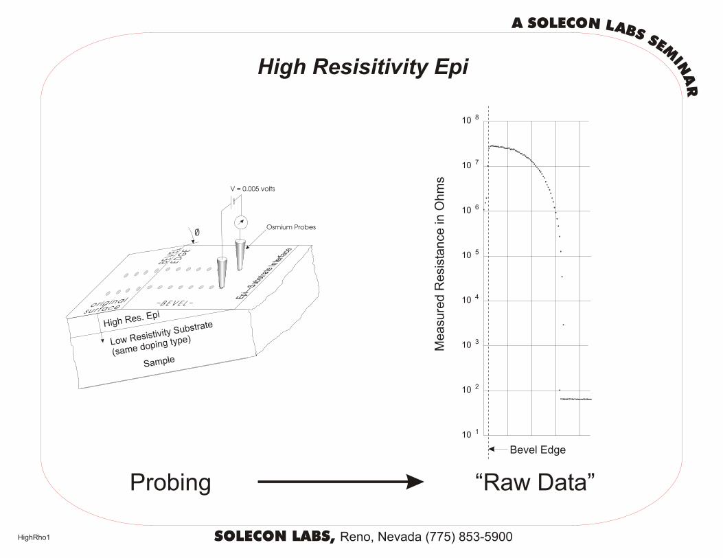
Probing “Raw Data”
High Resisitivity Epi
Hi es pigh R . E
w si ity ub
Lo Re stiv S trates
( ame d g typs
opin)e
Sample
Epi—Sub
strate
Inter
face
HighRho1 SOLECON LABS, Reno, Nevada (775) 853-5900
N A SOLECO LABS SEMIN
AR

High Resisitivity Epi (continued)
“Raw Data” Resistivity Plot
DataReduction
Re
sist
ivity
(o
hm
-cm
)
10
10
10
10
10
10
10
-2
-1
0
1
2
3
4
nnnnnnnnnnnnnnnnnnnnnnnnnnnnnnnnnnnnnnnnnnnnnnnnnnnnnnnn
n
n
n
n
n
NNNNNNNNNNNNNNNNNNNNNNNNN
DEPTH - microns
0 10 20 30 40 50 6010
10
10
10
10
10
10
10
1
2
3
4
5
6
7
8
.
Bevel Edge
Me
asu
red
Re
sist
an
ce in
Oh
ms
HighRho2 SOLECON LABS, Reno, Nevada (775) 853-5900
N A SOLECO LABS SEMIN
AR

High Resisitivity Epi (continued)
Resistivity Carrier Concentration
Carrier Concentration
Calculated Using
Published Carrier
Mobility Values
Re
sist
ivity
(o
hm
-cm
)
10
10
10
10
10
10
10
-2
-1
0
1
2
3
4
nnnnnnnnnnnnnnnnnnnnnnnnnnnnnnnnnnnnnnnnnnnnnnnnnnnnnnnn
n
n
n
n
n
NNNNNNNNNNNNNNNNNNNNNNNNN
DEPTH - microns
0 10 20 30 40
Ca
rrie
r C
on
cen
tra
tion
(c
m)
-3
1010
1010
DEPTH - microns
00 1010 2020 3030 4040
1010
1010
1010
1010
1010
1010
1111
1212
1313
1414
1515
1616
1717
1818
nnnnnnnnnnnnnnnnnnnnnnnnnnnnnnnnnnnnnnnnnnnnnnnnnn
nnnnnnnnnnnnnnnnnnnn
nnnnnnnnnnnnnnnnnnnnnnnnnnnnnnnnnnnnnnnnnn
nn
nn
nn
nn
nn
NNNNNNNNNNNNNNNNNNNNNNNNNNNNNNNNNNNNNNNNNNNNNNNNNN
-3
HighRho3 SOLECON LABS, Reno, Nevada (775) 853-5900
N A SOLECO LABS SEMIN
AR

Correction SOLECON LABS, Reno, Nevada (775) 853-5900
N A SOLECO LABS SEMIN
ARSampling Volume Correction
Our correction algorithms account for the sampling volume on non-uniformly doped layers. In regions with slight to noresistivity gradient, the algorithms tend to magnify the mechanical noise. But without correction the graded layer’s values
can be very wrong! We have various levels of smoothing which we can use to reduce the scatter in your profiles.
Both layers corrected(Unsmoothed data)
Uncorrected layers(Unsmoothed data)
Top layer corrected and smoothed(Uncorrected/unsmoothed substrate)
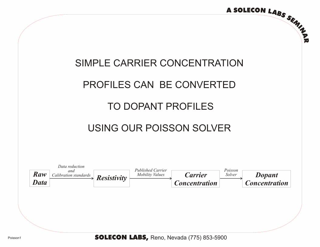
SIMPLE CARRIER CONCENTRATION
PROFILES CAN BE CONVERTED
TO DOPANT PROFILES
USING OUR POISSON SOLVER
RawData
DopantConcentration
Data reductionand
Calibration standardsPublished Carrier
Mobility ValuesPoissonSolver
Resistivity CarrierConcentration
Poisson1 SOLECON LABS, Reno, Nevada (775) 853-5900
N A SOLECO LABS SEMIN
AR

Simple Carrier Concentration Profiles Can Easily Be Converted to Dopant Profiles using Our Poisson Solver
Poisson Solver
Concentration Profile
3 4 5 6210
1410
1510
1610
1710
1310
CarrierConcentration
-3(cm )
Dopant Profile
DEPTH — microns3 4 5 6210
1410
1310
1510
1610
1710
DopantConcentration
-3(cm )
Poisson2 SOLECON LABS, Reno, Nevada (775) 853-5900
N A SOLECO LABS SEMIN
AR

.
70 keV 1e15, 4e15,1e16 10B into Silicon (circa 1983)
From : James Ehrstein et al, ASTM Special Technical Publication 850, D. C. Gupta, editor, p. 415.
SIMS Typically Reports Greater Depth in the Tail Region of B Diffusions.In the Following Example, Boron was Implanted into Single-crystal Si.
SRA
SIMS
DEPTH — microns
-3C
on
cen
tra
tion
(cm
)
(not ours)
Sims SOLECON LABS, Reno, Nevada (775) 853-5900
N A SOLECO LABS SEMIN
AR

11 MeV Arsenic Implant
“The implantations were carried out using the facilities of the Lawrence Berkeley Laboratory. 11 MeV beams were obtained from a dynamatron with a 2.2 megavolt terminal. The ion source is a conducting crystal of gallium arsenide from which arsenic ions in the 5+ charge state were sputtered and extracted into the accelerator column.”
From Megavolt Arsenic Implantation into Silicon, a paper presented at the 1982 International Conference on Metallurgical Coatings and Process Technology by P.F. Byrne, N. W. Cheung, and D.K. Sadana, University of California, Berkeley.
Many thanks to Peter Byrne for permission to reproduce and disseminate this very impressive profile.
nn
nn
nn nn
nn
PPPP
0 1 2 3 4 5
1410
1510
1610
1710
1810
1910
6
DEPTH — microns
As11MeV SOLECON LABS, Reno, Nevada (775) 853-5900
N A SOLECO LABS SEMIN
AR

nn nn n n
n
n
n
n
nnnnnnn
nnnnnn
n
n
n
n
n
pppppp pp
pppppppppppppppp
pppppppp
PPPPPPPPPPPPPPPPP
n
0
1410
1510
1610
1710
1810
1910
2010
4 8 12 16 20 24
CarrierConcentration
-3(cm )
DEPTH — microns
P-TYPE CONTAMINATION— PROBABLY FROM BORONCONTAMINATED ANTIMONY
P-CONTAMINATION
EPI
N+BURIEDLAYER
(Antimony)
BContamination SOLECON LABS, Reno, Nevada (775) 853-5900
N A SOLECO LABS SEMIN
AR

2010
1910
1810
1710
1610
1510
1410
0 4 8 12 16 20 24
CarrierConcentration
-3(cm )
DEPTH — microns
nnnnnnnn nnnnnnnn
nn
nnnn
nn
nn
nn
nnnn
nn
nn
PPPP PP
SRP Through a Buried Layer Pattern:SRP Through a Buried Layer Pattern:
nnnnnn nnnn nn
nn nn
nn
nn
nnnn
PP PP
2010
2010
1910
1910
1810
1810
1710
1710
1610
1610
1510
1510
1410
1410
00 44 88 1212 1616 2020 2424
CarrierConcentration
-3(cm )
CarrierConcentration
(cm )-3
DEPTH — micronsDEPTH — microns
SRP through the Field:SRP through the Field:
AutoDoping SOLECON LABS, Reno, Nevada (775) 853-5900
N A SOLECO LABS SEMIN
AR
Arsenic Autodoping During Epitaxial Deposition
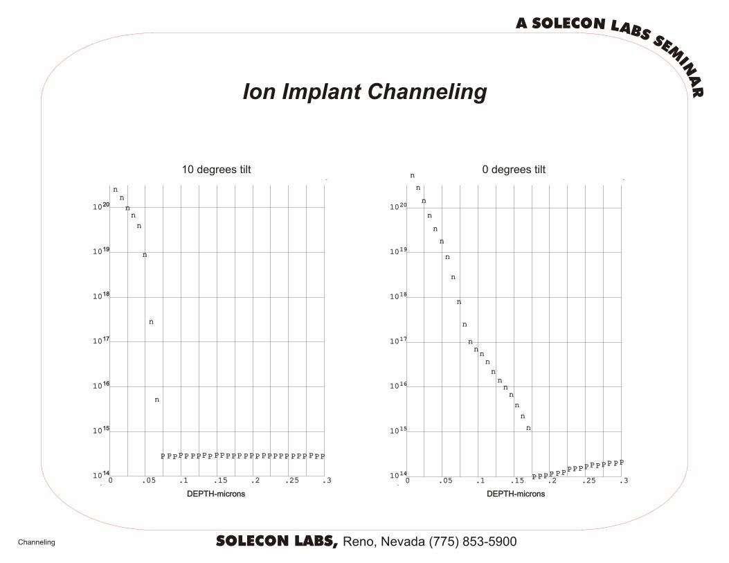
Ion Implant Channeling
Channeling SOLECON LABS, Reno, Nevada (775) 853-5900
DEPTH-micronsDEPTH-microns
..
..
1010
1010
1010
1010
1010
1010
1010
1414
1515
1616
1717
1818
1919
2020
nn
nn
nn
nn
nn
nn
nn
nn
nn
nn
nnnnnnnnnnnnnnnn
nn
nn
nn
PPPPPPPP PPPPPPPP
PPPPPPPPPPPP PPPP
00 .05.05 .1.1 .15.15 .2.2 .25.25 .3.3..
..
1010
1010
1010
1010
1010
1010
1010
1414
1515
1616
1717
1818
1919
2020
nnnn
nnnn
nn
nn
nn
nn
PP PPPPPPPP PPPPPPPP PPPPPPPPPP PPPPPP PPPPPPPPPP PPPPPP PPPPPP
00 .05.05 .1.1 .15.15 .2.2 .25.25 .3.3
DEPTH-micronsDEPTH-microns
0 degrees tilt10 degrees tilt
N A SOLECO LABS SEMIN
AR

P+ Isolation Diffusion into N-Epi
pppppppppppppppppppppppp
pp pp
pp
2010
1910
1810
1710
1610
1510
1410
0 4 8 12 16 20 24
CarrierConcentration
-3(cm )
DEPTH — microns
ADEQUATEISOLATION
Wafer A
PPPPPPPPPPPPPPPPPPPPPPPPPPPPPPPPPPPPPPPPPPPPPPPPPPPPPPPPPPPPPPPPPPPPPPPPPPPPPPPPPP
pp
pp
pppp
pppppppppppppppppppppppppppppppppppp
pppppppppppppppppppp
pppppppp
pppppppppppppppppppppp
pppppppppppp
pppppppppppppppppppppp pppp pppp
2010
1910
1810
1710
1610
1510
1410
0 4 8 12 16 20 24
CarrierConcentration
-3(cm )
DEPTH — microns
PRECARIOUS!
A VERY MARGINALISOLATION
Wafer B
P+Iso SOLECON LABS, Reno, Nevada (775) 853-5900
N A SOLECO LABS SEMIN
AR

Thermal Donors — A Severe Case
p
p
pp
p
p
ppppppppppppp
ppp
pppp
p
pp
p
PPPPPPPP
PPPP
PPP
P PPPP
PP
PPPPpp
pPp Pppp
pppppp
pp
pppppp
ppppppp
pppp
pppp
ppppp
p
pppppppppp
ppp
p
pppp
p
ppp
p
p
ppp
pp
DE P T H - m i c ro n s
10110 .5 1.0 1.5 2.0 2.5 3.0
10
10
10
10
10
13
14
15
16
17
1012
3 -C
arr
ier
Co
nce
ntr
atio
n (c
m)
bulk dopingof wafer~ 2e14p-type
OxyDoners SOLECON LABS, Reno, Nevada (775) 853-5900
N A SOLECO LABS SEMIN
AR
Inactive SOLECON LABS, Reno, Nevada (775) 853-5900
N A SOLECO LABS SEMIN
AR
DEPTH - microns
0.1 0.2 0.3 0.4 0.5 0.6
10
10
10
10
10
10
10
7
6
5
4
3
2
1
2M
ob
ility
(cm
/ V
-se
c)
nn
nn
nnnnnnnnnnnnnnnnnnnn
nnnnnnnnnnnnnnnnnnnnnnnnnnnnnnnnnnnnnnnnnnnnnnnnnnnnnnnnnnnnnnnnnnnnnnnnnnnnnnnnnnnnnnnnnnnnnnnnnnnnnnnnnnnn
nnnnnnnnnnnnnnnnnnnnnnnnnnnnnnnnnnnnnnnnnnnnnnnn
0
Me
asu
red
Re
sist
an
ce (
Oh
ms)
••
••
••••••••••••••
••••••••••••••••••••••••••••••••••••••••••••••••••••••••••••
••••••••••••••••••••••••••••••••••••••••••
••••••••••••••••••••••••
••••••••••••••••••
••••••
DEPTH - microns
0.1 0.2 0.3 0.4 0.5 0.6
10
10
10
10
10
10
10
20
19
18
17
16
15
14
0
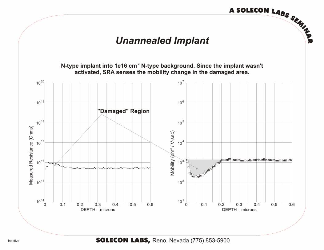
"Damaged" Region
Unannealed Implant
-3N-type implant into 1e16 cm N-type background. Since the implant wasn'tactivated, SRA senses the mobility change in the damaged area.

CMOS SOLECON LABS, Reno, Nevada (775) 853-5900
N A SOLECO LABS SEMIN
AR
DEPTHDEPTH-- micronsmicrons
pp
pp
nnnnnnnnnnnnnnnnnnnnnnnnnnnnnnnnnnnnnnnn
nnnnnnnnnn
nn
nn
nn
pp
pp
pppppppppppppppppppp
pppppp
pp
pppppppppppp
pppppppppppppppp
pppppppppppppp
pppppppppppppppppppppppppppppppppppppppppppppppppppppppppppppp
ppppppppppppppppppppppppPPPPPPpp
pp
pp
nnnnnnnnnnnnnnnnnnnnnnnnnnnnnnnnnnnnnnnn
nnnnnnnnnn
nn
nn
nn
pp
pp
pppppppp
pppppppppppp
pppppppppppppppppp
pppppppp
1010
1010
1010
1010
1010
1010
1010
1010
1313
1414
1515
1616
1717
1818
1919
2020pppppppppppp
pppppppppppppppppp
pp
pp
pp
pp
pp
nnnnnnnn
nnnnnnnnnnnn
nnnnnnnnnnnnnnnn
nnnnnn
DEPTHDEPTH-- micronsmicronsDEPTHDEPTH-- micronsmicrons
00 22 44 66 88 1010 121200 11 22 33 44 55 6600 .1.1 .2.2 .3.3 .4.4
Shallow Profile toCharacterize the Source-Drain
Steeper Profile (Plotted on 2 Depth Scales)to Characterize the
N-Well, Epi, and Substrate
CMOS (P-channel Source-Drain)

Factors SOLECON LABS, Reno, Nevada (775) 853-5900
N A SOLECO LABS SEMIN
AR
Factors influencing SRP measurements(X , Shape, Carrier Concentration)j
1) Bevel edge: Clear edge is required to identify fringes from different films near the active area, starting points and footprints. We use high quality optical microscope with dark field illumination to identify this
2) Bevel angle: Bevel angle multiplied by step increments influence the depth. Can influence shape, X , Base width measurements, etc. j
particularly in shallow SRPs
3) Step increments
4) Location of interest: Falling out of pattern and probing adjacent structures can lead to distorted profiles
5) Probe tip condition: Probe penetration, Calibration, Data Smoothing: While smoothing data, it is necessary to follow data trends, visually examine and suppress concavity or convexity and not allow data to follow random noise by choosing best fits and appropriate correction factors

Structures SOLECON LABS, Reno, Nevada (775) 853-5900
N A SOLECO LABS SEMIN
ARCommon Structures of Interest For SRA
CMOS STRUCTURES
• Epi/Substrate
• P-Well/Epi
• N-Well/Epi
• Poly/Gate Ox/Epi
• Poly/Gate Ox/N-Channel
• Poly/Gate Ox/P-Channel
• P+/Epi
• P+/NWell
• N+/Epi
• N+/PWell
• NLDD
• PLDD
• Under field Ox with implant
• Under field Ox without implant
BIPOLAR STRUCTURES
• Epi/Substrate
• Epi/Buried Layer/Substrate
• Base/Epi
• Base/Epi/Buried layer/Sub
• Base/Isolation/Epi/Sub
• Emitter/Base/Epi
• Emitter/Base/Epi/Buried layer
• Sinker/Epi/Sub
• Sinker/Epi/Buried layer
• Isolation/Epi/Sub

QAChecklist SOLECON LABS, Reno, Nevada (775) 853-5900
N A SOLECO LABS SEMIN
ARQA Checklist
1. Was the profile run in the location specified by the requester?2. Were the final profiles shown to lab supervisor?3. Are the profiles plotted with correct crystal orientation?4. Was the customer contacted for information regarding orientation or a break
test done?5. Are the step increments optimal?6. Do the job numbers match those of customer copy?7. Do the sample numbers match those of customer copy?8. Are there different profiles for the same file numbers and sample numbers?9. Are the file numbers matching with customer copy?10. Was Calibration Check done for epi samples?11. Are the correction factors, smoothing factors optimal?12. Was hot probe done on all samples where this was necessary? Hot probes
wires not reversed?13. Do scalings (y axis) match so customer can overlay with reference jobs and
supreme 4?14. Has frsp been tried for p to p+ and n to n+ layers and for dips at epi to n+
junctions?15. Were the bevel angle scales chosen on the full axis according to information
posted at profilometer?16. Was there a close correlation between the 4 point probe and SRA data sheet rho
on bare silicon/test samples?17. Check customer satisfaction to see if profiles are in line with his expectations.

Qmetrics SOLECON LABS, Reno, Nevada (775) 853-5900
N A SOLECO LABS SEMIN
AR
Quality Systems In Line With ISO 9001/17025
• Management responsibility• Quality manual• Business planning• Contract review• Written procedures on critical operations• Purchasing• Control of customer supplied samples• Sample identification and traceability via job tracking system• Statistical techniques• Measurement and inspections• Control of measurement and test equipment• Control of non conforming profiles• Corrective and preventive actions• ESD control• Internal and external quality control audits• Control of quality records• Customer training records• Shipping of profiles• Customer satisfaction records• Inter lab comparisons, round robin records

WhySRA SOLECON LABS, Reno, Nevada (775) 853-5900
N A SOLECO LABS SEMIN
AR
1. Over 25 years of experience and continuous improvement in the art and science of beveling and probing with best known method on profiling carrier concentration.
2. High spatial resolution of dopant and depth profiles.
3. Low cost operation and high return on investment for customers, easily affordable.
4. Turnover within 24 hours available.
5. Fast and accurate feedback to fab and foundries.
6. Over 300 satisfied customers.
7. Both SRA and process expertise available at Solecon Labs.
8. Edge over competitors as far as reproducibility goes.
Why Solecon Labs and SRA