incremental analysis of large vlsi layouts
TRANSCRIPT

ARTICLE IN PRESS
INTEGRATION, the VLSI journal 42 (2009) 203–216
Contents lists available at ScienceDirect
INTEGRATION, the VLSI journal
0167-92
doi:10.1
$ A p
connect
Design
the con
conside� Corr
E-m
prosenj
journal homepage: www.elsevier.com/locate/vlsi
Incremental analysis of large VLSI Layouts$
Akash Agrawal a, Prosenjit Gupta b,�
a International Institute of Information Technology, Hyderabad, Indiab Mentor Graphics, Hyderabad 500082, India
a r t i c l e i n f o
Article history:
Received 17 October 2007
Received in revised form
26 May 2008
Accepted 25 June 2008
PACS:
85.40.�e
85.40.Bh
Keywords:
Layout verification
Design rule checking
Connectivity and device extraction
Incremental algorithm
External memory algorithm
60/$ - see front matter & 2008 Elsevier B.V. A
016/j.vlsi.2008.06.005
reliminary version of this paper appears a
ivity extraction for large VLSI layouts, in: Pr
and Test Symposium, 2007, pp. 259–267 [1]. T
ference paper. Moreover, DRC and device
red in the conference paper at all, are covere
esponding author.
ail addresses: [email protected]
[email protected] (P. Gupta).
a b s t r a c t
The verification of VLSI layouts is an important and expensive step in physical design process and has
significant contribution in overall design cycle time. Design rule checking, connectivity extraction and
device extraction are important steps in layout analysis. Efficient incremental algorithms for these steps
are crucial for fast development as well as small time-to-market of the design. If the size of layout is so
large that it cannot fit entirely into available main memory, the main performance bottleneck is
communication between internal memory and the external memory due to the slow access speed of
external memory.
In this paper, incremental solutions for problems of layout analysis are presented considering the
external memory management. The main component of these algorithms is the proposed ‘‘recursive
tiling’’ approach, which provides an easy to implement data structure for the aggregation of parts of
layout for fast search and updates. Experimental results show that the recursive tiling approach
proposed in this paper has reduced the time required for incremental processing on the workstations
with limited amount of physical memory.
& 2008 Elsevier B.V. All rights reserved.
1. Introduction
Integrated circuit artwork depicts a circuit layout as acollection of polygons on different layers called masks. The aimof physical design verification step is to verify the functional anddesign rule correctness of the layout representation of circuit. It isgenerally divided into several sub-stages and normally starts withlayout analysis which involve design rule checking (DRC),connectivity extraction, device extraction, etc. The layout ischecked to ensure the desired functionality of circuit representedby layout, and proper fabrication.
The design and fabrication technology imposes several con-straints on geometry and relative positions of the layout features.These are called design rules and the process of checking theserules is called design rule checking (DRC). After checking the layoutfor design rules and removing the violations, functionality of thelayout is verified by circuit extraction phase. It takes the layout as
ll rights reserved.
s ‘‘A. Agrawal, Incremental
oceedings of 11th IEEE VLSI
his is an expanded version of
extraction, which are not
d here.
(A. Agrawal),
input and extracts the connectivity in the form of netlist byidentifying the transistors and the interconnections (nets).
The complexity of current generation VLSI systems and theiterative nature of design process require design changes toincorporate, typically late at one or more levels of the designprocess. Late design changes are made in order to correct logicaland/or technological problems in the circuit. The design of high-performance circuits requires iterations of the design flow tocorrect mistakes made earlier or accommodate changes madelater in the flow. Traditionally, layouts are verified from scratchafter every modification irrespective of the size of update. Thetime needed for layout analysis of entire VLSI layout is quite large,even when hierarchical methods are used. For every layoutmodification, hours of verification run on a mainframe computeris very common at the final stages of chip assembly. This is acritical phase of the design schedule because, when the layout isnearly complete, it is difficult to coordinate simultaneous work byseveral designers. Incremental techniques can achieve greatsavings by limiting layout analysis to only those portions oflayouts that have actually changed since the last verification run.Therefore, algorithms and data structures are needed which canfacilitate efficient search and update of layout parts that are beingmodified or optimized. The algorithms should also be able to givethe results of new modifications considering the previouslycompiled result, in short amount of time. This requires veryefficient incremental algorithms and data structures.

ARTICLE IN PRESS
A. Agrawal, P. Gupta / INTEGRATION, the VLSI journal 42 (2009) 203–216204
Moreover, algorithms and data structures present in literatureare designed assuming that there is a large amount of memoryavailable and any memory location can be accessed with same(constant) cost. The assumption of infinite main memory (MM) isnot true in practical machines. The memory hierarchy of acomputer system can be divided into a number of levels, witheach level differing in its cost and performance characteristics. Intypical computer systems, the lowest level CPU registers andcaches are used with the fastest but expensive memory anddynamic random access memories (DRAM) are used for internalMM. In the higher level, inexpensive but slower magnetic disksare used for external mass storage. These days in many large-scaleapplications, including those of VLSI layout editing, the data to bemanipulated reside at different levels of memory due to limitedamount of available MM. As the access speed of external memory(EM) is a million times slower than that of the internal memory,the main performance bottleneck in computation for theseapplications is the input/output transfer (or simply I/O) betweenlevels of memory instead of the internal processing time. One canuse standard MM algorithms and data structures for processingbut the performance can be far below the optimal. To process suchlarge amounts of data we need algorithms and data structuresthat can reduce the amount of data access from the EM. Thesealgorithms and data structures are called external memory (EM)algorithms and data structures.
For incremental changes in such layouts, secondary memoryhas to be searched for the portions that have to be modified andload those portions into MM from secondary memory. Thisrequires lot of I/O (in terms of MM block) between MM and EM.Due to the slow access speed of EM, the time required to load thelayout is much larger than the time required to process the layout.Hence, efficient EM algorithms and data structures are required tofacilitate incremental updates in verification of large VLSI layouts.
1.1. Previous work
Layout analysis (DRC and circuit extraction) is a well-studiedproblem in terms of MM algorithms [2–6,35–37]. The algorithmsfor layout analysis differ in many ways such as use of structuralinformation present in layouts, constraints imposed on thegeometry of mask features, internal data representation scheme,etc. Baker [2] presented an algorithm for transistor extraction thatuses a raster based approach for internal representation andoperations on the layout. Seiler [7] proposed an approach toimplement raster based design rule checker in hardware toimprove the speed of processing.
Another popular data representation scheme is the cornerstitched [8] representation. Magic’s layout editor system uses thisdata structure for DRC [6] and circuit extraction [5]. Anotherpopular approach to process layout geometries is the scan lineapproach. In this approach a scan line [9] is moved from top tobottom (or left to right) on a layout of a chip, pausing at thevertices of the geometry (see [4,10–12]).
The polygon based circuit extraction algorithms either dividethe polygons into trapezoids or use bounding rectangles for scanline geometry, because of the complexity of polygonal operations[3,13–16]. Design rules can be easily mapped to some sequence ofpolygon geometric operations such as expansion, intersection,enclosure, etc. The algorithms for DRC, that use polygons as scanline object, use these polygon geometric operations to check thedesign rules [17,18]. A common method to locate short circuit inVLSI circuit is to construct a connectivity graph of the shorted netsand find a shortest path between the nets. The required memoryis proportional to the size of nets and may be quite large. A spaceefficient algorithm for finding short circuits in layouts is proposedby Su et al. [19].
Although a lot of work has been done in MM algorithms foranalysis of VLSI layouts, not much work has been done in terms ofI/O efficient data structures and algorithms for the same. Due toincreasing size and complexity of present day VLSI layouts, I/Oefficient data structures and algorithms are needed to reduce thetime to process current generation VLSI layouts and hence, toreduce the design cycle time. Some work has been done in therecent past in EM algorithms for layout analysis [20]. An EMalgorithm for DRC is proposed by Ganesh et al. [21], whichpartitions the layout in fixed tiles using the tiling approach [22]and uses the polygon-algebra based operations to process eachtile. Another EM algorithm for connectivity extraction using thetiling approach is given by Sharathkumar et al. [23], which usesscanline approach to process each tile. These algorithms are goodfor offline processing, but the disadvantage is that they do notsupport updates. An EM algorithm for validation of large VLSIcircuits is presented in [24].
1.2. Our contribution
In this paper, we have proposed an EM data structure calledrecursive tiling to support efficient incremental updates in largeVLSI layouts. This mechanism divides the layout into smaller tiles(subproblems) which can be independently solved using aminimum number of I/Os. It is a generalization of the tilingapproach [22] extended to incremental setting. This division of alarger problem into smaller and independent subproblems alsoproves to be useful for large layouts that may fit into MM. Therecursive tiling approach is presented in Section 3.
Using the recursive tiling data structure, we have proposed EMalgorithms for the incremental layout analysis (DRC, connectivityextraction and device extraction) problem for large VLSI layouts.For simplicity, we have assumed that a layout is represented as aset of rectilinear polygons on different layers such that no twopolygons on the same layer intersect. In the rest of this paper weuse polygons to refer to rectilinear polygons for simplicity. Asthese polygons can be partitioned into a set of non-overlappingrectangles in one scan, we further assume that the layoutpolygons are given as set of rectangles. The set of rectangles thusobtained from a polygon is called the cover of the polygon and theunion of the rectangles is the polygon itself. We use the scan lineapproach to process each tile.
In the rest of the paper we look at the problems of layout analysisin the context of large VLSI layouts and develop EM solutions tothem. The EM model used to study the algorithms is given in Section2.1. The analysis of VLSI layouts is divided into three parts: DRC,connectivity extraction and device extraction. We first address theproblem of DRC in Section 4. Sections 5 and 6 address the problem ofconnectivity extraction and device extraction, respectively.
2. Preliminaries
2.1. EM model
The most widely used memory model for input/outputcomplexity (I/O-complexity) analysis of EM algorithms is givenby Aggarwal and Vitter [25]. The model has the followingparameters:
N ¼ number of elements in problem instance;M ¼ number of elements that can fit into the MM;B ¼ number of elements that can fit into one MM block,
where MoN and 1pBpM=2.

ARTICLE IN PRESS
A. Agrawal, P. Gupta / INTEGRATION, the VLSI journal 42 (2009) 203–216 205
In this model, the CPU processes the data available in MM. An I/Ooperation in this model is defined as the swap of a block of B dataitems of MM with the consecutive B data items of the EM. The I/Ocomplexity of the algorithm is defined simply as the number of I/Ooperations performed. For example, the I/O complexity of readingall the input data is N=B. As the time for internal computation ismuch smaller than the time required for I/O communication, CPU isidle for most of the time. Therefore, for the asymptotic analysis ofEM algorithms internal computation time is ignored.
The quotients N=B (number of blocks in the problem) and M=B
(number of blocks that can fit into MM) are normally used inanalysis of EM algorithms and are denoted as n and m,respectively. Sorting, permutation and scanning are well-studiedproblems in EM [25–27]. The I/O complexity for these standardalgorithms can be represented as
scanðNÞ ¼ OðN=BÞ ¼ OðnÞ
sortðNÞ ¼ OððN=BÞlogM=BðN=BÞÞ ¼ Oðn logm nÞ
permðNÞ ¼ OðminðsortðNÞ;NÞÞ
In the rest of the paper we have used EM and MM to representexternal memory and main memory respectively.
3. Recursive tiling: an EM data structure
The incremental changes are done on the layout to improve theperformance or for error correction. These changes are generallylocal and affect only a small portion of the layout. Due to localnature of most of the updates, existing algorithms can be easilymodified to perform incremental layout analysis. The maindifficulty in incremental processing is to find the portions of layoutthat have to be updated. Therefore, a mechanism is required thatcan facilitate efficient search of the portions of layout that are beingmodified. Existing algorithms of layout analysis can then be appliedon these portions to get the result of updates.
The approaches used for searching the portions of layoutdepend on the representation and the data structure used to storethe layout. Although many tree based approaches can be extendedto EM settings [27–29], implementing tree based approacheseffectively can be difficult. Moreover, the trees are optimal in I/Osonly when updates are processed in batch mode, a requirementthat can be satisfied but is constraining to the designer.
A partitioning technique called tiling was proposed bySharathkumar et al. [22]. The proposed partitioning methoddivides the layout area into fixed tiles based on the square root law[9]. But, in case of incremental updates, the number of componentsðNÞ keeps changing and hence, the tiling done on the basis of initialN may not be balanced after some cycles of updates. Contents andhence, the size of some tiles may be larger than the others. To getthe result of the updates, we process the tiles in which updates aredone. So the I/Os required to process these tiles may not bebounded in the incremental setting. One approach to avoid this isto perform tiling again on the complete layout after significantamount of modifications. But this necessitates the scan andredistribution of polygons in those tiles also which are unaffectedby the updates and hence, makes unnecessary I/Os. Generalexperience shows that the load time of layouts are more than theactual processing time and hence scanning of entire layout must beavoided to get a practically useful incremental scheme.
3.1. Recursive tiling
Here we present a dynamic tiling scheme called recursive tiling,which is a generalization of the tiling approach of [22]. In this
approach, each tile is defined by the memory size and not by thegeometric object’s position in the layout. It keeps track of sizes ofthe tiles (i.e. the amount of information stored in tiles) and dividesa tile into smaller ones if its size grows beyond the maximum tilesize (in terms of MM blocks), defined later. It merges smaller tilesinto a bigger one if the tiles are small enough such that theircombined size is comparable to other tiles. Since recursive tilingapproach ensures that the memory size of each tile is bounded ateach stage, it is useful in incremental settings.
Most of the MM algorithms use ‘‘sort-and-scan’’ technique toprocess the layout. The maximum size of tile can be found withthe help of following two points:
(1)
Sorting the data in small chunks takes lesser time than sortingthe complete data (as in bucket sort [30]).(2)
Once the disk starts transferring the data, it can transfer atvery high speed. Initialization of data transfer from a disktakes more time than the afterward transfer of data.Dividing the layout into small tiles can boost the processing timeof large layouts. But more number of tiles can cause an increase inI/O time. Through experiments we have seen that there is anoptimal tile size below which the time for I/O dominates thesorting time and above which sorting time dominates the I/Otime. This is dependent on the hardware and it is different foreach hardware configuration. This optimal tile size can be taken asthe maximum size above which tiles get divided into smaller tiles.
3.2. Algorithm
We first divide the layout area intoffiffiffiffiffiffiffiffiffiffiffiN=M
phorizontal andffiffiffiffiffiffiffiffiffiffiffi
N=Mp
vertical equispaced partitions using the square root law[9], and distribute the polygons. All polygons that intersect a tile isstored in that tile. A polygon P intersects a tile T if one of thefollowing conditions is true:
(1)
if the polygon is completely enclosed by a tile boundary, (2) if a tile is completely enclosed by the polygon, (3) if any of the vertices of polygon is inside the tile boundary, (4) if any of the polygon edge intersects the tile boundary.We divide each tile into smaller tiles of maximum allowed size(optimal size). If the size of any tile exceeds the maximumallowed size of the tile (in terms of MM blocks), we furtherrecursively partition that tile into smaller tiles of maximumallowed size in a similar fashion. An example of recursive tiling isshown in Fig. 1.
To perform the recursive tiling and to access the content oftiles we need to maintain an index structure to keep track ofnumber of polygons in each tile and the sub-tiles generated. Weuse a tiling tree for this indexing purpose which is an instance ofBþ tree [31]. Each leaf node of the tree represents one tile and theroot of the tree represents the complete layout. The intermediatenodes represent big tiles which are divided into smaller ones. Theleaf nodes represent the tiles that cannot be further divided. Thetiling tree of Fig. 1 is shown in Fig. 2.
In Fig. 1, the size of tile number 00, 32 and 44 exceeds thedefined maximum size of tile, hence, these tiles are divided intosmaller tiles and children of corresponding node in tiling tree arecreated as shown in Fig. 2.
Each node of the tiling tree contains a count of the number ofpolygons stored in the corresponding tile (root for completelayout, intermediate nodes for bigger tiles and leaf nodes forsmaller tiles). When layout is updated, we update the polygoncount of tiling tree nodes corresponding to updated tiles. If, due to

ARTICLE IN PRESS
4
0
3
2
1
0
2 31 4
Fig. 1. Recursive tiling of a given layout. Tile 00, 32 and 44 are further divided into
smaller tiles and children of corresponding node in tiling tree are created as shown
in Fig. 2.
00 01 02 11 22
Complete Layout
42 44
Fig. 2. Tiling tree of Fig. 1. Children of nodes 00, 32 and 44 are created because
corresponding tile is divided into smaller tiles (as shown in Fig. 1).
A. Agrawal, P. Gupta / INTEGRATION, the VLSI journal 42 (2009) 203–216206
the insertion operation, the total size of polygons (in terms on MMblocks) stored in a tile exceeds maximum defined size of tile, wedivide the tile into smaller ones and children are created for thecorresponding node in tiling tree. If, due to deletion operation, thenumber of polygons in any intermediate node of tree drops belowminimum size, we merge the tiles corresponding to the childrenof this node and delete the children. We assign this node the newtile formed due to merging.
3.3. Analysis
Size of each tile is fixed at small constant number of MM blocksto minimize the I/Os required for update. As the size of each tile isbounded by constant number of memory blocks, i.e. OðBÞ blocks, tostore complete layout with N polygons, we need OðN=BÞ leaf nodes.Since each node contains only a constant amount of information(such as polygon count, pointer to tile, children pointers etc.), thememory required to store the tree is small. For example, let
the maximum size of tile ðin terms of mainmemory blocksÞ ¼ S,MM block size is ¼ 4 KB,size of layout is ¼ 64 GB,the number of nodes required to store thecomplete tree ¼ 64 GB
S�4 KB ¼16 M
S ,for constant node size, the space required to storecomplete tree ¼ K�16 MB
S ,
where K is a constant, which depends on amount of informationstored in a node. So the space complexity for the tiling tree is
OðN=BÞ, where N is the number of input polygons and B is thenumber of the polygons that can fit into one MM block.
In an incremental setting, to process the updates we load onlythose tiles from EM to internal memory which get affected due toupdates and process them sequentially. As the size of a tile is onlya small number of MM blocks, the memory required to process atile is only a small fraction of the available MM. Hence, most of theinternal memory is left free. As the memory required to store thetiling tree is small even for large layouts (shown above), we canalways keep the tiling tree in MM so that searching for a tile andupdates in the tiling tree are internal memory operations and donot require any I/O.
3.4. Advantages
The recursive tiling data structure is easy to implement andmaintain. Since the sizes of the tiles are small, the total processingtime for the layout using such tiles is lesser than that using largertiles. This is due to the fact that sorting the data in small chunkstake lesser time than sorting the complete data at once. Thisrecursive tiling approach not only provides reduction in I/O waittime but also can help in reducing the CPU time, so that even if thelayout can fit entirely into available MM, the recursive tiling canbe used to improve in processing time.
The recursive tiling data structure also provides an efficientmechanism for the extension of MM application to EM because,any existing MM algorithm for layout processing can be used toprocess the tiles. This recursive tiling approach can be used inmany other incremental algorithms such as point location,segment intersection, etc., which are basic components in manyalgorithms including those in VLSI physical design automation.
The recursive tiling data structure can also be used to facilitatedistributed processing of layouts. Once the layout is partitioned,tiles can be processed independently on different machines. Afterall the tiles are processed, the results can be combined easily. Theactual mechanism of partitioning and merging for distributedsetting depends on the specific problem.
4. EM incremental DRC
For flat designs, the VLSI layout can be viewed as disjoint setsof polygons on different layers called masks. The technology usedto manufacture integrated circuits imposes certain constraints onthe size and relative position of device features in layout, whichare called design rules.
The goal of incremental design rule checking (DRC) is to reportthe violations of design rules due to incremental updates, i.e.insertion or deletion of polygons in layout. The result of theseupdates can be either violation of design rules in the layout orcorrection of the previous violation. More formally, the online DRCcan be defined as follows: ‘‘Preprocess the given layout such thaton insertion or deletion of a polygon in the layout, the changes indesign rule violations due to these updates can be reportedefficiently’’. A dynamic or incremental algorithm, which checks fordesign rules in presence of insertions and deletions, is very usefulfor layout editors.
In this paper we have considered the set of design rules givenby Mead and Conway [32] which are specified in terms of ascalable parameter l. We consider the general set of rules forCMOS technology as example. For simplicity of illustration weassume that CMOS process involves only four different layerswhich are metal, polysilicon, diffusion and contact (or via) and theset of rules are minimum width rule, minimum separation rule,minimum overlap rule and minimum enclosure rule. The rules

ARTICLE IN PRESS
w w
Fig. 4. (a) Partial expansion of the partition P of the rectangle R by width w. (b)
Partial shrinkage of the partition P of the rectangle R by width w.
Overlapped Area
Fig. 5. Intersection of two rectangles. Here hatched region shows the overlapping
part of the two rectangles.
A. Agrawal, P. Gupta / INTEGRATION, the VLSI journal 42 (2009) 203–216 207
and the checker can be extended to work with any number oflayers.
4.1. Primitive functions
A formal approach for DRC is given by Modarres et al. in [17].This approach divides the problem of checking design rules as aset of simple primitive functions, whose combination is used tocheck the design rules. In this section we review the set ofprimitive functions required to check the design rules given byMead and Conway.
4.1.1. Partition
A partition P of a rectangle R can be defined as interval of anedge of R, coordinates of which are subsets of coordinates of thatedge, as shown in Fig. 3. In the figure hgh; cd; ef ; abi is a partition ofsimple rectangle hei; ad; ei; adi.
4.1.2. Expansion and shrinkage
The expansion function EðR;wÞ is defined as EðR;wÞ ¼ R0 ¼
hxmin �w; ymin �w; xmax þw; ymax þwi, where R ¼ hxmin; ymin;
xmax; ymaxi is the rectangle to be expanded by w. Similarly theshrinkage function SðR;wÞ is also defined.
Generally partition of edges of rectangles are involved in theDRC hence, the partial expansion and partial shrinkage areimportant functions. The partial expansion PEðR;wÞ returns theset of rectangles which represent the expanded partition ofrectangle R by w. Similarly, the partial shrinkage function PSðR;wÞ
is defined.For example, let a partition of horizontal edge ei is
gh ¼ hxmin; y; xmax; yi, the partial expansion and partial shrinkageof this partition by w can be given as hxmin; y; xmax; yþwi andhxmin �w; y�w; xmax þw; yi. The partial expansion and shrinkageis shown in Figs. 4 (a) and (b), respectively.
4.1.3. Intersect
The intersect function returns a rectangle R which is theintersection of two rectangles. Given two rectangles R1 and R2, ifthey intersect, the intersect function returns a rectangle R, whichis R1 \ R2, i.e. the common area in both, else it returns f. Theintersect function is shown in Fig. 5.
4.1.4. Cover
In some design rules like minimum overlap, we need to find,whether the set of partially expanded rectangles is covered by agiven rectangle or not. This cover function returns True if the givenrectangle covers the set of rectangles. Otherwise it returns False.
d
cb
a
fe g h i
Fig. 3. Partition of a simple rectangle R. Here hgh; cd; ef ; abi is a partition of the
simple rectangle hei; ad; ei; adi.
4.1.5. Area
The function area AreaðRÞ is defined as AreaðRÞ ¼ ðxmax � xminÞ�
ðymax � yminÞ, where R ¼ hxmin; ymin; xmax; ymaxi is the rectanglewhose area has to be computed.
4.2. Our solution
In this section we present an algorithm for the incrementalDRC which uses the EM management using the recursive tilingapproach mentioned in Section 3. Solution to the problem ofincremental DRC can be divided into two phases, the preproces-sing phase and the update phase. The update phase consists ofinsertion and deletion of polygons in any of the four layers of theCMOS process considered. The algorithms for the preprocessingand update phases are given below:
4.2.1. Preprocessing
(1)
Perform the recursive tiling on the given layout as discussedin Section 3. Assign each polygon a unique id. Fragments ofpolygon P are stored in tile T , if polygon P intersects the tile T ,i.e. T \ Paf. Store the number of fragments stored in a tile incorresponding node of tiling tree.(2)
Process each tile in row wise fashion to check violations inconsidered design rules as follows:(a) Sort the contents of tile with lower left x-coordinate ofpolygons as primary key and lower left y-coordinate assecondary.
(b) Minimum width rule:(i) Apply partial shrinkage function, with w ¼
minimum width required, on edges of all the poly-gons.
(ii) Apply cover function on the resulting rectangles tocheck for coverage of the set of rectangles by theoriginal polygons.

ARTICLE IN PRESS
A. Agrawal, P. Gupta / INTEGRATION, the VLSI journal 42 (2009) 203–216208
(iii) If the cover returns TRUE, the rule is satisfied elsestore the polygon id in the violated rule datastructure.
(c) Minimum overlap rule:(i) Apply intersect function on the polygons of poly-
silicon and diffusion layers to find the overlappingpartitions.
(ii) Apply partial expansion function, with w ¼
minimum overlap required, on the edges of theseset of partitions.
(iii) Apply cover function on the resulting rectangles tocheck for the coverage of these set of rectangles byoriginal polygons of polysilicon and diffusion layer.
(iv) If cover function returns TRUE, this rule is satisfiedelse store the responsible polygon id in the violatedrule data structure.
(d) Minimum separation rule:(i) For each layer apply partial expansion on the poly-
gons with w ¼ ðminimum separation requiredðintralayerÞÞ=2.
(ii) For each layer apply intersect function on theseexpanded polygons.
(iii) If the intersect function returns a NULL set, the intralayer minimum separation rule is satisfied else storethe responsible polygon id in the violated rule datastructure.
(iv) Repeat above step with a pair of interacting layers andw¼ðminimum separation requiredðinter layerÞÞ=2 tocheck for inter layer minimum separation rule.
(e) Minimum separation rule (between features of same layerwhich are embedded in features of another layer):
(i) For each layer find the set of polygons of that areenclosed in polygons of other layers.
(ii) Apply partial expansion function on the set ofenclosed polygons with w ¼ ðminimum separationrequiredÞ=2.
(iii) For each layer apply intersect function on theseexpanded polygons.
(iv) If the intersect function returns a NULL set, this rule issatisfied else store the responsible polygon id in theviolated rule data structure.
(f) Minimum enclosure rule:(i) For each layer find the set of polygons of contact layer
which are enclosed in this layer.(ii) Apply partial expansion function on the set of poly-
gons of contact layer with w ¼minimum enclosurerequired.
(iii) Apply cover function to check the coverage of theseset of rectangles by original polygons of the corre-sponding layer.
(iv) If cover function returns TRUE, this rule is satisfiedelse store the responsible polygon id in the violatedrule data structure.
(g) Minimum area rule:(i) Apply the area function on all the rectangles of each
polygons.(ii) Add the area of rectangles to get the area of each
polygon.(iii) If the area of polygon is greater than or equal to the
required minimum area, this rule is satisfied elsestore the responsible polygon id in the violated ruledata structure.
(3)
Minimum feature density rule:(a) For each tile apply area function on all the polygons ofeach layer and add them to get the total area covered byfeatures in that layer.
(b) Divide the area covered by features with the area of tile toget the density of features of a layer in that tile.
(c) Store the feature density of each layer with the tile itselfalong with the information of violation of minimumfeature density rule of a layer.
(d) Compute the average feature density of a layer by addingthe feature densities of that layer in all tiles and dividingby the number of tiles.
(e) If the feature density is less than the minimum densityrequired, report error for the layer. To show the possibleareas to correct the problem tiles with densities less thenminimum density can be reported.
There may be many implementations of violated rule datastructure. One possible implementation is a hash table associatedwith every tile. The key for the hash table can be polygon id andthe data can be the type of error and/or the place of error. Thehash table is stored with the tile. Since the hash table containsonly erroneous polygons which are stored in the correspondingtile, the space required for hash table of each tile is also OðBÞ.Hence, each tile can be processed in Oð1ÞI=O.
Since each tile is accessed only once and the I/O required toprocess each tile is Oð1Þ due to limited size of tile, the I/O requiredfor processing all tiles is OðN=BÞ (or simply OðnÞ). So the I/Ocomplexity of preprocessing step is OðnÞ or scanðNÞ.
4.2.2. Updates
The updates can be either insertion or deletion of polygons inany of the four layers. The algorithm for the update following aninsertion or deletion is as follows:
(1)
Divide the polygons in fragments with the help of partitioninginformation stored in the tiling tree. Associate each fragmentwith the corresponding tile id.(2)
Collect all the tiles that are to be modified by these polygons.Process these tiles sequentially as follows:(a) Adjust the polygon count of the corresponding tiling treenode and its parents till root.(b) Apply intersect function on each layer to find the polygons
to be modified.(c) Minimum width rule:
(i) For edges of all polygons to be modified, apply partial
shrinkage function with w ¼ minimum width re-quired.
(ii) Apply cover function on the resulting rectangles tocheck for the coverage of these set of rectangles bythe original polygons.
(iii) If the cover returns TRUE, this rule is satisfied andhence check the violated rule data structure andremove the polygon id (if present), else store thepolygon id in the violated rule data structure.
(d) Minimum overlap rule:(i) Apply intersect function on the polygons of poly-
silicon and diffusion layer to find the overlappingpartitions. Consider only those partitions that containat least one polygon which has been modified.
(ii) Apply the partial expansion function, with w ¼
minimum overlap required, on edges of these set ofpartitions.
(iii) Apply the cover function on the resulting rectanglesto check for the coverage of these set of rectangles bythe original polygons of polysilicon and diffusionlayers.
(iv) If the cover returns TRUE, this rule is satisfied andhence check the violated rule data structure and

ARTICLE IN PRESS
A. Agrawal, P. Gupta / INTEGRATION, the VLSI journal 42 (2009) 203–216 209
remove the polygon id (if present), else store theresponsible polygon id in the violated rule datastructure.
(e) Minimum separation rule:(i) For each layer apply partial expansion on the modified
polygons with w ¼ minimum separation required(intra layer).
(ii) Apply intersect function on each layer individually onthese expanded polygons.
(iii) If the intersect function returns a NULL set the intralayer minimum separation rule is satisfied. Hencecheck the violated rule data structure and remove thepolygon ids (if present) of modified polygons, elsestore the responsible polygon id in the violated ruledata structure.
(iv) Repeat above steps with a pair of interacting layersand w ¼ minimum separation required (inter layer)to check for inter layer minimum separation rule.
(f) Minimum separation rule (between features of same layerwhich are embedded in features of another layer):
(i) For each layer find the set of original/modifiedpolygons that are enclosed in modified/originalpolygons of other layers.
(ii) Apply partial expansion function on this set ofenclosed polygons with w ¼minimum separationrequired.
(iii) For each layer apply intersect function on theseexpanded polygons.
(iv) If the intersect function returns a NULL set, this rule issatisfied. Hence check the violated rule data structureand remove the polygon ids (if present) of modifiedpolygons, else store the responsible polygon id in theviolated rule data structure.
(g) Minimum enclosure rule:(i) In each layer find the set of original/modified
polygons that enclose the modified/original contactlayer polygons.
(ii) Apply partial expansion function on the set of poly-gons of contact layer with w ¼ minimum enclosurerequired.
(iii) Apply the cover function to check for the coverage ofthese set of rectangles by polygons of the correspond-ing layer.
(iv) If the cover returns TRUE, this rule is satisfied. Hencecheck the violated rule data structure and remove thepolygon id (if present) of modified polygons, elsestore the responsible polygon id in the violated ruledata structure.
(h) Minimum area rule:(i) Apply the area function on all the rectangles of
updated polygons.(ii) Add the area of rectangles to get the area of updated
polygon.(iii) If the area of polygon is greater than or equal to the
required minimum area, this rule is satisfied. Hencecheck the violated rule data structure and remove thepolygon id (if present) of modified polygons, elsestore the responsible polygon id in the violated ruledata structure.
(3)
Minimum density rule:(a) For each updated tiles apply area function on the updatedpolygons of each layer and adjust the total area covered byfeatures in that layer.
(b) Update the feature densities of modified layers in this tileand the rule violation information accordingly. Update theaverage feature densities of layers for complete layout.
(c) If the feature density is less than the minimum densityrequired, report error for the layer. To show the possibleareas to correct the problem tiles with densities less thenminimum density can be reported.
(4)
If update is an insertion in a layout, check the size of updatedtiles. If the size of any tile exceeds the maximum tile size,divide that tile and create children of the corresponding nodein the tiling tree.(5)
If the update is a deletion, check if the size of parent of anyupdated tile is less than the minimum size, merge the childrentiles of that node to create one tile.In the update phase, if insertion or deletion of set of P polygonsaffect K unique tiles, we access only these K tiles resulting in OðKÞ
I/Os. Since the violated rules data base for each tile is associatedwith the tile itself, updating it will not require any additional I/O.Hence the I/O complexity of the update phase is OðKÞ, where K isthe number of tiles to be updated.
One problem with the tiling approach is that, we cannot see oruse the data (mask features) stored in another tile while processingone tile. This may lead to errors in computation. Interactionbetween tiles has to be maintained for the correctness of algorithm.For example, while checking minimum separation rule, the featuresclose to boundary have to be checked with features that are onother side of the boundary for the separation rule otherwise, it maymiss the error. There can be many possible ways to handle thisinteraction. One possible solution is to use the overlapping tile. Eachtile boundary is extended to the right and top by a width W , whichdepends on the design rules like minimum width or minimumseparation rule. But due to overlapping, tiles may cause duplicateprocessing of some polygons. This can be avoided by storing theactual and extended tile boundaries. The polygons starting after theactual tile boundary can be omitted from insertion in the statusqueue of the scan line while processing a tile.
5. EM incremental connectivity extraction
The main goal of incremental connectivity extraction process isto report changes in connectivity information due to insertion ordeletion of polygons in the layout. The change in connectivity dueto update can be an instance of a short or open circuit in thelayout. More formally, online connectivity extraction is defined asfollows: ‘‘Preprocess the given layout such that on insertion ordeletion of a polygon in layout the change in connectivity can bereported efficiently’’. A dynamic or incremental algorithm, whichrequires updating connectivity in presence of insertions anddeletions, is very much useful for layout editors.
Incremental update in connectivity extraction is a considerablyharder problem than in other phases of layout verification like,DRC, device extraction, etc. For example, design rule violations mayoccur only in the limited vicinity of the updates (insertion ordeletion of polygons). However, insertion or deletion of a polygonsmay cause many nets to get connected together or a single netbreak into many. Hence, the connectivity of every device connectedto the original net(s) gets affected. The small changes in a layoutcan have far reaching effect on the circuit connectivity. Changingconnectivity in EM setting (i.e. for layouts that cannot fit entirelyinto available MM) may lead to large number of I/Os, which is veryexpensive because of the slow speed of secondary memory.
5.1. Connectivity model
The electrical connections in layouts are established using themetal and via (or contact) layer polygons. Two polygons of

ARTICLE IN PRESS
A. Agrawal, P. Gupta / INTEGRATION, the VLSI journal 42 (2009) 203–216210
different metal layers are connected through a polygon of via layerin between the two metal layers. In this paper we consider onlytwo metal layers and one via layer in between them. The sameapproach can be extended for more number of metal and vialayers.
The proposed connectivity model, for this work, is as follows[23]: consider the three layers of simple polygons M1 (1st metallayer), VIA (via layer) and M2 (2nd metal layer). No two polygonson the same layer intersect. Intersecting polygons can be mergedduring preprocessing. A polygon m1 of layer M1 is electricallyconnected to polygon m2 of layer M2 if both enclose a polygon v oflayer VIA as shown in Fig. 6. In the layout, two polygons P and Q
are considered to be connected if there is a sequence P ¼
P1P2P3 . . . Pk ¼ Q such that Pi is electrically connected to Piþ1 asshown in Fig. 7. Such sequences are called connected components.Connected components show the actual electrical connectivity inthe layout.
Each design is associated with a net list. Each net can beconsidered as a signal and is associated with a unique net id. Weassume that each polygon is attached with the net id of the net itbelongs to. Now we define the notion of short circuits and opencircuits in the layout. If two polygons, which are originally ondifferent nets, belong to the same connected component, it showsthat the nets are electrically connected. It is an instance of short
circuit and the two nets are said to be shorted. If two polygons,which are originally on the same net, belong to differentconnected components, it shows the break in electrical connec-
Metal 1
Metal 2
Via
Fig. 6. Electrical connection is established between two metal layer polygons if
they both enclose the same via layer polygon.
P
Fig. 7. Rectangle P and Q are electrically connected as ther
tivity of that net. It is an instance of an open circuit and the net issaid to be open.
5.2. Our solution
Now we present an algorithm for online connectivity extrac-tion, which considers the EM management, using the recursivetiling approach described in Section 3. The solution of onlineconnectivity extraction can be divided into two phases; thepreprocessing phase and the update phase. The update phaseconsists of insertion and deletion of polygons in any of the threelayers considered in the connectivity model presented above. Thealgorithms for the preprocessing and update phases are givenbelow:
5.2.1. Preprocessing
(1)
e is a
Perform recursive tiling on the given layout as discussed inSection 3. Assign a unique id to each polygon. A fragment ofpolygon P is stored in a tile T , if polygon P intersects the tile T ,i.e. T \ Paf. Store the number of fragments stored in a tile incorresponding node of tiling tree.
(2)
Process each tile in row wise fashion as follows:(a) Load the tile in MM.(b) Run the MM polygon enclosure algorithm to find outmetal and via polygon enclosure and intersection pairs.(c) Store these pairs in two arrays M1V (for the ðM1;VIAÞ
pairs) and M2V (for the ðM2;VIAÞ pairs).(d) Sort M1V and M2V with metal polygon id as the primary
key. With each pair store the tile id and pair type(intersection or enclosure) also.
path
(3)
Search the two arrays M1V and M2V to form connectedcomponents using the following two facts:(a) If a via polygon is intersected by a metal polygon of somelayer, it cannot be enclosed by any metal polygon of samelayer.
(b) If a via polygon is enclosed by a metal polygon of somelayer, it cannot be enclosed by any other metal polygon ofsame layer.
(4)
For each component perform the following:(a) If all the polygons are of same net id, store the componentin an array of components in a position generated byapplying a hash function on the net id.
(b) If the component contains two or more polygons ofdifferent net ids, report short circuit and store the triplet
Q
from P to Q which is electrically connected.

ARTICLE IN PRESS
A. Agrawal, P. Gupta / INTEGRATION, the VLSI journal 42 (2009) 203–216 211
ðM1;VIA;M2Þ, which create the short in the sort circuit tree
which can be an instance of buffer tree. Store thecomponent with both net ids in the array of componentsby applying hash function on both the net ids.
(c) If the net id is already present in the array, merge both thecomponents. If the resulting components have morethan one part, report open circuit and store that net idin the open circuit tree which can be an instance ofbuffer tree and store the component in the array ofcomponents.
As each tile is accessed only once, the I/O required for processingall tiles is OðN=BÞ, where N in the size of layout and B is the MMblock size in bytes (refer to the memory model in Section 2.1),which can also be written as scanðNÞ. Forming the connectedcomponents requires sort and scan of all enclosure pairs stored inthe arrays M1V and M2V . The I/O required for this, due to the I/Ocomplexity of scanning, is essentially OððN=BÞlogM=BðN=BÞÞ. It canalso be written as sortðNÞ. Therefore the I/O complexity ofpreprocessing step is sortðNÞ.
5.2.2. Update
The updates can be either insertion or deletion of polygons inany of the three layers. The algorithm for insertion and deletion isas follows.
Insertion
(1)
Divide the polygons into fragments using the partitioninginformation stored in the tiling tree. Associate each fragmentwith corresponding tile id.(2)
Collect all the tiles which have to be modified by thesepolygons. For each such tile, perform the following steps:(a) Store fragments in the tile and adjust the polygon count ofcorresponding tiling tree node and its ancestors up theroot.
(b) Run MM algorithm to find connected component pairsformed by all new fragments to be stored in the currenttile.
(c) Apply hash function on the net ids of these pairs to findcomponents to be modified. Modify the componentsaccordingly.
(d) Check the modified components for short circuit andupdate the short circuit tree. Store the components in thearray of components.
(e) If the number of polygons in a particular tile exceeds themaximum tile size, divide the tile and create children ofthe corresponding node in the tiling tree.
Deletion
(1)
Divide the polygons into fragments using the partitioninginformation stored in the tiling tree. Associate each fragmentwith the corresponding tile id.(2)
Collect all the tiles which have to be modified bythese polygons. For each such tile perform the followingsteps:(a) Run the MM algorithm to find connected component pairsformed by all the fragments that are to be deleted fromthis tile.
(b) Apply the hash function on the net ids of these pairs tofind the components in the array of components to bemodified. Modify the components accordingly.
(c) If a component gets divided into two or more parts due tothe deletion of the polygon, store the net id of thatcomponent in the open circuit tree.
(3)
If the size of parent of any tile is less than the minimum size,merge the children tiles of that node to create one tile.In the update phase, if insertion or deletion of set of P polygonsaffect K unique tiles and requires L components to be modified,only K tiles are accessed, resulting in OðKÞ I/Os. Each component tobe modified can be accessed in Oð1Þ I=O with the help of hashfunction. Hence, the update phase has I/O complexity of OðK þ LÞ.
Some nets may cross a tile boundary many times and whileprocessing a tile it may appear as an open circuit. This problem isresolved in Step 4. This step takes care of dividing or merging thenets when they cross the tile boundary. The proposed algorithmmay be extended to distributed processing with slight variation inmaintaining the interaction between tiles. For distributed proces-sing, each client can have its own hash table of connectedcomponents (nets) during the processing phase. After completingprocessing of all the tiles, clients can return their hash table asresult. The results of all the clients are merged to get final result.
6. EM incremental device extraction
The aim of incremental device extraction is to efficiently reportthe changes in the device information due to incremental updatesin layout. An incremental update can be either an insertion or adeletion of a polygon. The resulting change can be formation ofnew transistors, deletion of old transistors or change in properties(like shape, perimeter, etc.) of existing transistors. More formallythe online device extraction is defined as follows: ‘‘Preprocessthe given layout such that on insertion or deletion of a polygon inthe layout, the change in device information can be reportedefficiently’’.
6.1. Our solution
An algorithm for incremental device extraction from large VLSIlayouts is presented in this section. We use ‘‘recursive tiling’’ datastructure, mentioned in Section 3, to handle large layouts andsupport incremental changes. The algorithm for incrementaldevice extraction can be divided in two phases; the preprocessingphase and the update phase. Updates in layout can be eitherinsertion or deletion of polygon(s) in polysilicon and/or diffusionlayers. The algorithms for the preprocessing and update phasesare given below:
6.1.1. Preprocessing
(1)
Perform the recursive tiling on the given layout as discussedin Section 3. Assign each tile a unique id. A fragment ofpolygon P is stored in tile T , if polygon P intersects the tile T ,i.e. T \ Paf. Store the number of fragments stored in a tile inthe corresponding node of tiling tree.(2)
Process each tile in row wise fashion to check for validtransistors (Fig. 8) as follows;(a) Sort the rectangles stored in a tile with lower leftx-coordinate of the rectangle as primary key and lowerleft y-coordinate as secondary.
(b) Compute all the overlapping regions of diffusion andpolysilicon layers. These overlapping regions or commonregions are called ‘‘AND rectangles’’ of diffusion andpolysilicon layers and are defined by the four partialedges from each rectangle as shown in Fig. 10.
(c) Sort and store the list of AND rectangles.(d) Scan the AND rectangles list and form connected
components (polygons) of AND rectangles. Assign a

ARTICLE IN PRESS
TransistorDiffusionPolysilicon
Fig. 8. Transistors is formed by overlap of diffusion and polysilicon layer polygons. A valid transistor is formed if polysilicon polygon separates the diffusion polygon into
two separate regions on either side of polysilicon region. The overlapping region works as channel or gate and the two diffusion regions work as source and drain. Figs. (a)
and (b) represent valid transistors while (c) represents invalid transistor. The encoding style mentioned above for transistors, diffusion and polysilicon materials are used
throughout this chapter.
A. Agrawal, P. Gupta / INTEGRATION, the VLSI journal 42 (2009) 203–216212
unique component id to each connected component andstore in a connected component data structure, which canbe an instance of a hash table stored in each tile, with thecomponent id. Assign the corresponding component id tothe AND rectangle.
(e) If a connected component contains AND rectangle(s)which touches tile boundaries, the connected componentextends in that tile also. Store the tile id along with theconnected component.
(f) Scan all the connected components stored to check forvalid transistors. If an AND polygon has two non-adjacentdiffusion edges, then include it as an instance of atransistor. This is because if an AND polygon has twodiffusion partial edges, then the polysilicon part of theAND polygon divides the corresponding diffusion regioninto two disconnected parts. These two parts can be usedas source and drain of the transistor and the AND regionitself being used as the transistor channel.
(3)
Scan and merge the transistors reported due to connectedcomponents extended in more than one tiles to removeduplicate transistors.As each tile is accessed only once and the I/O required to processeach tile is Oð1Þ due to limited size of tile, the I/O required forprocessing all tiles is Oðn=BÞ which can also be written as scanðnÞ.The scanning and merging of transistors to remove duplicatereporting also requires, in the worst case, Oðn=BÞ I/Os. So the I/Ocomplexity of preprocessing step is Oðn=BÞ.
6.1.2. Update
The updates can be either insertion or deletion of polygons inpolysilicon and/or diffusion layers. The algorithm for insertion anddeletion is as follows:
(1)
Divide the polygons into fragments using the partitioninginformation stored in the tiling tree. Associate each fragmentwith the corresponding tile id.(2)
Collect all the tiles that have to be modified by these polygons.For each such tile perform following operations:(a) Adjust the polygon count of corresponding tiling tree nodeand its ancestors.(b) Find the AND rectangles formed by fragments of updates.(c) Find the component ids of connected components to be
modified by finding the AND rectangles that intersect
with these updated AND rectangles. Modify the compo-nents accordingly.
(d) Scan the modified component to report valid transistors.
(3) If the update is an insertion, check, if the number of polygonsin a particular tile exceeds the maximum size of tile, dividethe tile and create children of the corresponding node in thetiling tree.
(4)
If the update is a deletion, check, if the size of parent of anytile is less than the minimum size, merge the tiles corre-sponding to children of that node to create one tile.In the update phase, if insertion or deletion of a set of P
polygons affect K unique tiles, we access only these K tilesresulting in OðKÞ I/Os. As the transistors are small and canextend, in the worst case, into four tiles (if the rectangle is in thecorner) as shown in Fig. 9, the I/Os complexity of the update phaseis OðKÞ.
The interaction between tiles is resolved by the method used inStep 2e to store components when they cross the tile boundaries.The components which crosses the tile boundaries are mergedand then checked (Step 3) for valid transistors to remove duplicatereporting of transistors or errors generated due to partitioning ofpolygons.
7. Hierarchical layout analysis
Hierarchical layout can be modeled as a rooted directedtree whose leaf nodes represent flat layouts as shown inFig. 11. Each node is associated with a transformation matrixwhich represents a combination of transformations such astranslation by some real number in x or y direction, rotationby an integer multiple of 90� or mirroring about x or y axis.The non-leaf nodes represent the layouts in different level ofhierarchy.
In other words, hierarchical layouts can be formed by acollection of flat layouts. The new layouts can be defined whentraversing the hierarchical layout from bottom up. At any non-leafnode, layout can be formed by transforming all rectangles ofchildren nodes by corresponding transformation matrix andmerging the similar layers to form new layers. Implementa-tion of a module in physical design depends on the constraintsapplied on that module. Instantiations of same module can besubjected to different constraints and hence can have different

ARTICLE IN PRESS
Fig. 9. Figure shows the partitioning of transistors due to tiling. As the size of transistors are small, a transistor can extend into maximum of 4 tiles. Hence, each tile can be
updated in Oð1Þ I=O and the update phase requires OðKÞ I/Os to update K tiles.
D
D D
D
PP
P P
PP
P
PP
P P
P
D
P
PP P
D
P P P
PPP
3 D 4 D
D DP
PP
P P P PP
PP PD
21
Fig. 10. The figure shows the AND rectangles which are overlapping regions from
polysilicon and diffusion layers and the connected component formed by these
AND rectangles are shown in right. Each AND rectangle is defined by its edges.
Patterns (a) and (b) forms valid transistors as they have a pair of non-adjacent
diffusion edges (D). Pattern (c) is invalid transistor, as the AND rectangle 1 has two
diffusion edges (D) adjacent to each other. This means that the corresponding
polysilicon (P) edges could not break the diffusion region into distinct source and
drain regions and hence cannot form a transistor channel.
H, T
H2, T21 H2, T22L4, T23
L1, T11 L2, T12 L3, T13 L1, T11 L3, T13
Fig. 11. The tree representation of the hierarchical structure of layout.
A. Agrawal, P. Gupta / INTEGRATION, the VLSI journal 42 (2009) 203–216 213
implementations in physical design. So the leaf nodes correspond-ing to a module can be different depending on the physicalimplementation of instantiation. Hierarchical layouts can also beanalyzed by recursive tiling approach proposed in this paper. The
steps for hierarchical layout analysis using recursive tilingapproach is as follows:
(1)
Collect all the different leaf nodes, i.e. different implementa-tions of instantiated modules and consider them as indepen-dent layouts.(2)
Apply recursive tiling approach to these independent layouts(layouts corresponding to leaf nodes) and analyze them (DRC,connectivity extraction and device extraction) by the methodproposed in this paper.(3)
To analyze the layouts of higher levels in hierarchy, instantiatethe layouts of children after applying corresponding transfor-mation. Consider each instantiation as one feature andprocess the layout using recursive tiling approach.(4)
The same procedure is followed till root of the tree, i.e. toplevel of hierarchy.As the verification results depend on neighbors, the boundarypolygons of an instantiation have to be checked against thepolygons outside the boundary. To resolve this while processing amodule, boundary polygons of its implementation can be movedoutside the boundary after checking. At the time of instantiationthe inner boundary can be treated as the boundary for theinstantiation so that the boundary polygons are visible outsideand their interaction in layout can be checked.
In the update phase, i.e. on insertion or deletion of a polygon inany module or implementation of a module, we first find themodules and the implementations that have to be updated andprocess those implementations. If the changes are on theboundary polygons of implementation we go to the higher levelof hierarchy for verification otherwise stop the verification here.
ARTICLE IN PRESS
A. Agrawal, P. Gupta / INTEGRATION, the VLSI journal 42 (2009) 203–216214
To process the higher levels of hierarchy we transform thechanges with the help of transformation matrix into higher levelsand use the same method for verification.
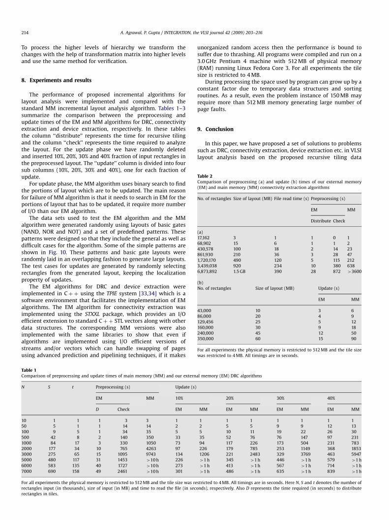
Table 2Comparison of preprocessing (a) and update (b) times of our external memory
(EM) and main memory (MM) connectivity extraction algorithms
No. of rectangles Size of layout (MB) File read time (s) Preprocessing (s)
EM MM
Distribute Check
(a)
17,162 3 1 1 0 1
68,902 15 6 1 1 2
430,578 100 18 2 14 23
861,930 210 36 3 28 47
1,720,170 490 120 5 115 212
3,439,038 920 234 10 380 638
6,873,892 1.5 GB 390 28 872 43600
(b)
No. of rectangles Size of layout (MB) Update (s)
EM MM
43,000 10 3 6
86,000 20 4 9
129,456 25 5 12
160,000 30 9 18
240,000 45 12 50
350,000 60 15 90
For all experiments the physical memory is restricted to 512 MB and the tile size
was restricted to 4 MB. All timings are in seconds.
8. Experiments and results
The performance of proposed incremental algorithms forlayout analysis were implemented and compared with thestandard MM incremental layout analysis algorithm. Tables 1–3summarize the comparison between the preprocessing andupdate times of the EM and MM algorithms for DRC, connectivityextraction and device extraction, respectively. In these tablesthe column ‘‘distribute’’ represents the time for recursive tilingand the column ‘‘check’’ represents the time required to analyzethe layout. For the update phase we have randomly deletedand inserted 10%, 20%, 30% and 40% fraction of input rectangles inthe preprocessed layout. The ‘‘update’’ column is divided into foursub columns (10%, 20%, 30% and 40%), one for each fraction ofupdate.
For update phase, the MM algorithm uses binary search to findthe portions of layout which are to be updated. The main reasonfor failure of MM algorithm is that it needs to search in EM for theportions of layout that has to be updated, it require more numberof I/O than our EM algorithm.
The data sets used to test the EM algorithm and the MMalgorithm were generated randomly using layouts of basic gates(NAND, NOR and NOT) and a set of predefined patterns. Thesepatterns were designed so that they include the general as well asdifficult cases for the algorithm. Some of the simple patterns areshown in Fig. 10. These patterns and basic gate layouts wererandomly laid in an overlapping fashion to generate large layouts.The test cases for updates are generated by randomly selectingrectangles from the generated layout, keeping the localizationproperty of updates.
The EM algorithms for DRC and device extraction wereimplemented in Cþþ using the TPIE system [33,34] which is asoftware environment that facilitates the implementation of EMalgorithms. The EM algorithm for connectivity extraction wasimplemented using the STXXL package, which provides an I/Oefficient extension to standard Cþþ STL vectors along with otherdata structures. The corresponding MM versions were alsoimplemented with the same libraries to show that even ifalgorithms are implemented using I/O efficient versions ofstreams and/or vectors which can handle swapping of pagesusing advanced prediction and pipelining techniques, if it makes
Table 1Comparison of preprocessing and update times of main memory (MM) and our extern
N S t Preprocessing (s) Update (s)
EM MM 10%
D Check EM
10 1 1 1 3 3 1
50 5 1 1 14 14 2
100 9 5 1 34 35 5
500 42 8 2 140 350 33
1000 84 17 3 330 1050 73
2000 177 34 10 765 4263 97
3000 275 65 15 1095 9743 134
5000 480 117 31 1453 410 h 226
6000 583 135 40 1727 410 h 273
7000 690 158 49 2461 410 h 301
For all experiments the physical memory is restricted to 512 MB and the tile size was re
rectangles input (in thousands), size of input (in MB) and time to read the file (in sec
rectangles in tiles.
unorganized random access then the performance is bound tosuffer due to thrashing. All programs were compiled and run on a3.0 GHz Pentium 4 machine with 512 MB of physical memory(RAM) running Linux Fedora Core 3. For all experiments the tilesize is restricted to 4 MB.
During processing the space used by program can grow up by aconstant factor due to temporary data structures and sortingroutines. As a result, even the problem instance of 150 MB mayrequire more than 512 MB memory generating large number ofpage faults.
9. Conclusion
In this paper, we have proposed a set of solutions to problemssuch as DRC, connectivity extraction, device extraction etc. in VLSIlayout analysis based on the proposed recursive tiling data
al memory (EM) DRC algorithms
20% 30% 40%
MM EM MM EM MM EM MM
1 1 1 1 1 1 1
2 5 5 9 9 12 13
5 10 11 19 22 26 30
35 52 76 76 147 97 231
94 117 226 173 504 231 783
226 179 785 253 1149 368 1853
1206 221 2483 329 3769 463 5947
41 h 345 41 h 446 41 h 579 41 h
41 h 413 41 h 567 41 h 714 41 h
41 h 486 41 h 635 41 h 839 41 h
stricted to 4 MB. All timings are in seconds. Here N, S and t denotes the number of
onds), respectively. Also D represents the time required (in seconds) to distribute

ARTICLE IN PRESS
Table 3Comparison of preprocessing and update times of main memory (MM) and our external memory (EM) device extraction algorithms
N S t Preprocessing (s) Update (s)
EM MM 10% 20% 30% 40%
D Check EM MM EM MM EM MM EM MM
10 1 1 1 1 1 0 0 0 0 0 0 1 1
50 5 1 1 7 8 0 0 1 1 1 1 2 2
100 9 5 1 19 18 1 1 2 1 5 4 7 7
500 42 8 2 87 196 5 6 12 18 19 37 25 63
1000 84 16 2 189 535 20 32 35 74 52 172 68 364
2000 177 35 4 405 2374 45 112 86 386 126 769 198 1189
3000 275 68 7 594 5360 78 723 138 1542 173 2381 258 3157
4000 386 85 10 762 10256 105 1389 182 2562 243 3716 346 5837
5000 480 115 15 986 408 m 128 2547 231 5963 315 7910 428 13764
6000 583 132 20 1219 415 h 180 41:5 h 273 41:5 h 392 41:5 h 510 41:5 h
7000 690 160 29 1384 415 h 208 41:5 h 397 41:5 h 481 41:5 h 641 41:5 hr
For all experiments the physical memory is restricted to 512 MB and the tile size was restricted to 4 MB. All timings are in seconds. Here N, S and t denotes the number of
rectangles input (in thousands), size of input (in MB) and time to read the file (in seconds) respectively. Also D represents the time required (in seconds) to distribute
rectangles in tiles.
A. Agrawal, P. Gupta / INTEGRATION, the VLSI journal 42 (2009) 203–216 215
structure. The solutions are incremental and I/O efficient andhence suitable for layout editors dealing with large layouts. Therecursive tiling data structure gives us a useful and easy toimplement data structure that can be used with various othersteps of verification.
Acknowledgment
This research was supported in part by grant SR/S3/EECE/22/2004 from the Department of Science and Technology, Govern-ment of India.
References
[1] A. Agrawal, Incremental connectivity extraction for large VLSI layouts, in:Proceedings of 11th IEEE VLSI Design and Test Symposium, 2007,pp. 259–267.
[2] C. Baker, Artwork Analysis Tools for VLSI Circuits, Master’s Thesis, M.I.T,1980.
[3] K.W. Chiang, S. Nahar, C.Y. Lo, Time efficient VLSI artwork analysisalgorithms in GOALIE2, IEEE Trans. Comput. Aided Des. 8 (6) (1989)640–648.
[4] A. Gupta, ACE: a circuit extractor, in: Proceedings of 20th IEEE/ACM DesignAutomation Conference, 1983, pp. 721–725.
[5] W.S. Scott, J.K. Ousterhout, Magic’s circuit extractor, in: Proceedings of 22ndIEEE/ACM Design Automation Conference, 1985, pp. 286–292.
[6] G.S. Taylor, J.K. Ousterhout, Magic’s incremental design-rule checker, in:Proceedings of 21st Design Automation Conference, pp. 160–165.
[7] L. Seiler, A hardware assisted design rule check architecture, in: Proceedingsof 19th IEEE/ACM Design Automation Conference, 1982, pp. 232–238.
[8] J. Ousterhout, Corner stitching: a data-structuring technique for VLSI layouttools, IEEE Trans. CAD/ICAS CADS, 1984, pp. 87–100.
[9] J.L. Bentley, D. Haken, R.W. Hon, Fast geometric algorithms for VLSI tasks, in:Proceedings of IEEE COMCON, 1980, pp. 88–92.
[10] C.R. Bonapace, C.-Y. Lo, An Oðn log mÞ algorithm for VLSI design rule checking,in: Proceedings of 26th ACM/IEEE Design Automation Conference, 1989,pp. 503–507.
[11] M.A. Lopez, R. Janardan, S. Sahni, Efficient net extraction for restrictedorientation designs, IEEE Trans. Comput. Aided Des. 15 (9) (1996) 1151–1159.
[12] K. Jeppson, S. Christensson, N. Hedenstierna, Formal definitions of edgebased geometric design rules, IEEE Trans. Comput.-Aided Des. 12 (1) (1993)59–69.
[13] P. Gupta, R. Janardan, M. Smid, Efficient algorithms for counting and reportingpairwise intersections between convex polygons, Inf. Process. Lett. 69 (1)(1999) 7–13.
[14] S.P. McCormick, EXCL: a circuit extractor for IC design, in: Proceedings of 21stIEEE/ACM Design Automation Conference, 1984, pp. 624–828.
[15] S. Nahar, S. Sahni, A time and space efficient net extractor, in: Proceedings ofthe 23rd ACM/IEEE Conference on Design Automation, 1986, pp. 411–417.
[16] M.I. Shamos, D. Hoey, Geometric intersection problems, in: Proceedingsof 17th IEEE Symposium on Foundations of Computer Science, 1976,pp. 208–215.
[17] H. Modarres, R. Lomax, A formal approach to design-rule checking, IEEE Trans.Comput. Aided Des. (1987) 561–572.
[18] B. O’Sullivan, Applying partial evaluation to VLSI Design Rule Checking,Technical Report, Trinity College, Dublin, 1995.
[19] S.L. Su, C.H. Barry, C.Y. Lo, A space efficient short finding algorithm, IEEE Trans.Comput. Aided Des. 13 (8) (1994) 1065–1068.
[20] S. Liao, N. Shenoy, W. Nicholls, An efficient external memory implementationor region query with application to area routing, in: Proceedings of IEEEInternational Conference on Computer Design, 2002, pp. 36–41.
[21] P.K. Ganesh, P. Gupta, Efficient DRC for verification of large VLSI layouts, in:Proceedings of 10th IEEE VLSI Design and Test Symposium, 2006,pp. 282–289.
[22] R. Sharathkumar, M.T.C.V. Kumar, P. Maheshwari, P. Gupta, Efficient externalmemory segment intersection for processing very large VLSI layouts, in:Proceedings of Midwest Symposium on Circuits and Systems, 2005,pp. 740–743.
[23] R. Sharathkumar, P. Maheshwari, P. Gupta, A practical algorithm forconnectivity extraction for very large VLSI Layouts, in: Proceedingsof 49th IEEE Midwest Symposium on Circuits and Systems, 2006,pp. 491–495.
[24] Y. Kumar, P. Gupta, An external memory circuit validation algorithm for largeVLSI layouts, in: Proceedings of IEEE Computer Society Annual Symposium onVLSI, 2007, pp. 510–511.
[25] A. Aggarwal, J.S. Vitter, The input/output complexity of sorting and relatedproblems, Commun. ACM 31 (9) (1988) 1116–1127.
[26] J.S. Vitter, Efficient memory access in large-scale computation (invited paper),in: Proceedings of Symposium on Theoretical Aspects of Computer Science,Lecture Notes in Computer Science, vol. 480, 1991, pp. 26–41.
[27] J.S. Vitter, External memory algorithms and data structures: dealing withmassive data, ACM Comput. Surv. 33 (2) (2001) 201–271.
[28] L. Arge, The buffer tree: a new technique for optimal I/O-algorithms,in: Proceedings of the Workshop on Algorithms and Data Structures, LectureNotes in Computer Science, vol. 955, Springer, Berlin, pp. 334–345. Acomplete version appears as BRICS Technical Report RS9628, University ofAarhus.
[29] L. Arge, Efficient external-memory data structures and applications, Ph.D.Thesis, BRICS, University of Aarhus, 1996.
[30] E.K. Donald, The Art of Computer Programing—Searching and Sorting,Addision-Wesley, Reading, MA, 1973.
[31] R. Bayer, E.M. McCreight, Organization and maintenance of large orderedindices, Acta Inform. 1 (3) (1972) 173–189.
[32] C. Mead, L. Conway, Introduction to VLSI Systems, Addison-Wesley, Reading,MA, 1980.
[33] TPIE, User manual and reference, hhttp://www.cs.duke.edu/TPIE/i, 1999.[34] D.E. Vengroff, A transparent parallel I/O environment, in: Proceedings of the
Third DAGS Symposium on Parallel Computation, 1994, pp. 117–134.[35] M.H. Arnold, J.K. Ousterhout, Lyra: a new approach to geometric layout rule
checking, in: Proceedings of the 19th ACM/IEEE Design AutomationConference, 1982, pp. 530–536.
[36] B.J. Nelson, M.A. Shand, An integrated, technology independent, highperformance artwork analyzer for VLSI circuit design, Technical ReportVLSI-TR-83-4-1, VLSI Program, Division of Computing Research, CSIRO,1983.

ARTICLE IN PRESS
A. Agrawal, P. Gupta / INTEGRATION, the VLSI journal 42 (2009) 203–216216
[37] T.G. Szymanski, C.J. Van Wyk, Layout analysis and verification, in: PhysicalDesign Automation of VLSI Systems, Benjamin/Cummins, MemoPuk, CA,1988, pp. 347–407.
Akash Agrawal received his M.S. (by Research) degreein VLSI from the International Institute of InformationTechnology, Hyderabad, India in 2008 and has joinedSynopsis Inc., Bangalore, India. His research interestsinclude VLSI CAD Algorithms and ComputationalGeometry.
Prosenjit Gupta received his B.Tech and M.Tech inComputer Science and Engineering from I.I.T. Kharag-pur in 1989 and 1991 and Ph.D. is Computer Sciencefrom the University of Minnesota at Minneapolis in1995. He has held research and development positionsat the Max-Planck-Institute fur Informatik, Germany,Bell Laboratories, Murray Hill, NJ, Cadence DesignSystems, San Jose, CA and has taught at the Interna-tional Institute of Information Technology, Hyderabad,India. He is currently with Mentor Graphics, Hyder-abad, India. His research interests include design andanalysis of algorithms, computational geometry and
applications and algorithms for VLSI physical designautomation. He is a Senior Member of ACM.