industrial applications of xps microprobe revised march 2018€¦ · stain. the spectra also show...
TRANSCRIPT

The Impact of the Scanning XPS Microprobe on Industrial Applications of X-ray Photoelectron Spectroscopy
J.F. Moulder
Physical Electronics, 18725 Lake Dr. E., Chanhassen, MN 55317, USA
Abstract:
We will review the evolution of x-ray photoelectron spectroscopy (XPS / ESCA) instrumentation and applications that led to the development of the scanning XPS microprobe, describe its unique capabilities, and how they have impacted the use of XPS for industrial applications.
Key Words:
X-ray photoelectron spectroscopy Electron spectroscopy for chemical analysis XPS ESCA Surface analysis Introduction:
XPS instruments and surface scientists can be found today in most university, government, and industrial laboratories that study, develop, and support the manufacture of products that contain materials whose surface or thin film properties are important to their end use. The large number of papers published each year on numerous applications of XPS testify to the importance and usefulness of XPS as a tool for materials characterization.
From the introduction of XPS instruments into the surface analysis market place in the early 1970s industrial applications have had a strong influence on the evolution of XPS instrument concepts [1,2,3]. In this article, we will briefly review the evolution of XPS instrumentation and the applications that challenged instrument manufacturers to provide micro area spectroscopy, thin film analysis capabilities, imaging, and higher throughput to meet the requirements of an industrial surface analysis laboratory.
The evolution of XPS instrumentation and applications:
Commercial XPS instruments became available in the 1970s from a number of instrument manufacturers including: AEI, DuPont, Hewlett-Packard, Leybold-Heraeus, McPherson, Physical Electronics, Vacuum Generators, and Varian. The primary x-ray source for most commercial XPS instruments during the 1970s was a non-monochromatic Mg or Al Kα x-ray source and charge neutralization of insulating samples was generally not a problem due to the number of electrons non-monochromatic x-ray sources deliver to the sample surface. A notable exception was the Hewlett-Packard model 5950A. The 5950A was equipped with a novel x-ray monochromator that provided unique high energy resolution capabilities to study the surface of conductive materials. The concept of using an x-ray monochromator to improve energy resolution was well known, however early monochromatic x-ray sources typically did not provide the performance needed to be an instrument’s primary x-ray source and the methodology to provide effective charge neutralization when using a monochromatic x-ray source for insulating sample applications had not yet been fully developed. Applications during the 1970s investigated the nature of XPS spectra, and explored the potential usefulness of XPS for

studying the surface chemistry of polymers [4,5] catalysts [6,7,8] and broad areas such as adhesion and corrosion [9]. First generation XPS users pressured manufacturers for UHV test chambers, improved energy resolution, higher count rates, and the integration of computers and software control into XPS instruments.
During the 1980s there were significant improvements in energy analyzers, detectors, and x-ray source performance; providing significantly higher count rates and improved energy resolution. Optimized with the aid of computer modeling, improved energy analyzer designs, new multi-channel detectors, and higher performance x-ray monochromators provided performance increases that improved data quality and reduced measurement times. With improved performance and the integration of computers into XPS instruments the use of XPS was expanding rapidly and routine industrial uses of XPS were emerging. These applications included: studying and optimizing the surface modification of polymers for various applications, studying and optimizing catalyst surface chemistry to improve efficiency and identify materials that reduced efficiency, characterizing the surfaces of implantable medical materials, and studying failure mechanisms of composite materials. Using XPS to monitor lubricant thickness on computer hard disks and correlating the results with performance of the disk drive became one of the early examples of XPS being used for quality control of a thin film process [10].
With the rapidly growing use of XPS by industrial users, the need to characterize sub-millimeter features was frequently encountered. Several instrument concepts were introduced to address this growing analytical need. In the early 1980s Surface Science Instruments introduced the SSX-100 which included a monochromatic Al Kα x-ray source that provided a focused 150 µm diameter x-ray beam for small area spectroscopy. Several instrument suppliers, including Physical Electronics responded to this challenge to provide a small area XPS capability by modifying the input lens of their spectrometers to include variable apertures that would be used to define or select a small portion of the area being irradiated by the x-ray source for analysis. By the late 1980s areas as small as 30 µm in diameter were being defined by analyzer input lens apertures. With the availability of sub-millimeter analysis areas users were asking instrument manufacturers for improved sputter depth profiling and higher performance small area XPS capabilities.
In the early 1990s several instrument concepts were introduced to provide XPS imaging capabilities including: adding deflection plates to the analyzer input lens to scan the aperture defined small area, direct imaging with an XPS microscope [11], and the scanning XPS microprobe based on a raster scanned micro-focused x-ray beam [12,13].
Scanning XPS Microprobe:
Physical Electronics introduced the Quantum 2000 scanning XPS microprobe in 1994 with a minimum x-ray beam size of less than 10 µm in diameter. This new generation of XPS instrument provided multiple features of significant interest to industrial XPS users including: a dramatic increase in small area XPS performance, x-ray beam induced secondary electron imaging (SXI) for sample navigation, a multi-channel detector that provided a snapshot spectral acquisition mode for high speed XPS imaging and depth profiling, a floating column Ar ion gun that increased the ion current that can be generated for low voltage sputter depth profiling, large 75 x 75 mm sample platens, and in-vacuum sample platen parking to provide the sample throughput required to support the development and manufacture of a product with XPS measurements.

Fig. 1: Schematic diagram of the Physical Electronics scanning XPS microprobe which consists of, from right to left, a raster scanned LaB6 electron gun that defines a point source of x-rays on the Al anode, an ellipsoidally shaped quartz crystal monochromator that refocuses the Al Kα x-ray beam onto the sample surface and a hemispherical energy analyzer with an electrostatic input lens and multi-channel detector to collect XPS spectra from the area of interest on the sample.
The micro-focused x-ray beam defines the analysis area pattern for large area spectroscopy, micro area spectroscopy, and imaging. The same analyzer and detector are used for spectroscopy and imaging, maintaining high sensitivity and a consistent analyzer transmission function (consistent quantification) for both spectroscopy and imaging.
Instead of employing a rotating x-ray anode to operate the x-ray source at higher power for large area spectroscopy the electron beam is raster scanned over a large rectangular area (typically 1400 x 200 µm) at high speed to maintain the integrity of the Al coating on the x-ray anode.
For small area analysis, the electron beam is adjusted to create the desired x-ray beam diameter from 7.5 µm to 200 µm in diameter. The x-ray power is scaled from1-50 W with the electron beam diameter to maintain the integrity of the x-ray anode. Since the analysis area is defined by the x-ray beam size and position, the energy analyzer input lens has no area definition apertures and is operated in the same high sensitivity mode for all x-ray beam sizes providing a consistent analyzer transmission function for all x-ray beam sizes.

SXI Imaging:
Previously, optical navigation had been the primary method of locating samples and features of interest for XPS measurements. The availability of x-ray beam induced secondary electron images (SXI images) for sample navigation coupled with a high sensitivity small area XPS capability had a profound impact on the industrial application of XPS where stains, blisters, defects, and patterned features and their composition are of high interest. SXI imaging dramatically improved the throughput of small area acquisitions. The time from which the sample was introduced into the UHV chamber, an SXI collected, the appropriate areas of analysis chosen, and an acquisition started, was reduced from tens of minutes to a few minutes.
Fig. 2: Panel A shows an optical image of a stain that is visible on gold pads of a printed circuit board. Panel B shows a pseudo color display of the SXI image obtained with a 10 µm diameter x-ray beam from the same area showing the effectiveness SXI imaging has in observing differences in surface composition. Panels D and E contain XPS survey spectra collected from points 1 and 2 defined on the SXI image, which are on and off the stain. Panel C is an overlay of Au and Ca maps from the area indicated on the SXI image.
The images in figure 2 show how a scanning microprobe XPS instrument with the ability to employ SXI and XPS imaging for navigation, changes the experimental approach for small area XPS analysis to a familiar approach used with SEM/EDS and Auger microprobe instruments to locate features of interest and identify their composition. Stains on the Au plated pads of a

printed circuit board are visible in the optical image shown in figure 2A and will prevent the circuit boards from being accepted by the customer that purchased them. Identifying the composition of the stains may make it possible to remove them and to take steps to prevent their formation in the future. Once in the scanning XPS microprobe the analyst can navigate to the stain using the optical image as a guide, position the sample at the focal point of the instrument, and collect an SXI image. In an SEM, secondary electron image contrast is usually associated with topography while backscattered electron imaging provides atomic number contrast. In an SXI, the contrast is influenced by both secondary electron yield and photoelectron yield, the latter of which being strongly influenced by surface composition. In this case the SXI image in figure 2B provides a higher contrast image of the stain compared to optical imaging making the dimensions and location of the stain clear and provides a guide for where spectra should be collected to identify the surface composition of the stain and the surrounding material. By simply pointing and clicking the analyst can select areas for analysis as indicated by the “+” markers on the SXI image which is collected using the same spectrometer that is used to collect the XPS data, ensuring the area selected on the SXI image is the area being analyzed. XPS spectra from these locations were collected using a 50 µm diameter x-ray beam to probe the selected locations and are shown in figures 2D and 2E. X-ray beam sizes from 7.5 µm to 200 µm can be selected by the analyst depending upon the size of the feature of interest. The spectra show that surface contaminants are present both on and off of the stain. However, Au is barely visible in the spectrum on the stain indicating the surface contamination layer is thicker than off the stain. Large quantities of Ca and an increase in O peak intensity are observed in the spectrum from the stained area. Ca is not detected off of the stain. The spectra also show that small amounts of Mg, Na, Cl, S, and F are detected in the stained area. SXI images provided a higher degree of confidence in locating the stains and the use of a raster scanned microfocused x-ray beam provided a multi-point spectroscopy capability to quickly obtain XPS spectra from the small areas of interest.
Fig. 3: An SXI image of contaminants on a polymer surface that were not expected and not optically visible is shown in panel A. Two areas for analysis were defined on the SXI image, on and off of the contaminant. Panels B and C show survey spectra and high energy resolution spectra of those two areas, respectively.
With the availability of SXI imaging we often observe the presence of localized contaminants that are not visible optically. It is routine practice with a scanning XPS microprobe to

automatically adjust the Z height of the sample to the focal point of the spectrometer and collect a real time SXI image prior to analysis. If particulates, contaminants, or defects are observed the analyst can choose to avoid them or focus on them depending upon the situation. In the example shown in figure 3 a piece of a clear polyethylene terephthalate (PET) sheet was being characterized to determine if a surface contaminant was present. The analyst was expecting to see a featureless SXI image with or without the presence of a contaminant and was surprised to see the bright patches that were immediately observable across the sample surface with SXI imaging. XPS survey spectra and high energy resolution spectra were collected using a 20 µm diameter x-ray beam that was rastered over the areas defined on the SXI image. The spectra showed that the PET was relatively clean away from the bright spots observed in the SXI image and that the larger bright spots contained a fluorocarbon material.
Fig. 4: Panel D shows an area that was defined on the SXI image for obtaining XPS maps of fluorine and carbon. Panels E and F show the maps of F 1s and C 1s, from the area defined in panel D.
Fig. 5: Panel G shows the same SXI image shown in figure 4 with an analysis point defined on a small bright area on the right hand side of the SXI image. Panel H shows the survey spectrum obtained from this area using a 10 µm diameter x-ray beam.

The data in figures 3, 4, & 5 show that there is more than one type of contaminant on the surface of the PET. Spectra and maps show the larger features contain a fluorocarbon contaminant. The smaller features do not contain the fluorocarbon contaminant and the small area spectrum shown in figure 5H shows that Zn, N, and Si are present in the smaller defect. SXI imaging made the analyst immediately aware of larger and smaller islands of surface contamination. It was then possible to easily obtain compositional information from the features using a small diameter x-ray beam to quickly measure their composition. Without SXI imaging the smaller contaminant spots would have gone undetected due to the low concentration of the unique elements associated with them and the small percentage of area that is covered by the smaller spots.
Multi-Point Sputter Depth Profiling:
With the scanning XPS microprobe it is possible to perform multi-point sputter depth profiling with one sputter crater and one multi-point measurement. Applications for multi-point sputter depth profiling include probing patterned structures and comparing results on an off of stains or defects. In the case of a thin film defect a multi-point sputter depth profile may help identify at which deposition step the defect occurred.
Fig. 6: The left most panel shows an SXI image of a wear track on a steel sample and two points that were selected for a small area multi-point sputter depth profile. The remaining plots show two depth profiles obtained with one measurement and one sputter crater.
In the example shown in figure 6, a multi-point sputter depth profile was obtained from on and off a wear track on a steel sample. The wear track was generated using MoS2 as a lubricant. The two depth profiles were obtained from one measurement using a 20 µm diameter x-ray beam for analysis and a 1 kV Ar ion beam to create the sputter crater. XPS sputter depth profiles are typically generated by alternately collecting spectra and sputtering for user-defined periods of time. For a multi-point sputter depth profile, during the spectra collecting portion of the measurement, the x-ray beam is scanned between the two locations to obtain the spectral information needed to generate the two sputter depth profiles. In the example shown here, point #1 was found to have a thin layer of Mo and S embedded into the steel surface while point #2 was a reference area outside the wear track and contained no Mo or S. When multiple features of interest are located near each other this multi-point depth profiling capability makes it

possible to obtain all the needed data with one measurement and one sputter crater, which is especially important if there is limited sample availability.
Chemical State Mapping:
With the scanning XPS microprobe elemental and chemical state mapping are accomplished by defining the area of interest and collecting a snapshot spectrum for the element being mapped at each pixel of the map. The snapshot spectra are generated by a multi-channel detector that is positioned at the exit slit of the energy analyzer. Spectra with up to 128 data channels can be created with the scanning XPS microprobe. The spectra provide a basis for peak area defined quantification of maps and the application of software tools such as linear least squares fitting to create chemical state maps based on the information available in the spectra.
Fig. 7: The SXI image shown at the left hand side was used to define the area of interest for mapping of a patterned microelectronics structure. Shown in the center and right-hand side are elemental maps and snapshot spectra. Snapshot spectra are the sum of the spectra for all the map pixels for each element. The maps were obtained using a 10 µm diameter x-ray beam.
Fig. 8: Chemical state maps for Si, shown on the right hand side, were created using a linear least squares fitting algorithm. Reference spectra, shown in the center, were extracted from the elemental Si map data file in the regions indicated by the colored boxes on the elemental Si map.

The Impact of the Scanning XPS Microprobe:
The scanning XPS microprobe provides a two-fold advantage for practical daily use in industrial laboratories. First, if provides the ability to perform routine large area XPS measurements. Second, it significantly broadens the application space of XPS by providing the ability to confidently locate small features with SXI imaging and characterize them using an x-ray beam size of the analyst’s choice, ranging from 7.5 µm to 200 µm in diameter. This enables the application of XPS to characterize small patterned structures in a broad range of industrial applications including microelectronics, semiconductor packaging, chemical / bio sensors, flat panel displays, and printing technologies. The scanning XPS microprobe also brought XPS into the failure analysis world where adhesion, corrosion, defects, and stains are often surface phenomena that require small area analysis of features that are too thin to characterize with traditional failure analysis tools such as EDS or FTIR.
An example of using XPS to correlate surface composition with a desired performance characteristic of a product is a common semiconductor processing problem of etch residues on aluminum bonding pads that lead to poor wire bond strength and potentially premature failure of the finished device. Monitoring the composition of Al bond pads had been an established Auger Electron Spectroscopy (AES) application. However, in many cases the scanning XPS microprobe has replaced AES for this surface composition monitoring task. This occurred for several reasons. Finished semiconductor devices are typically insulating making them more difficult to analyze by AES but are relatively easy to analyze with a scanning XPS microprobe that is equipped with a robust charge neutralization apparatus [14]. Also, the x-ray beam is less likely to desorb the F on the surface of the bond pads than an electron beam. In the example shown in figures 9 and 10, devices with good and bad wire bond strength were characterized to determine what level of process residue is acceptable.
Fig. 9: Panel A is a sample platen photograph showing pieces of “good” and “bad” wafers, each with three locations defined where SXI images were collected to be used to define analysis locations. Panel B is a zoomed-in optical image of the bad sample. Panel C is one of the SXI images showing two bond pads that were selected for analysis. Panel D is a survey spectrum from one of the bond pads selected for analysis.
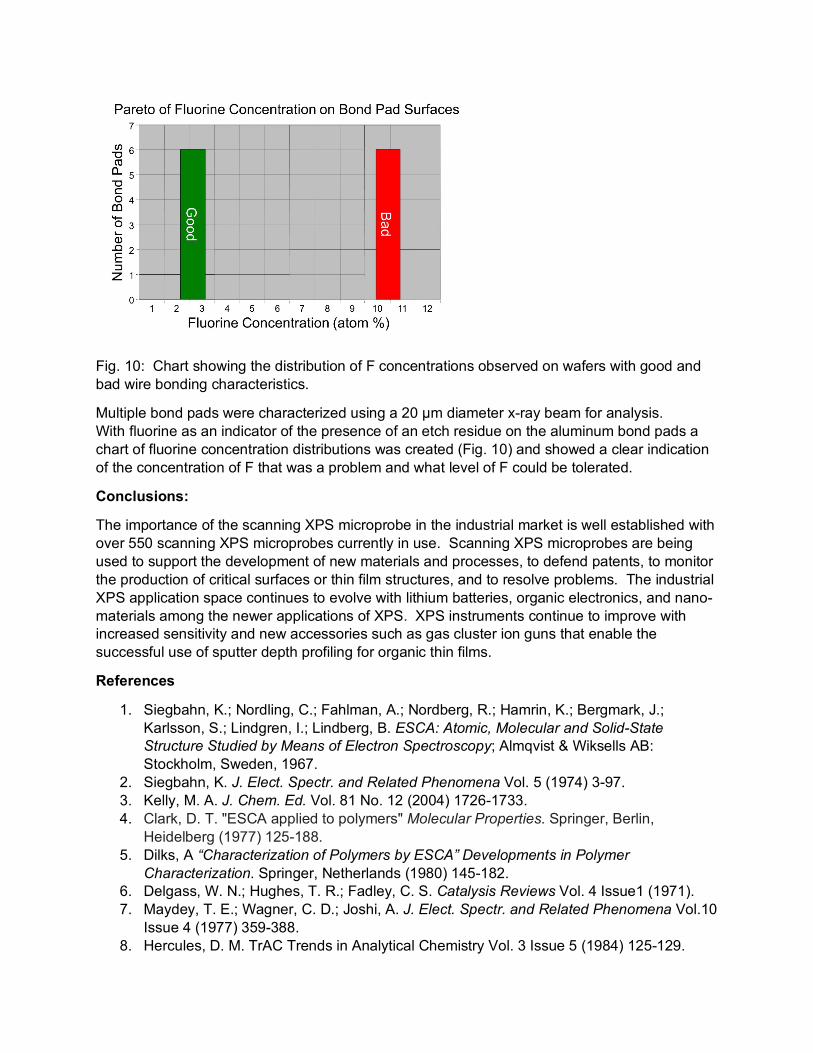
Fig. 10: Chart showing the distribution of F concentrations observed on wafers with good and bad wire bonding characteristics.
Multiple bond pads were characterized using a 20 µm diameter x-ray beam for analysis. With fluorine as an indicator of the presence of an etch residue on the aluminum bond pads a chart of fluorine concentration distributions was created (Fig. 10) and showed a clear indication of the concentration of F that was a problem and what level of F could be tolerated.
Conclusions:
The importance of the scanning XPS microprobe in the industrial market is well established with over 550 scanning XPS microprobes currently in use. Scanning XPS microprobes are being used to support the development of new materials and processes, to defend patents, to monitor the production of critical surfaces or thin film structures, and to resolve problems. The industrial XPS application space continues to evolve with lithium batteries, organic electronics, and nano-materials among the newer applications of XPS. XPS instruments continue to improve with increased sensitivity and new accessories such as gas cluster ion guns that enable the successful use of sputter depth profiling for organic thin films.
References
1. Siegbahn, K.; Nordling, C.; Fahlman, A.; Nordberg, R.; Hamrin, K.; Bergmark, J.; Karlsson, S.; Lindgren, I.; Lindberg, B. ESCA: Atomic, Molecular and Solid-State Structure Studied by Means of Electron Spectroscopy; Almqvist & Wiksells AB: Stockholm, Sweden, 1967.
2. Siegbahn, K. J. Elect. Spectr. and Related Phenomena Vol. 5 (1974) 3-97. 3. Kelly, M. A. J. Chem. Ed. Vol. 81 No. 12 (2004) 1726-1733. 4. Clark, D. T. "ESCA applied to polymers" Molecular Properties. Springer, Berlin,
Heidelberg (1977) 125-188. 5. Dilks, A “Characterization of Polymers by ESCA” Developments in Polymer
Characterization. Springer, Netherlands (1980) 145-182. 6. Delgass, W. N.; Hughes, T. R.; Fadley, C. S. Catalysis Reviews Vol. 4 Issue1 (1971). 7. Maydey, T. E.; Wagner, C. D.; Joshi, A. J. Elect. Spectr. and Related Phenomena Vol.10
Issue 4 (1977) 359-388. 8. Hercules, D. M. TrAC Trends in Analytical Chemistry Vol. 3 Issue 5 (1984) 125-129.

9. Castle, J. E. Surface Science Vol. 68 (1977) 583-602. 10. Linder, R. E.; Mee, P.B. IEEE Trans. on Magnetics Vol. 18 No. 6 (1982) 1073-1076. 11. Adem, E.; Champaneria, R.; Coxon, P. Vacuum Vol. 41 Issues 7-9 (1990) 1695-1699. 12. Larson, P.E.; Palmberg, P.W. Scanning and High Resolution X-ray Photoelectron
Spectroscopy and Imaging, U.S. Patent No. 5315113 (1994). 13. Iwai, H.; Oiwa, R.; Larson, P.E.; Kudo, M. Applied Surf. Sci. Vol. 100-101 (1996) 283-
286. 14. Larson, P. E.; Kelly, M. A. JVST A Vol. 16 Issue 6 (1998) 3483-3489.