industrial usb flash drive module u-400 series symbol test condition min typ max unit supply voltage...
TRANSCRIPT

Product Data Sheet
Industrial USB Flash Drive Module U-400 Series USB2.0 high speed, SLC
Swissbit AG Revision: 1.02 Industriestrasse 4
CH-9552 Bronschhofen www.swissbit.com U-400_data_sheet_Rev102.docx
Switzerland [email protected] Page 2 of 14
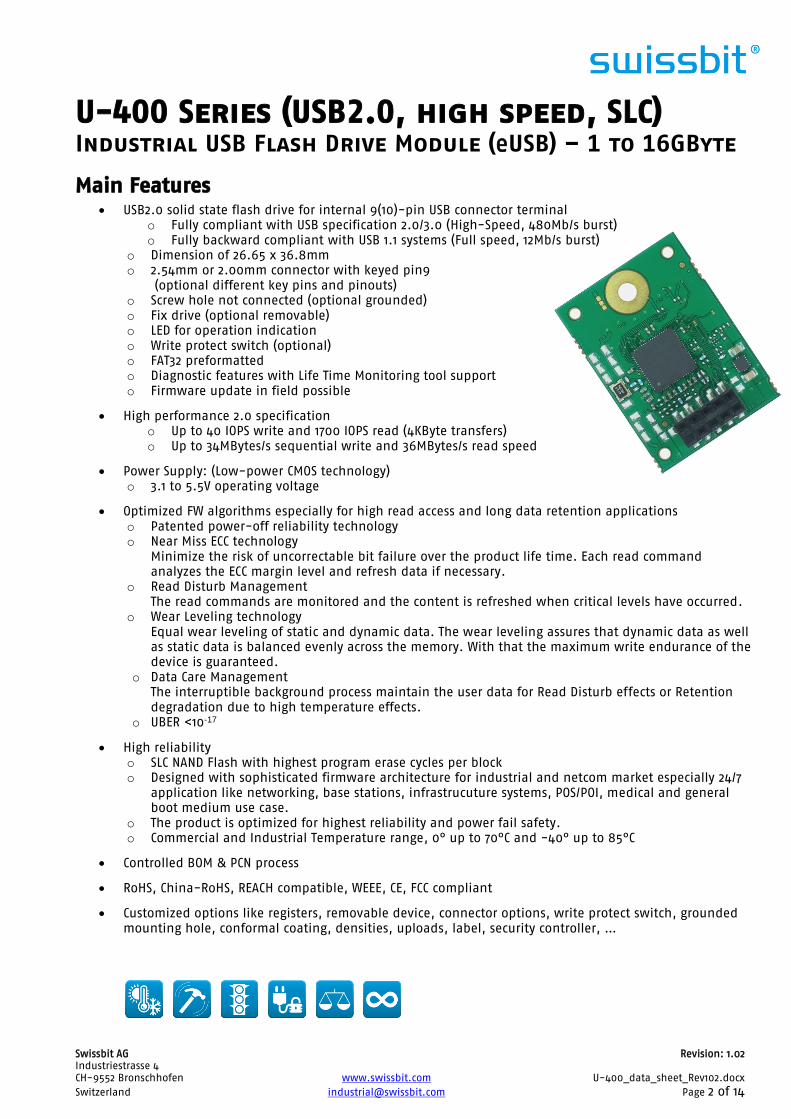
U-400 Series (USB2.0, high speed, SLC)
Industrial USB Flash Drive Module (eUSB) – 1 to 16GByte
Main Features USB2.0 solid state flash drive for internal 9(10)-pin USB connector terminal
o Fully compliant with USB specification 2.0/3.0 (High-Speed, 480Mb/s burst)
o Fully backward compliant with USB 1.1 systems (Full speed, 12Mb/s burst)
o Dimension of 26.65 x 36.8mm
o 2.54mm or 2.00mm connector with keyed pin9
(optional different key pins and pinouts)
o Screw hole not connected (optional grounded)
o Fix drive (optional removable)
o LED for operation indication
o Write protect switch (optional)
o FAT32 preformatted
o Diagnostic features with Life Time Monitoring tool support
o Firmware update in field possible
High performance 2.0 specification
o Up to 40 IOPS write and 1700 IOPS read (4KByte transfers)
o Up to 34MBytes/s sequential write and 36MBytes/s read speed
Power Supply: (Low-power CMOS technology)
o 3.1 to 5.5V operating voltage
Optimized FW algorithms especially for high read access and long data retention applications
o Patented power-off reliability technology
o Near Miss ECC technology
Minimize the risk of uncorrectable bit failure over the product life time. Each read command
analyzes the ECC margin level and refresh data if necessary.
o Read Disturb Management
The read commands are monitored and the content is refreshed when critical levels have occurred.
o Wear Leveling technology
Equal wear leveling of static and dynamic data. The wear leveling assures that dynamic data as well
as static data is balanced evenly across the memory. With that the maximum write endurance of the
device is guaranteed.
o Data Care Management
The interruptible background process maintain the user data for Read Disturb effects or Retention
degradation due to high temperature effects.
o UBER <10-17
High reliability
o SLC NAND Flash with highest program erase cycles per block
o Designed with sophisticated firmware architecture for industrial and netcom market especially 24/7
application like networking, base stations, infrastrucuture systems, POS/POI, medical and general
boot medium use case.
o The product is optimized for highest reliability and power fail safety.
o Commercial and Industrial Temperature range, 0° up to 70°C and -40° up to 85°C
Controlled BOM & PCN process
RoHS, China-RoHS, REACH compatible, WEEE, CE, FCC compliant
Customized options like registers, removable device, connector options, write protect switch, grounded
mounting hole, conformal coating, densities, uploads, label, security controller, …

Swissbit AG Revision: 1.02 Industriestrasse 4
CH-9552 Bronschhofen www.swissbit.com U-400_data_sheet_Rev102.docx
Switzerland [email protected] Page 3 of 14
1 Table of Content MAIN FEATURES ............................................................................................................................................................. 2
1 TABLE OF CONTENT ...................................................................................................................................................... 3
2 ORDER INFORMATION ................................................................................................................................................. 4
2.1 STANDARD PRODUCTS WITH 2.54MM (J) CONNECTOR ..................................................................................................... 4 2.2 LOW PROFILE PRODUCTS WITH 2.00MM (K) CONNECTOR ................................................................................................ 4 2.3 OFFERED OPTIONS FOR CUSTOM PRODUCTS ................................................................................................................... 4
3 NAND FLASH TECHNOLOGIES....................................................................................................................................... 4
4 CAPACITY SPECIFICATION ............................................................................................................................................. 5
5 SYSTEM PERFORMANCE ............................................................................................................................................... 5
6 INTERFACE / PIN OUT .................................................................................................................................................. 5
7 ELECTRICAL SPECIFICATION .......................................................................................................................................... 6
8 ENVIRONMENTAL SPECIFICATION AND RELIABILITY .................................................................................................... 7
8.1 RECOMMENDED OPERATING CONDITIONS ..................................................................................................................... 7 8.2 RELIABILITY .......................................................................................................................................................... 7 8.3 ENVIRONMENTAL - SHOCK, VIBRATION, AND HUMIDITY ................................................................................................ 7
9 COMPATIBILITY & COMPLIANCE .................................................................................................................................. 7
10 APPLICATIONS ............................................................................................................................................................ 8
11 STANDARD FORM FACTORS AND HARDWARE ............................................................................................................. 8
12 BEST PRACTICES ....................................................................................................................................................... 11
12.1 DEVICE REMOVAL & POWER FAILURE ...................................................................................................................... 11 12.2 LIFETIME END HANDLING ...................................................................................................................................... 11
13 PART NUMBER DECODER ......................................................................................................................................... 12
14 LABEL ....................................................................................................................................................................... 13
15 REVISION HISTORY ................................................................................................................................................... 14

Swissbit AG Revision: 1.02 Industriestrasse 4
CH-9552 Bronschhofen www.swissbit.com U-400_data_sheet_Rev102.docx
Switzerland [email protected] Page 4 of 14
2 Order Information Density Part Number Connector Temp. Range Flash Technology
1GB SFUI1024cgAB1TO-t-MS-2xx-STD
c = J 2.54mm pitch
c = K 2.00mm pitch
t = C -0°C to 70°C
t = I -40°C to 85°C SLC NAND Flash
2GB SFUI2048cgAB2TO-t-MS-2xx-STD
4GB SFUI4096cgAB1TO-t-MS-2xx-STD
8GB SFUI8192cgAB2TO-t-MS-2xx-STD
16GB SFUI016GcgAB1TO-t-QT-2xx-STD
g = generation; x = options, firmware and custom configuration
2.1 Standard products with 2.54mm (J) connector
Density Part Number 1GB SFUI1024J1AB1TO-t-MS-211-STD
2GB SFUI2048J1AB2TO-t-MS-211-STD
4GB SFUI4096J1AB1TO-t-MS-211-STD
8GB SFUI8192J1AB2TO-t-MS-211-STD
16GB SFUI016GJ1AB1TO-t-QT-211-STD
2.2 Low profile products with 2.00mm (K) connector
Density Part Number 1GB SFUI1024K1AB1TO-t-MS-211-STD
2GB SFUI2048K1AB2TO-t-MS-211-STD
4GB SFUI4096K1AB1TO-t-MS-211-STD
8GB SFUI8192K1AB2TO-t-MS-211-STD
16GB SFUI016GK1AB1TO-t-QT-211-STD
t = temperature grade (C=0°C to 70°C and I=-40°C to +85°C)
2.3 Offered options for custom products
Removable or fixed drive (standard fix)
Customer specified strings and IDs
FAT16, FAT32 format or customer file system, default FAT32
Preload service
Temperature range
Please ask our sales for more details and additional features.
3 NAND Flash technologies SLC, pSLC and MLC flash
o Single-level-cell (SLC) flash, 1 bit (1 level) is stored in each memory cell
o Pseudo Single-level-cell (pSLC) 1 bit (1 level) is stored in an MLC memory cell by special sequences
o Multi-level-cell (MLC) flash, 2 bit (3 level) are stored in each memory cell
Differences
Series U-400 U-46 U-45
SLC pSLC MLC comment Endurance up to 100,000 up to 20,000 up to 3,000 Physical write/erase cycles
Write Performance Superior Superior High pSLC and SLC have improved write
performance due to single bit write
Read Performance Increased Increased High pSLC and SLC have improved read
performance due to single bit read
Reliability highest high normal Degradation of information has higher
impact with 4 reference levels
Cost high medium low MLC can store twice the bits per square
mm silicon

Swissbit AG Revision: 1.02 Industriestrasse 4
CH-9552 Bronschhofen www.swissbit.com U-400_data_sheet_Rev102.docx
Switzerland [email protected] Page 5 of 14
4 Capacity specification Capacity Sectors Total addressable capacity (Byte)
1GB 1,960,704 1,003,880,448
2GB 3,921,664 2,007,891,968
4GB 7,843,328 4,015,783,936
8GB 15,663,104 8,019,509,248
16GB 31,719,424 16,240,345,088
32GB 62,533,296 32,017,047,552
5 System performance
Speed High Speed mode
(sequential, typ)
Full Speed mode
(sequential, typ)
unit
Burst 480 12 Mbit/s
Read 28 (1) 1.0 MByte/s
Write 19/27 (1) 0.9 1) Effective speed varies with controller, number and type of flash, host, file size, file system and operating system
System Performance High Speed mode typ max Unit
Burst Data transfer Rate (480Mbit/s) 60
MB/s
Sustained Sequential Read
1…2GB 28(1)(2) 34(1)
4GB 28 (1)(2) 36(1)
8…16GB 25(1)(2) 32(1)
Sustained Sequential Write
1…2GB 28(1)(2) 34(1)
4GB 26 (1)(2) 31(1)
8…16GB 23(1)(2) 28(1)
Random Read 4k
1…2GB 1200 (1)(2) 1400(1)
IOPS
4GB 1500 (1)(2) 1700(1)
8…16GB 1500(1)(2) 1700(1)
Random Write 4k
1…2GB 33 (1)(2) 40(1)
4GB 16 (1)(2) 22(1)
8…16GB 18 (1)(2) 25(1) 1) Effective speed varies with controller, number and type of flash, host, file size, file system and operating system
2) performance measured with Crystal Disk Mark performance test
6 Interface / Pin out USB-connector 10pin (2mm or 2.54mm pitch)
USB 2.0 high speed interface, USB1.1 full speed compatible
STD variation
Pin Signal Standard type Optional on request 1 V_Bus Operating voltage
2 NC Not Connected V_Bus
3 D- Data signal pair
4 NC Not Connected
5 D+ Data signal pair
6 NC Not Connected
7 GND Ground
8 NC Not Connected GND
9 NC Keyed at connector not keyed NC or V_Bus
10 Shield Ground (shield) NC, LED out, Reset in
See also chapter (Standard form factors and hardware)
2
4
6
8
10
1
3
5
7

Swissbit AG Revision: 1.02 Industriestrasse 4
CH-9552 Bronschhofen www.swissbit.com U-400_data_sheet_Rev102.docx
Switzerland [email protected] Page 6 of 14
7 Electrical Specification Absolute Maximum Ratings
Parameter Symbol Min Max Unit Power Supply Voltage V_Bus -0.5 6.0
V Voltage on D+ and D- V_Data -0.5 3.6
Commercial Operating Temperature T_A
0 70 °C
Industrial Operating Temperature -40 85
DC characteristics for High-Speed operation (T=25°C, V_Bus=5V or 3.3V)
Parameter Symbol Test condition Min Typ Max Unit Supply Voltage (Standard) V_Bus 3.1(1) 3.3 or
5.00
5.25 V
Write current I_WR
V_Bus=5.0V
100 120
mA Read current I_RD 70 100
Idle current I_IDL 45 60
Suspend current I_CCS 0.8 2.5
High Speed Idle Level V_HSOI V_Bus=5.0V -10 10
mV
High Speed Data Signaling
LOW
V_HSOL V_Bus=5.0V -10 10
High Speed Data Signaling
HIGH
V_HSOH V_Bus=5.0V 360 440
Chirp J Level (differential) V_CHIRPJ V_Bus=5.0V 360 440
Chirp K Level (differential) V_CHIRPK V_Bus=5.0V -440 -360
1) The U-400 devices can be supplied with 5V or with 3.3V.
DC characteristics for Full-Speed operation (T=25°C, V_Bus=5V or 3.3V)
Parameter Symbol Test condition Min Typ Max Unit Supply Voltage (5V Type) V_Bus 3.1(1) 3.3 or
5.00
5.25 V
Write current I_WR
V_Bus=5.0V
80 100
mA Read current I_RD 60 80
Idle current I_IDL 45 60
Suspend current I_CCS 0.8 2.5
Input LOW Voltage V_IL 0.8
V
Input HIGH Voltage V_IH 2
Output LOW Voltage V_OL RL of 1.5kΩ to 3.6V 0.3
Output HIGH Voltage V_OH RL of 15kΩ to GND 2.8 3.6
Output Signal Crossover
Voltage
V_CRS 1.3 2.0
1) The U-400 devices can be supplied with 5V or with 3.3V.

Swissbit AG Revision: 1.02 Industriestrasse 4
CH-9552 Bronschhofen www.swissbit.com U-400_data_sheet_Rev102.docx
Switzerland [email protected] Page 7 of 14
8 Environmental Specification and Reliability
8.1 Recommended operating conditions
Parameter Symbol Min Typ Max Unit Commercial Operating Temperature
T_A 0
25
70
°C Industrial Operating Temperature -40 85
Storage Temperature T_S -40 100(1)
1) Data loss (Retention) is accelerated by high temperature (5 days@100°C is equivalent to 10 years@40°C,
i.e. retention acceleration factor is 700)
8.2 Reliability
Parameter Value Endurance (SLC NAND Flash) Up to 100,000 erases per flash block (JESD 218)
Data reliability (UBER) <10-17 bits read
Error correction code (ECC) correct up to 40-bit errors per 1kB
MTBF / MTTF > 3,000,000 hours
Data retention@40°C (JESD 218) 10 years @ 10% life time / 1 years @ life end
Durability > 1,500 insertions / removals
8.3 Environmental - Shock, Vibration, and Humidity
Parameter Value
Shock 1,500G Peak, 0.5m pulse duration, 6 axes
(JESD22-B110 / B104)
Vibration 50G Peak, 20-2,000Hz, 0.75mm, 4 cycles per direction (X, Y and Z)
(MIL-STD-883H M2007.3)
Humidity 85°C, 85% RH, Vmax
(JESD22-A101)
Free fall / Drop test 1.5m
(IEC 60068-2-32)
Temperature Cycles -40°C/+125°C 1000 cycles
(JESD22-A104)
Hazardous gases SO2/H2S 10 days
(IEC 60068-42/43)
9 Compatibility & Compliance Configurable as boot-drive
Standard fix Configuration (mounted as local drive, not as removable drive)
Operating Systems:
o Windows CE
o Windows Server 2003 and 2008
o Windows 10, 8, 7, Vista, XP, 2000, ME
o Mac 9.0 and newer
o Mac 8.6 (with driver) and newer
o Linux 2.4 and newer
o All USB mass-storage host systems (guarantee on all USB-IF certified systems)
CE – EN 55022/55024
FCC class B for information technology
USB-IF high speed certified
RoHS
UL60950 compliant PCB
WEEE

Swissbit AG Revision: 1.02 Industriestrasse 4
CH-9552 Bronschhofen www.swissbit.com U-400_data_sheet_Rev102.docx
Switzerland [email protected] Page 8 of 14
10 Applications Gaming
Industrial PCs
Point-Of-Sale (POS)
Industrial Automation
Networking Equipment
Medical Equipment
Data Recorders
11 Standard form factors and hardware Standard form factor of PCBs 36.8mm x 26.65mm
Hole for mechanical fixture (optional grounded)
Shield (connector Pin 10) grounded (optional NC)
2 additional holes
LED for operation indication (optional no LED)
2 connector types
o 2.54mm pitch, 7.5mm long standard
o 2.00mm pitch, 3.6mm long low profile
Component heights max. 1.6mm on connector side
max. 1.2mm on flash side
Figure 1: Mechanical Dimensions for 2.54mm connector (standard)
Swissbit AG Revision: 1.02 Industriestrasse 4
CH-9552 Bronschhofen www.swissbit.com U-400_data_sheet_Rev102.docx
Switzerland [email protected] Page 9 of 14
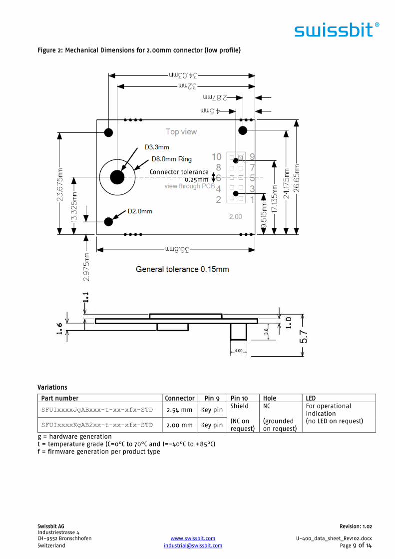
Figure 2: Mechanical Dimensions for 2.00mm connector (low profile)
Variations
Part number Connector Pin 9 Pin 10 Hole LED
SFUIxxxxJgABxxx-t-xx-xfx-STD 2.54 mm Key pin Shield
(NC on
request)
NC
(grounded
on request)
For operational
indication
(no LED on request) SFUIxxxxKgAB2xx-t-xx-xfx-STD 2.00 mm Key pin
g = hardware generation
t = temperature grade (C=0°C to 70°C and I=-40°C to +85°C)
f = firmware generation per product type
Connector tolerance
0.25mm

Swissbit AG Revision: 1.02 Industriestrasse 4
CH-9552 Bronschhofen www.swissbit.com U-400_data_sheet_Rev102.docx
Switzerland [email protected] Page 10 of 14
Figure 3: Component region on connector side (general tolerance ±0.5mm)
Figure 4: Component region on flash side (symmetric to center line, general tolerance ±0.5mm)

Swissbit AG Revision: 1.02 Industriestrasse 4
CH-9552 Bronschhofen www.swissbit.com U-400_data_sheet_Rev102.docx
Switzerland [email protected] Page 11 of 14
12 Best Practices There are a number of best practices to reach the maximum life time.
12.1 Device Removal & Power Failure User data can be lost or corrupted if power is interrupted while the UFD is writing data. To avoid data loss, it is
necessary to avoid power interruption while the device is busy. This can be made sure by always using the host
(e.g. Windows) shutdown mechanisms or by detaching the device in the operating system before unplugging it.
Swissbit also offers an Application Note “Design-In Guide” that describes techniques to reduce data loss on
power failure, if power failure absolutely can’t be avoided.
12.2 Lifetime end handling If the flash reaches its end of life, the number of bad blocks will increase (bad flash blocks will be replaced with
spare blocks). There exist different side effects with negative data influence by degraded flash cells. Sometimes
bit errors can occur because of effects that are not immediately detected by the flash, e.g. effects like program
disturb or read disturb, which means that the bad block recognition does not always prevent data loss.
When the number of bit errors in a sector exceeds the ECC correcting capabilities, invalid (uncorrected) data
cannot be read from the host. Because of these effects it is strongly recommended to replace devices that are
nearing their end of life. One good indicator would be the current spare blocks should not be reducing below 5.
It is in the responsibility of the system integrator to account for the flash usage. Swissbit offers support for
calculating expected life time if the exact use case is provided (e.g. by providing low level [USB interface] write
statistics).
For notes on reducing flash stress, Swissbit offers an Application Note called “Design-In Guide”.
Please contact your sales channel for more information or send a mail to [email protected].

Swissbit AG Revision: 1.02 Industriestrasse 4
CH-9552 Bronschhofen www.swissbit.com U-400_data_sheet_Rev102.docx
Switzerland [email protected] Page 12 of 14
13 Part Number Decoder
S F UI 016G J 1 A B 1 TO - I - Q T - 211 - STD
1 2 3 4 5 6 7 8 9 10 11 12 13 14 15
Manuf. Option
Memory Type. Configuration
Product Type Manuf. Code: Flash Mode
Density Manuf. Code: Flash Package
Platform Temp. Option
Product Generation Flash vendor Code
Memory Organization Number of flash chips/channels
Technology
1. Manufacturer
Swissbit S
2. Memory Type
Flash F
3. Product Type
U-xxx USB Flash Drive Module (Internal) UI
4. Density
1 GB 1024
2 GB 2048
4 GB 4096
8 GB 8192
16 GB 016G
5. Platform
U-xxx – 2.54mm plug J
U-xxx – 2.00mm plug K
6. Product Generation
7. Memory Organization
x8 A
8. Technology
U-4xx technology B
9. Number of Flash chips
1 Flash 1
2 Flash 2
10. Flash Code
Toshiba TO
11. Temp. Option
Industrial Temp. Range -40°C to 85°C I
Standard Temp. Range 0°C to 70°C C
12. DIE Classification
SLC MONO (single die package) M
SLC DDP (dual die package) D
SLC QDP (quad die package) Q
13. PIN Mode
Normal nCE & R/nB S
Dual nCE & Dual R/nB T

Swissbit AG Revision: 1.02 Industriestrasse 4
CH-9552 Bronschhofen www.swissbit.com U-400_data_sheet_Rev102.docx
Switzerland [email protected] Page 13 of 14
14. UFD XYZ
X Setting
Removable Drive 1
Fix Drive 2
Y Firmware revision per product generation
Block Based Revision 1, 2, 3, … 1,2,3…
durabit Revision 1, 2, 3, … A,B,C…
Z Optional setting
default 1
pSLC (pseudoSLC) P
15. Option
Swissbit / Standard 5V supply STD
Customized version XXX
14 Label
SFUIxxxxxxABxxx Part Number
-x-xx-xxx-xxx
60xxxxxx Lot Code
6xxxxx Type No.
SFUIxxxxxxABxTO -x-xx-xxx-xxx 60xxxxxx 6xxxxx

Swissbit AG Revision: 1.02 Industriestrasse 4
CH-9552 Bronschhofen www.swissbit.com U-400_data_sheet_Rev102.docx
Switzerland [email protected] Page 14 of 14
15 Revision History
Document Revision History Date Revision Description Revision Detail
05-October-2015 1.00 Initial release Doc. req. no. 0792
15-February-2016 1.01 2.00mm connector position tolerance added Doc. req. no. 0963
27-February-2017 1.02 Added capacity specification and NAND flash technologies
Update performance values, interface illustration, wording
adjustment and removed RoHS, ACPEIP and WEEE decl.
Doc. req. no. 1568
Disclaimer:
No part of this document may be copied or reproduced in any form or by any means, or transferred to any third
party, without the prior written consent of an authorized representative of Swissbit AG (“SWISSBIT”). The
information in this document is subject to change without notice. SWISSBIT assumes no responsibility for any
errors or omissions that may appear in this document, and disclaims responsibility for any consequences
resulting from the use of the information set forth herein. SWISSBIT makes no commitments to update or to keep
current information contained in this document. The products listed in this document are not suitable for use in
applications such as, but not limited to, aircraft control systems, aerospace equipment, submarine cables,
nuclear reactor control systems and life support systems. Moreover, SWISSBIT does not recommend or approve the
use of any of its products in life support devices or systems or in any application where failure could result in
injury or death. If a customer wishes to use SWISSBIT products in applications not intended by SWISSBIT, said
customer must contact an authorized SWISSBIT representative to determine SWISSBIT willingness to support a
given application. The information set forth in this document does not convey any license under the copyrights,
patent rights, trademarks or other intellectual property rights claimed and owned by SWISSBIT. The information
set forth in this document is considered to be “Proprietary” and “Confidential” property owned by SWISSBIT.
ALL PRODUCTS SOLD BY SWISSBIT ARE COVERED BY THE PROVISIONS APPEARING IN SWISSBIT,S TERMS AND CONDITIONS OF
SALE ONLY, INCLUDING THE LIMITATIONS OF LIABILITY, WARRANTY AND INFRINGEMENT PROVISIONS. SWISSBIT MAKES NO
WARRANTIES OF ANY KIND, EXPRESS, STATUTORY, IMPLIED OR OTHERWISE, REGARDING INFORMATION SET FORTH HEREIN OR
REGARDING THE FREEDOM OF THE DESCRIBED PRODUCTS FROM INTELLECTUAL PROPERTY INFRINGEMENT, AND EXPRESSLY
DISCLAIMS ANY SUCH WARRANTIES INCLUDING WITHOUT LIMITATION ANY EXPRESS, STATUTORY OR IMPLIED WARRANTIES OF
MERCHANTABILITY OR FITNESS FOR A PARTICULAR PURPOSE.
©2017 SWISSBIT AG All rights reserved.