inelastic transport in carbon nanotube electronic a nd
TRANSCRIPT

INELASTIC TRANSPORT IN CARBON NANOTUBE ELECTRONIC AND
OPTOELECTRONIC DEVICES
A Dissertation
Submitted to the Faculty
of
Purdue University
by
Siyuranga O. Koswatta
In Partial Fulfillment of the
Requirements for the Degree
of
Doctor of Philosophy
May 2008
Purdue University
West Lafayette, Indiana

ii
To my ever loving parents…

iii
ACKNOWLEGEMENTS
The work presented in this thesis is a product of many fruitful collaborations that I
was fortunate to have during my PhD career. First of all, I thank Professor Mark
Lundstrom for his guidance and mentorship during all this time. His work ethic and the
professional conduct are truly admirable. His preference to allow the students to be the
“decision makers” with respect to their own research, and advising (sometimes insisting)
on recognizing the “bigger picture” issues led to my own professional development. It
was a privilege for me to do my PhD thesis under his guidance.
I am indebted to Dr. Dmitri Nikonov for a very productive and synergistic
collaboration over the years that led to many publications. His involvement in the code
development, especially in introducing phonon scattering in the NEGF simulator, was
instrumental for the rapid progress of this work. I thank him for serving in my PhD
committee, and being the mentor for the graduate fellowship award by the Intel
Foundation. I also thank Dr. Phaedon Avouris of IBM T. J. Watson Research Center for a
fruitful collaboration and summer internship opportunities. I am very grateful to Professor
Ashraf Alam and Professor Supriyo Datta for their advice and serving in my PhD
committee. I have learnt a lot from Professor Datta, taking his quantum transport class
twice, first to learn, and then to understand, and from many of his lectures. More
importantly, his teaching allowed me to develop the intuitive thinking process essential
for a bottom-up future.
I also thank my group members, both past and present, for their insights on many
research topics, and more importantly, for their friendship over the years. I am grateful to

iv
Prof. Jing Guo (now at University of Florida) for the initial matlab simulator that treated
ballistic transport in CNTFETs. It allowed me to get involved in research from the very
beginning. I was also very fortunate for the collaboration with Dr. Sayed Hasan (now at
Intel Corp.). His detailed calculations of phonon modes and electron-phonon coupling
parameters in CNTs made this thesis work that much rigorous. I also benefitted from his
initial work on the numerical solution of the Boltzmann transport equation that I was later
able to extend to modeling CNT based optoelectronic devices. I also thank Dr. Jing Wang
(now at IBM Corp.), and EE350 colleagues Neophytos Neophytou, Yang Liu, Himadri
Pal, Raseong Kim, Yunfei Gao, Changwook Jeong, Tony Low, Lutfe Siddiqui, Sayeef
Salahuddin, Ninad Pimparkar, Bhaskaran Muralidharan, Kirk Bevan, and Ehtesham Islam
for many fruitful discussions at many occasions.
Finally, many thanks to the NSF funded Network for Computational
Nanotechnology (NCN) center for almost infinite computer resources.

v
TABLE OF CONTENTS Page LIST OF TABELS .....................................................................................................vi LIST OF FIGURES....................................................................................................vii ABSTRACT ............................................................................................................xv 1. INTRODUCTION.................................................................................................1 2. NEGF TREATMENT OF BALLISTIC TRANSPORT IN CNT TRANSISTORS....................................................................................................10 2.1. NEGF Treatment of Transport ...............................................................10 2.2. Poisson’s Equation.................................................................................18 3. NEGF TREATMENT OF DISSIPATIVE TRANSPORT IN CNT TRANSISTORS....................................................................................................21 3.1. Phonon Modes in a CNT........................................................................22 3.2. Electron-Phonon Scattering ...................................................................26 3.3. Numerical Treatment of Dissipative Transport .....................................28 3.3.1. Treatment of optical phonon scattering ..................................28 3.3.2. Treatment of acoustic phonon scattering ................................29 4. EFFECT OF PHONON SCATTERING IN CNT-MOSFETS .............................31 4.1. Effect of Phonon Scattering on Conventional Operation of CNT-MOSFETs.....................................................................................31 4.2. Phonon-Assisted Inelastic Tunneling in CNT-MOSFETs.....................39 5. INFLUENCE OF PHONON SCATTERING IN CNT P-I-N TUNNEL TRANSISTORS...................................................................................50 5.1. Background on p-i-n Tunnel Transistors ...............................................50 5.2. Ballistic Operation of p-i-n TFETs ........................................................52 5.3. Influence of Phonon Scattering on Above-Threshold Operation...........55

vi
Page 5.4. Influence of Phonon Scattering on Subthreshold Operation..................58 6. PERFORMANCE COMPARISON BETWEEN CNT BASED P-I-N TUNNEL FET AND CONVENTIONAL MOSFET GEOMETRIES..................61 6.1. Comparison of the Off-State Operation .................................................62 6.1.1. Subthreshold slope, off-current (IOFF), and standby power dissipation (Pstandby) ........................................63 6.1.2. Comparative influence of phonon scattering ..........................66 6.1.3. Drain induced off-state degradation........................................67 6.2. Comparison of the On-State Performance .............................................69 6.2.1. On-current (ION) ......................................................................70 6.2.2. Intrinsic device delay metric () ..............................................71 6.2.3. Power-delay product (PDP) and Dynamic power dissipation (Pdynamic) .....................................................73 6.3. Device Operation at the Quantum Capacitance Limit ...........................75 7. TREATMENT OF INELASTIC TRANSPORT IN CNT OPTOELECTRONIC DEVICES..........................................................................79 7.1. Background on Excitonic Emission in CNTs ........................................79 7.2. Simulation Method ................................................................................83 7.2.1. Numerical solution of the Botzmann transport equation (BTE)........................................................................83 7.2.2. Finite difference solution of the Poisson’s equation...............89 8. EXCITON GENERATION IN CNTS FOR OPTOELECTRONIC APPLICATIONS ..................................................................................................94 9. CONCLUSION AND FUTURE WORK..............................................................105 9.1 CNT Electronics and Band-to-Band Tunneling Devices ...................105 9.2 CNT Optoelectronic Devices .............................................................107 9.3 Future Outlook ...................................................................................108 LIST OF REFERENCES ...........................................................................................110

vii
LIST OF TABLES
Table Page 4.1 Phonon energy and e-ph coupling parameters for the CNTs used in this study ........................................................................................................32 7.1 Comparison of excitonic properties for conventional semiconductors vs. CNTs ..............................................................................82
viii
LIST OF FIGURES Figure Page 1.1 Scaling of the physical dimensions of CMOS transistors [1] ........................1 1.2 (a) Power dissipation in Intel microprocessors (www.intel.com), (b) Power dissipation and technological evolution. Adapted from an article by T. C. Chen (IBM); available at www.ieee.org ...............................2 2.1 (a) Device structure with wrap-around gate, (b) NEGF model with coupling to the phonon bath, and (c) mode-space Hamiltonian. ..................11 2.2 Self-consistency requirement between NEGF and Poisson solutions............18 3.1 Lowest energy degenerate subbands in a CNT corresponding to K and K/ valleys of 2D graphene Brillouin zone. (a) and (b) show intra-valley and inter-valley scattering processes, respectively .....................22 3.2 Energy dispersion for phonon modes in a (16,0) CNT: (a) zone-center phonons that allow intra-valley scattering and, (b) zone-boundary phonons that allow inter-valley scattering. Modes that effectively couple to the electrons are indicated by dashed circles. Zone-boundary phonons are composed of a mixture of fundamental polarizations ...............24 4.1 IDS-VDS for the (16,0) CNTFET under ballistic transport, OP scattering (all modes together), and AP scattering. High-energy OP scattering becomes important at sufficiently large gate biases. Until then AP and RBM scattering are dominant. ................................................................33 4.2 IDS-VGS for the (16,0) CNTFET at VDS = 0.3V under ballistic transport, OP scattering (all modes together), and AP scattering. The inset shows that acoustic phonons are more detrimental up to moderate gate biases ......................................................................................................34

ix
Figure Page 4.3 Energy-position resolved current spectrum for (16,0) CNTFET at VGS = 0.5V, VDS = 0.5V (logarithmic scale). (a) ballistic, (b) dissipative transport (all OP modes together). Thermalization near the drain end by emitting high-energy OPs leaves the electrons without enough energy to overcome the channel barrier .........................................................................35 4.4 Energy-position resolved electron density spectrum for (16,0) CNTFET at VGS = 0.5V, VDS = 0.5V. (a) ballistic, (b) dissipative transport (all OP modes together). Quantized states in the valence band are broadened, and give rise to many phonon induced side-bands. The interference pattern for conduction band states are also broadened compared to the ballistic case .............................................................................................37 4.5 Ballisticity (Iscat/Iballist) vs. FSη for (16,0), (19,0) and (22,0) CNTFETs, (a) with all OP modes together, (b) with AP scattering. FSη is defined as the energy difference between the source Fermi level and the channel barrier (see Figure 4.3(b)).................................................................38 4.6 Experimental IDS-VGS data at different VDS biases for the p-type CNT-MOSFET; reproduced from Ref. [42] ..................................................42 4.7 BTBT operation in a p-type CNT-MOSFET: (a) For large positive VGS, direct tunneling of electrons from drain to source through the quantized conduction band states in the channel region, (b) For moderately positive VGS direct tunneling is prohibited, but inelastic tunneling is possible in the presence of optical phonons (dashed arrows), (c) NEGF simulation results for energy-position resolved current density spectrum (logarithmic scale) under 195meV LO phonon scattering at VGS = 0.4V, VDS = -0.3V.................................................................................43 4.8 Simulated IDS-VGS characteristics for the p-type CNT-MOSFET (black solid line - 60mV/dec swing): (a) ballistic, (b) one-phonon scattering with 195meV LO mode..................................................................................45 4.9 Simulated IDS-VGS with only one-phonon scattering due to 195meV zone center LO mode (solid lines) and, also including two-phonon scattering due to 2 x 180meV zone-boundary mode (dashed lines). Red-star, blue-circle, and green-square curves are at the same voltages as in Figure 4.8(b), magenta-triangle curves are at VDS = -0.6V. ..................................................47

x
Figure Page 5.1 (a) Gated CNT p-i-n Tunnel FET with wrapped around high-k cylindrical gate geometry, (b) Equilibrium band diagram for the p-i-n Tunnel FET. A (13,0) zigzag CNT with EG 0.8eV is being used. ...................................52 5.2 (a) Energy-position resolved electron density distribution, (b) Energy-position resolved current density distribution (log scale). ...........53 5.3 IDS-VDS results for CNT p-i-n Tunnel FET shown in Figure 5.1. VGS is varied from 0 to 0.6V in steps of 0.1V. A (13,0) zigzag CNT is used...........55 5.4 (a) Above-threshold IDS-VDS characteristics for the CNT p-i-n TFET. All the optical phonon modes (LO, ZBO, and RBM) are considered simultaneously for OP scattering. LA mode is considered for AP scattering. (b) Energy-position resolved current density spectrum (i.e., integrand of Eq. (2.18)) at VDS = VGS = 0.5V confirms the reduced influence of high-energy OP scattering on DC current transport up to moderate gate biases. .............................................................57 5.5 (a) IDS-VGS characteristics for the CNT p-i-n TFET at VDS = 0.1V and 0.4V with and without phonon scattering. Simulated device temperatures are as shown in the legend. (b) Energy-position resolved current density spectrum at a device temperature of 400K (VGS = 0.125V, VDS = 0.1V). Phonon absorption assisted transport is clearly observed at the source- channel junction. Carriers thermalize after reaching the drain. .....................59 6.1 The modeled device geometry used in this study with cylindrically symmetric wrap-around gate electrode (see text for device parameters). The high-k oxide is removed from source/drain regions in order to reduce the fringing fields that adversely affect the drive current for the p-i-n TFET..........................................................................................62 6.2 IDS-VGS dependence on temperature for, (a) n-i-n MOSFET and, (b) p-i-n TFET under ballistic and dissipative transport. The latter has reduced temperature dependence under ballistic conditions. Phonon assisted tunneling can, however, degrade the subthreshold characteristics.................................................................................................63 6.3 Band diagram and the source Fermi distribution for, (a) n-i-n MOSFET and, (b) p-i-n TFET. In the latter, high-energy part of the source distribution is cutoff by the bandgap region leading to < 60mV/decade subthreshold swing. Phonon assisted tunneling becomes important under these conditions. ...................................................64

xi
Figure Page 6.4 IOFF vs. ION dependence on temperature at VDD = 0.3V under, (a) ballistic and, (b) dissipative transport. Shaded region is where the p-i-n TFET has an advantage over the n-i-n MOSFET due to larger ION with a smaller IOFF. Temperature dependence of IOFF for the p-i-n TFET is also smaller than that for the latter.................................................................65 6.5 Dependence of subthreshold properties on the drain bias for, (a) n-i-n MOSFET and, (b) p-i-n TFET under ballistic transport (the device geometry is slightly modified from that for the rest of the paper. See text for details). The n-i-n MOSFET shows small DIBL compared to the p-i-n TFET. For the latter the off-current is increased at high VDS due to drain induced barrier shortening (DIBS) (see Figure 6.6). ........................68 6.6 Band diagram in the off-state for, (a) n-i-n MOSFET and, (b) p-i-n TFET at different drain biases. For the latter, drain induced barrier shortening (DIBS) is observed which increases the tunneling current through the channel barrier exponentially......................................................69 6.7 Linear IDS-VGS comparison for the n-i-n MOSFET and p-i-n TFET under ballistic and dissipative transport. The on-current for the latter is reduced due to the presence of the tunneling barrier..................................70 6.8 Intrinsic device delay metric () vs. ION/IOFF comparison. Surprisingly, p-i-n TFET shows similar delay compared to the n-i-n MOSFET even though the former has a smaller drive current (Figure 6.7). Also, p-i-n TFET even becomes faster at larger ION/IOFF operating regime. In the presence of a load capacitance, however, the actual drive current will become important and the p-i-n TFET could be relatively slower. ........71 6.9 Comparison of the power-delay product (PDP = switching energy). p-i-n TFET has a significant benefit here, and shows a fundamentally different behavior compared to the n-i-n MOSFET.......................................73 6.10 Total device capacitance ( gC ) vs. VGS calculated from tot GSdQ V for, (a) n-i-n MOSFET and, (b) p-i-n TFET under dissipative transport. At small VDS both devices show similar characteristics. However, at larger VDS a fundamentally different behavior is observed; for the p-i-n TFET device capacitance remains small until larger gate biases are applied. .....................................................................................................74

xii
Figure Page 6.11 Energy-position resolved electron distribution for, (a) n-i-n MOSFET and, (b) p-i-n TFET under ballistic transport at VGS = 0.5V, VDS = 0.3V. A significantly higher occupation of channel states is observed for the former..................................................................................75 6.12 Reservoir resolved LDOS for the n-i-n MOSFET at VGS = 0.5V, VDS = 0.3V: (a) source-evolving states (LODSS), (b) drain-evolving states (LDOSD). There is a significant amount of source-evolving states inside the channel that are filled by the source Fermi distribution. Drain-evolving states in the channel are not filled at larger VDS....................76 6.13 Reservoir resolved LDOS for the p-i-n MOSFET at VGS = 0.5V, VDS = 0.3V: (a) source-evolving states (LODSS), (b) drain-evolving states (LDOSD). There is a small amount of source-evolving states inside the channel due to the presence of the tunneling barrier. These are the states filled by the source Fermi distribution. Interestingly, there is a significant amount of drain-evolving states inside the channel but they are not filled at large VDS..................................................................77 7.1 (a) A schematic of the CNTFET suspended over a trench with the back-gated geometry, (b) Experimental observation of optical emission localized at the trench-drain junction (from [10]). (c) Band diagram near the trench-substrate junction at the drain end (shown for VGS > 0). Electrons that are injected from the source can gain enough kinetic energy at this junction for the impact excitation of excitons. ........................81 7.2 Self-consistent BTE-Poisson iteration scheme used in this study .................84 7.3 Treatment of SB-tunneling near the source end. Phase-space distribution function, f(z,k), at the position zi is considered...........................86 7.4 (a) 2D finite difference mesh for solving Poisson’s equation in a cylindrically symmetric geometry. (b) Grid points around element (m,n) .....89 7.5 Discretization scheme at the boundary between two dielectric regions in and out. In this case mesh elements are created such that the boundary completely lies within them .....................................................90 8.1 Model device structures used in this study; (a) partially suspended CNT-MOSFET with doped source/drain contacts, (b) partially suspended SB-CNTFET with metal Schottky contacts. ................................94

xiii
Figure Page 8.2 (a) Band diagram for the (25,0) zigzag CNT-MOSFET at VGS = 0.7V and VDS = 0.8V calculated from self-consistent simulation. (b) Energy-position resolved electron distribution function. Note that positive (negative) energy represents positive (negative) going carries with +k (–k) momentum. Degenerately doped source/drain regions are clearly visible at the ends. ...........................................................95 8.3 (a) Band diagram for the (25,0) SB-CNTFET at VGS = 0.8V and VDS = 0.7V calculated from self-consistent simulation. (b) Energy-position resolved electron distribution function for the above device. Note that positive (negative) energy represents positive (negative) going carries with +k (–k) momentum. A significant hot-electron population is seen at the trench-substrate junction near the drain-end (Line-(B)). ........................................................................97 8.4 The distribution function at Line-(B) of Figure 8.3 (b) (z = 10nm). As earlier, positive (negative) energy represents positive (negative) going carries with +k (–k) momentum. The significant population of hot-electrons in this region can scatter to empty low-energy states by the following processes: (a) OP forward emission into the +kfinal state, (b) OP backward emission into the –kfinal state, or, (c) high-energy exciton emission that scatters electrons down to the states near the bottom of the band (E 0). ............................................................................98 8.5 (a) Steady-state exciton generation profile along the CNT for the device shown in Figure 8.3. Localized exciton generation near the trench-substrate junction is clearly observed (dashed circle). The radiative recombination of these excitons leads to localized optical emission seen in the experiment. Additional exciton generation near the drain contact is also observed. (b) The generation profile (solid) along with the electric field (dashed) near the trench-substrate junction. The highest generation region is located to the right of the high-field region. .................................................................................100

xiv
Figure Page 8.6 (a) IDS-VGS comparison at VDS = 0.7V for a (25,0) SB-CNTFET. Device parameters used here are similar to that in Figure 8.3 (a) except for Ttrench and the substrate oxide. TOX = 10nm, OX = 3.9 (SiO2) and OX = 16 (HfO2) have been used. A linear increase in IDS is observed above the threshold voltage. On-current is reduced for the deeper trench due to reduced gate coupling in that region. (b) Exciton generation efficiency at the trench-substrate junction vs. VGS shows an exponential increase. Exciton generation for a (19,0) CNT device with SiO2 substrate oxide and Ttrench = 10nm (dash-dot curve) is compared to that of the (25,0) CNT devices (see legend of (a))....................102

xv
ABSTRACT Koswatta, Siyuranga O. Ph.D., Purdue University, May 2008. Inelastic Transport in Carbon Nanotube Electronic and Optoelectronic Devices. Major Professor: Mark S. Lundstrom.
Discovered in the early 1990’s, carbon nanotubes (CNTs) are found to have
exceptional physical characteristics compared to conventional semiconductor materials,
with much potential for devices surpassing the performance of present-day electronics.
Semiconducting CNTs have large carrier mobilities and a direct electronic bandgap,
resulting in enhanced band-to-band tunneling (BTBT) as well as optical properties that
could lead to novel electronic and optoelectronic applications. Therefore, detailed
modeling and simulation of electronic transport in CNTs is required for a comprehensive
understanding of the operation of CNT based devices. We have used the nonequilibrium
Green’s function (NEGF) formalism for dissipative quantum transport simulation of CNT
field-effect transistors. Previous experiments have shown that BTBT in CNT-MOSFETs
can lead to subthreshold swings below the 60mV/decade conventional limit, which makes
these devices promising candidates for low-power applications. Our simulations indeed
confirm this observation, and further show that this regime of operation is dominated by
phonon-assisted tunneling which degrades desirable device behavior. A detailed
investigation of a CNT based p-i-n tunneling transistor (TFET) geometry that has much
favorable device characteristics is also presented. We observe less than 60mV/decade
subthreshold swing for this geometry that leads to smaller off-state leakage and standby
power dissipation compared to the conventional MOSFET operation. Under on-state
performance, the drive current and the switching speed of p-i-n TFETs are dominated by
the tunneling barrier properties. Interestingly, the switching energy of the p-i-n TFET is
observed to be fundamentally smaller than that for the MOSFET at the quantum

xvi
capacitance limit of operation. Finally, a study on the modeling and simulation of
inelastic transport in a CNT based optoelectronic device using the semiclassical
Boltzmann transport equation is presented. The optical emission in these devices is
attributed to an excitonic process. Localized exciton generation under high-field
conditions is explored, and detailed device optimization schemes are discussed. These
devices have the potential for ultra-bright light emission, among many other
optoelectronic applications.

1
1. INTODUCTION
With continual scaling of the CMOS transistor, first demonstrated in the early
1960’s, the semiconductor electronics industry is reaching a crossroads. The scaling has
allowed exponential improvements in circuit performance over the decades and the
device dimensions are soon reaching the atomic scales (Figure 1.1) [1]. The exponential
enhancements, however, have come with a concomitant increase in circuit power
dissipation. The present day microchips dissipate about 100W of power which is at the
limit of economically feasible heat sinking technologies (Figure 1.2 (a)). Therefore, the
continued scaling and the increase in transistor densities have led to power-performance
tradeoffs, resulting in modern architectural solutions as multicore processors. Recent
introduction of high-k oxides into semiconductor technology has alleviated the problem
of gate leakage and allowed further scaling of device dimensions [2]. The basic
Figure 1.1. Scaling of the physical dimensions of CMOS transistors [1].

2
operational principles of thermal MOSFETs, however, have imposed fundamental limits
on power dissipation in conventional CMOS technology that would be aggravated with
continual increase in device densities. From a historical point of view, it is interesting to
note that the semiconductor industry has indeed gone through technological “revolutions”
due to power dissipation constraints, such as the move from bipolar devices to CMOS
itself (Figure 1.2 (b)). Therefore, it is quite likely that the performance evolutions of the
CMOS transistor might be coming to a roadblock, and a new technological “revolution”
is called for.
Carbon nanotubes (CNTs), first discovered in the early 1990’s [3, 4], have proved
to possess exceptional physical properties compared to all conventional semiconducting
materials [5]. They have carrier mobilities of 104~105 cm2/Vs [6, 7] so high-performance
electronic devices are possible. The conduction and the valence band effective masses in
CNTs are small and they are the same; their band dispersions are approximately
symmetric (they are exactly symmetric according to nearest-neighbor tight-binding
calculations) [8]. This symmetry leads to equal performance for n-type and p-type
transistors, which is a technologically desirable property. Semiconducting CNTs also
Figure 1.2. (a) Power dissipation in Intel microprocessors (www.intel.com), (b) Power dissipation and technological evolution. Adapted from an article by T. C.
Chen (IBM); available at www.ieee.org.
3
possess a direct electronic bandgap so they have increased band-to-band tunneling
(BTBT) properties, as well as enhanced optical activity [9-12], that could lead to novel
electronic and optoelectronic applications [5]. High-performance CNT transistors
operating close to the ballistic limit have already been experimentally demonstrated [13-
16]. Therefore, CNTs have been extensively investigated due to their aforementioned
attractive properties that might be employed in solving some of the pressing challenges of
the 21st century.
Nevertheless, phonon scattering in CNTs can influence their ballistic
performance, and can be important for devices with channel lengths of a few 10’s of
nanometers or more [17-19]. Therefore, computational simulations rigorously treating
both quantum and incoherent effects are imperative for a comprehensive understanding of
the operation, and the deterministic modeling, of these devices. The nonequilibrium
Green’s function (NEGF) formalism has provided a universal framework in treating
dissipative quantum transport in nanoscale devices [20-23]. In NEGF formalism the
electronic structure of the device can be described by simpler models such as the
effective-mass Hamiltonian, or, more accurate models such as atomistic tight-binding or
ab initio descriptions. Important quantum mechanical effects such as BTBT and level-
broadening can also be rigorously treated.
The NEGF formalism can be contrasted with the popular semiclassical transport
formalism, Boltzmann transport equation (BTE), that has been extensively used in Monte
Carlo simulation of nano devices [24-26]. In BTE the electronic band-structure of the
material system is calculated a priori so any device and bias related modifications to the
electronic structure are not rigorously captured (even though quantum corrections can be
made for confinement effects). Furthermore, important effects such as BTBT need to be
introduced separately. One of the major advantages of the BTE method, however, is that
it can treat larger device dimensions compared to the atomistic models used in NEGF that
can become computationally very expensive. More importantly, the treatment of carrier

4
scattering in realistic devices has been well studied in the case of Monte Carlo based
simulations [25, 26]. On the other hand, microscopic treatment of dissipative quantum
transport in realistic devices with the NEGF formalism still remains a challenge. It has
been accomplished, along with some simplifying assumptions, in the case of silicon
transistors [27, 28] using an effective-mass Hamiltonian for mode space transport, as well
as for resonant tunneling devices (RTDs) with effective-mass [29] and atomistic tight-
binding [22] Hamiltonians. As a consequence of this computational complexity a
phenomenological model based on Buttiker probes for treating incoherent transport in
NEGF has been utilized [30, 31].
In this thesis we describe the detailed modeling and simulation of inelastic carrier
transport in CNT based electronic and optoelectronic devices. One major contribution of
this work is the development of NEGF based simulator for dissipative carrier transport in
CNT transistors. CNT electronic structure is described with the atomistic pz tight-binding
Hamiltonian [8] so important non-parabolic effects beyond the effective-mass models are
captured. The mode-space formalism is used for carrier transport in the lowest conduction
and highest valence band in CNTs [32] which is valid for technologically important tubes
with smaller diameters (larger bandgaps) that have considerable subband energy
separation. More importantly, electron-phonon scattering is treated microscopically,
within the deformation potential theory, along with detailed phonon dispersion
calculations performed using force-constant methods [33]. The NEGF simulator is then
used to explore the effects of phonon scattering on CNT transistor characteristics in two
main regimes of device operation: (1) conventional operation of CNT transistors with
doped source/drain regions (hereafter called CNT-MOSFETs) that operate by thermionic
emission of carriers over the channel barrier [34, 35], (2) BTBT based transistors that
could deliver less than 60mV/decade subthreshold swing [36-40]. Two device geometries
are studied that utilizes BTBT operation. First, it is shown that BTBT in CNT-MOSFETs
can produce less than 60mV/decade subthreshold swing [36, 38] as experimentally
observed in [41, 42], even though BTBT in these devices is dominated by phonon

5
assisted tunneling. Then, we explore sub-60mV/decade operation in a gated p-i-n tunnel
transistor geometry (hereafter called the p-i-n TFET) that has much favorable device
characteristics even with phonon scattering [37, 39, 40]. One main challenge for BTBT
based transistors is their limited current drive due to the presence of the tunneling barrier.
Therefore, it is quite possible that there would be an initial performance penalty by
moving to tunneling based transistors for general purpose computing. Nevertheless, this
transition could potentially mitigate the power dissipation problems considerably, and
increase the overall IC performance in the long run due to increased integration densities
(e.g: multicore chips with more cores, or, 3D integration). The semiconductor industry
has already witnessed a similar technological realignment due to power dissipation
constraints in moving from bipolar to CMOS technology (Figure 1.2 (b)).
Finally, we describe modeling and simulation of a CNT based optoelectronic
device [43, 44] using a numerical solution of the BTE [45] that treats phonon scattering
and impact excitation of excitons under high-field transport. Optical emission in CNTs
has received a lot of attention due to its potential for many technologically important
applications such as fully integrable optical nano-switches for inter/intra chip
communication [9-12]. Early experiments on CNT electroluminescence were based on
Schottky-barrier transistors (hereafter called SB-CNTFETs) where the devices were
fabricated on an oxidized silicon substrate [9, 46]. A recent experiment using a novel
device structure with a partially suspended CNT [10], however, reported an enhancement
of optical emission intensity by a factor of 100~1000X compared to earlier results. The
optical emission process was attributed to excitonic recombination, and was different
from the free carrier recombination seen in earlier work. We have performed
computational simulations on this particular device geometry, considering the exciton
emission process, and found results that directly corroborate the experimental
observations. This work is done in collaboration with Dr. Phaedon Avouris’ group at
IBM T. J. Watson Research Center, which is a premier experimental group investigating
the optoelectronic applications for CNTs [9, 10, 12, 46]. Present device simulations are

6
performed using the BTE for electron transport in the first conduction band. The BTE
model is chosen because the experimental devices are in the micrometer length scale, and
a quantum simulation based on the atomistic tight-binding Hamiltonian is
computationally prohibitive.
At this point it is important to note that it is extremely difficult to predict the
future directions of nanoelectronics device development. One thing, however, is certain to
happen: devices will continue to get smaller, reaching the deep nanoscale. Thus, at a
conceptual level, the device simulation techniques employed in this study, and device
physics elucidated in turn, could potentially be applied to many of these future nanoscale
devices, irrespective of the particular material system.
A brief outline of the rest of the thesis is as follows. Chapter 2 describes the
simulation procedure for ballistic transport in CNT based transistors in detail. The
treatment of self-consistent electrostatics with the Poisson’s equation is also discussed.
This chapter is based on our publication [35]. Chapter 3 then describes the NEGF
treatment of phonon scattering in CNT transistors. Here, electron-phonon coupling is
treated microscopically and realistic phonon modes in CNTs have been distinguished
[33]. Both optical and acoustic phonon modes are considered. The chapter also includes a
description of the numerical procedures used in simulating phonon scattering in CNT
based transistors. This chapter too is adapted from [35].
Chapter 4 presents the simulation results for dissipative transport in CNT-
MOSFETs. Two main operational regimes are considered. Section 4.1 discusses the
effect of phonon scattering on the conventional (over-the-barrier) operation of CNT-
MOSFETs. It investigates the relative importance of optical vs. acoustic phonon
scattering mechanisms on transistor performance. We also consider the diameter
dependence of the relative influence of phonon scattering by studying CNTs with
diameters in the range of 1.2nm ~ 1.8nm, an experimentally important class of tubes,

7
beyond which the bandgaps are too small for electronic applications, and below which the
contact properties are poor. These results are adapted from [35]. Section 4.2 discusses the
CNT-MOSFET operation in the BTBT regime. We show that these devices can produce
sub-60 mV/decade subthreshold operation, confirming the recently reported experimental
observations [41, 42]. It is found that the BTBT operation, however, is dominated by
phonon-assisted inelastic tunneling, and results in a degradation of the desirable
subthreshold properties. It is further shown that multiphonon scattering might also
become important at large device biases. This section is adapted from [38].
Chapter 5 studies the operation of CNT based p-i-n TFETs for sub-60mV/decade
device applications. First, the device operation is explored using ballistic transport
simulations. Then, the influence of phonon scattering is investigated. It is observed that,
unlike in the case of BTBT in CNT-MOSFETs, the desirable device characteristics of the
p-i-n TFET are preserved even in the presence of phonon scattering. In the above-
threshold regime the effect of phonon scattering on device performance is similar to that
in the conventional operation of CNT-MOSFETs showing a distinct gate bias dependence
of ballisticity. Under off-state conditions, however, phonon absorption assisted transport
becomes important and subthreshold swing becomes temperature dependent, degrading at
higher temperatures. Nevertheless, less than 60mV/decade subthreshold swing is
consistently observed at room temperature. This section is adapted from [37, 39, 40].
Chapter 6 addresses the important task of a comprehensive comparison of device
performance between the conventional n-i-n MOSFET operation and the p-i-n TFET
geometry. Here, we use identical simulation conditions based on CNTs as the model
channel material by changing the dopant type for source doping for each device,
respectively. We observe that the p-i-n TFET can indeed reduce off-state leakage leading
to smaller standby power dissipation. Phonon absorption assisted transport, however,
limits the desirable device characteristics that could have been achieved under ballistic
transport. On-current and intrinsic device delay metric of the p-i-n TFET are mainly
8
determined by the tunneling barrier properties. On the other hand, the switching energy of
p-i-n TFETs is observed to be fundamentally smaller compared to n-i-n MOSFETs at the
quantum capacitance limit of operation. The origin of these important differences for the
two geometries will be elucidated. This chapter is adapted from [40].
Chapter 7 describes modeling and simulation of CNT based optoelectronic
devices using a numerical solution of the BTE. The chapter first discusses the importance
of excitonic processes in CNTs due to the enhancement of Coulomb interaction in these
quasi-1D structures. Then, it summarizes the numerical procedure in solving the BTE for
1D transport employed here based on the original method described in [45]. The
treatment of Schottky barrier tunneling in semiclassical BTE at source/drain contacts of a
SB-CNTFET is elaborated. The electrostatic solution of the model device structure based
on finite difference discretization of the Poisson equation is described next, including the
non-linear scheme in solving the transport equations self-consistently with electrostatics.
This chapter is adapted from [43, 44].
Chapter 8 presents the detailed simulation results for the partially suspended CNT
optical emitter reported in [10]. We have modeled devices with both CNT-MOSFET and
SB-CNTFET geometries. Note that the experimentally reported devices use Pd metal
Schottky contacts similar to the latter geometry. It is observed that inside (and near) the
trench region both these devices behave very similarly. Localized exciton generation at
the trench-substrate junction near the drain side that would lead to localized optical
emission seen in the experiment is confirmed. Furthermore, an exponential increase in
exciton generation rate with a linear increase in gate bias dependent device current (IDS –
VGS) is observed. This corroborates with the experimentally observed bias dependant
device characteristics for optical emission intensities. The chapter also provides detailed
insight into device operation, and proposes performance optimization schemes; deeper
trench geometry is expected to increase exciton generation efficiency, and high-k
substrate oxides could lead to even larger improvements. Exciton generation rate

9
increases for larger diameter (smaller bandgap) CNTs due to the reduction in impact
excitation energy threshold, but this will also change the optical emission wavelength
(will become larger for larger diameters). This chapter is also adapted from [43, 44].
Finally, chapter 9 presents the conclusions drawn from this work. It further
discusses possible directions for future studies based on the finding of this thesis work.

10
2. NEGF TREATMENT OF BALLISTIC TRANSPORT IN CNT
TRANSISTORS
Ballistic transport in CNTs has been experimentally demonstrated for low-bias
conditions at low temperatures [47, 48]. High-performance CNT transistors operating
close to the ballistic limit at room temperature have also been reported [13-16]. The
experimentally obtained carrier mobilities are of the orders 104~105 cm2/Vs [6, 7] so
exceptional device characteristics can indeed be expected. Current transport in long
metallic CNTs, however, is found to saturate at ~ 25 µA at high biases, and the saturation
mechanism is attributed to phonon scattering [17]. On the other hand, for short length
metallic tubes, the current is found not to saturate but to increase well beyond the above
limit [18, 19]. Nevertheless, carrier transport in these shorter tubes is still influenced by
phonon scattering, and warrants a detailed physical understating of the scattering
mechanisms due to its implications on device characteristics for both metallic as well as
semiconducting CNTs. This chapter describes the simulation procedure for ballistic
transport in CNTFETs. The treatment of dissipative transport is presented in the next
chapter. Note that this chapter is adapted from our publication [35].
2.1 NEGF Treatment of Transport
A detailed description of the NEGF modeling of ballistic transport in CNTFETs is
described in [32]. Here we present a brief overview of that device model for the sake of
completeness. The device Hamiltonian used in this study is based on the atomistic
nearest-neighbor pz-orbital tight-binding approximation [8]. The device geometry, shown
in Figure 2.1(a), is a CNT MOSFET with doped source and drain regions (LSD) and a
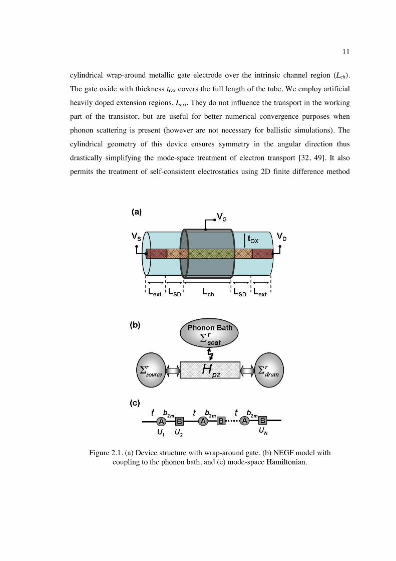
11
cylindrical wrap-around metallic gate electrode over the intrinsic channel region (Lch).
The gate oxide with thickness tOX covers the full length of the tube. We employ artificial
heavily doped extension regions, Lext. They do not influence the transport in the working
part of the transistor, but are useful for better numerical convergence purposes when
phonon scattering is present (however are not necessary for ballistic simulations). The
cylindrical geometry of this device ensures symmetry in the angular direction thus
drastically simplifying the mode-space treatment of electron transport [32, 49]. It also
permits the treatment of self-consistent electrostatics using 2D finite difference method
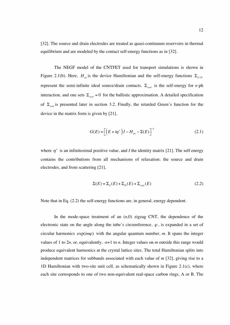
Figure 2.1. (a) Device structure with wrap-around gate, (b) NEGF model with coupling to the phonon bath, and (c) mode-space Hamiltonian.
12
[32]. The source and drain electrodes are treated as quasi-continuum reservoirs in thermal
equilibrium and are modeled by the contact self-energy functions as in [32].
The NEGF model of the CNTFET used for transport simulations is shown in
Figure 2.1(b). Here, pzH is the device Hamiltonian and the self-energy functions /S DΣ
represent the semi-infinite ideal source/drain contacts. scatΣ is the self-energy for e-ph
interaction, and one sets 0scatΣ = for the ballistic approximation. A detailed specification
of scatΣ is presented later in section 3.2. Finally, the retarded Green’s function for the
device in the matrix form is given by [21],
( )1
( ) ( )pzG E E i I H Eη−
+ = + − −Σ (2.1)
where η + is an infinitesimal positive value, and I the identity matrix [21]. The self energy
contains the contributions from all mechanisms of relaxation; the source and drain
electrodes, and from scattering [21],
( ) ( ) ( ) ( )S D scatE E E EΣ = Σ +Σ +Σ (2.2)
Note that in Eq. (2.2) the self-energy functions are, in general, energy dependent.
In the mode-space treatment of an (n,0) zigzag CNT, the dependence of the
electronic state on the angle along the tube’s circumference, ϕ , is expanded in a set of
circular harmonics exp( )imϕ with the angular quantum number, m. It spans the integer
values of 1 to 2n, or, equivalently, -n+1 to n. Integer values on m outside this range would
produce equivalent harmonics at the crystal lattice sites. The total Hamiltonian splits into
independent matrices for subbands associated with each value of m [32], giving rise to a
1D Hamiltonian with two-site unit cell, as schematically shown in Figure 2.1(c), where
each site corresponds to one of two non-equivalent real-space carbon rings, A or B. The

13
period of the zigzag tube in the longitudinal direction contains 4 such rings, ABAB, and
has length 3 cca [8], where 0.142cca nm= is the carbon-carbon bond length in graphene.
Therefore the average distance between rings is,
34
ccazΔ = . (2.3)
The diameter of the zigzag nanotube is [8],
3 cct
n adπ
= (2.4)
The mode-space transformation procedure of the real-space atomistic tight-
binding Hamiltonian is well described in [32], and is not repeated here. The two-site unit
cell, as expected, gives rise to two subbands corresponding to the conduction and the
valence band. The Hamiltonian matrix for the subbands with angular quantum number m
in an (n,0) zigzag CNT is then given by [32],
1 2
2 2
3 2
1 2
2
0
0m
m
mpz
N m
m N N N
U bb U t
t U bH
t U bb U
−
×
=
(2.5)
where 2 2 cos( / )mb t m nπ= , 3t eV≈ is the nearest neighbor hopping parameter, and N is
the total number of carbon rings along the device. Here, the diagonal elements Uj
correspond to the on-site electrostatic potential along the tube surface. All electronic
subbands in a CNT are four-fold degenerate: due to two spin states and the valley
degeneracy of two [8]. The valley degeneracy comes from the two subbands with the

14
same energy dispersion, but different m-values. Each subband can be represented as a cut
of the graphene 2D Brillouin zone by a line with a constant momentum yk . In this paper
we equate momentum with wavevector, having the dimension of inverse length. The cuts
closest to the K-points of graphene correspond to lowest-energy conduction subbands as
well as highest-energy valence subbands, and correspond in zigzag tubes to angular
momenta mL1 = round(2n/3) and mL2 = round(4n/3).
Level broadening is defined as follows and can be shown [21] to be,
†( ) ( ) ( ) ( ) ( )in outE i E E E E Γ ≡ Σ −Σ = Σ +Σ , (2.6)
where †Σ represents the Hermitean conjugate of Σ matrix defined by Eq. (2.2). Here, /in outΣ are the in/out-scattering functions (see below). The same relations apply separately
to each mechanism of relaxation. For a layered structure like the carbon nanotube, the
source self-energy function Σsource has all its entries zero except for the (1,1) element.
That is [32],
( )1, 1 0S i jΣ ≠ ≠ = (2.7)
and,
α αΣ = − −2 2(1,1)S source source t , ( )( )
α− + −
=−
2 2 21 2
12m
sourceE U t b
E U (2.8)
Similarly, ΣD has only its (N,N) element non-zero and it is given by equations similar to
(2.7) and (2.8) with U1 replaced by UN. As mentioned earlier, /S DΣ self-energies
rigorously capture the effect of semi-infinite contacts on the device. With this we can
define the in- and out-scattering functions for contact coupling,
/ / /( ) ( ) ( )in FS D S D S DE E f E EΣ = Γ − (2.9)

15
/ / /( ) ( ) 1 ( )out FS D S D S DE E f E E Σ = Γ − − (2.10)
where f(E) is the Fermi distribution, and /FS DE are the source and drain Fermi energies,
respectively. The electron and hole correlation functions are then given by [21],
†n in in inS D scatG G G = Σ +Σ +Σ (2.11)
†p out out outS D scatG G G = Σ +Σ +Σ (2.12)
where the energy dependence of the Green’s function and in/out-scattering functions is
suppressed for clarity. The in/out-scattering functions for e-ph interaction, ,in outscatΣ , are
discussed later in section 3.2. It is seen that, under ballistic conditions (i.e. , 0in outscatΣ = ), the
electron/hole distribution throughout the device is determined by the occupation of the
respective local density of states, LDOSS,D, by the corresponding reservoir Fermi
functions, ,S Df . The spectral function is [21],
( )†( ) ( ) ( ) ( ) ( )n pA E i G E G E G E G E≡ − = + (2.13)
Under ballistic conditions the spectral function can be separated into its source and drain
contributions, respectively [21];
†, ,S D S DA G G= Γ (2.14)
where the diagonal elements of ,S DA are related to the local density of states (LDOSS,D)
evolving from the corresponding contact [21]. Note that the electron and hole correlation
functions, /, ( , )n p
i jG E m , are matrices defined in the basis set of ring numbers i,j and
subbands m (we will imply the last index in the rest of the paper). Thus the diagonal

16
elements, /, ( , )n p
j jG E m , correspond to the energy density of carrier occupation at those
basis sites (single carbon ring, A or B, in a specific subband) with a given energy E. So
the total electron/hole density (per unit length) at a site zj is given by,
,
,
( , )1( )2
nj j
jm s
G E mn z dE
z π
+∞
−∞
=Δ (2.15)
,
,
( , )1( )2
pj j
jm s
G E mp z dE
z π
+∞
−∞
=Δ (2.16)
where summation is performed over the spin and subband variables, and produces the
degeneracy factor of 4 (for each non-equivalent subband). In the view of Eq. (2.13) one
recognizes that the spectral function is proportional to the density of states which is
traditionally defined [24] to include the spin summation, but is taken separately for each
subband
,1
( , )( , ) j j
D j
A E mg E z
zπ=
Δ (2.17)
Finally, the current flow from site zj to zj+1 in the nearest-neighbor tight-binding
scheme can be determined from [22, 23],
1 , 1 1, 1, , 1,
( ) ( , ) ( ) ( , )2
n nj j j j j j j j j j
m s
ie dEI H m G E m H m G E mπ
+∞
→ + + + + +
−∞
= − (2.18)
wherein the non-diagonal terms of the Hamiltonian Eq. (2.5) contain only contributions
of hopping. The above equation is a general relationship, in that it is valid even under
dissipative transport. Under ballistic conditions, however, Eq. (2.18) further simplifies
(for each non-equivalent subband) to,

17
4 ( ) ( ) ( )2
F FS D
e dEI T E f E E f E Eπ
+∞
−∞
= − − − (2.19)
with the transmission coefficient, T(E), given by,
†( ) ( ) ( ) ( ) ( )r rS DT E Trace E G E E G E = Γ Γ (2.20)
Eq. (2.19) is the famous Landauer equation widely used in mesoscopic transport [21].
One can better understand the bandstructure of carbon nanotubes in by solving for
the eigenvalues of the Hamiltonian (2.5) for zero external potential, and thereby obtaining
[32] the energy dispersion relations, ( )zE k , versus the momentum along the length of the
tube, for each subband. For the lowest conduction and the highest valence subbands,
close to the K-points the graphene band edge is approximately conic, thus [50],
2 22 =1+ z
g
E kE k
Δ
(2.21)
with the bandgap [50],
F=2vgE kΔ (2.22)
and the distance to the K-point of [50],
23 t
kd
Δ = (2.23)
The velocity of carriers in the band is [50],
z
dEvdk
=
(2.24)
Far enough from the band edge, the velocity tends to the constant value [50],
63 10 /2
ccF
a tv m s= ≈
. (2.25)

18
The 1D density of states including spin summation but only one subband (valley) can thus
be expressed as [50],
12( )( )Dg E
v Eπ=
. (2.26)
or, in other terms [50],
( )
1 22
2( )/ 2
DF
g
Eg E
v E Eπ= ⋅
−. (2.27)
2.2 Poisson’s Equation
This section summarizes the implementation of self-consistent electrostatics in
our simulation. The diagonal entries of the Hamiltonian in Eq. (2.5) contain the
electrostatic potential on the tube surface, which thereby enters the NEGF calculation of
charge distribution in Eqs. (2.15) and (2.16). On the other hand, the electrostatic potential
and the charge distribution are coupled through the Poisson’s equation as well, leading to
Figure 2.2. Self-consistency requirement between NEGF and Poisson solutions.

19
the Poisson-NEGF self-consistency requirement shown in Figure 2.2. The 2D Poisson
equation for the cylindrical transistor geometry in Figure 2.1(a) is,
( ) ( )2 ,,
r zU r z
ρ
ε∇ = − . (2.28)
Here, (r,z) is the net charge density distribution which includes dopant density as well.
At this point, it should be noted that even though Eqs. (2.15) and (2.16) give the total
carrier densities distributed throughout the whole energy range, what we really need for
determining the self-consistent potential on the tube surface, ( ),j CNT jU U r r z≡ = , is the
induced charge density ( CNTr = CNT radius). This can be determined by performing the
integrals in Eqs. (2.15) and (2.16) in a limited energy range defined with respect to the
local charge neutrality energy, EN [32, 51]. In a semiconducting CNT, due to the
symmetry of the conduction and valence bands, EN is expected to be at the mid-gap
energy. Finally, the induced charge density at site zj can be calculated from [32],
( )
, ,
( )
( ) ( )4( ) ( ) ( )2 2
N
N
E jn pj j j j
ind jE j
G E G EQ z e dE e dE
z π π
+∞
−∞
= − + + Δ
(2.29)
where the first and second terms correspond to the induced electron and hole densities,
respectively, with charge of the electron e.
Knowing the induced charge Qind, the net charge distribution (r,z) is given by,
( ) ( ),CNT j ind j D Ar r z Q z N Nρ + −= = + − (2.30)
( ), 0CNTr r zρ ≠ = (2.31)

20
where, DN + and AN − are ionized donor and acceptor concentrations, respectively. Here, it
is assumed that the induced charge and the dopants are uniformly distributed over the
CNT surface. Finally, Eq. (2.28) is solved to determine the self-consistent electrostatic
potential Uj along the tube surface. The finite difference solution scheme for the 2D
Poisson equation is further described in section 7.2.2. The calculated potential, newjU ,
gives rise to a modified Hamiltonian (Eq. (2.5)), eventually leading to the self-consistent
loop between electrostatics and quantum transport (Figure 2.2).
Even though the self-consistent procedure we have just outlined appears
conceptually straightforward, it has poor convergence properties. Therefore, a non-linear
treatment of the Poisson solution is used in practice, as explained in [22, 52], in order to
expedite the electrostatic convergence. The convergence criterion used in this process is
to monitor the maximum change in the potential profile between consecutive iterations,
i.e.: ( )max old new tolj jU U U− ≤ , where the tolerance value tolU is normally taken to be
1meV.

21
3. NEGF TREATMENT OF DISSIPATIVE TRANSPORT IN CNT
TRANSISTORS
There have been many theoretical studies on the calculation of carrier scattering
rates and mobilities in CNTs using semiclassical transport simulation based on the
Boltzmann equation [53-59]. Similarly, phonon mode calculations for CNTs are also
performed with varying degrees of complexity: continuum and force-constant models [8,
60, 61] to first-principles based methods [62-64]. The determination of electron-phonon
(e-ph) coupling strength is performed using tight-binding calculations [65-67] as well as
first-principles techniques [68]. It has been shown, however, that the influence of phonon
scattering on device performance depends not only on the phonon modes and e-ph
coupling, but also on the device geometry [34, 69]. Therefore, in order to ascertain the
impact of phonon scattering on the device performance, aforementioned calculations
should be done in the context of specific device geometry. To that end, phonon scattering
in CNT transistors has been treated using the semiclassical Boltzmann transport to
determine its effects on device characteristics [69, 70]. Semiclassical transport, however,
can fail to rigorously treat important quantum mechanical effects, such as band-to-band
tunneling, that have been deemed important in these devices [36, 38, 39], as well as the
self-consistent treatment of lifetime broadening due to scattering. Therefore, a device
simulator based on dissipative quantum transport that rigorously treats the effects of
phonon scattering will be essential for the proper assessment of CNT transistor
characteristics, and to gain a deeper understanding of carrier transport at nanoscale.
Treatment of phonon scattering in Schottky-barrier CNT transistors is described in [71,
72] where e-ph coupling is treated phenomenologically. This chapter describes the
detailed treatment of phonon scattering in CNT-MOSFETs using the NEGF formalism, as

22
well as, rigorous determination of phonon modes and their e-ph coupling in CNTs using
force-constant methods [33]. Note that this chapter is adapted from our publication [35].
3.1 Phonon Modes in a CNT
The parameters of the phonons are obviously determined by the structure of the
nanotube lattice. The one-dimensional mass density of an (n,0) nanotube is,
1C
Dm n
zρ =
Δ. (3.1)
where Cm the mass of a carbon atom, zΔ the average ring distance defined in Eq. (2.3).
The energy of a phonon of momentum q (in the unconfined dimension) is qω . The
index of the phonon subband l is implicitly combined with the momentum index here.
The half-amplitude of vibration for one phonon in a tube of length L is [24],
12q
D q
aLρ ω
= . (3.2)
For the reservoir in a thermal equilibrium at temperature T , the occupation of modes is
given by the Bose-Einstein distribution,
1
exp 1qq
B
nk Tω
−
= −
. (3.3)
As discussed earlier, the electron states in semiconducting CNTs have two-fold valley
degeneracy with the lowest-energy subbands having angular quantum numbers mL1 and
mL2. Electron-phonon scattering is governed by energy and momentum conservation
rules. Thus, as shown in Figure 3.1(a) electrons can be scattered within the same subband
23
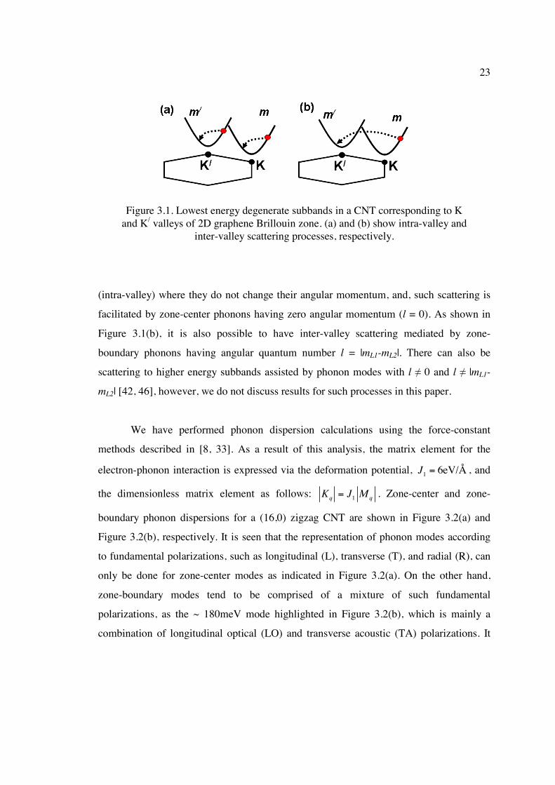
(intra-valley) where they do not change their angular momentum, and, such scattering is
facilitated by zone-center phonons having zero angular momentum (l = 0). As shown in
Figure 3.1(b), it is also possible to have inter-valley scattering mediated by zone-
boundary phonons having angular quantum number l = |mL1-mL2|. There can also be
scattering to higher energy subbands assisted by phonon modes with l 0 and l |mL1-
mL2| [42, 46], however, we do not discuss results for such processes in this paper.
We have performed phonon dispersion calculations using the force-constant
methods described in [8, 33]. As a result of this analysis, the matrix element for the
electron-phonon interaction is expressed via the deformation potential, 1 6eV/ÅJ = , and
the dimensionless matrix element as follows: 1q qK J M= . Zone-center and zone-
boundary phonon dispersions for a (16,0) zigzag CNT are shown in Figure 3.2(a) and
Figure 3.2(b), respectively. It is seen that the representation of phonon modes according
to fundamental polarizations, such as longitudinal (L), transverse (T), and radial (R), can
only be done for zone-center modes as indicated in Figure 3.2(a). On the other hand,
zone-boundary modes tend to be comprised of a mixture of such fundamental
polarizations, as the ~ 180meV mode highlighted in Figure 3.2(b), which is mainly a
combination of longitudinal optical (LO) and transverse acoustic (TA) polarizations. It
Figure 3.1. Lowest energy degenerate subbands in a CNT corresponding to K and K/ valleys of 2D graphene Brillouin zone. (a) and (b) show intra-valley and
inter-valley scattering processes, respectively.

24
should also be noted that the frequency of the radial breathing mode (RBM) calculated
here is in very good agreement with the relationship derived from ab initio calculations,
28 /RBM tmeV dω ≈ (3.4)
where dt is the CNT diameter in nanometers [62, 63, 73]. The Hamiltonian of electron-
phonon interaction in a general form is [24],
Figure 3.2. Energy dispersion for phonon modes in a (16,0) CNT: (a) zone-center phonons that allow intra-valley scattering and, (b) zone-boundary phonons that allow inter-valley scattering. Modes that effectively couple to the electrons are indicated by dashed circles.
Zone-boundary phonons are composed of a mixture of fundamental polarizations.
25
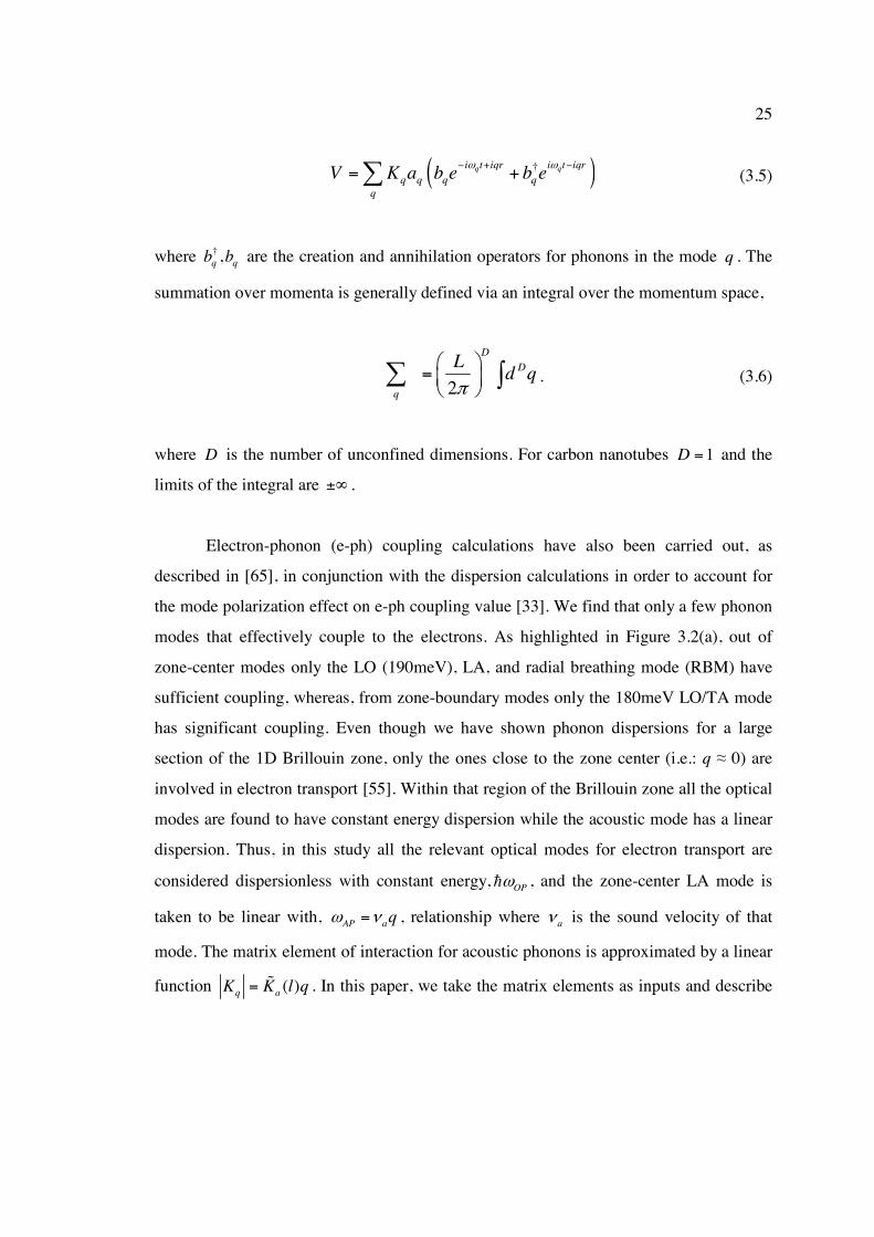
( )†q qi t iqr i t iqrq q q q
qV K a b e b eω ω− + −= + (3.5)
where † ,q qb b are the creation and annihilation operators for phonons in the mode q . The
summation over momenta is generally defined via an integral over the momentum space,
2
DD
q
L d qπ
=
. (3.6)
where D is the number of unconfined dimensions. For carbon nanotubes 1D = and the
limits of the integral are ±∞ .
Electron-phonon (e-ph) coupling calculations have also been carried out, as
described in [65], in conjunction with the dispersion calculations in order to account for
the mode polarization effect on e-ph coupling value [33]. We find that only a few phonon
modes that effectively couple to the electrons. As highlighted in Figure 3.2(a), out of
zone-center modes only the LO (190meV), LA, and radial breathing mode (RBM) have
sufficient coupling, whereas, from zone-boundary modes only the 180meV LO/TA mode
has significant coupling. Even though we have shown phonon dispersions for a large
section of the 1D Brillouin zone, only the ones close to the zone center (i.e.: q 0) are
involved in electron transport [55]. Within that region of the Brillouin zone all the optical
modes are found to have constant energy dispersion while the acoustic mode has a linear
dispersion. Thus, in this study all the relevant optical modes for electron transport are
considered dispersionless with constant energy, OPω , and the zone-center LA mode is
taken to be linear with, AP aqω ν= , relationship where aν is the sound velocity of that
mode. The matrix element of interaction for acoustic phonons is approximated by a linear
function ( )q aK K l q= . In this paper, we take the matrix elements as inputs and describe

26
the general method of treatment of electron-phonon interaction in nanotubes for both
optical and acoustic phonon modes.
3.2 Electron-Phonon Scattering
The e-ph scattering is treated within the self-consistent Born approximation
(SCBA) [20], in that, the Green’s function G(E) in eq. (2.1) and the scattering self-energy
( )scat EΣ in eq. (2.2) have to be determined self-consistently. NEGF formulation of carrier
scattering due to optical and acoustic phonons is described in this section. Section 3.3
discusses the numerical implementation of the SCBA approach. The in/out-scattering
functions for optical phonon scattering of electrons in a ring i from subband 'm to
subband m are [21],
0 0( , , , ) ( 1) ( , , ', ) ( , , ', )in n nscat i i m E D n G i i m E D n G i i m Eω ωω ωΣ = + + + − (3.7)
0 0( , , , ) ( 1) ( , , ', ) ( , , ', )out p pscat i i m E D n G i i m E D n G i i m Eω ωω ωΣ = + − + + . (3.8)
Here, we have used the local interaction approximation in writing the in/out-scattering
functions by assuming them to be diagonal [22]. In eqs. (3.7) and (3.8) the first term on
the right hand side corresponds to phonon emission mediated processes while the second
term to that of phonon absorption. The imaginary part of the self-energy, related to the
level broadening is now given by [21],
( ) ( ) ( ) ( )2 2
i in outscat scat scat scat
i iE E E E Σ = − Γ = − Σ + Σ . (3.9)
The real part of self-energy is manifested as a shift of energy levels and is computed by
using the Hilbert transform [21],

27
( ')'P2 '
r scatscat
EdEE EπΓ
Σ =− . (3.10)
In this work we neglect the real part of e-ph self-energy in order to simplify the
computations and because the estimates suggest small influence of the real part. For
optical phonon scattering, the coupling constant D0 is [33],
2
00
1 02 D
KD
zρ ω=
Δ
. (3.11)
For elastic scattering, i.e. in case it is possible to neglect the energy of a phonon,
the in/out-scattering functions are [21],
( , , , ) ( , , ', )in nscat eli i m E D G i i m EΣ = . (3.12)
( , , , ) ( , , ', )out pscat eli i m E D G i i m EΣ = . (3.13)
In this case there is no need to neglect the real part of self-energy, and its complete
expression is,
( , , , ) ( , , ', )scat eli i m E D G i i m EΣ = . (3.14)
For acoustic phonon scattering, the coupling constant is [33],
2
21
a Bel
D a
K k TDv zρ
=Δ
. (3.15)
28
3.3 Numerical Treatment of Dissipative Transport
Here, we summarize the overall simulation procedure used in this study.
Throughout this work we encounter many energy integrals such as Eqs. (2.18) and (2.29).
The use of a uniform energy grid becomes prohibitive when sharp features such as
quantized energy states need to be accurately resolved. Therefore, an adaptive technique
for energy integrations is used based on the quad.m subroutine of Matlab® programming
language. The treatment of phonon scattering is performed using the self-consistent Born
approximation [22, 23]. In that, we need to treat the interdependence of the device
Green’s function, Eq. (2.1), and the scattering self-energy, Eq. (2.2), self-consistently.
The treatment of OP scattering is presented first, followed by that for AP scattering.
3.3.1 Treatment of optical phonon scattering
The determination of in/out-scattering functions, Eqs. (3.7) and (3.8), for OP
scattering requires the knowledge of the electron and hole correlation functions;
specifically, the energy-resolved diagonal elements of these functions, ( )/,
n pj jG E . It
should be noted that only the diagonal elements are needed since we take the scattering
self-energy functions to be diagonal in the local interaction approximation [22, 23]. With
that, we use the following procedure to determine G(E) and ( )scat EΣ self-consistently.
1) Start with known energy-resolved /,
n pj jG distributions. Ballistic distributions are
used as the starting point.
2) Determine ( )inscat EΣ , ( )out
scat EΣ , and ( )scat EΣ using Eqs. (3.7), (3.8), and (3.9),
respectively, at a given energy E.
3) Determine new G(E) using Eq. (2.1).
4) Now, determine new Gn(E) and Gp(E) from Eqs. (2.11) and (2.12), respectively.
5) Repeat steps 2 through 4 for all energies and build new /,
n pj jG distributions.

29
6) Repeat steps 1 through 5 until convergence criterion is satisfied. We use the
convergence of the induced carrier density, Eq. (2.29), as the criterion.
In the above calculations, there is a repetitive need for the inversion of a large
matrix, Eq. (2.1), which can be a computationally prohibitive task. However, we only
need a few diagonals of the eventual solution such as the main diagonal of Gn/p for the
calculation of scattering and carrier densities, and the upper/lower diagonals of Gn for the
calculation of current in Eq. (2.18). The determination of these specific diagonals, in the
nearest-neighbor tight-binding scheme, can be performed using the efficient algorithms
given in [74]. A Matlab® implementation of these algorithms can be found at
https://www.nanohub.org/resources/1983/. Finally, it should be noted that the overall
accuracy of the Born convergence procedure described above is confirmed at the end by
observing the current continuity throughout the device, Eq. (2.18).
3.3.2 Treatment of acoustic phonon scattering
Similar to the above method, AP scattering is treated using the following
procedure,
1) Start with known energy-resolved /,
n pj jG distributions. Ballistic distributions are
used as the starting point.
2) Determine ( )inscat EΣ , ( )out
scat EΣ , and ( )scat EΣ using Eqs. (3.12), (3.13), and (3.9),
respectively, at a given energy E.
3) Determine new G(E) using Eq. (2.1).
4) Now, determine new Gn(E) and Gp(E) at energy E from Eqs. (2.11) and (2.12),
respectively.
5) Repeat steps 2 through 4 until convergence criterion is satisfied. Here, we use the
convergence of Gn(E).
6) Repeat steps 2 thru 5 for all energies and build new /,
n pj jG distributions.
30
7) Repeat steps 1 through 6 until convergence criterion is satisfied. We use the
convergence of the induced carrier density, Eq. (2.29), as the criterion.
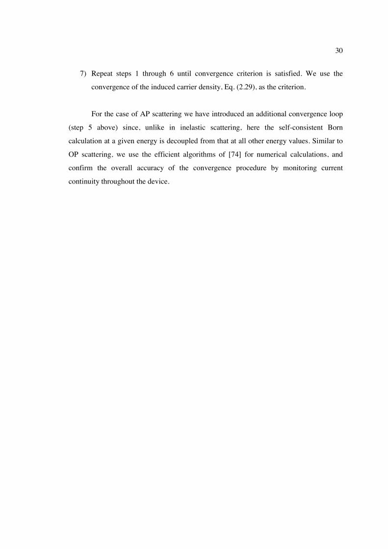
For the case of AP scattering we have introduced an additional convergence loop
(step 5 above) since, unlike in inelastic scattering, here the self-consistent Born
calculation at a given energy is decoupled from that at all other energy values. Similar to
OP scattering, we use the efficient algorithms of [74] for numerical calculations, and
confirm the overall accuracy of the convergence procedure by monitoring current
continuity throughout the device.

31
4. EFFECT OF PHONON SCATTERING IN CNT-MOSFETS
This chapter presents the simulation results for transport in CNTFETs using the
NEGF formalism described in the ealier chapters. Here, we explore two specific
examples: 1) the convetional operation of a CNT-MOSFET wherein the carrier transport
is due to termionic injection over the channel barrier, 2) Band-to-band tunneling transport
in a CNT-MOSFET where conduction is mainly due to carrier tunneling through the
quantized conduction band states in a p-type MOSFET at large positive gate biases. It
should be noted that section 4.1 is adapted from our publication [35], and, section 4.2 is
adapted from [38].
4.1 Effect of Phonon Scattering on Conventional Operation of CNT-MOSFETs
Dissipative transport simulations are carried out as explained in the previous
chapters, and the results are compared to that with ballistic transport. Here, we first study
the effects of phonon scattering on CNTFET characteristics using a (16,0) tube as a
representative case. Then, we compare the diameter dependence using (16,0), (19,0) and
(22,0) tubes, that belong to the mod(n-m,3) = 1 family. The device parameters (Figure 2.1
(a)) used for the simulation of OP scattering are as follows: Lch = 20nm, LSD = 30nm, Lext
= 0, tox = 2nm (HfO2 with = 16), and the source/drain doping NSD = 1.5/nm. This doping
concentration should be compared with the carbon atom density of (4n/3acc) in an (n,0)
zigzag CNT, which is ~ 150/nm in a (16,0) tube. For the simulation of AP scattering, a
heavy doped extension region is used for better convergence of the self-consistent
electrostatic solution. In this case, LSD = 20nm, Lext = 15nm, NSD = 1.5/nm, and the
extension doping, Next = 1.8/nm are used; and all the other parameters are same as for the

32
previous case. Except for assisting in the convergence procedure, the effect of the heavy
doped extensions on the device characteristics is negligible. It should be noted that under
OP scattering we consider the impact of intra-LO, intra-RBM, and inter-LO/TA phonon
modes all together simultaneously (Table 4-1). The intra-LA mode is treated under AP
scattering separately.
Table 4-1. Phonon energy and e-ph coupling parameters for the CNTs used in this study
Phonon mode
(16,0)
d = 1.25nm,
EG =0.67eV
(19,0)
d = 1.50nm,
EG =0.56eV
(22,0)
d = 1.70nm,
EG =0.49eV
Intra LO
(190meV)a 9.80x10⁻³ eV2 8.19x10⁻³ eV2 7.00x10⁻³ eV2
Intra RBMa,b 0.54x10⁻³ eV2
(21meV)
0.36x10⁻³ eV2
(18meV)
0.25x10⁻³ eV2
(16meV)
Inter LO/TA
(180meV)a 19.30x10⁻³ eV2 16.26x10⁻³ eV2 14.13x10⁻³ eV2
Intra LAc 2.38x10⁻³ eV2 2.00x10⁻³ eV2 1.73x10⁻³ eV2
a) e-ph coupling for optical phonons is determined according to Eq (3.11);
b) RBM energy is diameter dependent, and shown in the parentheses;
c) e-ph coupling for acoustic phonons is determined according to Eq. (3.15).

33
Figure 4.1 compares the IDS-VDS results for the (16,0) CNTFET under ballistic
transport and that with OP and AP scattering. It is seen that phonon scattering can indeed
have an appreciable effect on the device ON-current: at VGS = 0.6V the ON-current is
reduced by ~ 9% and ~ 7% due to OP and AP scattering, respectively. The relative
importance of the two scattering mechanisms also shows an interesting behavior. Up to
moderate gate biases the effect of AP scattering is stronger (VGS 0.5V). At large gate
biases OP scattering becomes the more important process (VGS 0.6V). This relative
behavior can be better observed in the IDS-VGS results shown in Figure 4.2. Here, it is seen
that up to moderate gate biases AP scattering causes a larger reduction in the device
current compared to OP scattering. Furthermore, the current reduction seen in this case
for OP scattering is mainly due to the low-energy RBM mode [34]. At large gate biases,
however, the effect of OP scattering becomes stronger, reducing the current by ~ 16%
from the ballistic level at VGS = 0.7V. Previous studies have shown that the strong current
degradation at larger gate biases is due to high-energy OP scattering processes becoming
Figure 4.1. IDS-VDS for the (16,0) CNTFET under ballistic transport, OP scattering (all modes together), and AP scattering. High-energy OP scattering becomes important at
sufficiently large gate biases. Until then AP and RBM scattering are dominant.

34
effective (mainly inter-LO/TA and intra-LO modes) [58, 59]. Nevertheless, the
importance of AP and low-energy RBM scattering should be appreciated since these
might be the relevant scattering mechanisms under typical biasing conditions of a
nanoscale transistor [75].
The relative behavior of OP and AP scattering can be understood by studying
Figure 4.3. It shows the energy-position resolved current spectrum, which is essentially
the integrand of Eq. (2.18), under ballistic transport and OP scattering. In Figure 4.3(a), it
is seen that under ballistic conditions, carriers injected from the source reaches the drain
without losing energy inside the device region. There exists a finite density of current
below the conduction band edge (EC) which is due to quantum mechanical tunneling. In
the presence of OP scattering, however, it is seen that the carriers near the drain end
relaxes to low energy states by emitting phonons (Figure 4.3(b)). Nevertheless, up to
moderate gate biases high-energy OP scattering does not affect the device current due to
the following reason. For such biasing conditions the energy difference between the
Figure 4.2. IDS-VGS for the (16,0) CNTFET at VDS = 0.3V under ballistic transport, OP scattering (all modes together), and AP scattering. The inset shows that acoustic
phonons are more detrimental up to moderate gate biases.

35
source Fermi level and the top of the channel barrier, FSη , is smaller than the optical
phonon energy: FS OPη ω . Therefore, a majority of the positive going carriers (source
drain) in the channel region does not experience high-energy OP scattering, except for
a minute portion in the high-energy tail of the source Fermi distribution.
On the other hand, when these carriers reach the drain end there are empty low-
lying states that they scatter to. After emitting a high-energy OP, however, these carriers
Figure 4.3. Energy-position resolved current spectrum for (16,0) CNTFET at VGS = 0.5V, VDS = 0.5V (logarithmic scale). (a) ballistic, (b) dissipative transport (all OP
modes together). Thermalization near the drain end by emitting high-energy OPs leaves the electrons without enough energy to overcome the channel barrier.

36
do not have enough energy to surmount the channel barrier and reach the source region
again. Thus, the effect of high-energy OP scattering on the device current is suppressed
until backscattering becomes effective at larger gate biases for FS OPη ω≥ . On the other
hand, low-energy RBM phonons and acoustic phonons can effectively backscatter at all
gate biases. They are the dominant scattering mechanism until high-energy OP becomes
important at large biases [34, 69].
Figure 4.4 shows the energy-position resolved electron density spectrum, which is
essentially the integrand of Eq. (2.15). Examining Figure 4.4(a), one can see that
electrons are filled up to the respective Fermi levels in the two contact regions. In these
regions, a characteristic interference pattern in the distribution function is observed due to
quantum mechanical inference of positive and negative going states [32]. Quantized
valence band states in the channel region are due to the longitudinal confinement in this
effective potential well [32]. In the presence of OP scattering, a few interesting features
are observed in Figure 4.4(b). The interference pattern seen in the contact regions are
smeared due to the broadening of energy states by incoherent OP scattering. The electrons
near the drain end relax down to low lying empty states, even though they are less
discernible in the linear color scale employed here. More interestingly, now we observe a
multitude of quantized valence band states in the channel region. Such states with
energies below the conduction band edge of the drain region are observed here due to
their additional broadening by coupling to the phonon bath. They were unobservable in
the ballistic case since they lied inside the bandgap regions of the contact reservoirs that
led to zero contact broadening, / 0S DΓ ≈ . The additional low-intensity states observed are
the phonon induced side-bands of the main quantized levels originating from the variety
of OP modes considered here. Carrier transport through these quantized states is indeed
possible under appropriate biasing conditions, and lead to many interesting properties
such as, less than 60mV/decade subthreshold operation and, phonon-assisted inelastic
tunneling [36, 38]. This regime of device operation will be discussed in the next section.
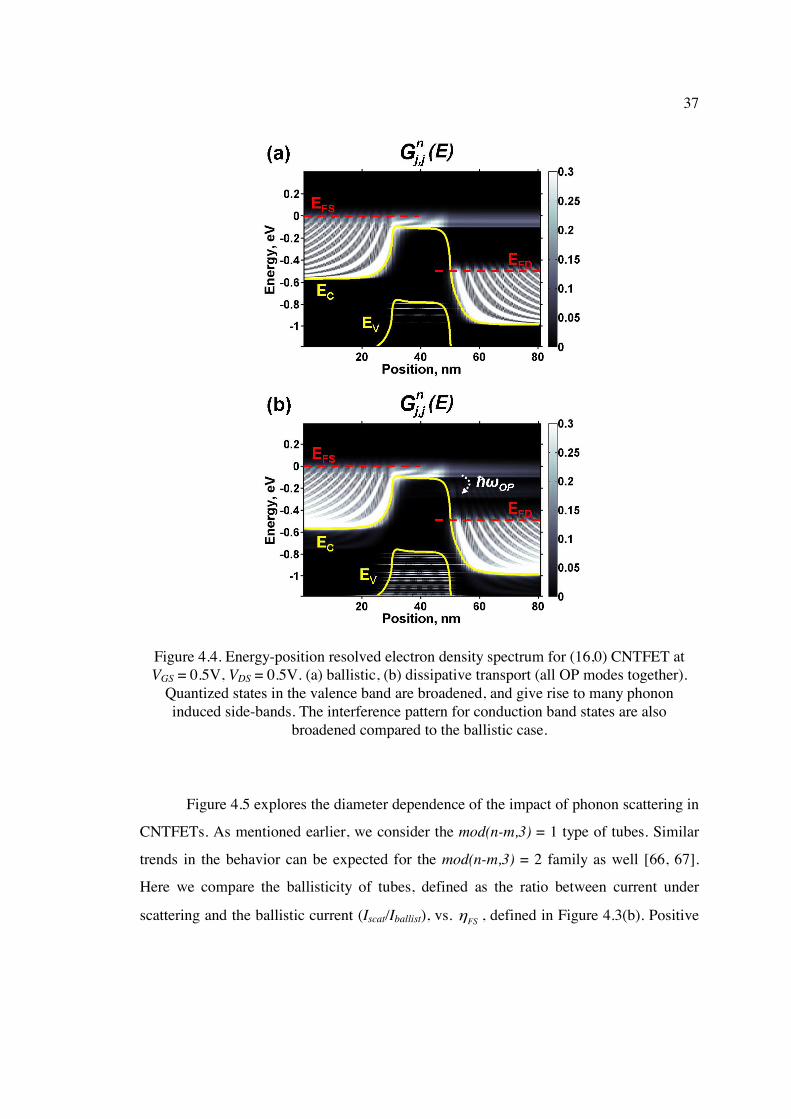
37
Figure 4.5 explores the diameter dependence of the impact of phonon scattering in
CNTFETs. As mentioned earlier, we consider the mod(n-m,3) = 1 type of tubes. Similar
trends in the behavior can be expected for the mod(n-m,3) = 2 family as well [66, 67].
Here we compare the ballisticity of tubes, defined as the ratio between current under
scattering and the ballistic current (Iscat/Iballist), vs. FSη , defined in Figure 4.3(b). Positive
Figure 4.4. Energy-position resolved electron density spectrum for (16,0) CNTFET at VGS = 0.5V, VDS = 0.5V. (a) ballistic, (b) dissipative transport (all OP modes together).
Quantized states in the valence band are broadened, and give rise to many phonon induced side-bands. The interference pattern for conduction band states are also
broadened compared to the ballistic case.

38
FSη corresponds to the on-state of the device at large positive gate biases, and negative
FSη is for the off-state. The characteristic roll-off of ballisticity under OP scattering is
seen in Figure 4.5(a) [34]. In that, the roll-off is due to high-energy OP scattering
becoming effective at large gate biases. The ballisticity reduction at small gate biases is
due to the low-energy RBM scattering [34].
In Figure 4.5(a) it is seen that the impact of high-energy OP scattering decreases
Figure 4.5. Ballisticity (Iscat/Iballist) vs. FSη for (16,0), (19,0) and (22,0) CNTFETs, (a) with all OP modes together, (b) with AP scattering. FSη is defined as the energy
difference between the source Fermi level and the channel barrier (see Figure 4.3(b)).

39
for larger diameter tubes. This can be easily understood by noting that the e-ph coupling
parameter for these modes (intra-LO and inter-LO/TA) monotonically decreases with
increasing diameter (Table 4-1). On the other hand, the impact of the RBM mode at low
gate biases seems to be nearly diameter independent for the tubes considered here, even
though there is a similar decrease in e-ph coupling for larger diameter tubes (Table 4-1).
This behavior is due to the concomitant reduction of energy of the RBM mode at larger
diameters that leads to an increased amount of scattering events, which ultimately cancels
out the overall impact on device current.
Diameter dependence of AP scattering is shown in Figure 4.5(b). The ballisticity
for larger tubes is higher due to the corresponding reduction of the e-ph coupling
parameter shown in Table 4-1. They all show a slight increase in the ballisticity at larger
gate biases due to majority of the positive going carriers occupying states well above the
channel conduction band edge [34]. The backscattering rate is a maximum near the band
edge due to increased 1D density of states and decays at larger energies [53, 55, 57]. It is
seen that for all the tubes on Figure 4.5, the impact of AP scattering is stronger compared
to OP scattering until the high-energy modes become effective. Under typical biasing
conditions for nanoscale transistor operation, FSη will be limited ( FSη 0.15eV) and the
transport will be dominated by AP and low-energy RBM scattering [75].
4.2 Phonon-Assisted Inelastic Tunneling in CNT-MOSFETs
Device power dissipation has become a major challenge for the continued scaling
of integrated circuits [1, 76]. One important factor contributing to the overall power
dissipation is poor sub-threshold (off-state) properties of modern transistors. This has led
to large sub-threshold leakage currents, and it has limited the ability to scale the power
supply voltage (VDD), which has been the preferred way to decrease power dissipation in
modern integrated circuits [76]. The sub-threshold swing (S) for conventional transistors,
which determines how effectively the transistor can be turned off by changing the gate

40
voltage (IDS vs. VGS), has a fundamental limit of 2.3 /BS k T q= × mV/decade 60mV/dec
at room temperature, where kB is the Boltzmann constant, T the temperature, and q the
electron charge [77]. The need to maintain a certain ratio of on-current to off-current
limits scaling of the power supply voltage, aggravating heat dissipation problems in
modern high-performance circuits.
The aforementioned limitations on the off-state performance of conventional
transistors equally apply to those based on carbon nanotubes (CNTs): both Schottky-
barrier transistors (SB-CNTFETs) and metal-oxide-semiconductor field-effect transistors
(CNT-MOSFETs) with doped source/drain contacts [78-81]. It has been experimentally
observed that carrier transport in CNTs can be nearly ballistic [47, 48, 82]. High-
performance CNT transistors operating close to the ballistic limit have also been
demonstrated [13-15]. Recently, p-type CNT-MOSFETs with near ideal gate control and
sub-threshold operation close to the fundamental limit of S 60mV/dec at negative gate
voltages (VGS) have been reported [41, 42]. At positive voltages, these CNT-MOSFETs
begin to turn on again with a swing of 40~50mV/dec which is smaller than the
conventional limit of 60mV/dec. This regime of operation is attributed to band-to-band
tunneling (BTBT) [36, 41], and should be distinguished from the ambipolar operation in
SB-CNTFETs where the ambipolar branch is due to opposite type of carrier injection
(electrons in the case of p-type FETs) from the drain Schottky contact [80, 83].
Specialized device geometries including that based on BTBT have been actively
investigated to obtain improved sub-threshold performance in CNT-MOSFET transistors
[37, 84]. Here we present detailed theoretical simulations for the BTBT operation of
CNT-MOSFETs using the NEGF formalism described earlier for both ballistic and
dissipative quantum transport. Comparing these results with the recently reported data in
Ref. [42], we provide compelling evidence that the BTBT operation of CNT-MOSFETs
is strongly affected by phonon-assisted tunneling.

41
The idealized device structure used in this study, shown in Figure 2.1 (a), is a p-
type CNT-MOSFET with wrap-around high-k (HfO2 ~ = 25) gate dielectric with
thickness tOX = 2nm, p-doped source/drain regions (NS/D = 0.6/nm) with LSD = 40nm, Lext
= 0, and an intrinsic channel length of Lch = 30nm. A zigzag (16,0) CNT with diameter ~
1.2nm and bandgap ~ 0.7eV is considered. The CNT-metal contacts at the ends of
source/drain regions are assumed to be Ohmic, with perfect transparency for carrier
transport. In experimental devices the Ohmic contacts with electrostatically induced
doping is achieved through a back-gated geometry [41, 42, 85]. Although the device
structure is idealized, the device parameters are in agreement with those in Ref. [42]. Our
simulations are performed for p-type CNT-MOSFETs in correspondence with
experiments [42]. Due to the symmetry of conduction and valence bands in CNTs [8], the
simulated I-V curves for n-type and p-type transistors are expected to coincide after
reversing the polarity of voltages; and indeed we have verified this equivalence.
The NEGF calculations for dissipative transport are performed self-consistently
with electrostatic simulations as described in previous chapters. We use the nearest
neighbor pz tight-binding Hamiltonian (zp TBH − ) to describe the CNT electronic structure
[8, 21]. The simulations are carried out in the mode-space, considering transport through
the first conduction and valence subbands (EC1 and EV1), respectively [49]. The difference
of energy to the next highest subbands, i.e. |EC2-EC1| = |EV2-EV1|, is about 370meV so the
transport through higher subbands can be neglected for typical biasing conditions.
In this study we include both one-phonon and two-phonon scattering processes in
our simulation. For the (16,0) CNT and the longitudinal optical (LO) phonon mode
considered in here, OPω = 195meV and ROP = 0.01eV2, respectively (Table 4-1). Two-
phonon scattering is included similarly, with the phonon energy replaced by 2-ph =
360meV, corresponding to 180meV zone-boundary optical phonons, and the coupling
parameter related to that of the one-phonon transition via [86],

42
22
2( )( / 2)
OPe ph OP
tot ph
R E RE ω−
Γ=
Γ ± , (4.1)
where OPΓ is the one-phonon broadening and totΓ is the total broadening due to
scattering and the source/drain reservoirs defined in Eqs. (2.6) and (3.9).
We have performed self-consistent NEGF calculations for both ballistic
( 0scatΣ = ) and dissipative ( 0scatΣ ≠ ) transport using the efficient numerical algorithms
reported in Ref. [74]. The simulation results are compared against the data reported in
Ref. [42]; the relevant experimental IDS-VGS plot is reproduced in Figure 4.6 for the sake
of completeness. In examining Figure 4.6 we can observe a few important features of the
p-type CNT-MOSFET operation: 1) near ideal (S 60mV/dec) sub-threshold behavior
under conventional MOSFET operation for negative VGS biases, 2) larger on-currents for
the conventional operation compared to BTBT regime, 3) S 50mV/dec (< 60mV/dec
conventional limit) is observed for BTBT transport at VDS = -0.01V. The BTBT sub-
threshold swing, however, degrades with increasing VDS biases. 4) The onset of BTBT
occurs at a smaller VGS with increasing VDS, i.e., the onset VGS bias point moves left on
Figure 4.6. Experimental IDS-VGS data at different VDS biases for the p-type CNT-MOSFET; reproduced from Ref. [42].

43
Figure 4.6 with increasing VDS. Similar experimental characteristics for BTBT operation
in p-type CNT-MOSFETs have also been observed by J. Appenzeller et al. at IBM T. J.
Watson Research Center (personal communication). These experimental device
characteristics will be compared against our computational results in order to elucidate
the transport mechanisms.
Ref. [36] presents a detailed study of the BTBT operation in a CNT-MOSFET,
and here we summarize the transport mechanism responsible for it. Figure 4.7 (a) and (b)
depict the two main mechanisms for BTBT transport in p-type CNT-MOSFETs with
sufficiently short channel lengths. For such devices, due to longitudinal confinement
Figure 4.7. BTBT operation in a p-type CNT-MOSFET: (a) For large positive VGS, direct tunneling of electrons from drain to source through the quantized conduction band states in the channel region, (b) For moderately positive VGS direct tunneling is prohibited, but
inelastic tunneling is possible in the presence of optical phonons (dashed arrows), (c) NEGF simulation results for energy-position resolved current density spectrum
(logarithmic scale) under 195meV LO phonon scattering at VGS = 0.4V, VDS = -0.3V.
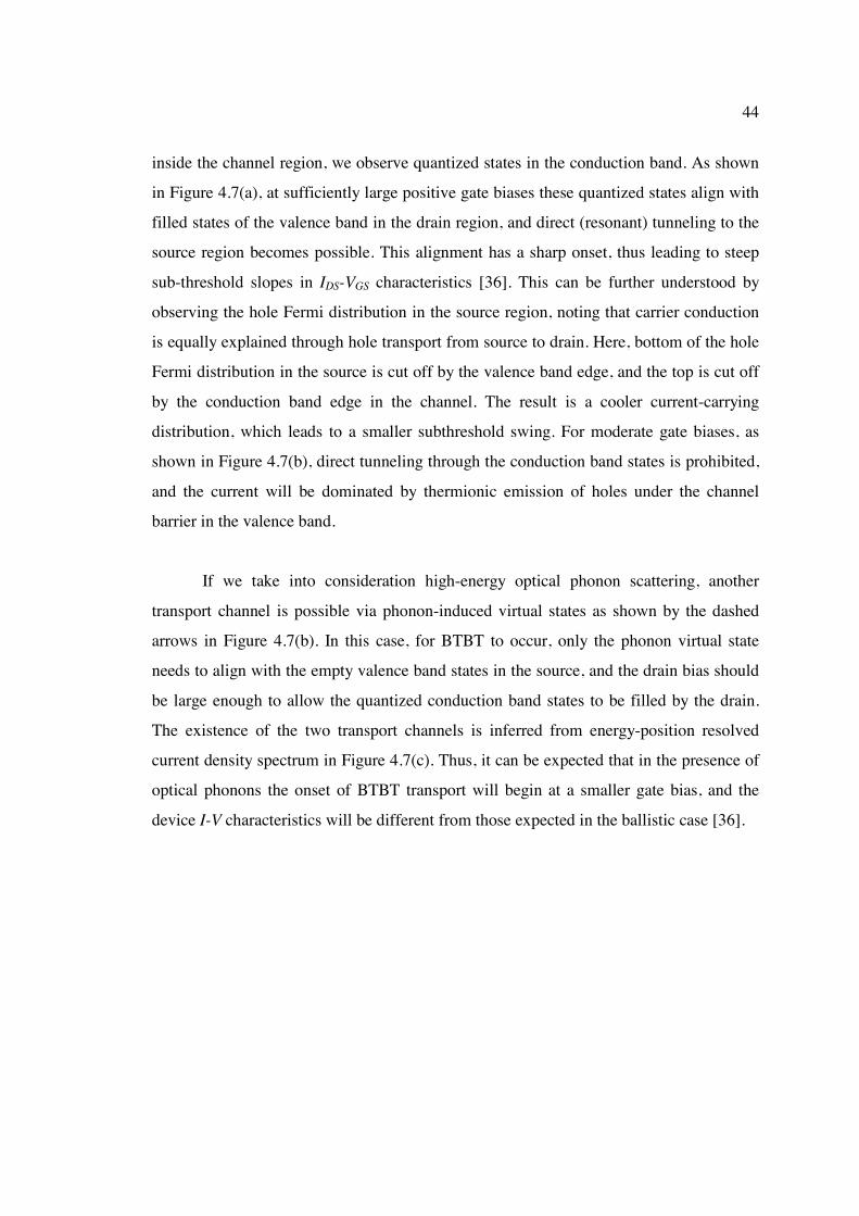
44
inside the channel region, we observe quantized states in the conduction band. As shown
in Figure 4.7(a), at sufficiently large positive gate biases these quantized states align with
filled states of the valence band in the drain region, and direct (resonant) tunneling to the
source region becomes possible. This alignment has a sharp onset, thus leading to steep
sub-threshold slopes in IDS-VGS characteristics [36]. This can be further understood by
observing the hole Fermi distribution in the source region, noting that carrier conduction
is equally explained through hole transport from source to drain. Here, bottom of the hole
Fermi distribution in the source is cut off by the valence band edge, and the top is cut off
by the conduction band edge in the channel. The result is a cooler current-carrying
distribution, which leads to a smaller subthreshold swing. For moderate gate biases, as
shown in Figure 4.7(b), direct tunneling through the conduction band states is prohibited,
and the current will be dominated by thermionic emission of holes under the channel
barrier in the valence band.
If we take into consideration high-energy optical phonon scattering, another
transport channel is possible via phonon-induced virtual states as shown by the dashed
arrows in Figure 4.7(b). In this case, for BTBT to occur, only the phonon virtual state
needs to align with the empty valence band states in the source, and the drain bias should
be large enough to allow the quantized conduction band states to be filled by the drain.
The existence of the two transport channels is inferred from energy-position resolved
current density spectrum in Figure 4.7(c). Thus, it can be expected that in the presence of
optical phonons the onset of BTBT transport will begin at a smaller gate bias, and the
device I-V characteristics will be different from those expected in the ballistic case [36].

45
Figure 4.8 (a) shows the simulated IDS-VGS characteristics under ballistic transport
for the p-type CNT-MOSFET studied here. It is seen that the sub-threshold swing for
regular MOSFET operation (negative VGS for p-type devices) is indeed at the theoretical
limit of 60mV/dec, which is not surprising given the wrap-around gate geometry we have
employed in our simulations. The on-current for regular operation is also larger than that
for the BTBT operation. The overall device currents observed in our simulator, however,
are larger than the experimental ones, which can be attributed to contact resistance in the
experiment. The simulated sub-threshold swing in the BTBT regime is S 20mV/dec at
VDS = -0.01V. Under ballistic transport, the steep slope for BTBT regime does not
degrade for large VDS, contrary to the experimental results in Figure 4.6. More
Figure 4.8. Simulated IDS-VGS characteristics for the p-type CNT-MOSFET (black solid line - 60mV/dec swing): (a) ballistic, (b) one-phonon scattering with 195meV LO
mode.
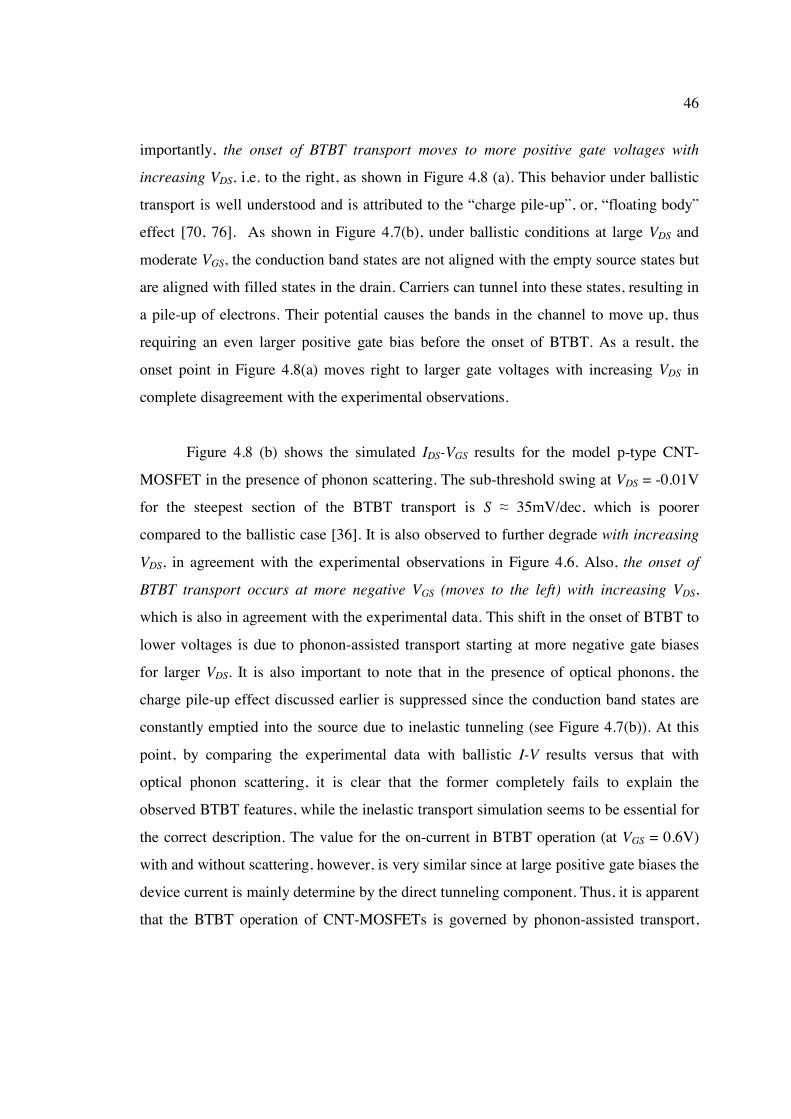
46
importantly, the onset of BTBT transport moves to more positive gate voltages with
increasing VDS, i.e. to the right, as shown in Figure 4.8 (a). This behavior under ballistic
transport is well understood and is attributed to the “charge pile-up”, or, “floating body”
effect [70, 76]. As shown in Figure 4.7(b), under ballistic conditions at large VDS and
moderate VGS, the conduction band states are not aligned with the empty source states but
are aligned with filled states in the drain. Carriers can tunnel into these states, resulting in
a pile-up of electrons. Their potential causes the bands in the channel to move up, thus
requiring an even larger positive gate bias before the onset of BTBT. As a result, the
onset point in Figure 4.8(a) moves right to larger gate voltages with increasing VDS in
complete disagreement with the experimental observations.
Figure 4.8 (b) shows the simulated IDS-VGS results for the model p-type CNT-
MOSFET in the presence of phonon scattering. The sub-threshold swing at VDS = -0.01V
for the steepest section of the BTBT transport is S 35mV/dec, which is poorer
compared to the ballistic case [36]. It is also observed to further degrade with increasing
VDS, in agreement with the experimental observations in Figure 4.6. Also, the onset of
BTBT transport occurs at more negative VGS (moves to the left) with increasing VDS,
which is also in agreement with the experimental data. This shift in the onset of BTBT to
lower voltages is due to phonon-assisted transport starting at more negative gate biases
for larger VDS. It is also important to note that in the presence of optical phonons, the
charge pile-up effect discussed earlier is suppressed since the conduction band states are
constantly emptied into the source due to inelastic tunneling (see Figure 4.7(b)). At this
point, by comparing the experimental data with ballistic I-V results versus that with
optical phonon scattering, it is clear that the former completely fails to explain the
observed BTBT features, while the inelastic transport simulation seems to be essential for
the correct description. The value for the on-current in BTBT operation (at VGS = 0.6V)
with and without scattering, however, is very similar since at large positive gate biases the
device current is mainly determine by the direct tunneling component. Thus, it is apparent
that the BTBT operation of CNT-MOSFETs is governed by phonon-assisted transport,

47
and dominates the sub-threshold characteristics in this regime. At this point it should be
noted that elastic scattering due to acoustic phonons is not expected to affect the BTBT
sub-threshold swing which is mainly determined by the inelastic tunneling due to optical
phonons. The saturation current in the BTBT regime, however, can be reduced by
acoustic phonon back-scattering when such events become allowed by energy
conservation. It should also be pointed out that our simulations show slight reduction of
the BTBT on-current at large gate biases, VGS > 0.6V. This reduction is, however, smaller
than that seen in Figure 4.6 at low drain biases.
The device operation under large drain biases is discussed next. The solid-triangle
curve of Figure 4.9 shows the IDS-VGS relationship for the model p-type CNT-MOSFET at
VDS = -0.6V under 195meV LO phonon scattering. It is seen that, due to the charge pile-
up effect at such a high drain bias, the onset of BTBT is pushed to larger positive voltages
(right). On the other hand, Figure 4.6 indicates that the experimentally observed onset of
BTBT does not show such effects at large drain biases, and may move further left to
smaller gate voltages. Examining Figure 4.7 (b), it is clear that the onset of BTBT can be
Figure 4.9. Simulated IDS-VGS with only one-phonon scattering due to 195meV zone center LO mode (solid lines) and, also including two-phonon scattering due to 2 x
180meV zone-boundary mode (dashed lines). Red-star, blue-circle, and green-square curves are at the same voltages as in Figure 4.8 (b), magenta-triangle curves are at VDS =
-0.6V.

48
moved left to smaller gate biases if there are higher energy optical phonons that could
allow inelastic tunneling. The highest energy optical phonons available in CNTs,
however, are the ~195meV LO mode. On the other hand, Raman scattering experiments
on CNTs report strong evidence for multi-phonon mediated processes (overtones) [87,
88]. For example, the G/-band, attributed to two-phonon Raman scattering involving the
zone-boundary optical phonons, is observed to have similar intensities compared to the
G-band arising from the zone-center LO phonons [87, 88]. The IDS-VGS results obtained
with inclusion of two-phonon scattering are shown by the dashed curves in Figure 4.9.
One can see that at small drain biases, it produces a negligible difference due to Pauli
blocking of the two-phonon scattering mechanism. At larger drain biases (exceeding the
energy of two phonons), this mechanism becomes effective. For such drain biases the
device current near the onset of BTBT is dominated by two-phonon assisted tunneling
due to one-phonon process being energetically inactive, and, the relatively strong e-ph
coupling for multi-phonon mediated processes in CNTs, a fact observed in Raman
experiments [87]. In Figure 4.9 the onset of BTBT is indeed moved to lower voltages (i.e.
moves left) compared to the one-phonon case, and the overall I-V characteristics look
even closer to the experimental data. Thus, it can be concluded that at large drain biases
multi-phonon assisted inelastic tunneling might also become important for BTBT
transport in CNT-MOSFETs.
In summary, we have performed detailed simulations for BTBT operation of
CNT-MOSFETs using both ballistic as well as dissipative quantum transport. By
comparing the simulation results with the experimental data, we conclude that the BTBT
regime is dominated by optical phonon-assisted inelastic transport. It also appears that
under large biasing conditions, multi-phonon scattering may also become important. The
strong effect of optical-phonons on BTBT transport should be contrasted with
conventional CNT-MOSFET operation, where their influence is found to be marginal up
to moderate biases [34, 69]. It is observed that BTBT operation can indeed produce sub-
threshold swings below the conventional limit of 60mV/dec, which makes these devices

49
attractive for low-power applications. The sub-threshold properties, however, are found to
severely degrade under typical biasing conditions, and sensitively depend on phonon
energies, device geometry, source/drain doping, etc [36].

50
5. INFLUENCE OF PHONON SCATTERING IN CNT P-I-N TUNNEL TRANSISTORS
Field-effect transistors based on the band-to-band tunneling (BTBT) mechanism
have recently gained a lot of interest due to their potential to reduce power dissipatation.
In the previous chapter (section 4.2) we observed that BTBT in CNT-MOSFETs can lead
to less than 60mV/dec subthreshold swing, but the device characteristics severly degrade
due to phonon assisted inelastic tunneling. This chapter presents a BTBT FET based on a
different device structure; gated p-i-n geometry. Section 5.1 elaborates on the motivation
for this device geometry. Section 5.2 dicusses ballistic operation of this device, followed
by the influence of phonon scattering on device characteristics for on-state operation
(section 5.3) as well as subthreshold operation (section 5.4). This chapter is adapted from
our publications [37, 39, 40].
5.1 Background on p-i-n Tunnel Transistors
With the continual miniaturization of the MOSFET transistors power dissipation
in integrated circuits has become a major roadblock to performance scaling [1]. For more
than 30 years numerous breakthroughs in device and material design have sustained an
exponential increase in system performance [89]. Recent introduction of high-k gate
oxides into semiconductor technology has also allowed much needed reduction in gate
leakage, and improved the scalability of future devices [2]. Nevertheless, the physical
operational principles of conventional MOSFETs, based on the thermionic emission of
carriers over a channel barrier, have imposed fundamental limits on voltage scaling and
the reduction of energy dissipation [89]. The subthreshold swing (S) of a conventional
MOSFET, which determines the ability to turnoff the transistor with the gate voltage
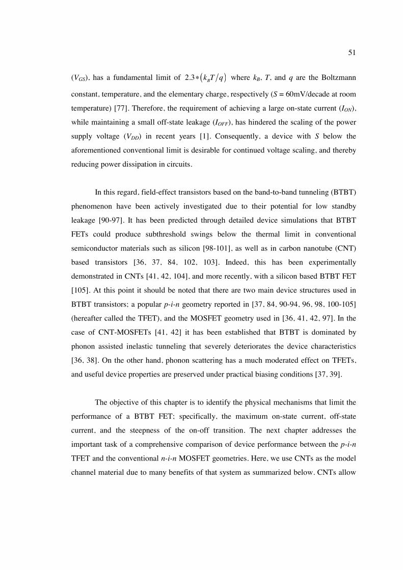
51
(VGS), has a fundamental limit of ( )2.3 Bk T q∗ where kB, T, and q are the Boltzmann
constant, temperature, and the elementary charge, respectively (S = 60mV/decade at room
temperature) [77]. Therefore, the requirement of achieving a large on-state current (ION),
while maintaining a small off-state leakage (IOFF), has hindered the scaling of the power
supply voltage (VDD) in recent years [1]. Consequently, a device with S below the
aforementioned conventional limit is desirable for continued voltage scaling, and thereby
reducing power dissipation in circuits.
In this regard, field-effect transistors based on the band-to-band tunneling (BTBT)
phenomenon have been actively investigated due to their potential for low standby
leakage [90-97]. It has been predicted through detailed device simulations that BTBT
FETs could produce subthreshold swings below the thermal limit in conventional
semiconductor materials such as silicon [98-101], as well as in carbon nanotube (CNT)
based transistors [36, 37, 84, 102, 103]. Indeed, this has been experimentally
demonstrated in CNTs [41, 42, 104], and more recently, with a silicon based BTBT FET
[105]. At this point it should be noted that there are two main device structures used in
BTBT transistors; a popular p-i-n geometry reported in [37, 84, 90-94, 96, 98, 100-105]
(hereafter called the TFET), and the MOSFET geometry used in [36, 41, 42, 97]. In the
case of CNT-MOSFETs [41, 42] it has been established that BTBT is dominated by
phonon assisted inelastic tunneling that severely deteriorates the device characteristics
[36, 38]. On the other hand, phonon scattering has a much moderated effect on TFETs,
and useful device properties are preserved under practical biasing conditions [37, 39].
The objective of this chapter is to identify the physical mechanisms that limit the
performance of a BTBT FET; specifically, the maximum on-state current, off-state
current, and the steepness of the on-off transition. The next chapter addresses the
important task of a comprehensive comparison of device performance between the p-i-n
TFET and the conventional n-i-n MOSFET geometries. Here, we use CNTs as the model
channel material due to many benefits of that system as summarized below. CNTs allow

52
1-dimensional carrier transport without depletion capacitance effects, and high
performance transistors that operate near the ballistic limit have already been
demonstrated [13-15]. They also have a direct energy bandgap and small carrier effective
masses that are conducive to BTBT devices [8]. Furthermore, a detailed simulation
framework has been developed for modeling carrier transport through CNT transistors
[35, 71, 72, 106], and benchmarked against experiments [14, 38, 72]. Therefore, p-i-n
TFET operation can be comprehensively explored using CNTs as the channel material,
realistically treating effects such as phonon scattering. Although we use the CNT as a
model channel material, the general conclusions are expected to be broadly applicable to
this class of devices fabricated in different materials.
5.2 Ballistic Operation of p-i-n TFETs
Section 4.2 described the BTBT operation in CNT-MOSFETs, wherein it was
Figure 5.1. (a) Gated CNT p-i-n Tunnel FET with wrapped around high-k cylindrical gate geometry, (b) Equilibrium band diagram for the p-i-n Tunnel FET.
A (13,0) zigzag CNT with EG 0.8eV is being used.

53
found that phonon-assisted inelastic tunneling dominated the device characteristics. That
led to a severe degradation of the desirable subthreshold properties such as the steep
subthreshold slope. The BTBT device described in section 4.2 suffers from two additional
geometrical properties that limit its performance: 1) presence of two tunneling barriers, 2)
longitudinal quantization of the electronic states in the channel region that reduces the
density of states for carrier conduction. Both these properties detrimentally affect the
device current, thus limiting its performance. These limitations imposed by the CNT-
MOSFET structure can be circumvented by using a p-i-n based device geometry ([37] and
references therein, [84]).
The CNT p-i-n Tunnel FET shown in Figure 5.1 (a) has a wrapped-around high-k
gate oxide and, doped source (p-type) and drain (n-type) regions. The equilibrium band
diagram is shown in Figure 5.1 (b). Ballistic NEGF simulations have been performed as
described in Chapter 2. Figure 5.2 shows some specific results for the p-i-n device under
on-state biasing conditions. Figure 5.2 (a) is the energy-position resolved electron density,
which is essentially the integrand of Eq. (2.15). It clearly shows that electrons in the p-
type source region are filled up to the Fermi level (EF1) which is below the valence band
edge. Similarly, electrons in the n-type drain are filled up to EF2 which is above the
Figure 5.2. (a) Energy-position resolved electron density distribution, (b) Energy-position resolved current density distribution (log scale).

54
conduction band edge. Under the on-state biasing conditions, we apply a positive drain
bias and a positive gate bias which pushes down the bands in the channel region. As seen
in Figure 5.2 (a), a tunneling barrier opens up near the source-channel junction and a net
device current flows. This can be clearly seen in Figure 5.2 (b) which is an energy-
position resolved current density distribution, i.e: the integrand of Eq. (2.18). At this
point, comparing Figure 5.2 (b) and Figure 4.7 (c), the benefits of the p-i-n Tunnel FET
geometry are evident. Unlike in the CNT-MOSFET, the new geometry has only one
tunneling barrier. Furthermore, the electronic states in the channel region are not
quantized in the latter geometry, resulting in an increased density of states. Both these
features are expected to improve the device current compared to BTBT in the CNT-
MOSFET geometry, thus increasing performance. It is important to note that the p-i-n
Tunnel FET geometry can lead to ambipolar transport characteristics. This can be easily
understood by observing Figure 5.2 for the case of a negative gate bias, in the direction of
turning off the device. Under such biasing conditions the bands in the channel will be
pulled up, and a tunneling barrier will appear at the drain-channel junction. Carriers will
tunnel through this junction giving rise to an ambipolar current. In this regard, the CNT p-
i-n Tunnel FET has similar behavior compared to the Schottky-barrier CNTFET
operation [83].

55
The output characteristics (IDS-VDS) under ballistic operation for the p-i-n Tunnel
FET are shown in Figure 5.3. It is seen that the device operates similar to an n-type
enhancement mode transistor, and on-currents of ~ 1 µA/tube are easily achieved. Even
though the device currents attained for the p-i-n Tunnel FETs are larger than the BTBT
currents for CNT-MOSFETs, they are still considerably smaller than that observed for
conventional over-the-barrier operation. Comparing Figure 4.1 and Figure 5.3 it is
evident that the conventional operation gives currents about 20 times larger compared to
the p-i-n operation. Since the device performance critically depends on the current drive,
it is important to compare the characteristics of the two devices in detail, in order to
understand their pros and cons. We address this important task in the next chapter.
5.3 Influence of Phonon Scattering on Above-Threshold Operation
The modeled CNT p-i-n TFET structure with wrap-around gate used for this study
is similar to that in Figure 5.1 (a). A (16,0) zigzag CNT with high-k HfO2 (k = 16, tox =
2nm ) gate oxide, intrinsic channel (Lch = 20nm), doped source (p-type, NS = 0.75/nm, LS
= 35nm) and drain (n-type, ND = 0.75/nm, LD = 35nm) have been used with Lext = 0nm .
Figure 5.3. IDS-VDS results for CNT p-i-n Tunnel FET shown in Figure 5.1. VGS is varied from 0 to 0.6V in steps of 0.1V. A (13,0) zigzag CNT is used.
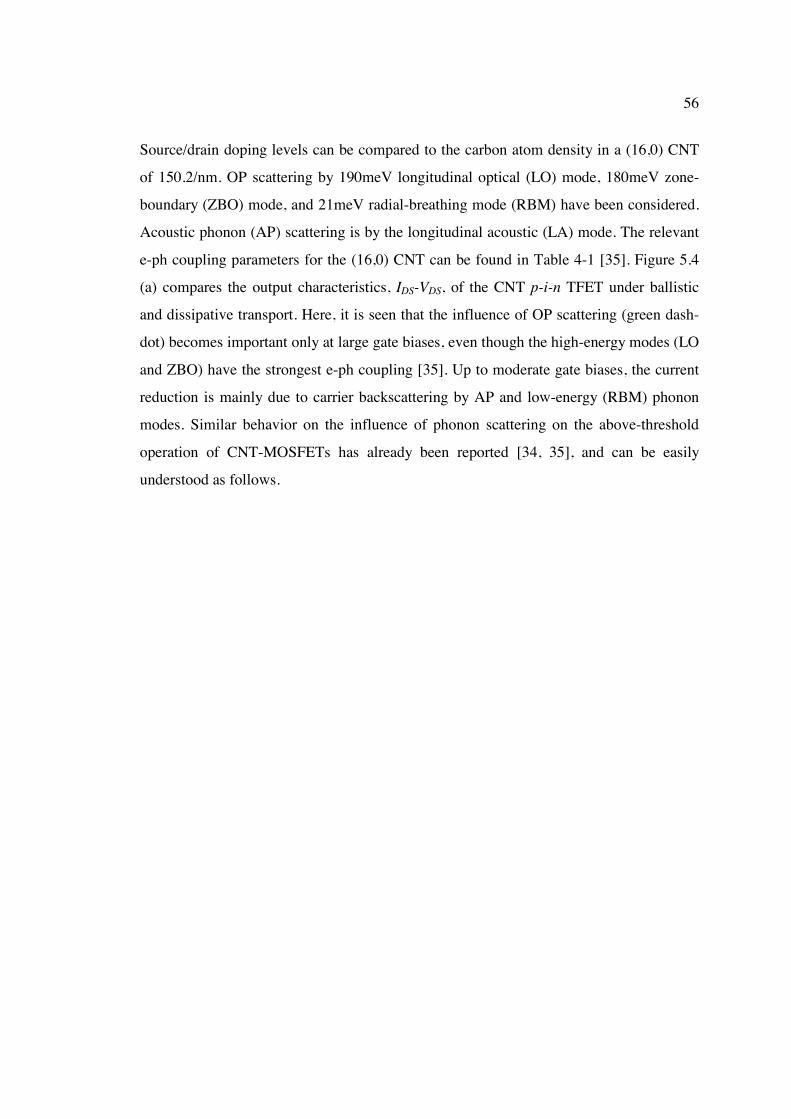
56
Source/drain doping levels can be compared to the carbon atom density in a (16,0) CNT
of 150.2/nm. OP scattering by 190meV longitudinal optical (LO) mode, 180meV zone-
boundary (ZBO) mode, and 21meV radial-breathing mode (RBM) have been considered.
Acoustic phonon (AP) scattering is by the longitudinal acoustic (LA) mode. The relevant
e-ph coupling parameters for the (16,0) CNT can be found in Table 4-1 [35]. Figure 5.4
(a) compares the output characteristics, IDS-VDS, of the CNT p-i-n TFET under ballistic
and dissipative transport. Here, it is seen that the influence of OP scattering (green dash-
dot) becomes important only at large gate biases, even though the high-energy modes (LO
and ZBO) have the strongest e-ph coupling [35]. Up to moderate gate biases, the current
reduction is mainly due to carrier backscattering by AP and low-energy (RBM) phonon
modes. Similar behavior on the influence of phonon scattering on the above-threshold
operation of CNT-MOSFETs has already been reported [34, 35], and can be easily
understood as follows.
57
In order to have current reduction due to scattering by high-energy phonons, a
majority of forward going carriers (source drain) should be backscattered into empty
backward going states by OP emission. Thus, the energy requirements for effective
backscattering depends on the condition, ( )FS C channel FSE E η ω−− = ≥ , where FSE and
C channelE − are the source Fermi level, and the channel conduction band position,
Figure 5.4. (a) Above-threshold IDS-VDS characteristics for the CNT p-i-n TFET. All the optical phonon modes (LO, ZBO, and RBM) are considered simultaneously for OP
scattering. LA mode is considered for AP scattering. (b) Energy-position resolved current density spectrum (i.e., integrand of Eq. (2.18)) at VDS = VGS = 0.5V confirms the reduced
influence of high-energy OP scattering on DC current transport up to moderate gate biases.

58
respectively (see Figure 5.4 (b)) [34]. This is further exemplified in the energy-position
resolved current density spectrum shown in Figure 5.4 (b). After reaching the drain
region, however, carriers can be efficiently scattered by OP emission down to empty low-
lying states, and thus will not possess enough energy to surmount the channel barrier and
reach the source region again. On the other hand, elastic scattering due to acoustic and
low-energy phonons can effectively backscatter at all gate biases, and is the dominant
mechanism until high-energy OP scattering becomes effective at larger gate biases.
Therefore, in Figure 5.4 (a) above-threshold performance is only moderately affected by
phonon scattering. We observe, however, a lower value of the on-current (by about
4~10x) in the CNT p-i-n TFET compared to that of conventional CNT-MOSFETs [34,
35] due to the presence of the tunneling barrier. This observation confirms that the on-
state performance of p-i-n TFETs is mainly dominated by the tunneling barrier properties,
and moderately affected by the channel itself [98, 100, 103].
5.4 Influence of Phonon Scattering on Subthreshold Operation
The subthreshold (off-state) operation is discussed next. Figure 5.5 (a) shows the
transfer characteristics, IDS-VGS, for the CNT p-i-n TFET. Note that only the 180meV
ZBO phonon mode, with strongest e-ph coupling, is included here since the subthreshold
properties are observed to be mainly determined by this mode. In Figure 5.5 (a) it is seen
that the p-i-n TFET has ambipolar behavior, which can be easily understood by observing
Figure 5.4 (b). For small gate biases (or negative biases), the bands in the channel are
pulled up, and a tunneling path appears at the channel-drain junction leading to ambipolar
transport. As expected, the ambipolar branch appears earlier for larger drain biases. For
identical source/drain doping concentrations the IDS-VGS curves are symmetric around the
minimum point. Asymmetric doping schemes can, however, suppress the ambipolar
branch up to larger gate biases and lead to more desirable device characteristics [37]. It
should be noted that, unlike in a conventional MOSFET, the subthreshold swing (S) of a
p-i-n TFET is not a constant, but is bias dependent as seen in Figure 5.5 (a) [98, 99, 103].
Interestingly, we observe less than 60mV/dec S at room temperature for both ballistic and

59
dissipative transport (blue solid and red dashed curves); in our model device, S <
60mV/dec is obtained for VGS < 0.32V (left of dashed vertical line).
In Figure 5.5 (a) it is evident that the presence of OPs has a significant detrimental
effect on the subthreshold properties; a minimum S of 20mV/dec for ballistic transport (at
VDS = 0.1V) degrades to 35mV/dec in the presence of OPs at room temperature (T =
300K). The degradation is even greater at higher device temperatures; minimum S
40mV/dec at T = 400K (VDS = 0.1V). The main reason for such deterioration of S is due
Figure 5.5. (a) IDS-VGS characteristics for the CNT p-i-n TFET at VDS = 0.1V and 0.4V with and without phonon scattering. Simulated device temperatures are as shown in the legend. (b) Energy-position resolved current density spectrum at a device temperature of
400K (VGS = 0.125V, VDS = 0.1V). Phonon absorption assisted transport is clearly observed at the source-channel junction. Carriers thermalize after reaching the drain.

60
to phonon absorption assisted transport as exemplified in Figure 5.5 (b). Under the
ballistic approximation, the minimum off-state current is mainly due to direct source to
drain tunneling through the channel barrier region, and can be made very small; longer
channel lengths, Lch, further suppresses the off-current, and S < 10mV/dec can be
achieved for ballistic transport. Under such biasing conditions, however, higher-order
processes such as phonon absorption assisted transport become significant, and tend to
dominate the off-state characteristics. From Eqs. (3.7) and (3.8) it is seen that the phonon
absorption assisted process is proportional to the phonon occupation number, nω , and
increases at higher device temperatures (Eq. (3.3)). Thus, even though the direct tunneling
processes are expected to be fairly temperature independent [98, 99, 103], higher-order
processes such as phonon assisted transport that are temperature dependent can become
important in the off-state of a BTBT device as seen here. They could also limit the
desirable off-state characteristics that could have been achieved otherwise. At the same
time, the on-state performance of the CNT p-i-n TFET is observed to be relatively
temperature insensitive, and can be attributed to the fact that the above-threshold
transport is mainly due to direct tunneling. In indirect bandgap semiconductors, such as
technologically important silicon and germanium, BTBT would be mainly due to phonon
assisted transport [107, 108], and could have strong temperature dependence both in the
off-state as well as the on-state.
In summary, we observe less than 60mV/dec subthreshold swings in p-i-n TFETs,
in contrast to that in conventional (e.g. n-i-n) MOSFETs operating in the over-the-barrier
conduction regime. The on-current of p-i-n TFETs is, however, mainly dependent on the
tunneling barrier properties, and phonon scattering has only a moderate effect. On the
other hand, the subthreshold operation is dominated by phonon assisted transport, and
exhibits significant temperature dependence. Nevertheless, the low subthreshold swing is
robust and persists even with the inclusion of phonon scattering and under higher source-
to-drain biases.
61
6. PERFORMANCE COMPARISON BETWEEN CNT BASED P-I-N TUNNEL FET AND CONVENTIONAL MOSFET GEOMETRIES
A detailed description of the operation of CNT based p-i-n Tunnel FETs (TFETs)
was presented in the previous chapter. The influence of phonon scattering on the
subthreshold operation as well as the on-state performance was discussed. It was seen that
phonon assisted tunneling tends to degrade the desirable subthreshold characteristics of
TFETs. It also resulted in increasing the off-state leakage current at higher temperatures.
Under on-state operation, phonon scattering had a relatively small effect on device
current. The presense of the tunneling barrier itself was more detrimental towards the
current drive capability. Therefore, it is important comprehensvliy compare the p-i-n
device performance to the conventional MOSFET operation under realistic transport
conditions. This will allow us to understand the true potentials of the p-i-n geometry over
the conventional MOSFET, and any shortcomings that need to be addressed before it can
become a useful device technology.
In this chapter we address this important task of a comprehensive comparison
between the two geometries. We use CNTs as the model channel material due to many
benefits of that system as described in section 5.1. Previous work has also compared CNT
transistor performance to that of silicon transistors [109-111] and to that based on silicon
nanowires [112]. Here we use similar device metrics to compare the performance
between TFETs and MOSFETs using a uniform simulation environment for both the
devices. Note that this chapter is adapted from [40]
The model device structure used in this study, shown in Figure 6.1, has a
cylindrical wrap-around gate and doped source/drain regions. In this study we have
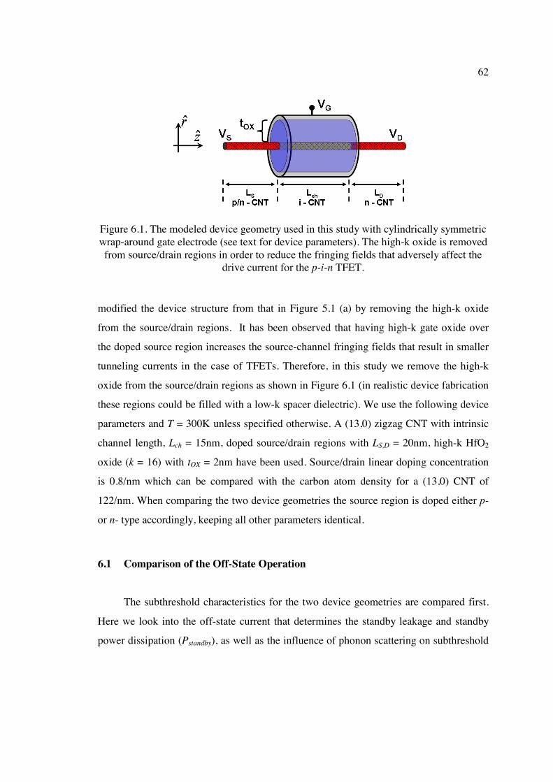
62
modified the device structure from that in Figure 5.1 (a) by removing the high-k oxide
from the source/drain regions. It has been observed that having high-k gate oxide over
the doped source region increases the source-channel fringing fields that result in smaller
tunneling currents in the case of TFETs. Therefore, in this study we remove the high-k
oxide from the source/drain regions as shown in Figure 6.1 (in realistic device fabrication
these regions could be filled with a low-k spacer dielectric). We use the following device
parameters and T = 300K unless specified otherwise. A (13,0) zigzag CNT with intrinsic
channel length, Lch = 15nm, doped source/drain regions with LS,D = 20nm, high-k HfO2
oxide (k = 16) with tOX = 2nm have been used. Source/drain linear doping concentration
is 0.8/nm which can be compared with the carbon atom density for a (13,0) CNT of
122/nm. When comparing the two device geometries the source region is doped either p-
or n- type accordingly, keeping all other parameters identical.
6.1 Comparison of the Off-State Operation
The subthreshold characteristics for the two device geometries are compared first.
Here we look into the off-state current that determines the standby leakage and standby
power dissipation (Pstandby), as well as the influence of phonon scattering on subthreshold
Figure 6.1. The modeled device geometry used in this study with cylindrically symmetric wrap-around gate electrode (see text for device parameters). The high-k oxide is removed from source/drain regions in order to reduce the fringing fields that adversely affect the
drive current for the p-i-n TFET.

63
operation for the two devices. Drain induced degradation of subthreshold characteristics,
which is important for highly scaled devices, is also discussed.
6.1.1 Subthreshold slope, off-current (IOFF), and standby power dissipation
(Pstandby)
One of the main attractions for BTBT transistors has been their potential to reduce
Figure 6.2. IDS-VGS dependence on temperature for, (a) n-i-n MOSFET and, (b) p-i-n TFET under ballistic and dissipative transport. The latter has reduced temperature
dependence under ballistic conditions. Phonon assisted tunneling can, however, degrade the subthreshold characteristics.

64
off-state leakage, and in turn, standby power dissipation (Pstandby) in circuits. This is
achieved through subthreshold operation with S below the conventional limit in these
devices. Figure 6.2 compares the temperature dependence of the transfer characteristics
(IDS-VGS) for the two geometries. The ballistic results (solid curves) are discussed first. In
Figure 6.2 (a) it is observed that we obtain ideal subthreshold operation with S =
60mV/dec (at T = 300K) due to the superior electrostatic control by the wrap-around gate.
At higher temperatures, however, S degrades proportionately. This can be easily
understood by observing Figure 6.3 (a) showing the thermionic emission mechanism in
the off-state of a conventional MOSFET. The high energy tail of the Fermi distribution
grows with temperature as ( )exp BE k T− leading to the aforementioned degradation of
S. Furthermore, in integrated circuits this results in higher off-state leakage currents and
Pstandby. This could lead to a positive feedback mechanism between the two, known as
thermal runaway, that could ultimately destroy the circuit [113].
On the other hand, the ballistic results for the TFET (Figure 6.2 (b)) clearly shows
S < 60mV/dec operation at room temperature. This is easily understood by examining
Figure 6.3 (b) where the high energy tail of the Fermi distribution for electrons lies inside
the p-type source bandgap region. Therefore, when the conduction band in the channel is
pulled above the valence band of the source, an abrupt reduction in device current is
Figure 6.3. Band diagram and the source Fermi distribution for, (a) n-i-n MOSFET and, (b) p-i-n TFET. In the latter, high-energy part of the source distribution is cutoff by the
bandgap region leading to < 60mV/decade subthreshold swing. Phonon assisted tunneling becomes important under these conditions.

65
expected, which leads to S values much smaller than the conventional limit [103]. In
Figure 6.2 (b) an interesting observation is that the off-state current under ballistic
transport does not significantly degrade at elevated temperatures. This is due to the
elimination of high energy thermal injection within the source bandgap region. There is a
slight increase in subthreshold current at higher temperatures related to the broadening of
Figure 6.4. IOFF vs. ION dependence on temperature at VDD = 0.3V under, (a) ballistic and, (b) dissipative transport. Shaded region is where the p-i-n TFET has an advantage over
the n-i-n MOSFET due to larger ION with a smaller IOFF. Temperature dependence of IOFF for the p-i-n TFET is also smaller than that for the latter.

66
the Fermi distribution near EFS (see Figure 6.3 (b)). The possibility of achieving off-stage
leakage currents that do not degrade at higher temperatures is an attractive feature of
TFETs that could potentially alleviate the thermal runaway problem mentioned earlier.
The relative benefits of the TFET over the MOSFET geometry in the off-state can
be better compared through the IOFF vs. ION (at a constant VDD) results shown in Figure
6.4 (a) for ballistic operation. Here, the IOFF-ION curves are generated by scanning the IDS-
VGS results in Figure 6.2 with a constant VDD bias window as explained in Ref. [109]. In
Figure 6.4 (a) the increase in IOFF at smaller ION values (ION 0.6µA/tube) observed for
the TFET is due to ambipolar conduction seen in Figure 6.2 (b). Figure 6.4 (a) clearly
shows the suppression of IOFF degradation at higher temperatures under ballistic transport
in the case of TFETs compared to MOSFETs. Furthermore, the shaded region of Figure
6.4 (a) corresponds to the range of device biasing conditions where the TFET has the
benefit over the MOSFET. Within this region it is observed that the former has a smaller
IOFF (thus smaller Pstandby) at a given ION (looking vertically). Conversely, the TFET can
deliver a larger ION at a given IOFF (looking horizontally). It is noted that in this region the
TFET can only deliver a few µA of drive current per CNT. Therefore, these devices
might be better suited for low power applications with moderate drive current
requirements.
6.1.2 Comparative influence of phonon scattering
The influence of phonon scattering on the transfer characteristics is shown by the
dashed curves of Figure 6.2 (see Refs. [34, 36, 38, 39] for detailed information on each
geometry). In Figure 6.2 (a) it is observed that phonon scattering has only a small effect
on the subthreshold properties of the MOSFET which are dominated by the thermionic
emission component of current conduction. Nevertheless, at small gate biases the onset of
ambipolar conduction is seen due to phonon assisted inelastic tunneling that turns on
BTBT in CNT-MOSFETs at an earlier voltage [36, 38]. In the case of the TFET in Figure

67
6.2 (b) it is observed that S degrades in the presence of phonon scattering even though S <
60mV/dec is still attained. This deterioration is due to phonon absorption assisted
transport playing an important role under off-state biasing conditions (see Figure 6.3 (b)
and Figure 5.5 (b)) [39]. More importantly, the subthreshold current becomes temperature
dependent due to larger phonon occupation (eq. (3.3)) at higher temperatures that
increases phonon absorption assisted transport (second term of eqs. (3.7) and (3.8)).
Nevertheless, examining Figure 6.4 (b) we observe that there still exists a possible
biasing region (shaded) where the TFET outperforms the MOSFET geometry. The
significant increase in IOFF at higher temperatures is clearly observed for the TFET. Off-
state leakage that is about an order of magnitude smaller compared to the MOSFET can
still be attained at both room and elevated temperatures. In comparing Figure 6.4 (a) and
(b), however, it is clear that the ballistic operation of TFETs could have reduced the off-
state leakage significantly, especially at higher temperatures. Therefore, it can be
summarized that the TFET can indeed deliver superior subthreshold characteristics under
realistic transport conditions, but phonon scattering deteriorates the beneficial features
that could have been attained otherwise.
6.1.3 Drain induced off-state degradation
In this section we examine the effect of the drain bias on subthreshold properties. In a
conventional MOSFET this could lead to the well known drain induced barrier lowering
(DIBL) effect [77]. In the case of a TFET in the off-state, as shown in Figure 6.3 (b), it is
not clear whether DIBL could necessarily have a similar effect since the high energy tail
of the Fermi distribution is already within the source bandgap region. Therefore, in order
to study the effect of the drain bias on subthreshold current we use a slightly modified
device geometry compared to Figure 6.1 that allows drain field penetration into the
channel region in our wrap-around gate structure. In this section we use a (10,0) CNT
with tOX = 5nm and SiO2 (k = 3.9) for the gate oxide that covers the full length of the tube
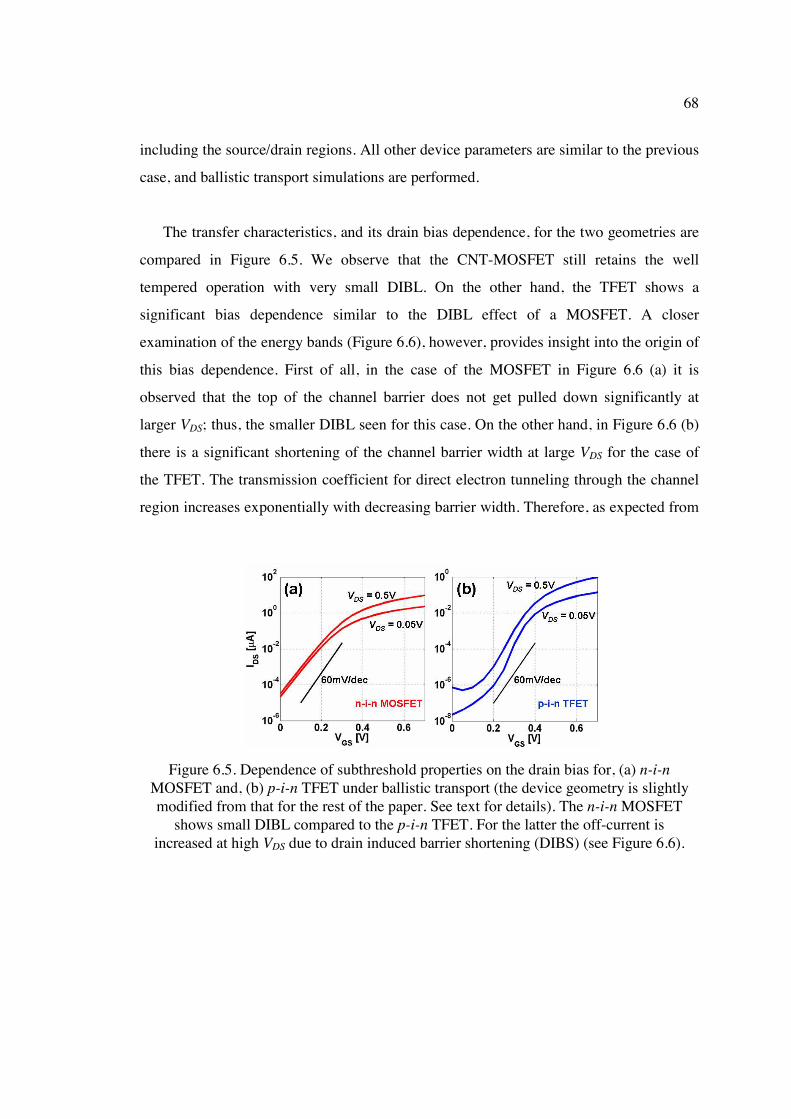
68
including the source/drain regions. All other device parameters are similar to the previous
case, and ballistic transport simulations are performed.
The transfer characteristics, and its drain bias dependence, for the two geometries are
compared in Figure 6.5. We observe that the CNT-MOSFET still retains the well
tempered operation with very small DIBL. On the other hand, the TFET shows a
significant bias dependence similar to the DIBL effect of a MOSFET. A closer
examination of the energy bands (Figure 6.6), however, provides insight into the origin of
this bias dependence. First of all, in the case of the MOSFET in Figure 6.6 (a) it is
observed that the top of the channel barrier does not get pulled down significantly at
larger VDS; thus, the smaller DIBL seen for this case. On the other hand, in Figure 6.6 (b)
there is a significant shortening of the channel barrier width at large VDS for the case of
the TFET. The transmission coefficient for direct electron tunneling through the channel
region increases exponentially with decreasing barrier width. Therefore, as expected from
Figure 6.5. Dependence of subthreshold properties on the drain bias for, (a) n-i-n MOSFET and, (b) p-i-n TFET under ballistic transport (the device geometry is slightly modified from that for the rest of the paper. See text for details). The n-i-n MOSFET
shows small DIBL compared to the p-i-n TFET. For the latter the off-current is increased at high VDS due to drain induced barrier shortening (DIBS) (see Figure 6.6).

69
eq. (2.19) the off-state current increases significantly. This effect for TFETs observed
here can be identified as drain induced barrier shortening (DIBS). It should be noted that
DIBS would be important for a highly scaled device where short channel effects are
considerable. If the original channel barrier width (~ Lch) were long enough, the actual
magnitude of direct tunneling current would be very small even in the presence of barrier
shortening effects.
6.2 Comparison of the On-State Performance
The on-state device performance of the two geometries is compared next. In this
regard we use a few popular device metrics such as the on-current (ION), intrinsic device
Figure 6.6. Band diagram in the off-state for, (a) n-i-n MOSFET and, (b) p-i-n TFET at different drain biases. For the latter, drain induced barrier shortening (DIBS) is observed
which increases the tunneling current through the channel barrier exponentially.

70
delay metric (), and power-delay product (PDP) which is essentially the switching energy
of the transistor [77]; The latter two metrics, and PDP, relate to the intrinsic operation
of the transistor where it switches from the on-state to the off-state, or vice versa.
6.2.1 On-current (ION)
One of the main concerns for BTBT based transistors has been their ability to
deliver considerable drive currents. The use of TFETs with only one tunneling barrier for
carriers as opposed to BTBT in MOSFETs [36, 41, 42, 97] where there are two, the on-
current for the former has improved. And, even though there have been many
optimization strategies proposed for TFETs in order to improve ION further [37, 98, 101-
103] it still remains a challenge. Figure 6.7 compares IDS-VGS in linear scale for the two
devices shown in Figure 6.1. It is observed that the drive current for the TFET is about 3x
smaller than that for the MOSFET. If the high-k oxide covers the CNT throughout,
including the source region, ION further degrades by about 18x compared to the MOSFET
Figure 6.7. Linear IDS-VGS comparison for the n-i-n MOSFET and p-i-n TFET under ballistic and dissipative transport. The on-current for the latter is reduced due to the
presence of the tunneling barrier.

71
(not shown). In Figure 6.7, however, it is observed that phonon scattering has only a
minor effect on TFET on-state current (reduces by ~ 10%) compared to the MOSFET
(reduces by ~ 16%). This is because in the case of the former the back-scattered carriers
in the channel region have a larger probability of being reflected back by the source-
channel tunneling barrier, ultimately escaping into the drain. Thus, DC current transport
is not significantly affected by phonon scattering. Therefore, from Figure 6.7 it can be
noted that the tunneling barrier properties of a TFET have a much dominant effect on the
drive current, and the channel mobility itself has only a comparatively minor influence
[39, 98, 100, 103].
6.2.2 Intrinsic device delay metric ()
Intrinsic device delay () is an important performance metric that corresponds to
intrinsic limitations on switching speed and AC operation of a transistor [77]. In this
Figure 6.8. Intrinsic device delay metric () vs. ION/IOFF comparison. Surprisingly, p-i-n TFET shows similar delay compared to the n-i-n MOSFET even though the former has a
smaller drive current (Figure 6.7). Also, p-i-n TFET even becomes faster at larger ION/IOFF operating regime. In the presence of a load capacitance, however, the actual drive current will become important and the p-i-n TFET could be relatively slower.

72
work the switching speed is calculated by, ( )ON OFF ONQ Q Iτ = − , instead of the
traditional equation of g DD ONC V Iτ = [77] due to the strong bias dependence of gate
capacitance, Cg (see Section 6.3). Here, ,ON OFFQ is the total charge induced in the
transistor in the on- and off-states, respectively (calculated similar to ION,OFF with a
constant VDD bias window [109]). Thus, accounts for any additional charging induced
by fringe capacitance effects. Figure 6.8 shows the vs. ION/IOFF comparison for the
TFET and the MOSFET. Surprisingly, we observe that for the former is comparable to
that of the latter even though the MOSFET has a much larger drive current (Figure 6.7).
At larger ION/IOFF ratios (> 104) the TFET is even faster. The main reason for this
behavior is the amount of charge involved in the on-off transition of a TFET is
considerably smaller compared to that for the MOSFET (see Section 6.3). Device delay,
however, increases significantly (not shown) when high-k oxide covers the full length of
the CNT including the source region due to the reduction in ION.
In Figure 6.8 it is also observed that phonon scattering increases for both the
devices. Even though the drive current for the TFET does not considerably deteriorate in
the presence of phonon scattering (Figure 6.7) the degradation of is comparatively
larger. This is due to the occupation of negative going states (-k) in the channel in the
presence of back-scattering, and the occupation of low energy states with smaller band
velocities, which increase the average transit time for carriers. A similar effect has also
been reported in Schottky barrier CNTFETs [114]. Finally, it should be noted that even
though the intrinsic delay in Figure 6.8 is comparable for the two geometries, the TFET
could become significantly slower in the presence of a load capacitance (such as a long
interconnect). In such cases the actual drive current of the device becomes important and
the MOSFET would have a considerable advantage (Figure 6.7).

73
6.2.3 Power-delay product (PDP) and Dynamic power dissipation (Pdynamic)
Power-delay product (PDP) is the switching energy required for on-off transition
of a transistor. It is a measure of the dynamic power dissipation, ( )dynamicP PDP fα= ,
where f is the operating frequency and the activity factor [77]. In this work we calculate
PDP by, ( )ON OFF DDPDP Q Q V= − , that corresponds to charging of the MOS capacitor
under the voltage bias VDD. Figure 6.9 compares the PDP vs. ION/IOFF for the two
geometries. Here, it is observed that the TFET has a smaller switching energy compared
to the MOSFET. Furthermore, the relative shapes of the two curves appear to be
fundamentally different; the MOSFET curve is concave down while that for the TFET is
concave up, thus resulting in a smaller PDP under practical biasing conditions (similar
distinctions for the two geometries have been consistently observed under various device
parameters [37]).
Figure 6.9. Comparison of the power-delay product (PDP = switching energy). p-i-n TFET has a significant benefit here, and shows a fundamentally different behavior
compared to the n-i-n MOSFET.
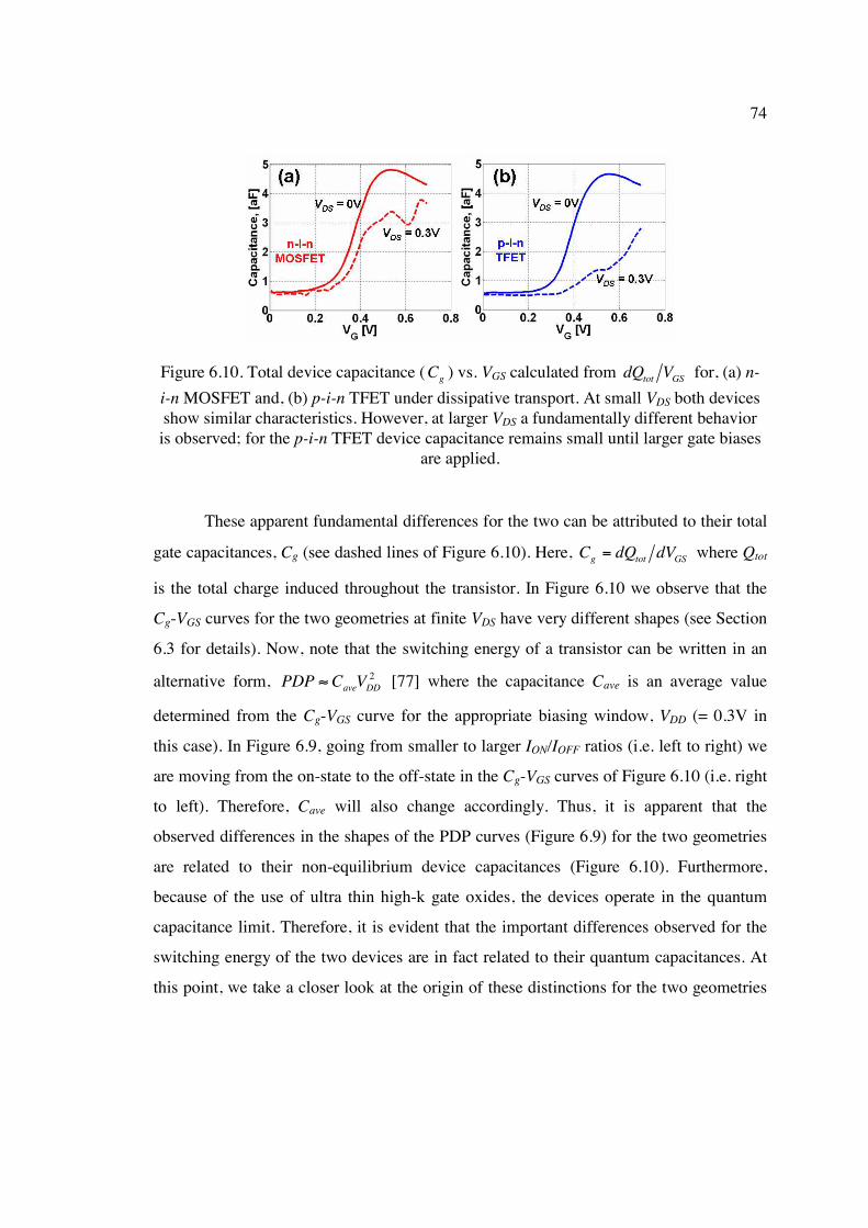
74
These apparent fundamental differences for the two can be attributed to their total
gate capacitances, Cg (see dashed lines of Figure 6.10). Here, g tot GSC dQ dV= where Qtot
is the total charge induced throughout the transistor. In Figure 6.10 we observe that the
Cg-VGS curves for the two geometries at finite VDS have very different shapes (see Section
6.3 for details). Now, note that the switching energy of a transistor can be written in an
alternative form, 2ave DDPDP C V≈ [77] where the capacitance Cave is an average value
determined from the Cg-VGS curve for the appropriate biasing window, VDD (= 0.3V in
this case). In Figure 6.9, going from smaller to larger ION/IOFF ratios (i.e. left to right) we
are moving from the on-state to the off-state in the Cg-VGS curves of Figure 6.10 (i.e. right
to left). Therefore, Cave will also change accordingly. Thus, it is apparent that the
observed differences in the shapes of the PDP curves (Figure 6.9) for the two geometries
are related to their non-equilibrium device capacitances (Figure 6.10). Furthermore,
because of the use of ultra thin high-k gate oxides, the devices operate in the quantum
capacitance limit. Therefore, it is evident that the important differences observed for the
switching energy of the two devices are in fact related to their quantum capacitances. At
this point, we take a closer look at the origin of these distinctions for the two geometries
Figure 6.10. Total device capacitance ( gC ) vs. VGS calculated from tot GSdQ V for, (a) n-i-n MOSFET and, (b) p-i-n TFET under dissipative transport. At small VDS both devices show similar characteristics. However, at larger VDS a fundamentally different behavior is observed; for the p-i-n TFET device capacitance remains small until larger gate biases
are applied.

75
since that provides useful insights into the fundamental differences in the relevant device
physics.
6.3 Device Operation at the Quantum Capacitance Limit
The continual rise in gate oxide capacitances, along with the importance of carrier
transport in confined structures, have made the quantum capacitance limit of device
operation increasingly relevant; i.e. OX QC C condition where OXC and QC are the gate
oxide and quantum capacitance, respectively [115, 116]. And, QC is related to the
average density of states (DOS) near the Fermi level, ( )Q FC DOS E [21]. As discussed
below, in TFET structures the DOS can become very small, thus the aforementioned
condition can be easily achieved. In this case the gate capacitance is dominated by QC
itself; ( ) ( )g OX Q OX Q QC C C C C C= + ≈ .
Figure 6.10 compares the bias dependence of Cg for the two devices under
dissipative transport (similar behavior is obtained under ballistic transport as well). It is
Figure 6.11. Energy-position resolved electron distribution for, (a) n-i-n MOSFET and, (b) p-i-n TFET under ballistic transport at VGS = 0.5V, VDS = 0.3V. A significantly
higher occupation of channel states is observed for the former.

76
observed that the equilibrium Cg-VGS curves (solid) for the two are very similar, and carry
the characteristic signature of the CNT-DOS [8]. This relationship has also been
experimentally verified in the case of CNT-MOSFETs [117]. At larger VDS, however,
interesting differences arise. First of all, in the case of the MOSFET the initial peak splits
into two. This is because the negative going (-k) half of channel DOS is filled only at a
larger VGS compared to the positive going (+k) ones [116]. On the other hand, Cg-VGS
curve for the TFET remains notably small up to larger gate biases. This means that the
charge induced in the channel for the TFET is considerably lower compared to that for
the MOSFET. This difference can be clearly observed in the energy-position resolved
electron distribution function (eq. (2.11)) shown in Figure 6.11. There, the +k states in the
channel of the MOSFET that are below the source Fermi energy (EFS) are well occupied.
On the other hand, in the case of the TFET even though the conduction band in the
channel is well below the source EFS the channel states are relatively empty. This is due to
the presence of the tunneling barrier that hinders carrier injection into the channel from
the source reservoir [103, 116].
Since QC in fact originates from the filling of the channel DOS by the source and
Figure 6.12. Reservoir resolved LDOS for the n-i-n MOSFET at VGS = 0.5V, VDS = 0.3V: (a) source-evolving states (LODSS), (b) drain-evolving states (LDOSD). There is a
significant amount of source-evolving states inside the channel that are filled by the source Fermi distribution. Drain-evolving states in the channel are not filled at larger VDS.

77
drain reservoirs, it is instructive to distinguish the origin of these states by the two
contacts of the transistor. This is achieved by looking at the contact resolved LDOS (from
eq. (2.14)) shown in Figure 6.12 and Figure 6.13 for the MOSFET and the TFET,
respectively. This separation is strictly possible under ballistic transport, but it elucidates
the underlying physical reasons for the differences seen for the two device geometries. In
Figure 6.12 it is observed that there is a significant amount of source-evolving (+k) states
inside the channel that is filled by that reservoir. This leads to the considerable device
capacitance observed for the MOSFET in Figure 6.10 (a) (dashed curve) when quantum
capacitance has a significant contribution to Cg. At larger gate biases the drain-evolving (-
k) states also get filled by the drain reservoir, further increasing Cg. This behavior leads to
the splitting of the single peak in Cg-VGS curve under equilibrium conditions, into two
peaks under larger drain biases.
In Figure 6.13 (a), for the case of the TFET, it is observed that there is only a
small amount of source-evolving states inside the channel which are filled by that
reservoir. Therefore, they have only a small contribution to QC . On the other hand, there
Figure 6.13. Reservoir resolved LDOS for the p-i-n MOSFET at VGS = 0.5V, VDS = 0.3V: (a) source-evolving states (LODSS), (b) drain-evolving states (LDOSD). There is a small amount of source-evolving states inside the channel due to the presence of the tunneling
barrier. These are the states filled by the source Fermi distribution. Interestingly, there is a significant amount of drain-evolving states inside the channel but they are not filled at
large VDS.

78
is a large number of drain-evolving states inside the channel; both –k states, as well as +k
states that originate from the reflection of the former against the tunneling barrier (Figure
6.13 (b)). These states are, however, not occupied by the drain Fermi reservoir at large
VDS. They get filled only at larger gate biases, and will subsequently increase QC as
observed by the dashed curve of Figure 6.10 (b). On the other hand, at small drain biases
these states are easily filled, and dominate QC (solid curve of Figure 6.10 (b)). At this
point, it can be noted that the TFET would have very small QC under non-equilibrium
conditions, and would easily get into the quantum capacitance limit of operation [103].
Furthermore, the characteristic differences in drain bias dependence of QC for the
MOSFET and the TFET should be readily distinguishable from an experiment similar to
[117].
In summary, this chapter presented a comprehensive comparison of device
performance between the conventional MOSFET and the p-i-n TFET geometries. It was
confirmed that the TFET can indeed operate with a subthreshold swing below the
60mV/decade conventional limit, thereby reducing off-state leakage and standby power
dissipation. Phonon assisted tunneling tends to deteriorate the desirable subthreshold
characteristics of a TFET that could have been achieved under ballistic conditions. Under
on-state operation, the drive current and the switching speed of a TFET are dominated by
the tunneling barrier properties, and phonon scattering comparatively has only a minor
effect. On the other hand, at the quantum capacitance limit of device operation, the
switching energy of a TFET is observed to be fundamentally smaller compared to that of
a MOSFET. Therefore, the p-i-n TFET geometry is expected to be a strong candidate for
future low power applications.

79
7. TREATMENT OF INELASTIC TRANSPORT IN CNT OPTOELECTRONIC DEVICES
Electroluminescence and the investigation of potential optoelectronic applications
for CNTs have been a relatively recent research endeavor. This chapter describes the
modeling and simulation of a recently demonstrated optoelectronic device based on a
partially suspended CNTFET [10]. The optical emission in this device has been attributed
to an excitonic process, and the experimentally observed high emission efficiencies have
generated much interest in this class of devices. In section 7.1 we review optical emission
in CNT based devices highlighting the importance of excitonic effects. Section 7.2
describes the simulation method we use in this study. Since the experimentally
investigated devices tend to be at the long channel limit (hundreds of nanometers) we use
a numerical solution of the Botzmann transport equation (BTE) instead of the NEGF
formalism used up to now for quantum transport calculations. Chapter 8 presents a
detailed simulation study, using the methods presented here, for experimentally
demonstrated device geometries. Note that certain parts of this chapter are adapted form
our publications [43, 44].
7.1 Background on Excitonic Emission in CNTs
In recent years, rapid progress in research on carbon nanotube (CNT) electronic
and optoelectronic devices has occurred [5, 118]. High performance CNT transistors
operating close to the ballistic limit have been experimentally realized [13, 15, 16]. The
demonstration of electroluminescence in CNTs has opened up new possibilities for
optoelectronic applications as well [9, 10, 46, 119]. The importance of nanoscale physical
phenomena in governing the operation of CNT devices has been underscored in a

80
multitude of experiments [5, 118]. The first optical emission in a CNTFET was
demonstrated in 2003 by the Avouris’ group at IBM [9]. Since then, a number of
experiments have been reported investigating the optical emission phenomena in these
devices [10, 46, 119].
All these devices had tube lengths of a few micrometers or more, and operated in
the diffusive limit. Optical emission in earlier CNT devices [9, 46] was attributed to free
carrier recombination under ambipolar transport, which is similar to the operation of
conventional light emitting diodes (LEDs). In this case, a Schottky-barrier CNT field-
effect transistor (CNTFET) is operated at high source-drain bias (VDS) such that both
electrons and holes are injected into the channel simultaneously from the two contacts,
respectively [9, 46]. These free carriers radiatively recombine inside the channel region
resulting in optical emission. Device operation was well modeled by drift-diffusion
treatment of carrier transport and free carrier recombination [120-123]. A recent
experiment [10], however, using a partially suspended CNTFET as shown in Figure 7.1
(a) demonstrated an enhancement of optical emission intensities of 100-1000x than that
in the earlier work. The emission process was attributed to exciton generation under
unipolar transport conditions [10].
Figure 7.1 (a) shows a schematic of this novel device. It uses a semiconducting
CNT suspended over a trench that has been created on the oxidized silicon wafer by
reactive ion etching. Pd metal is used for source/drain contacts, and the heavily doped
substrate is used as the back-gate. Interestingly, the optical emission is spatially localized
near the trench-substrate junction near the drain (Figure 7.1 (b)), and it is attributed to
radiative recombination of impact excited excitons in this region [10]. It has already been
well established that the optical processes in CNTs are dominated by excitonic effects
[124, 125]. In the case of the partially suspended CNTFET reported in Ref. [10], as
shown in Figure 7.1 (c), there exists a high electric-field region at the trench-substrate
junction near the drain contact (shown for positive gate bias, VGS > 0). This arises due to

81
the difference in electrostatic coupling to the back-gate in the trench and the substrate
regions, respectively. Electrons injected from the source can gain enough kinetic energy
in this high-field region to generate excitons by impact excitation. The subsequent
radiative recombination of these excitons is expected to lead to localized optical emission
at the trench-substrate junction seen in Ref. [10]. At this point it is important to
differentiate the above mechanism from thermal light emission reported in suspended
metallic CNTs [11, 126, 127]. In the latter case the optical emission is seen in the middle
of the trench region where the local temperature is the highest [11, 128].
Note that excitonic effects in CNTs are expected to be much stronger compared to
conventional semiconductors due to the enhancement of Coulomb interaction in 1D. In
fact, there has been a multitude of both experimental and theoretical work clearly
demonstrating that the photoluminescence (where the initial excitation is due to the
Figure 7.1. (a) A schematic of the CNTFET suspended over a trench with the back-gated geometry, (b) Experimental observation of optical emission localized at the trench-drain junction (from [10]). (c) Band diagram near the trench-substrate junction at the drain end (shown for VGS > 0). Electrons that are injected from the source can gain enough kinetic
energy at this junction for the impact excitation of excitons.

82
absorption of photons) in CNTs is excitonic based [119, 124, 129-149]. The reported
excitonic binding energies (Eb) for CNTs are in the range of 100meV ~ 1eV [139, 143].
Such large binding energies for CNTs should be contrasted with that for conventional
semiconductors, such as GaAs, that is only a several meV’s [150]. Therefore, observation
of excitonic effects in conventional semiconductors requires ultracold experimental
setups. Another important factor that influences the observation of excitonic effects,
especially in devices, is the exciton ionization field (EI). This is the field at which the
bound excitons dissociate due to the opposite forces imposed on the electron and the hole,
and the excitonic effects get quenched. Therefore, having a larger EI corresponds to more
stable excitons in a device, and more pronounced excitonc effects on the device
characteristics. Table 7-1 compares the binding energies and the ionization field strengths
for conventional semiconductors vs. CNTs; few representative cases are presented. It is
clearly seen that both the binding energy and the ionization field for CNTs is about two
orders of magnitude larger than that for conventional semiconductors. Therefore, efficient
impact excitation of stable excitons is expected in CNT devices under suitable operating
conditions [142].
Table 7-1. Comparison of excitonic properties for conventional semiconductors vs. CNTs
Material Bandgap
(EG, eV)
Exciton binding
energy (Eb, meV)
Ionization field
(EI, x 106 V/m)
GaAs (a) 1.41 5.1 0.6
Ge (a) 0.80 1.4 0.06
(13,0) CNT (b) 0.82 281 84.5
(25,0) CNT (b) 0.43 160 27
(a) From [150]. (b) From [151].

83
7.2 Simulation Method
This section describes the numerical simulation scheme used in treating
dissipative transport in CNTFETs including the exciton process. Solution of the 1D
Boltzmann transport equation is described first followed by the finite difference scheme
used in solving the Poisson’s equation.
7.2.1 Numerical solution of the Botzmann transport equation (BTE)
In this section we describe the numerical solution of the transport equation. Our
model treats inelastic effects on carrier transport due to both optical phonon (OP)
scattering and the excitonic process. It should be noted that the prior work [120-123] on
device modeling of optical emission in CNTFETs operating in the diffusive limit did not
consider the latter process. Both doped source/drain contacts (CNT-MOSFETs) as well as
metal Schottky contacts (SB-CNTFETs) were treated in our simulations. The 1D
Boltzmann transport equation (BTE) was numerically solved for electron transport in the
lowest conduction band [24, 45],
( ) ( , )z in out
k
qf z k S S
t z kξ
ν− ∂ ∂ ∂
+ + = − ∂ ∂ ∂
(7.1)
where, k is the band velocity, zξ is the position dependent electric field, f(z,k) is the
phase-space distribution function, and Sin/out are the in/out-scattering rates described
below. In calculating k, CNT energy dispersion of,
( ) ( )2 2( ) 3 2 2CC GE k a k k Eγ= + Δ − (7.2)

84
has been used where CCa = 0.142nm is the carbon-carbon bond length, γ = 3eV is the
hopping parameter, kΔ is the angular (confinement) momentum of the sub-band, and
3G CCE a kγ= Δ is the CNT bandgap [152]. A similar solution of the BTE has been used in
Ref. [153] to investigate hot-carrier effects in conventional CNT-MOSFETs (with doped
source/drain contacts and without the trench geometry).
Transport calculations were performed self-consistently with electrostatics by
solving the 2D Poisson equation using the finite difference method. Knowing the
potential distribution in the device, the spatial dependent electric field z can be
calculated. With this eq. (7.1) is solved for the phase-space distribution function f(z,k).
With f(z,k) known, the charge distribution in the device is calculated, which in turn is
used for the determination of the potential distribution from the Poisson’s equation. This
solution procedure leads to the self-consistent iterations between BTE and Poisson as
shown in Figure 7.2. The convergence criteria used for the Poisson solution are similar to
that explained in section 2.2.
The direct numerical solution of eq. (7.1) requires an appropriate discretization of
the non-linear partial differential equation. This is performed using first order upwinding
schemes for both the real and momentum space discretization [154, 155]. A full account
Figure 7.2. Self-consistent BTE-Poisson iteration scheme used in this study.

85
of the discretization method is given in section III(A) of [45] for the case of CNT-
MOSFETs with doped source/drain contacts. The final discretized equation has the
following form,
{ } { }
[ ]{ } { } [ ]{ } { }11 1 1
t tz kt BC t t
f fdel f f del f S
dt−
− − −
−+ + + = (7.3)
where { }f is the phase-space distribution function represented as a column vector. In eq.
(7.3) { }tf and { } 1t
f−
are the distribution functions at “t” and “t-1” time steps, and,
{ }BCf originates from the fixed boundary conditions (Fermi functions) at the
source/drain ends. Matrices [ ]zdel and [ ]kdel represent the matrix form of the
corresponding operators, and { } 1tS
− is the net in-scattering rate evaluated at the previous
time step. Finally the time evolution is performed as,
{ } { } { } [ ]{ } { }( )1 1 1t t t t BCf f dt S U f f
− − −= + × + − (7.4)
where, [ ] [ ] [ ]( )z kU del del= − + . The above time evolution procedure requires an initial
distribution, for which we use the steady-state ballistic distribution,
[ ] [ ]( ){ } { }z k ballistic BCdel del f f+ = − (7.5)
and, is determined using Gaussian elimination. In eq. (7.4) we are using an explicit
scheme for solving the PDE given in eq. (7.1). Implicit schemes, however, are expected
to be more stable and achieve convergence more rapidly compared to the explicit method
presently being used [155]. Therefore, the implementation of an implicit method for
improving numerical properties should be investigated in the future.

86
When solving (7.4) appropriate boundary conditions needs to be applied near the
contacts in order to account for tunneling through the Schottky barriers in the case of SB-
CNTFETs. In order to account for SB-tunneling at the contacts, matrix [U] of eq. (7.4)
needs to be modified. This is performed in the following manner. At position zi near the
source-end for an electron with momentum kj > 0 (i.e: source-injected electron) we
impose the following boundary condition on the phase-space distribution function (see
Figure 7.3),
( ) ( ) ( )( )
( ),
1 ,
i j F D C i j FS
i j
f z k T f E z E k E
T f z k
−= + −
+ − −
. (7.6)
where ( )C iE z is the conduction band edge, ( )jE k is the kinetic energy of the electron
from the band edge, EFS is the source Fermi energy, and fF-D is the Fermi-Dirac function.
Figure 7.3. Treatment of SB-tunneling near the source end. Phase-space distribution function, f(z,k), at the position zi is considered.

87
In eq. (7.6) T is the transmission probability at energy ( ) ( )( )C i jE z E k+ calculated using
the Wentzel-Kramers-Brillouin (WKB) approximation [152]. Equation (7.6) can be
intuitively understood by observing that the distribution function for positive going
carriers near the source-end, f(zi,kj), is determined by the direct-injection from the source
reservoir (first term on RHS) and the reflected component of the negative going carriers
(second term on RHS).
As shown in Figure 7.3, the boundary condition, eq. (7.6), is applied to all phase-
space nodes, f(zi,kj), at position zi (i = 1, 2,..) with momentum kj such that kj > 0 and E(kj)
< |EC(zi-1) - EC(zi)|. Equation (7.6) thus modifies both the matrix [U] and the vector { }BCf
of eq. (7.4) at the corresponding phase-space nodes. Source injection is considered up to a
distance of zcut-off taken to be 15nm in our simulations. At the beginning of the source (z0)
a fixed boundary condition is applied according to eq. 30 of [45]. A similar approach is
used to treat tunneling at the drain-end for the drain-injected electrons (with kj < 0).
The in/out-scattering rates in eq. (7.1), Sin/out, are determined microscopically,
accounting for the Pauli blocking of scattering events [24],
[ ]/
/ /( , ) ( , ) 1 ( , ) ( , )in
k
S z k f z k f z k S k k= − (7.7)
/
/ /( , ) ( , ) 1 ( , ) ( , )out
k
S z k f z k f z k S k k = − (7.8)
where S(k,k/) is the transition rate from state-k to state-k/, determined from Fermi’s golden
rule;
( ) ( ) ( )( )2/ /, , ,
2,OP exc OP exc OP excS k k M E k E kπδ ω= − +
(7.9)

88
Here, both OP emission [45] and exciton emission [142] processes by the high energy
carriers are treated separately where |MOP,exc| is the matrix element for the respective
scattering mechanism. For OP scattering, the zone boundary optical mode (180meV) and
longitudinal optical mode (190meV) that have the largest electron-phonon coupling in
CNTs were treated [45]. In this work, excitons are assumed to have a constant energy
dispersion (exc = constant) with an impact excitation energy threshold of 430meV for
the (25,0) CNT considered here [140, 149]. Detailed calculations on the impact excitation
of excitons vs. the impact ionization mechanisms in a (25,0) CNT show that the threshold
energy for the latter process is about 150meV 6 x kBT higher compared to the former
[142]. And, the impact ionization rate is less than half of that for impact excitation of
excitons [142]. Furthermore, [153] has shown that quantum efficiency for impact induced
processes decreases exponentially with increasing threshold energy. Therefore, since the
distribution function at large energies decreases exponentially, and the impact ionization
has a considerably larger energy threshold, combined with lower scattering rate, we are
not considering this process presently.
In solving eq. (7.4), it becomes nonlinear due to the treatment of the in/out-
scattering processes in the degenerate limit in eqs. (7.7) and (7.8). Therefore, it is solved
iteratively for the steady-state distribution function using an explicit upwinding scheme
for the discretization of the BTE operators [45]. A full account of the solution procedure
is given in Ref. [45]. Finally, the exciton generation profile along the CNT, Rexc(z), is
determined from,
( ) ( , )outexc exc
kR z S z k= (7.10)
where, ( , )outexcS z k , given by eq. (7.8), is the steady-state out-scattering rate due to
exciton emission by the high energy carriers.
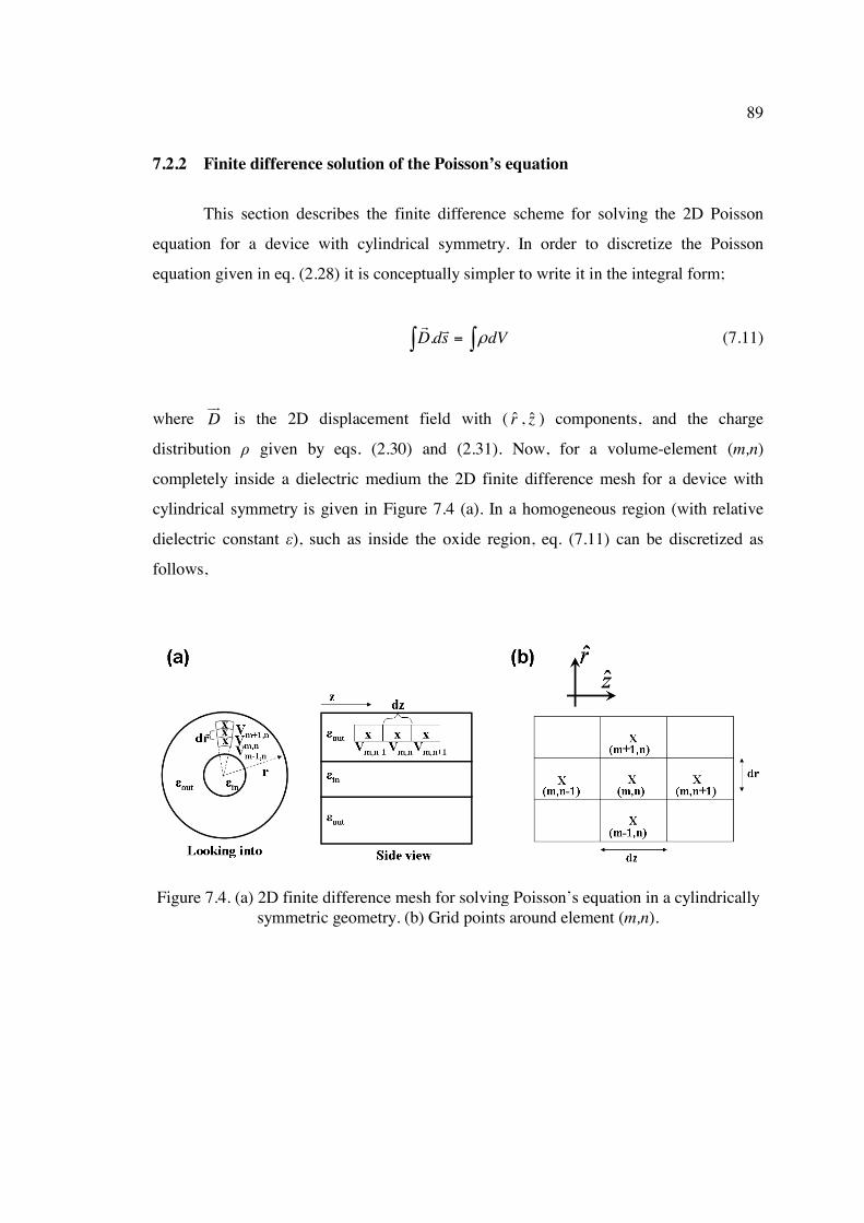
89
7.2.2 Finite difference solution of the Poisson’s equation
This section describes the finite difference scheme for solving the 2D Poisson
equation for a device with cylindrical symmetry. In order to discretize the Poisson
equation given in eq. (2.28) it is conceptually simpler to write it in the integral form;
.D ds dVρ= (7.11)
where D
is the 2D displacement field with ( r , z ) components, and the charge
distribution given by eqs. (2.30) and (2.31). Now, for a volume-element (m,n)
completely inside a dielectric medium the 2D finite difference mesh for a device with
cylindrical symmetry is given in Figure 7.4 (a). In a homogeneous region (with relative
dielectric constant ), such as inside the oxide region, eq. (7.11) can be discretized as
follows,
Figure 7.4. (a) 2D finite difference mesh for solving Poisson’s equation in a cylindrically symmetric geometry. (b) Grid points around element (m,n).

90
, 1,,
, 1,,
, , 1,
, , 1,
1, ,
2
2
122 2
m n m nm n
m n m nm n
m n m nm n
m n m nm n
Dm n m n
o o
V V drrdr
V V drrdr
V V drrdz dz
V V drrdz dz
r dr
ε
ε
ε
ε
ρπ ρ
πε πε
+
−
+
−
− + ↑
− + − ↓
− + →
− + ←
= =
(7.12)
where Vm,n is the electrostatic potential at the middle of the volume element (m,n), and
,m nρ is the net charge density in there (in units of 1/cm3). Then, due to the angular
symmetry of the device, 1Dρ is the net linear charge density along the axial direction in
units of 1/cm. In eq. (7.12) the arrows indicate the surface integral of the displacement
field, i.e. .D ds , in that direction with respect to the grid point (m,n) shown in Figure 7.4
(b). According to eqs. (2.30) and (2.31), for volume elements completely inside a given
dielectric medium ,m nρ would be zero unless there are some other charge impurities such
as oxide charges etc.
Figure 7.5. Discretization scheme at the boundary between two dielectric regions in and out. In this case mesh elements are created such that the boundary completely lies within
them.

91
The discretization scheme for a volume element at the CNT/dielectric boundary is
shown in Figure 7.5. In this case we need the potential values not only on the ‘x’ points
but also on the ‘dots’. The potential on the ‘dots’ can be approximated through finite
difference method. For example, the potential on the red dot in Figure 7.5 can be
approximated by,
, 1,3 14 4red dot m n m nV V V− += + . (7.13)
And, the final discretized form of eq. (7.11) for a mesh point (m,n) at the boundary
(Figure 7.5) can be written as,
, 1,,
, 1,,
, 1, , 1 1, 1 , 2
, 1, , 1 1, 1 ,
2
23 1 3 1 ( )4 4 4 4 4 23 1 3 14 4 4 4 4 2
m n m nout m n
m n m nin m n
out m n m n m n m n m n
out m n m n m n m n m n
V V drrdr
V V drrdr
dr drV V V V r updz
dr drV V V V rdz
ε
ε
ε
ε
+
−
+ + + +
+ − + −
− + ↑
− + − ↓
+ + − − + →
+ + − − + 2
, 1, , 1 1, 1 , 2
, 1, , 1 1, 1 , 2
1, ,
( )
3 1 3 1 ( )4 4 4 4 4 23 1 3 1 ( )4 4 4 4 4 2
122 2
in m n m n m n m n m n
in m n m n m n m n m n
Dm n m n
o o
up
dr drV V V V r downdz
dr drV V V V r downdz
r dr
ε
ε
ρπ ρ
πε πε
− + − +
− − − −
←
+ + − − − →
+ + − − − ←
= =
(7.14)
where 1Dρ (in 1/cm) corresponds to the net linear charge density along the CNT surface,
and arrows have been used in a similar notation as in eq. (7.12) and Figure 7.4 (b).

92
The non-linear procedure in solving Poisson and transport equations to achieve
self-consistency is described next. The system of equations arising from the discretization
of Poisson’s equation given by eqs. (7.12) and (7.14), along with appropriate boundary
conditions, can be put in the matrix form as,
1,1
1,2
, 1
, ,
, 1
1 1
.
m n
m n m n
m n
N N N N
V B CV
A VV
Vρ
−
+
× × ×
=
(7.15)
where, the R.H.S has the information on fixed boundary conditions and local net charge
densities. Here, N is the total number of 2D grid points. Note that in the non-linear
scheme for solving Poisson equation, the local charge density, rigorously calculated from
transport equations, is represented as a differentiable function of the local potential, i.e:
, ,( )m n m nVρ ρ= . Here, the phenomenological function is related to Vm,n through a quasi-
Fermi energy (see Appendix C of [22]). Thus, eq. (7.15) can be written in general as,
{ }( ) [ ] { } { }( )??
1 1 1 0N N NN N
F V A V Vρ× × ××
= − = (7.16)
where, { } 1NV
× is the column vector comprising electrostatic potential throughout the
discretized mesh points; i.e. V1,1, V1,2,.., etc. Then, using the Newton-Rapson method,
new potential distribution is related to the old one by,
{ } { } { }new oldV V V= + Δ (7.17)
where,

93
{ } { }( ) { }( )1
\old old
N N NV F V F V
× ×ʹ′Δ = − . (7.18)
Here, ‘\’ operator corresponds to the Gaussian elimination method for solving a linear
system of equations. In eq. (7.18) the Jaccobian matrix is given by,
{ }( ) [ ] { }( )old oldN NN N N N
F V A diag Vρ×× ×
ʹ′ ʹ′= − (7.19)
It should be noted that the last term of eq. (7.19) is a diagonal matrix of the form,
{ }( )1
2
( ) 00 ( ) 0 00 0 00 ( )
old
oldold
N N
oldN N N
VV
diag V
V
ρ
ρρ
ρ
×
×
ʹ′ ʹ′ ʹ′ =
ʹ′
(7.20)
where, ρʹ′ denotes the derivative of function ρ .

94
8. EXCITON GENERATION IN CNTS FOR OPTOELECTRONIC APPLICATIONS
This chapter describes the numerical investigation of the CNT optical emitter
reported in [10]. The modeling and simulation formalism used in this study was discussed
in the previous chapter. Here, we look into exciton generation in partially suspended CNT
transistors by the impact excitation process under high-field transport conditions. Carbon
nanotube MOSFETs with doped source/drain contacts as well as SB-CNTFETs with
metal Schottky contacts have been explored. Note that the latter type of contacts with Pd
metal were in fact used in the actual experiment [10]. This chapter is adapted from our
publications [43, 44].
The model device structures (which represent the more complex 3-dimensional
geometry of the experiment) are shown Figure 8.1. They have cylindrical symmetry with
Figure 8.1. Model device structures used in this study; (a) partially suspended CNT-MOSFET with doped source/drain contacts, (b) partially suspended SB-CNTFET with
metal Schottky contacts.
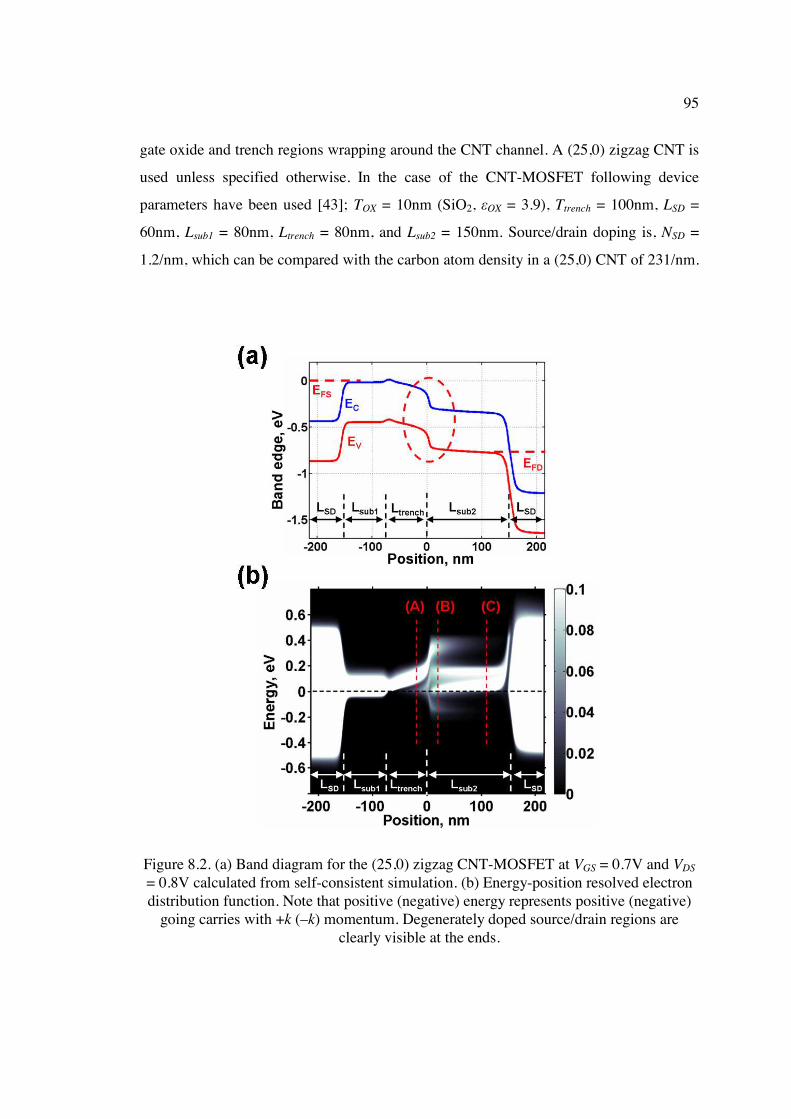
95
gate oxide and trench regions wrapping around the CNT channel. A (25,0) zigzag CNT is
used unless specified otherwise. In the case of the CNT-MOSFET following device
parameters have been used [43]; TOX = 10nm (SiO2, OX = 3.9), Ttrench = 100nm, LSD =
60nm, Lsub1 = 80nm, Ltrench = 80nm, and Lsub2 = 150nm. Source/drain doping is, NSD =
1.2/nm, which can be compared with the carbon atom density in a (25,0) CNT of 231/nm.
Figure 8.2. (a) Band diagram for the (25,0) zigzag CNT-MOSFET at VGS = 0.7V and VDS = 0.8V calculated from self-consistent simulation. (b) Energy-position resolved electron distribution function. Note that positive (negative) energy represents positive (negative)
going carries with +k (–k) momentum. Degenerately doped source/drain regions are clearly visible at the ends.
96
We use the following device parameters in the case of the SB-CNTFET [44]; TOX = 10nm
(SiO2, OX = 3.9), Ttrench = 100nm, Lsub1 = 100nm, Ltrench = 100nm, Lsub2 = 180nm, and dSB-
Metal = 10nm (Schottky barrier height, SB = 50meV).
Device operation for the partially suspended CNT-MOSFET is discussed first
(Figure 8.1 (a)). Self-consistent band diagram for this device under typical on-state
operation is shown in Figure 8.2 (a). It is clearly seen that, as suggested in [10], a
significant potential drop occurs at the trench-substrate junction near the drain-end
(dashed circle). Electrons can gain enough kinetic energy under this field, leading to a
significant hot electron population in that region. Heavily doped (n-type) source and drain
regions are also observed. This can be clearly seen in the energy-position resolved
electron distribution function shown in Figure 8.2 (b) where source/drain carrier
reservoirs are located at the two ends. In constructing Figure 8.2 (b) the energy-
momentum conversion of the phase-space distribution function, f(z,k), is accomplished
using the dispersion relation, E(k), in eq. (7.2). The direction of electron momentum is
given by the sign of the energy; i.e. +k (–k) momentum depicted by positive (negative)
energy. The detailed carrier evolution inside (and near) the trench region of the CNT-
MOSFET (Figure 8.2 (b)) will be elaborated below, along with the discussion for the SB-
CNTFET, since both devices behave similarly in this region (compare Figure 8.2 to
Figure 8.3).

97
In the case of the partially suspended SB-CNTFET, the self-consistent energy
band diagram under typical operation conditions is shown in Figure 8.3 (a). Device
parameters used here were given above. A characteristic Schottky barrier band profile is
clearly seen near the contacts. Furthermore, as suggested in Ref. [10], and similar to the
operation of the CNT-MOSFET (Figure 8.2 (a)), a significant potential drop occurs at the
trench-substrate junction near the drain contact (dashed circle). The band diagram
Figure 8.3. (a) Band diagram for the (25,0) SB-CNTFET at VGS = 0.8V and VDS = 0.7V calculated from self-consistent simulation. (b) Energy-position resolved electron
distribution function for the above device. Note that positive (negative) energy represents positive (negative) going carries with +k (–k) momentum. A significant hot-electron
population is seen at the trench-substrate junction near the drain-end (Line-(B)).

98
observed here has also been inferred by recent experimental evidence [156, 157]. In the
high-field region near the drain-end of the trench, source injected electrons can gain
enough kinetic energy leading to a significant hot electron population. This can be clearly
observed in the energy-position resolved distribution function for conduction band
electrons shown in Figure 8.3 (b) (constructed similar to Figure 8.2 (b)). Inside the trench
region, as seen in Figure 8.3 (a), the carriers are gradually accelerated under the moderate
electric field. When they gain energy above the 180meV OP energy, they emit optical
phonons and start to populate the states near the bottom of the band with E 0. This is
manifested by the appearance of low energy electron occupation near Line-(A) of Figure
8.3 (b).
The distribution function at Line-(B) situated just beyond the drain-end of the
trench shows a significant population of hot carriers, and is elaborated on in Figure 8.4.
Figure 8.4. The distribution function at Line-(B) of Figure 8.3 (b) (z = 10nm). As earlier, positive (negative) energy represents positive (negative) going carries with +k (–k)
momentum. The significant population of hot-electrons in this region can scatter to empty low-energy states by the following processes: (a) OP forward emission into the +kfinal
state, (b) OP backward emission into the –kfinal state, or, (c) high-energy exciton emission that scatters electrons down to the states near the bottom of the band (E 0).

99
Here, it clearly shows the main mechanisms for carrier scattering near this region; OP and
exciton emission. The exciton emission rate by hot carriers satisfying the energy threshold
requirement is expected to be stronger (in the range of ~ 103 ps-1) [142] compared to
energy loss through phonon scattering (< 102 ps-1) [45]. Therefore, efficient exciton
emission, accompanied by OP emission, is observed in the evolution of the distribution
function in this region (Figure 8.4). By the time carriers reach Line-(C) of Figure 8.3 (b)
all the hot electrons have been thermalized by emission of phonons/excitons and give rise
to a stream of forward going carriers with energies delineated by the OP energy. Note that
OP emission near the trench-substrate junction is not expected to lead to significant self-
heating effects. This is due to effective coupling of lattice vibrations to the substrate in
this region as confirmed by previous device simulation studies for on-substrate CNT-
MOSFETs [45]. Furthermore, experimentally observed thermal light emission in metallic
CNTs is in the suspended section of tubes, while it is absent for on-substrate tubes at
comparable device currents [11, 127]. In the case of the device studied here, under very
large drive currents, thermal light emission due to carrier heating near the trench-substrate
junction could have some contribution towards optical emission, but exciton generation
process is expected to be the dominant mechanism.
The exciton generation profile along the CNT, i.e. Rexc(z) from eq. (7.10), is
shown in Figure 8.5 (a). It clearly shows the localized nature of generation near the
trench-substrate junction. Subsequent radiative recombination of these excitons leads to
localized optical emission seen in the experiment [10]. Figure 8.5 (a) also shows exciton
generation near the drain contact. This is expected from the large electric field at that
location as seen from Figure 8.3 (a). Optical emission near the drain, however, is
expected to be largely quenched because the nanotube emission yield is lower on the
oxide than from the suspended tube (possibly due to increased non-radiative decay
channels), and near the metal contacts the excitons are quenched by energy transfer to
plasmons and screening effects. Figure 8.5 (b) shows that the highest generation rate near
the trench-substrate junction is located to the right of the high-field region. This is easily

100
understood by the energy threshold requirement for exciton emission by carriers
accelerated under this field. Furthermore, it is expected to suppress the possibility of
field-induced dissociation of excitons, and improve their radiative recombination. It is
also observed that the exciton generation cannot be described by a local field-dependent
generation rate as would be necessary for a drift-diffusion solution of this problem.
Figure 8.5. (a) Steady-state exciton generation profile along the CNT for the device shown in Figure 8.3. Localized exciton generation near the trench-substrate junction is clearly observed (dashed circle). The radiative recombination of these excitons leads to
localized optical emission seen in the experiment. Additional exciton generation near the drain contact is also observed. (b) The generation profile (solid) along with the electric
field (dashed) near the trench-substrate junction. The highest generation region is located to the right of the high-field region.

101
Figure 8.6 shows the bias dependence of device characteristics; IDS vs. VGS and the
exciton generation efficiency, ( )exc ex tot DSqN Iη −= vs. VGS. In calculating the generation
efficiency, q is the electron charge, and Nex-tot is the total number of excitons generated
per second near the trench-substrate junction. Nex-tot is calculated by integrating the
spatially resolved generation rate, Rexc(z), within the interval -50nm z 120nm of
Figure 8.5 (a). We first concentrate on the results for the SiO2 substrate oxide with Ttrench
= 10nm (solid circles). A linear increase in IDS-VGS for above-threshold operation
accompanied by an exponential increase in excη vs. VGS is seen in this case. The latter
relationship also leads to an exponential increase in the localized exciton generation rate,
Nex-tot. A key experimental result [10] was the observation of an exponential increase in
light emission intensity vs. VGS with a linear increase of IDS-VGS; a relationship attributed
to the impact excitation mechanism of the optical emission in these devices. Here, we
confirm a similar relationship for the localized exciton generation rate that would lead to
the experimentally observed device characteristics.
The effect of CNT diameter (bandgap) on exciton generation efficiency is
explored in Figure 8.6 (b) by comparing the results for the (25,0) CNT to that of a (19,0)
CNT device. For the latter, all device parameters are similar to that of the (25,0) CNT
with SiO2 substrate and Ttrench = 10nm (solid circles). We also assume a Schottky barrier
height of SB = 50meV for carrier injection and the gate metal work function is chosen
such that both devices have the same threshold voltage. Therefore, we obtain similar
device currents (IDS) for both the devices. The exciton generation efficiency for the (19,0)
CNT, however, is observed to be significantly smaller (Figure 8.6 (b)). This is because of
the larger electronic bandgap for the (19,0) CNT that increases the impact excitation
energy threshold for exciton emission to 560meV. Similar behavior is also reported for
the reduction of impact ionization rate with increasing energy threshold in conventional
CNT-MOSFET devices (without the trench) [153]. For smaller diameter tubes the device
current itself could be reduced due to larger Schottky barriers for carrier injection [158].
This would further reduce the total exciton generation rate for smaller diameter CNTs.

102
Figure 8.6. (a) IDS-VGS comparison at VDS = 0.7V for a (25,0) SB-CNTFET. Device parameters used here are similar to that in Figure 8.3 (a) except for Ttrench and the
substrate oxide. TOX = 10nm, OX = 3.9 (SiO2) and OX = 16 (HfO2) have been used. A linear increase in IDS is observed above the threshold voltage. On-current is reduced for
the deeper trench due to reduced gate coupling in that region. (b) Exciton generation efficiency at the trench-substrate junction vs. VGS shows an exponential increase. Exciton generation for a (19,0) CNT device with SiO2 substrate oxide and Ttrench = 10nm (dash-
dot curve) is compared to that of the (25,0) CNT devices (see legend of (a)).

103
Device optimization schemes are discussed next. Figure 8.6 compares two
different trench depths, Ttrench = 10nm and 100nm (solid circles and dashed squares), both
with SiO2 substrate oxide. Figure 8.6 (a) shows that the deeper trench delivers a smaller
device current. This is due to the weaker gate control of the electronic bands inside the
trench region for deeper trench depths. More importantly, however, Figure 8.6 (b) shows
that the exciton generation efficiency is higher for the device with a deeper trench which
would result in higher optical emission intensities. This is due to the larger potential drop
at the trench-substrate junction for those devices leading to a hotter carrier distribution
and higher exciton generation rates. It is, however, observed that the improvement of
emission efficiency with increasing trench depth has a saturation type behavior due to
increased electrostatic screening effects inside the trench region [43]. Therefore,
performance improvements attainable with deeper trench geometries could be limited
[43].
Figure 8.6 also compares the effect of high-k substrate oxides on device
characteristics, i.e. SiO2 (solid circles) vs. HfO2 (dotted stars). It is seen that the current
drive for the two structures is nearly equal since the device current is mainly determined
by the modulation of the channel barrier inside the trench region; in this case, both
devices have Ttrench = 10nm. On the other hand, the exciton generation efficiency for the
latter device is significantly larger than that for SiO2. This is due to the stronger gate
coupling in the substrate region for the high-k oxide that leads to a larger potential drop at
the trench-substrate junction (see Figure 8.3 (a)). This results in a hotter carrier
distribution in that region and enhancement of exciton emission efficiency. Therefore,
high-k substrate oxides could lead to significant improvement of optical emission
intensity. It is noted that the emission efficiency could be further enhanced by using a
deeper trench along with high-k oxides.
In summary, we have presented detailed numerical simulations of the partially
suspended CNT optoelectronic device reported in Ref. [10]. As observed in the

104
experiment, our simulations show localized exciton generation by hot carriers, and an
exponential increase in emission rate vs. linear increase in IDS-VGS. The emission
efficiency is predicted to improve by deeper trench geometries. High-k substrate oxides
could lead to even greater performance enhancements.
105
9. CONCLUSION AND FUTURE WORK
9.1 CNT Electronics and Band-to-Band Tunneling Devices
NEGF simulation of dissipative quantum transport in CNT transistors was a major
focus of this thesis. A detailed simulation environment that models CNTs with an
atomistic pz tight-binding Hamiltonian, along with self-consistent electrostatics, was
developed. Electron-phonon scattering was treated within the deformation potential
theory, and realistic phonon modes and their e-ph coupling in CNTs were used from
force-constant calculations. Because of the use of the pz tight-binding formalism that
describes both conduction and valence bands in CNTs, transport mechanisms based on
band-to-band tunneling and phonon-assisted tunneling were captured naturally. To our
knowledge this work is the most comprehensive treatment of dissipative quantum
transport in CNT transistors to date. It allowed us to study detailed carrier transport
effects in CNT based devices in particular, and explore interesting device physics that are
important for nanoscale transistors in general. Conventional thermionic MOSFET
operation, as well as BTBT transport, was treated in a uniform simulation environment
that allowed us to identify important performance merits of each device category in
particular. A personal outlook on the future potentials for CNT based electronics is given
in section 9.3.
At this point some possible future directions for the work presented in this thesis
on BTBT based devices are envisaged. As seen from our work (Chapter 6 in particular),
the p-i-n Tunnel FET geometry offers some unique performance advantages over the
conventional CNT-MOSFETs. Nevertheless, one main drawback for tunneling transistors
is the lower drive currents that limit circuit performance, especially in the presence of

106
large load capacitances such as interconnects. Therefore, further work is required to
identify optimization strategies for increasing the device current while maintaining steep
subthreshold slopes. It should comprehensively understand the dependence of various
device characteristics on device parameters such as doping density and profile, bandgap,
channel length, gate oxide, etc. Different material systems such as heterostructures that
could improve tunneling current near the source-channel junction while allowing large
VDD operation and better scaling properties should also be explored. Furthermore, circuit
level comparisons, beyond the intrinsic device metrics we have used so far, are required
for a better assessment of the p-i-n Tunnel FET technology over the conventional CNT-
MOSFETs. And, device optimization strategies for the best circuit level performance
should be investigated.
Finally, since there is a resurgence of interest on BTBT based devices for potential
low-power technologies it is important to extend the modeling and simulation
infrastructure beyond the 1D case considered here. As a first step, an extension of the
nanoMOS program for ultra-thin body dual gate MOSFETs can be developed for BTBT
transistors by introducing a two-band effective-mass Hamiltonian similar to that used in
[80]. This model, however, would only be valid for direct bandgap semiconductors; for
technologically important silicon and SiGe, the indirect nature of the band-structure as
well as phonon assisted tunneling needs to be treated. Barring a few exceptions [107],
most of simulation studies performed on BTBT devices in conventional semiconductors,
such as silicon, rely on physical models of questionable validity (the ones available in
commercial device simulation packages such as MEDICI). This is simply due to the sheer
computational complexity involved in the rigorous treatment of phonon assisted transport
in conventional (3D) semiconductors. Because of the renewed interest in possible
technological applications for BTBT devices, it is imperative to develop simulation tools
that accurately treat phonon mediated processes in conventional material systems.

107
9.2 CNT Optoelectronic Devices
Our work on modeling and simulation of optical emission in CNT devices has
been very promising. It clearly showed that the localized optical emission seen in the
experimental devices [10] is well described by our transport simulations based on the
exciton emission model. We further explored device optimization strategies such as the
use of high-k substrate oxides and deeper trench geometries in order to improve optical
emission intensities. There are, however, a number of future directions for the work
presented in this thesis. The numerical solution procedure described in section 7.2.1 used
an explicit scheme for the discretization of the BTE operators. On the other hand, implicit
schemes are expected to have better and more stable numerical convergence properties
[155]. Therefore, introducing an implicit solution scheme in the future will be beneficial
for improving the simulation time and the ability to handle larger device sizes. In section
7.2.1, we also assumed optical phonons to be in equilibrium with the external thermal
bath (kept at room temperature). Optical phonon emission in the high-field region near
the trench-substrate junction, however, could lead to hot-phonon effects as reported in
[45]. A significant hot-phonon population can in turn increase exciton generation rate
through phonon absorption mediated processes [142]. This effect could especially
become important under large drive currents. Therefore, it will be useful to extend the
simulation procedure presented in section 7.2.1 to include hot-phonon effects as
described in [45].
Finally, we have so far only treated electron transport in the conduction band. The
experimental devices instead show ambipolar behavior, therefore requiring hole transport
in the valence band as well. Previous observations of optical emission in CNTFETs were
in fact attributed to free carrier recombination instead of the novel excitonic mechanism.
Introduction of hole transport into the BTE simulator (thus two band transport) will allow
the treatment of free carrier recombination, along with exciton emission, in one unified
simulation environment. Treating both these processes on the same footing in the future
will allow the exploration of relative importance of the two emission mechanisms under

108
different regimes of device operation. This will undoubtedly be a very useful contribution
to the scientific community, and provide a comprehensive understanding of the operation
of CNT optoelectronic devices.
9.3 Future Outlook
Since the discovery of CNTs in early 1990’s the research on their physical
properties and possible technological applications has been extensive [5]. Carrier
transport in CNTs has been well studied by many groups, and high performance
transistors that surpass silicon transistors have been experimentally demonstrated [109].
CNTs have also been an excellent “learning tool” for investigating many interesting
device physics. The ability to rigorously model and simulate CNT based devices, as
accomplished here, is due to its simplified material structure. Nevertheless, the advent of
CNTs into semiconductor technology has been hampered by a few major challenges that
are yet to be solved. These are mainly related to their synthesis and deterministic
placement in order to build large scale circuits that is imperative for technological
manufacturability.
First of all, present techniques used for the synthesis of CNTs have large
variations in tube chiralities; i.e. semiconductor vs. metallic CNTs, as well as tube
diameters, is not well controlled. Therefore, even though individual high performance
CNT based devices can be fabricated in laboratories, the controllability required for mass-
scale manufacturing is yet to be achieved. There have been some demonstrations of post-
synthesis separation techniques, but mass-scale production of CNTs with a well defined
chirality is yet to be accomplished. Another challenge is the deterministic placement of
CNTs (both in position and direction) for wafer-scale fabrication. Even though there has
been some initial success in this regard, such as directed CVD (chemical vapor
deposition) growth techniques, it still remains a major hurdle. Aforementioned
challenges, mainly related to material science aspect of IC fabrication, need to be solved

109
before ubiquitous use of CNTs in conventional electronics. Nevertheless, there might be
attractive niche markets with less stringent requirements where CNT based electronics
can have initial market penetration. One example is thin film transistors, or flexible
electronics, that could be based on CNT networks (or mats) instead of well defined
individual tubes. In the long run, other challenges pertinent to high performance IC
manufacturing can be overcome, and CNTs could one day become the technological
workhorse that silicon has had been for many decades.

110
List of References
[1] International Technology Roadmap for Semiconductors (ITRS): www.itrs.net. [2] M. T. Bohr, R. S. Chau, T. Ghani, and K. Mistry, "The High-k Solution,"
Spectrum, IEEE, vol. 44, pp. 29-35, 2007. [3] S. Iijima, "Helical microtubules of graphitic carbon," Nature, vol. 354, p. 56,
1991. [4] S. Iijima and T. Ichihashi, "Single-shell carbon nanotubes of 1-nm diameter,"
Nature, vol. 364, p. 737, 1993. [5] M. P. Anantram and F. Leonard, "Physics of carbon nanotube electronic devices,"
Reports on Progress in Physics, vol. 69, pp. 507-61, 2006. [6] T. Durkop, S. A. Getty, E. Cobas, and M. S. Fuhrer, "Extraordinary mobility in
semiconducting carbon nanotubes," Nano Letters, vol. 4, pp. 35-9, 2004. [7] X. J. Zhou, J. Y. Park, S. M. Huang, J. Liu, and P. L. McEuen, "Band structure,
phonon scattering, and the performance limit of single-walled carbon nanotube transistors," Physical Review Letters, vol. 95, p. 146805, Sep 2005.
[8] R. Saito, G. Dresselhaus, and M. S. Dresselhaus, Physical Property of Carbon Nanotubes. London: Imperial College Press, 1998.
[9] J. A. Misewich, R. Martel, P. Avouris, J. C. Tsang, S. Heinze, and J. Tersoff, "Electrically induced optical emission from a carbon nanotube FET," Science, vol. 300, pp. 783-786, May 2003.
[10] J. Chen, V. Perebeinos, M. Freitag, J. Tsang, Q. Fu, J. Liu, and P. Avouris, "Bright infrared emission from electrically induced excitons in carbon nanotubes," Science, vol. 310, pp. 1171-1174, Nov 2005.
[11] D. Mann, Y. K. Kato, A. Kinkhabwala, E. Pop, J. Cao, X. R. Wang, L. Zhang, Q. Wang, J. Guo, and H. J. Dai, "Electrically driven thermal light emission from individual single-walled carbon nanotubes," Nature Nanotechnology, vol. 2, pp. 33-38, Jan 2007.
[12] P. Avouris, J. Chen, M. Freitag, V. Perebeinos, and J. C. Tsang, "Carbon nanotube optoelectronics," Physica Status Solidi B-Basic Solid State Physics, vol. 243, pp. 3197-3203, Nov 2006.
[13] A. Javey, J. Guo, Q. Wang, M. Lundstrom, and H. J. Dai, "Ballistic carbon nanotube field-effect transistors," Nature, vol. 424, pp. 654-657, Aug 2003.
[14] A. Javey, J. Guo, D. B. Farmer, Q. Wang, E. Yenilmez, R. G. Gordon, M. Lundstrom, and H. J. Dai, "Self-aligned ballistic molecular transistors and electrically parallel nanotube arrays," Nano Letters, vol. 4, pp. 1319-1322, Jul 2004.
[15] Y. M. Lin, J. Appenzeller, Z. H. Chen, Z. G. Chen, H. M. Cheng, and P. Avouris, "High-performance dual-gate carbon nanotube FETs with 40-nm gate length," IEEE Electron Device Letters, vol. 26, pp. 823-825, Nov 2005.
111
[16] Z. Zhang, X. Liang, S. Wang, K. Yao, Y. Hu, Y. Zhu, Q. Chen, W. Zhou, Y. Li, Y. Yao, J. Zhang, and L. M. Peng, "Doping-Free Fabrication of Carbon Nanotube Based Ballistic CMOS Devices and Circuits," Nano Lett., vol. 7, pp. 3603-3607, 2007.
[17] Y. Zhen, C. L. Kane, and C. Dekker, "High-field electrical transport in single-wall carbon nanotubes," Physical Review Letters, vol. 84, pp. 2941-4, 2000.
[18] A. Javey, J. Guo, M. Paulsson, Q. Wang, D. Mann, M. Lundstrom, and H. J. Dai, "High-field quasiballistic transport in short carbon nanotubes," Physical Review Letters, vol. 92, p. 4, Mar 2004.
[19] J. Y. Park, S. Rosenblatt, Y. Yaish, V. Sazonova, H. Ustunel, S. Braig, T. A. Arias, P. W. Brouwer, and P. L. McEuen, "Electron-phonon scattering in metallic single-walled carbon nanotubes," Nano Letters, vol. 4, pp. 517-520, Mar 2004.
[20] S. Datta, Electronic Transport in Mesoscopic Systems. Cambridge, U.K: Cambridge University Press, 1995.
[21] S. Datta, Quantum Transport: Atom to Transistor. Cambridge, U.K: Cambridge University Press, 2005.
[22] R. Lake, G. Klimeck, R. C. Bowen, and D. Jovanovic, "Single and multiband modeling of quantum electron transport through layered semiconductor devices," Journal of Applied Physics, vol. 81, pp. 7845-69, 1997.
[23] M. P. Anantram, M. S. Lundstrom, and D. E. Nikonov, "Modeling of Nanoscale Devices," http://arxiv.org/abs/cond-mat/0610247.
[24] M. Lundstrom, Fundamentals of Carrier Transport, 2 ed. Cambridge, U.K: Cambridge University Press, 2000.
[25] C. Jacoboni and L. Reggiani, "The Monte Carlo method for the solution of charge transport in semiconductors with applications to covalent materials," Reviews of Modern Physics, vol. 55, p. 645, 1983.
[26] M. V. Fischetti and S. E. Laux, "Monte carlo analysis of electron transport in small semiconductor devices including band-structure and space-charge effects," Physical Review B, vol. 38, p. 9721, 1988.
[27] A. Svizhenko and M. P. Anantram, "Role of scattering in nanotransistors," IEEE Transactions on Electron Devices, vol. 50, pp. 1459-1466, 2003.
[28] S. Jin, Y. J. Park, and H. S. Min, "A three-dimensional simulation of quantum transport in silicon nanowire transistor in the presence of electron-phonon interactions," Journal of Applied Physics, vol. 99, pp. 123719-1, 2006.
[29] E. V. Anda and F. Flores, "The role of inelastic scattering in resonant tunnelling heterostructures," Journal of Physics: Condensed Matter, vol. 3, pp. 9087-101, 1991.
[30] R. Venugopal, M. Paulsson, S. Goasguen, S. Datta, and M. S. Lundstrom, "A simple quantum mechanical treatment of scattering in nanoscale transistors," Journal of Applied Physics, vol. 93, pp. 5613-5625, 2003.
[31] J. Wang, E. Polizzi, and M. Lundstrom, "A three-dimensional quantum simulation of silicon nanowire transistors with the effective-mass approximation," Journal of Applied Physics, vol. 96, pp. 2192-2203, 2004.
112
[32] J. Guo, S. Datta, M. Lundstrom, and M. P. Anantram, "Toward Multiscale Modeling of Carbon Nanotube Transistors " International Journal for Multiscale Computational Engineering, vol. 2, p. 60, 2004.
[33] S. Hasan, PhD Thesis: Purdue University, West Lafayette, IN, 2007. [34] S. O. Koswatta, S. Hasan, M. S. Lundstrom, M. P. Anantram, and D. E. Nikonov,
"Ballisticity of nanotube field-effect transistors: Role of phonon energy and gate bias," Applied Physics Letters, vol. 89, p. 023125, Jul 2006.
[35] S. O. Koswatta, S. Hasan, M. S. Lundstrom, M. P. Anantram, and D. E. Nikonov, "Non-equilibrium Green's function treatment of phonon scattering in carbon nanotube transistors," IEEE Transactions on Electron Devices vol. 54, pp. 2339-2351, 2007.
[36] S. O. Koswatta, M. S. Lundstrom, M. P. Anantram, and D. E. Nikonov, "Simulation of phonon-assisted band-to-band tunneling in carbon nanotube field-effect transistors," Applied Physics Letters, vol. 87, p. 253107, Dec 2005.
[37] S. O. Koswatta, D. E. Nikonov, and M. S. Lundstrom, "Computational study of carbon nanotube p-i-n tunnel FETs," Technical Digest - International Electron Devices Meeting, IEDM, pp. 518-521, 2005.
[38] S. O. Koswatta, M. S. Lundstrom, and D. E. Nikonov, "Band-to-Band Tunneling in a Carbon Nanotube Metal-Oxide-Semiconductor Field-Effect Transistor Is Dominated by Phonon-Assisted Tunneling," Nano Lett., vol. 7, pp. 1160-1164, 2007.
[39] S. O. Koswatta, M. S. Lundstrom, and D. E. Nikonov, "Influence of phonon scattering on the performance of p-i-n band-to-band tunneling transistors," Applied Physics Letters, vol. 92, p. 043125, 2008.
[40] S. O. Koswatta, M. S. Lundstrom, and D. E. Nikonov, "Performance comparison between p-i-n tunneling transistors and conventional MOSFETs," IEEE Transactions on Electron Devices, Submitted.
[41] J. Appenzeller, Y. M. Lin, J. Knoch, and P. Avouris, "Band-to-band tunneling in carbon nanotube field-effect transistors," Physical Review Letters, vol. 93, p. 196805, Nov 2004.
[42] Y. R. Lu, S. Bangsaruntip, X. R. Wang, L. Zhang, Y. Nishi, and H. J. Dai, "DNA functionalization of carbon nanotubes for ultrathin atomic layer deposition of high kappa dielectrics for nanotube transistors with 60 mV/decade switching," Journal of the American Chemical Society, vol. 128, pp. 3518-3519, Mar 2006.
[43] S. O. Koswatta, V. Perebeinos, M. S. Lundstrom, and P. Avouris, "Exciton generation in suspended carbon nanotube FETs: a computational study," Technical Digest - International Electron Devices Meeting, IEDM, pp. 748-754, 2007.
[44] S. O. Koswatta, V. Perebeinos, M. S. Lundstrom, and P. Avouris, "Computational study of exciton generation in suspended carbon nanotube transistors," Nano Lett., Submitted.
[45] S. Hasan, M. A. Alam, and M. S. Lundstrom, "Simulation of Carbon Nanotube FETs Including Hot-Phonon and Self-Heating Effects," IEEE Transactions on Electron Devices, vol. 54, pp. 2352-2361, 2007.

113
[46] M. Freitag, J. Chen, J. Tersoff, J. C. Tsang, Q. Fu, J. Liu, and P. Avouris, "Mobile ambipolar domain in carbon-nanotube infrared emitters," Physical Review Letters, vol. 93, p. 076803, Aug 2004.
[47] S. Frank, P. Poncharal, Z. L. Wang, and W. A. De Heer, "Carbon nanotube quantum resistors," Science, vol. 280, pp. 1744-6, 1998.
[48] J. Kong, E. Yenilmez, T. W. Tombler, W. Kim, H. J. Dai, R. B. Laughlin, L. Liu, C. S. Jayanthi, and S. Y. Wu, "Quantum interference and ballistic transmission in nanotube electron waveguides," Physical Review Letters, vol. 8710, pp. art. no.-106801, Sep 2001.
[49] R. Venugopal, Z. Ren, S. Datta, M. S. Lundstrom, and D. Jovanovic, "Simulating quantum transport in nanoscale transistors: Real versus mode-space approaches," Journal of Applied Physics, vol. 92, p. 3730, 2002.
[50] M. S. Lundstrom and J. Guo, Nanoscale Transistors: Device Physics, Modeling and Simulation. New York: Springer, 2005.
[51] J. Tersoff, "Schottky barrier heights and the continuum of gap states," Physical Review Letters, vol. 52, pp. 465-8, 1984.
[52] Z. Ren, PhD Thesis: Purdue University, West Lafayette, IN, 2001. [53] G. Pennington and N. Goldsman, "Semiclassical transport and phonon scattering
of electrons in semiconducting carbon nanotubes," Physical Review B, vol. 68, p. 11, Jul 2003.
[54] G. Pennington and N. Goldsman, "Low-field semiclassical carrier transport in semiconducting carbon nanotubes," Physical Review B, vol. 71, p. 12, May 2005.
[55] V. Perebeinos, J. Tersoff, and P. Avouris, "Electron-phonon interaction and transport in semiconducting carbon nanotubes," Physical Review Letters, vol. 94, p. 086802, Mar 2005.
[56] V. Perebeinos, J. Tersoff, and P. Avouris, "Mobility in semiconducting carbon nanotubes at finite carrier density," Nano Letters, vol. 6, pp. 205-208, Feb 2006.
[57] A. Verma, M. Z. Kauser, and P. P. Ruden, "Ensemble Monte Carlo transport simulations for semiconducting carbon nanotubes," Journal of Applied Physics, vol. 97, pp. 114319-1, 2005.
[58] A. Verma, M. Z. Kauser, and P. P. Ruden, "Effects of radial breathing mode phonons on charge transport in semiconducting zigzag carbon nanotubes," Applied Physics Letters, vol. 87, p. 123101, Sep 2005.
[59] H. C. d'Honincthun, S. Galdin-Retailleau, J. See, and P. Dollfus, "Electron-phonon scattering and ballistic behavior in semiconducting carbon nanotubes," Applied Physics Letters, vol. 87, pp. 172112-1, 2005.
[60] H. Suzuura and T. Ando, "Phonons and electron-phonon scattering in carbon nanotubes," Physical Review B, vol. 65, p. 15, Jun 2002.
[61] S. V. Goupalov, "Continuum model for long-wavelength phonons in two-dimensional graphite and carbon nanotubes," Physical Review B (Condensed Matter and Materials Physics), vol. 71, pp. 85420-1, 2005.
[62] J. Kurti, G. Kresse, and H. Kuzmany, "First-principles calculations of the radial breathing mode of single-wall carbon nanotubes," Physical Review B (Condensed Matter), vol. 58, pp. 8869-72, 1998.

114
[63] D. Sanchez-Portal, E. Artacho, J. M. Soler, A. Rubio, and P. Ordejon, "Ab initio structural, elastic, and vibrational properties of carbon nanotubes," Physical Review B (Condensed Matter), vol. 59, pp. 12678-88, 1999.
[64] O. Dubay and G. Kresse, "Accurate density functional calculations for the phonon dispersion relations of graphite layer and carbon nanotubes," Physical Review B (Condensed Matter and Materials Physics), vol. 67, pp. 35401-1, 2003.
[65] G. D. Mahan, "Electron-optical phonon interaction in carbon nanotubes," Physical Review B vol. 68, pp. 125409-1, 2003.
[66] J. Jiang, R. Saito, G. G. Samsonidze, S. G. Chou, A. Jorio, G. Dresselhaus, and M. S. Dresselhaus, "Electron-phonon matrix elements in single-wall carbon nanotubes," Physical Review B (Condensed Matter and Materials Physics), vol. 72, pp. 235408-1, 2005.
[67] V. N. Popov and P. Lambin, "Intraband electron-phonon scattering in single-walled carbon nanotubes," Physical Review B, vol. 74, p. 13, Aug 2006.
[68] M. Machon, S. Reich, and C. Thomsen, "Electron-phonon coupling in carbon nanotubes," Physica Status Solidi B, vol. 243, pp. 3166-70, 2006.
[69] J. Guo and M. Lundstrom, "Role of phonon scattering in carbon nanotube field-effect transistors," Applied Physics Letters, vol. 86, p. 193103, May 2005.
[70] S. Hasan, M. A. Alam, and M. Lundstrom, "Simulation of carbon nanotube FETs including hot-phonon and self-heating effects," Technical Digest - International Electron Devices Meeting, IEDM, 2006.
[71] J. Guo, "A quantum-mechanical treatment of phonon scattering in carbon nanotube transistors," Journal of Applied Physics, vol. 98, p. 063519, Sep 2005.
[72] M. Pourfath, H. Kosina, and S. Selberherr, "Rigorous modeling of carbon nanotube transistors," Journal of Physics: Conference Series, vol. 38, pp. 29-32, 2006.
[73] M. Machon, S. Reich, H. Telg, J. Maultzsch, P. Ordejon, and C. Thomsen, "Strength of radial breathing mode in single-walled carbon nanotubes," Physical Review B (Condensed Matter and Materials Physics), vol. 71, pp. 35416-1, 2005.
[74] A. Svizhenko, M. P. Anantram, T. R. Govindan, B. Biegel, and R. Venugopal, "Two-dimensional quantum mechanical modeling of nanotransistors," Journal of Applied Physics, vol. 91, pp. 2343-54, 2002.
[75] S. O. Koswatta, N. Neophytou, D. Kienle, G. Fiori, and M. S. Lundstrom, "Dependence of DC characteristics of CNT MOSFETs on bandstructure models," IEEE Transactions on Nanotechnology, vol. 5, pp. 368-372, Jul 2006.
[76] M. Horowitz, E. Alon, D. Patil, S. Naffziger, K. Rajesh, and K. Bernstein, "Scaling, power, and the future of CMOS," Technical Digest - International Electron Devices Meeting, IEDM, p. 7 pp., 2005.
[77] Y. Taur and T. H. Ning, Fundamentals of Modern VLSI Devices. Cambridge, U.K: Cambridge University Press, 1998.
[78] J. Guo, S. Datta, and M. Lundstrom, "A numerical study of scaling issues for Schottky-Barrier carbon nanotube transistors," IEEE Transactions on Electron Devices, vol. 51, pp. 172-177, Feb 2004.

115
[79] D. L. John, L. C. Castro, J. Clifford, and D. L. Pulfrey, "Electrostatics of coaxial Schottky-barrier nanotube field-effect transistors," IEEE Transactions on Nanotechnology, vol. 2, pp. 175-180, Sep 2003.
[80] J. Knoch, S. Mantl, and J. Appenzeller, "Comparison of transport properties in carbon nanotube field-effect transistors with Schottky contacts and doped source/drain contacts," Solid-State Electronics, vol. 49, pp. 73-6, 2005.
[81] E. Ungersboeck, M. Pourfath, H. Kosina, A. Gehring, C. Byoung-Ho, P. Wan-Jun, and S. Selberherr, "Optimization of single-gate carbon-nanotube field-effect transistors," IEEE Transactions on Nanotechnology, vol. 4, pp. 533-8, 2005.
[82] M. Bockrath, D. H. Cobden, P. L. McEuen, N. G. Chopra, A. Zettl, A. Thess, and R. E. Smalley, "Single-electron transport in ropes of carbon nanotubes," Science, vol. 275, pp. 1922-5, 1997.
[83] M. Radosavljevic, S. Heinze, J. Tersoff, and P. Avouris, "Drain voltage scaling in carbon nanotube transistors," Applied Physics Letters, vol. 83, pp. 2435-2437, Sep 2003.
[84] J. Appenzeller, Y. M. Lin, J. Knoch, Z. H. Chen, and P. Avouris, "Comparing carbon nanotube transistors - The ideal choice: A novel tunneling device design," IEEE Transactions on Electron Devices, vol. 52, pp. 2568-2576, Dec 2005.
[85] A. Javey, J. Guo, D. B. Farmer, Q. Wang, D. W. Wang, R. G. Gordon, M. Lundstrom, and H. J. Dai, "Carbon nanotube field-effect transistors with integrated ohmic contacts and high-k gate dielectrics," Nano Letters, vol. 4, pp. 447-450, Mar 2004.
[86] P. Y. Yu and M. Cardona, Fundamentals of Semiconductors. Berlin, Germany: Springer, 1996.
[87] F. Wang, W. Liu, Y. Wu, M. Y. Sfeir, L. Huang, J. Hone, S. O'Brien, L. E. Brus, T. F. Heinz, and Y. R. Shen, "Multiphonon Raman scattering from individual single-walled carbon nanotubes," Physical Review Letters, vol. 98, p. 047402, 2007.
[88] M. S. Dresselhaus, G. Dresselhaus, R. Saito, and A. Jorio, "Raman spectroscopy of carbon nanotubes," Physics Reports-Review Section of Physics Letters, vol. 409, pp. 47-99, Mar 2005.
[89] M. Lundstrom, "Moore's law forever?," Science, vol. 299, pp. 210-211, Jan 2003. [90] S. Banerjee, W. Richardson, J. Coleman, and A. Chatterjee, "A new three-
terminal tunnel device," IEEE Electron Device Letters, vol. ED-8, pp. 347-9, 1987.
[91] T. Baba, "Proposal for surface tunnel transistors," Japanese Journal of Applied Physics, Part 2: Letters, vol. 31, pp. 455-457, 1992.
[92] W. M. Reddick and G. A. Amaratunga, "Silicon surface tunnel transistor," Applied Physics Letters, vol. 67, p. 494, 1995.
[93] J. Koga and A. Toriumi, "Negative differential conductance at room temperature in three-terminal silicon surface junction tunneling device," Applied Physics Letters, vol. 70, p. 2138, 1997.
[94] W. Hansch, C. Fink, J. Schulze, and I. Eisele, "Vertical MOS-gated Esaki tunneling transistor in silicon," Thin Solid Films, vol. 369, pp. 387-389, 2000.

116
[95] C. Aydin, A. Zaslavsky, S. Luryi, S. Cristoloveanu, D. Mariolle, D. Fraboulet, and S. Deleonibus, "Lateral interband tunneling transistor in silicon-on-insulator," Applied Physics Letters, vol. 84, pp. 1780-1782, 2004.
[96] T. Nirschl, P. F. Wang, C. Weber, J. Sedlmeir, R. Heinrich, R. Kakoschke, K. Schrufer, J. Holz, C. Pacha, T. Schulz, M. Ostermayr, A. Olbrich, G. Georgakos, E. Ruderer, W. Hansch, and D. Schmitt-Landsiedel, "The Tunneling Field Effect Transistor (TFET) as an add-on for ultra-low-voltage analog and digital processes," Technical Digest - International Electron Devices Meeting, IEDM, pp. 195-198, 2004.
[97] K. R. Kim, H. H. Kim, K.-W. Song, J. I. Huh, J. D. Lee, and B.-G. Park, "Field-Induced Interband Tunneling Effect Transistor (FITET) with negative-differential transconductance and negative-differential conductance," IEEE Transactions on Nanotechnology, vol. 4, pp. 317-321, 2005.
[98] K. K. Bhuwalka, J. Schulze, and I. Eisele, "Scaling the vertical tunnel FET with tunnel bandgap modulation and gate workfunction engineering," IEEE Transactions on Electron Devices, vol. 52, pp. 909-17, 2005.
[99] Q. Zhang, W. Zhao, and A. Seabaugh, "Low-subthreshold-swing tunnel transistors," IEEE Electron Device Letters, vol. 27, pp. 297-300, 2006.
[100] A. S. Verhulst, W. G. Vandenberghe, K. Maex, and G. Groeseneken, "Tunnel field-effect transistor without gate-drain overlap," Applied Physics Letters, vol. 91, p. 053102, 2007.
[101] E.-H. Toh, G. H. Wang, L. Chan, G. Samudra, and Y.-C. Yeo, "Device physics and guiding principles for the design of double-gate tunneling field effect transistor with silicon-germanium source heterojunction," Applied Physics Letters, vol. 91, p. 243505, 2007.
[102] S. Poli, S. Reggiani, A. Gnudi, E. Gnani, and G. Baccarani, "Computational study of the ultimate scaling limits of CNT tunneling devices," IEEE Transactions on Electron Devices, vol. 55, pp. 313-321, 2008.
[103] J. Knoch, S. Mantl, and J. Appenzeller, "Impact of the dimensionality on the performance of tunneling FETs: Bulk versus one-dimensional devices," Solid-State Electronics, vol. 51, pp. 572-578, Apr 2007.
[104] G. Zhang, X. Wang, X. Li, Y. Lu, A. Javey, and H. Dai, "Carbon nanotubes: from growth, placement and assembly control to 60mV/decade and sub-60 mV/decade tunnel transistors," Technical Digest - International Electron Devices Meeting, IEDM, pp. 431-434, 2006.
[105] W. Y. Choi, B.-G. Park, J. D. Lee, and T.-J. K. Liu, "Tunneling Field-Effect Transistors (TFETs) With Subthreshold Swing (SS) Less Than 60 mV/dec," Electron Device Letters, IEEE, vol. 28, pp. 743-745, 2007.
[106] K. Alam and R. K. Lake, "Leakage and performance of zero-Schottky-barrier carbon nanotube transistors," Journal of Applied Physics, vol. 98, pp. 64307-1, 2005.
[107] C. Rivas, R. Lake, G. Klimeck, W. R. Frensley, M. V. Fischetti, P. E. Thompson, S. L. Rommel, and P. R. Berger, "Full-band simulation of indirect phonon assisted

117
tunneling in a silicon tunnel diode with delta-doped contacts," Applied Physics Letters, vol. 78, pp. 814-816, 2001.
[108] S. Sedlmaier, J. Schulze, T. Sulima, C. Fink, C. Tolksdorf, A. Bayerstadler, I. Eisele, P. F. Wang, K. Hilsenbeck, and W. Hansch, "Phonon assisted tunneling in gated p-i-n diodes," Materials Science and Engineering B: Solid-State Materials for Advanced Technology, vol. 89, pp. 116-119, 2002.
[109] J. Guo, A. Javey, H. Dai, and M. Lundstrom, "Performance analysis and design optimization of near ballistic carbon nanotube field-effect transistors," Technical Digest - International Electron Devices Meeting, IEDM, pp. 703-6, 2004.
[110] R. Chau, S. Datta, M. Doczy, B. Doyle, B. Jin, J. Kavalieros, A. Majumdar, M. Metz, and M. Radosavljevic, "Benchmarking nanotechnology for high-performance and low-power logic transistor applications," IEEE Transactions on Nanotechnology vol. 4, pp. 153-158, 2005.
[111] J. Deng and H. S. P. Wong, "Metrics for performance benchmarking of nanoscale Si and carbon nanotube FETs including device nonidealities," Electron Devices, IEEE Transactions on, vol. 53, pp. 1317-1322, 2006.
[112] A. Marchi, E. Gnani, S. Reggiani, M. Rudan, and G. Baccarani, "Investigating the performance limits of silicon-nanowire and carbon-nanotube FETs," Solid-State Electronics, vol. 50, pp. 78-85, 2006.
[113] A. Vassighi and M. Sachdev, "Thermal runaway in integrated circuits," Device and Materials Reliability, IEEE Transactions on, vol. 6, pp. 300-305, 2006.
[114] Y. Yooh, Y. Ouyang, and J. Guo, "Effect of phonon scattering on intrinsic delay and cutoff frequency of carbon nanotube FETs," IEEE Transactions on Electron Devices, vol. 53, pp. 2467-2470, Oct 2006.
[115] S. Luryi, "Quantum capacitance devices," Applied Physics Letters, vol. 52, pp. 501-503, 1988.
[116] D. L. John, L. C. Castro, and D. L. Pulfrey, "Quantum capacitance in nanoscale device modeling," Journal of Applied Physics, vol. 96, pp. 5180-4, 2004.
[117] S. Ilani, L. A. K. Donev, M. Kindermann, and P. L. McEuen, "Measurement of the quantum capacitance of interacting electrons in carbon nanotubes," Nature Physics, vol. 2, pp. 687-691, Oct 2006.
[118] P. Avouris, Z. Chen, and V. Perebeinos, "Carbon-based electronics," Nature Nanotechnology, vol. 2, pp. 605-615, 2007.
[119] L. Marty, E. Adam, L. Albert, R. Doyon, D. Menard, and R. Martel, "Exciton formation and annihilation during 1D impact excitation of carbon nanotubes," Physical Review Letters, vol. 96, pp. 136803-1, 2006.
[120] J. Guo and M. A. Alam, "Carrier transport and light-spot movement in carbon-nanotube infrared emitters," Applied Physics Letters, vol. 86, pp. 23105-1, 2005.
[121] J. Tersoff, M. Freitag, J. C. Tsang, and P. Avouris, "Device modeling of long-channel nanotube electro-optical emitter," Applied Physics Letters, vol. 86, p. 263108, Jun 2005.
[122] D. L. McGuire and D. L. Pulfrey, "A multi-scale model for mobile and localized electroluminescence in carbon nanotube field-effect transistors," Nanotechnology, vol. 17, pp. 5805-5811, Dec 2006.
118
[123] C.-T. Hsieh, D. S. Citrin, and P. P. Ruden, "Recombination-mechanism dependence of transport and light emission of ambipolar long-channel carbon-nanotube field-effect transistors," Applied Physics Letters, vol. 90, pp. 012118-3, 2007.
[124] F. Wang, G. Dukovic, L. E. Brus, and T. F. Heinz, "The optical resonances in carbon nanotubes arise from excitons," Science, vol. 308, pp. 838-841, 2005.
[125] J. Maultzsch, R. Pomraenke, S. Reich, E. Chang, D. Prezzi, A. Ruini, E. Molinari, M. S. Strano, C. Thomsen, and C. Lienau, "Exciton binding energies in carbon nanotubes from two-photon photoluminescence," Physical Review B vol. 72, pp. 241402-1, 2005.
[126] Y. Ouyang, D. Mann, H. Dai, and J. Guo, "Theoretical Investigations on Thermal Light Emission From Metallic Carbon Nanotubes," IEEE Transactions on Nanotechnology, vol. 6, pp. 682-687, 2007.
[127] X. Wang, L. Zhang, Y. Lu, H. Dai, Y. K. Kato, and E. Pop, "Electrically driven light emission from hot single-walled carbon nanotubes at various temperatures and ambient pressures," Applied Physics Letters, vol. 91, pp. 261102-3, 2007.
[128] E. Pop, D. Mann, J. Reifenberg, K. Goodson, and D. Hongjie, "Electro-thermal transport in metallic single-wall carbon nanotubes for interconnect applications," Technical Digest - International Electron Devices Meeting, IEDM, pp. 253-256, 2005.
[129] S. M. Bachilo, M. S. Strano, C. Kittrell, R. H. Hauge, R. E. Smalley, and R. B. Weisman, "Structure-assigned optical spectra of single-walled carbon nanotubes," Science, vol. 298, pp. 2361-6, 2002.
[130] R. Pomraenke, J. Maultzsch, S. Reich, E. Chang, D. Prezzi, A. Ruini, E. Molinari, M. S. Strano, C. Thomsen, and C. Lienau, "Two-photon photoluminescence and exciton binding energies in single-walled carbon nanotubes," Physica Status Solidi B, vol. 243, pp. 2428-35, 2006.
[131] H. Hirori, K. Matsuda, Y. Miyauchi, S. Maruyama, and Y. Kanemitsu, "Exciton localization of single-walled carbon nanotubes revealed by femtosecond excitation correlation spectroscopy," Physical Review Letters, vol. 97, pp. 257401-1, 2006.
[132] O. J. Korovyanko, C. X. Sheng, Z. V. Vardeny, A. B. Dalton, and R. H. Baughman, "Ultrafast spectroscopy of excitons in single-walled carbon nanotubes," Physical Review Letters, vol. 92, pp. 017403-1, 2004.
[133] Y. Miyauchi and S. Maruyama, "Identification of an excitonic phonon sideband by photoluminescence spectroscopy of single-walled carbon-13 nanotubes," Physical Review B (Condensed Matter and Materials Physics), vol. 74, pp. 35415-1, 2006.
[134] G. N. Ostojic, S. Zaric, J. Kono, V. C. Moore, R. H. Hauge, and R. E. Smalley, "Stability of high-density one-dimensional excitons in carbon nanotubes under high laser excitation," Physical Review Letters, vol. 94, pp. 097401-1, 2005.
[135] F. Plentz, H. B. Ribeiro, A. Jorio, M. S. Strano, and M. A. Pimenta, "Direct experimental evidence of exciton-phonon bound states in carbon nanotubes," Physical Review Letters, vol. 95, pp. 247401-1, 2005.

119
[136] X. H. Qiu, M. Freitag, V. Perebeinos, and P. Avouris, "Photoconductivity spectra of single-carbon nanotubes: Implications on the nature of their excited states," Nano Letters, vol. 5, pp. 749-752, Apr 2005.
[137] A. P. Shreve, E. H. Haroz, S. M. Bachilo, R. B. Weisman, S. Tretiak, S. Kilina, and S. K. Doorn, "Determination of exciton-phonon coupling elements in single-walled carbon nanotubes by Raman overtone analysis," Physical Review Letters, vol. 98, pp. 037405-1, 2007.
[138] W. Zhenjia, H. Pedrosa, T. Krauss, and L. Rothberg, "Determination of the exciton binding energy in single-walled carbon nanotubes," Physical Review Letters, vol. 96, pp. 047403-1, 2006.
[139] V. Perebeinos, J. Tersoff, and P. Avouris, "Scaling of excitons in carbon nanotubes," Physical Review Letters, vol. 92, p. 257402, Jun 2004.
[140] V. Perebeinos, J. Tersoff, and P. Avouris, "Radiative lifetime of excitons in carbon nanotubes," Nano Letters, vol. 5, pp. 2495-2499, Dec 2005.
[141] V. Perebeinos, J. Tersoff, and P. Avouris, "Effect of exciton-phonon coupling in the calculated optical absorption of carbon nanotubes," Physical Review Letters, vol. 94, p. 027402, Jan 2005.
[142] V. Perebeinos and P. Avouris, "Impact excitation by hot carriers in carbon nanotubes," Physical Review B, vol. 74, p. 121410, Sep 2006.
[143] C. D. Spataru, S. Ismail-Beigi, L. X. Benedict, and S. G. Louie, "Excitonic effects and optical spectra of single-walled carbon nanotubes," Physical Review Letters, vol. 92, pp. 077402-1, 2004.
[144] C. D. Spataru, S. Ismail-Beigi, R. B. Capaz, and S. G. Louie, "Theory and ab initio calculation of radiative lifetime of excitons in semiconducting carbon nanotubes," Physical Review Letters, vol. 95, pp. 247402-1, 2005.
[145] E. Chang, G. Bussi, A. Ruini, and E. Molinari, "Excitons in carbon nanotubes: an ab initio symmetry-based approach," Physical Review Letters, vol. 92, pp. 196401-1, 2004.
[146] H. Zhao and S. Mazumdar, "Electron-electron interaction effects on the optical excitations of semiconducting single-walled carbon nanotubes," Physical Review Letters, vol. 93, pp. 157402-1, 2004.
[147] J. Jiang, R. Saito, G. G. Samsonidze, A. Jorio, S. G. Chou, G. Dresselhaus, and M. S. Dresselhaus, "Chirality dependence of exciton effects in single-wall carbon nanotubes: tight-binding model," Physical Review B (Condensed Matter and Materials Physics), vol. 75, pp. 35407-1, 2007.
[148] C. L. Kane and E. J. Mele, "Ratio problem in single carbon nanotube fluorescence spectroscopy," Physical Review Letters, vol. 90, pp. 207401-1, 2003.
[149] T. G. Pedersen, "Variational approach to excitons in carbon nanotubes," Physical Review B vol. 67, pp. 73401-1, 2003.
[150] D. F. Blossey, "Wannier exciton in an electric field. I. Optical absorption by bound and continuum states," Physical Review B vol. 2, pp. 3976-90, 1970.
[151] V. Perebeinos and P. Avouris, "Exciton Ionization, Franz-Keldysh, and Stark Effects in Carbon Nanotubes," Nano Lett., vol. 7, pp. 609-613, 2007.

120
[152] D. Jimenez, X. Cartoixa, E. Miranda, J. Sune, F. A. Chaves, and S. Roche, "A simple drain current model for Schottky-barrier carbon nanotube field effect transistors," Nanotechnology, vol. 18, p. 025201, 2007.
[153] J. Guo, M. A. Alam, and Y. Ouyang, "Subband gap impact ionization and excitation in carbon nanotube transistors," Journal of Applied Physics, vol. 101, p. 064311, 15 March 2007 2007.
[154] K. Banoo, PhD Thesis: Purdue University, West Lafayette, IN, 2000. [155] J. D. Hoffman, Numerical Methods for Engineers and Scientists, 2 ed. New York:
Marcel Dekker, Inc., 2001. [156] M. Freitag, J. C. Tsang, A. Bol, D. Yuan, J. Liu, and P. Avouris, "Imaging of the
Schottky Barriers and Charge Depletion in Carbon Nanotube Transistors," Nano Lett., vol. 7, pp. 2037-2042, 2007.
[157] Y. H. Ahn, A. W. Tsen, B. Kim, Y. W. Park, and J. Park, "Photocurrent Imaging of p-n Junctions in Ambipolar Carbon Nanotube Transistors," Nano Lett., vol. 7, pp. 3320-3323, 2007.
[158] Z. Chen, J. Appenzeller, J. Knoch, Y. M. Lin, and P. Avouris, "The Role of Metal-Nanotube Contact in the Performance of Carbon Nanotube Field-Effect Transistors," Nano Lett., vol. 5, pp. 1497-1502, 2005.