infineon ihw20n120r3 ds v02 06 en
DESCRIPTION
Infineon Ihw20n120r3 Ds v02 06 EnTRANSCRIPT

ResonantSwitchingSeriesReverseconductingIGBTwithmonolithicbodydiode
IHW20N120R3
Datasheet
IndustrialPowerControl

2
IHW20N120R3ResonantSwitchingSeries
Rev.2.6,2015-01-26
ReverseconductingIGBTwithmonolithicbodydiodeFeatures:
•Powerfulmonolithicbodydiodewithlowforwardvoltagedesignedforsoftcommutationonly•TRENCHSTOPTMtechnologyapplicationsoffers:-verytightparameterdistribution-highruggedness,temperaturestablebehavior-lowVCEsat-easyparallelswitchingcapabilityduetopositivetemperaturecoefficientinVCEsat•LowEMI•QualifiedaccordingtoJESD-022fortargetapplications•Pb-freeleadplating;RoHScompliant•CompleteproductspectrumandPSpiceModels:http://www.infineon.com/igbt/
Applications:
•Inductivecooking•Inverterizedmicrowaveovens•Resonantconverters•Softswitchingapplications
G
C
E
GC
E
KeyPerformanceandPackageParametersType VCE IC VCEsat,Tvj=25°C Tvjmax Marking PackageIHW20N120R3 1200V 20A 1.48V 175°C H20R1203 PG-TO247-3

3
IHW20N120R3ResonantSwitchingSeries
Rev.2.6,2015-01-26
TableofContents
Description . . . . . . . . . . . . . . . . . . . . . . . . . . . . . . . . . . . . . . . . . . . . . . . . . . . . . . . . . . . . . . . . . . . . . . . . 2
Table of Contents . . . . . . . . . . . . . . . . . . . . . . . . . . . . . . . . . . . . . . . . . . . . . . . . . . . . . . . . . . . . . . . . . . . 3
Maximum Ratings . . . . . . . . . . . . . . . . . . . . . . . . . . . . . . . . . . . . . . . . . . . . . . . . . . . . . . . . . . . . . . . . . . . 4
Thermal Resistance . . . . . . . . . . . . . . . . . . . . . . . . . . . . . . . . . . . . . . . . . . . . . . . . . . . . . . . . . . . . . . . . . 4
Electrical Characteristics . . . . . . . . . . . . . . . . . . . . . . . . . . . . . . . . . . . . . . . . . . . . . . . . . . . . . . . . . . . . . . 5
Electrical Characteristics Diagrams . . . . . . . . . . . . . . . . . . . . . . . . . . . . . . . . . . . . . . . . . . . . . . . . . . . . . 7
Package Drawing . . . . . . . . . . . . . . . . . . . . . . . . . . . . . . . . . . . . . . . . . . . . . . . . . . . . . . . . . . . . . . . . . . .13
Testing Conditions . . . . . . . . . . . . . . . . . . . . . . . . . . . . . . . . . . . . . . . . . . . . . . . . . . . . . . . . . . . . . . . . . .14
Revision History . . . . . . . . . . . . . . . . . . . . . . . . . . . . . . . . . . . . . . . . . . . . . . . . . . . . . . . . . . . . . . . . . . . .15
Disclaimer . . . . . . . . . . . . . . . . . . . . . . . . . . . . . . . . . . . . . . . . . . . . . . . . . . . . . . . . . . . . . . . . . . . . . . . . .15

4
IHW20N120R3ResonantSwitchingSeries
Rev.2.6,2015-01-26
MaximumRatingsForoptimumlifetimeandreliability,Infineonrecommendsoperatingconditionsthatdonotexceed80%ofthemaximumratingsstatedinthisdatasheet.
Parameter Symbol Value UnitCollector-emitter voltage VCE 1200 V
DCcollectorcurrent,limitedbyTvjmaxTC=25°CTC=100°C
IC 40.020.0
A
Pulsedcollectorcurrent,tplimitedbyTvjmax ICpuls 60.0 A
TurnoffsafeoperatingareaVCE≤1200V,Tvj≤175°C - 60.0 A
Diodeforwardcurrent,limitedbyTvjmaxTC=25°CTC=100°C
IF 40.020.0
A
Diodepulsedcurrent,tplimitedbyTvjmax IFpuls 60.0 A
Gate-emitter voltageTransientGate-emittervoltage(tp≤10µs,D<0.010) VGE
±20±25 V
PowerdissipationTC=25°CPowerdissipationTC=100°C Ptot
310.0155.0 W
Operating junction temperature Tvj -40...+175 °C
Storage temperature Tstg -55...+175 °C
Soldering temperature,wave soldering 1.6mm (0.063in.) from case for 10s 260 °C
Mounting torque, M3 screwMaximum of mounting processes: 3 M 0.6 Nm
ThermalResistance
Parameter Symbol Conditions Max.Value UnitCharacteristic
IGBT thermal resistance,junction - case Rth(j-c) 0.48 K/W
Diode thermal resistance,junction - case Rth(j-c) 0.48 K/W
Thermal resistancejunction - ambient Rth(j-a) 40 K/W

5
IHW20N120R3ResonantSwitchingSeries
Rev.2.6,2015-01-26
ElectricalCharacteristic,atTvj=25°C,unlessotherwisespecified
Valuemin. typ. max.
Parameter Symbol Conditions Unit
StaticCharacteristic
Collector-emitter breakdown voltage V(BR)CES VGE=0V,IC=0.50mA 1200 - - V
Collector-emitter saturation voltage VCEsat
VGE=15.0V,IC=20.0ATvj=25°CTvj=125°CTvj=175°C
---
1.481.701.80
1.70--
V
Diode forward voltage VF
VGE=0V,IF=20.0ATvj=25°CTvj=125°CTvj=175°C
---
1.551.701.80
1.75--
V
Gate-emitter threshold voltage VGE(th) IC=0.50mA,VCE=VGE 5.1 5.8 6.4 V
Zero gate voltage collector current ICESVCE=1200V,VGE=0VTvj=25°CTvj=175°C
--
--
100.02500.0
µA
Gate-emitter leakage current IGES VCE=0V,VGE=20V - - 100 nA
Transconductance gfs VCE=20V,IC=20.0A - 18.3 - S
Integrated gate resistor rG none Ω
ElectricalCharacteristic,atTvj=25°C,unlessotherwisespecified
Valuemin. typ. max.
Parameter Symbol Conditions Unit
DynamicCharacteristic
Input capacitance Cies - 1503 -
Output capacitance Coes - 50 -
Reverse transfer capacitance Cres - 42 -
VCE=25V,VGE=0V,f=1MHz pF
Gate charge QGVCC=960V,IC=20.0A,VGE=15V - 211.0 - nC
Internal emitter inductancemeasured 5mm (0.197 in.) fromcase
LE - 13.0 - nH
SwitchingCharacteristic,InductiveLoad
Valuemin. typ. max.
Parameter Symbol Conditions Unit
IGBTCharacteristic,atTvj=25°CTurn-off delay time td(off) - 387 - ns
Fall time tf - 25 - ns
Turn-off energy Eoff - 0.95 - mJ
Tvj=25°C,VCC=600V,IC=20.0A,VGE=0.0/15.0V,RG(on)=15.0Ω,RG(off)=15.0Ω,Lσ=180nH,Cσ=39pFLσ,CσfromFig.EEnergy losses include “tail” anddiode reverse recovery.

6
IHW20N120R3ResonantSwitchingSeries
Rev.2.6,2015-01-26
SwitchingCharacteristic,InductiveLoad
Valuemin. typ. max.
Parameter Symbol Conditions Unit
IGBTCharacteristic,atTvj=175°CTurn-off delay time td(off) - 454 - ns
Fall time tf - 84 - ns
Turn-off energy Eoff - 1.65 - mJ
Tvj=175°C,VCC=600V,IC=20.0A,VGE=0.0/15.0V,RG(on)=15.0Ω,RG(off)=15.0Ω,Lσ=180nH,Cσ=39pFLσ,CσfromFig.EEnergy losses include “tail” anddiode reverse recovery.

7
IHW20N120R3ResonantSwitchingSeries
Rev.2.6,2015-01-26
Figure 1. Collectorcurrentasafunctionofswitchingfrequency(Tj≤175°C,D=0.5,VCE=600V,VGE=0/15V,RG=15Ω)
f,SWITCHINGFREQUENCY[kHz]
IC,C
OLLECTO
RCURRENT[A]
0.01 0.1 1 10 1000
20
40
60
TC=80°
TC=110°
Figure 2. Forwardbiassafeoperatingarea(D=0,TC=25°C,Tj≤175°C;VGE=15V)
VCE,COLLECTOR-EMITTERVOLTAGE[V]
IC,C
OLLECTO
RCURRENT[A]
1 10 100 10000.1
1
10
100
tp=1µs
5µs
20µs
100µs
1ms
10ms
DC
Figure 3. Powerdissipationasafunctionofcasetemperature(Tj≤175°C)
TC,CASETEMPERATURE[°C]
Ptot ,POWERDISSIPATION[W
]
25 50 75 100 125 150 1750
50
100
150
200
250
300
350
Figure 4. Collectorcurrentasafunctionofcasetemperature(VGE≥15V,Tj≤175°C)
TC,CASETEMPERATURE[°C]
IC,C
OLLECTO
RCURRENT[A]
25 50 75 100 125 150 1750
20
40
8
IHW20N120R3ResonantSwitchingSeries
Rev.2.6,2015-01-26
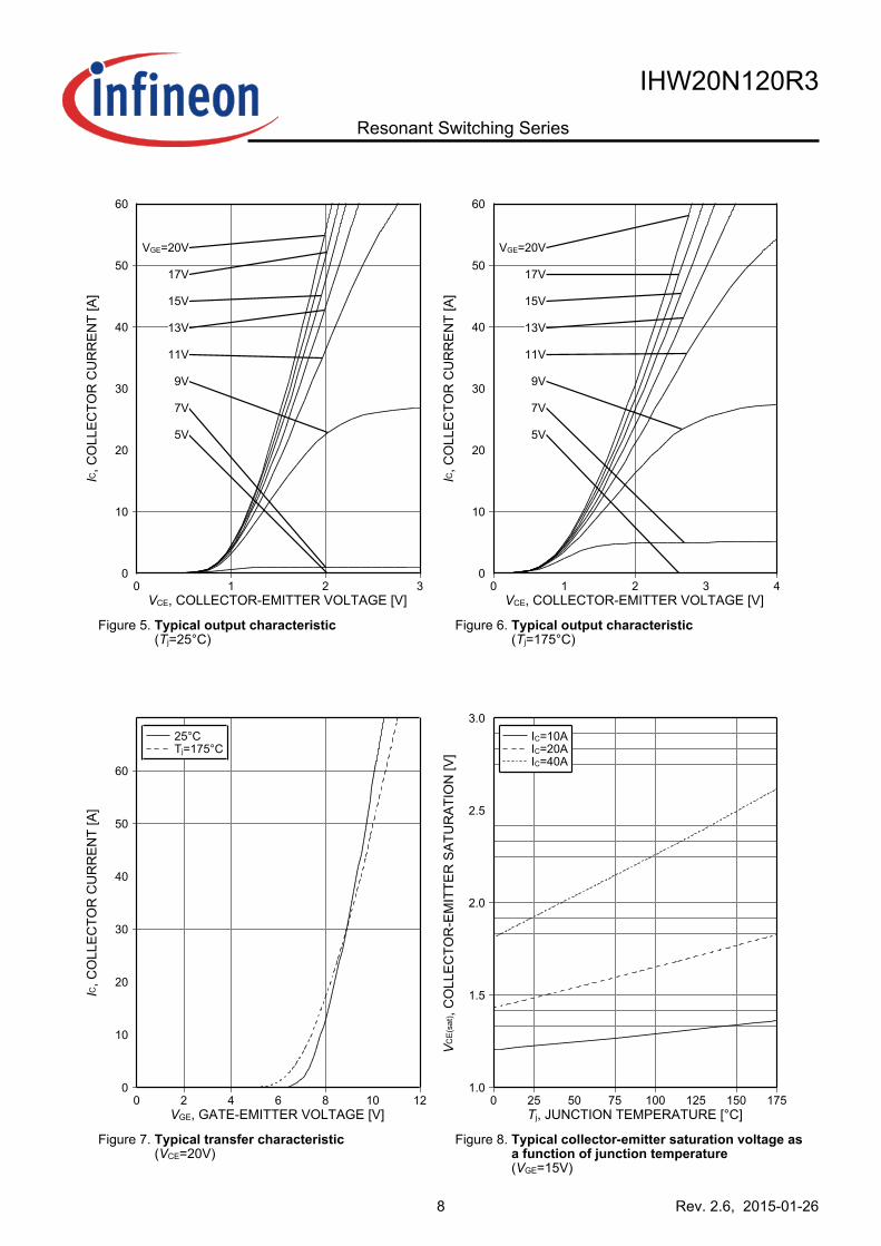
Figure 5. Typicaloutputcharacteristic(Tj=25°C)
VCE,COLLECTOR-EMITTERVOLTAGE[V]
IC,C
OLLECTO
RCURRENT[A]
0 1 2 30
10
20
30
40
50
60
VGE=20V
17V
15V
13V
11V
9V
7V
5V
Figure 6. Typicaloutputcharacteristic(Tj=175°C)
VCE,COLLECTOR-EMITTERVOLTAGE[V]
IC,C
OLLECTO
RCURRENT[A]
0 1 2 3 40
10
20
30
40
50
60
VGE=20V
17V
15V
13V
11V
9V
7V
5V
Figure 7. Typicaltransfercharacteristic(VCE=20V)
VGE,GATE-EMITTERVOLTAGE[V]
IC,C
OLLECTO
RCURRENT[A]
0 2 4 6 8 10 120
10
20
30
40
50
60
25°CTj=175°C
Figure 8. Typicalcollector-emittersaturationvoltageasafunctionofjunctiontemperature(VGE=15V)
Tj,JUNCTIONTEMPERATURE[°C]
VCE(sat) ,COLLECTO
R-EMITTE
RSATU
RATION[V
]
0 25 50 75 100 125 150 1751.0
1.5
2.0
2.5
3.0IC=10AIC=20AIC=40A
9
IHW20N120R3ResonantSwitchingSeries
Rev.2.6,2015-01-26
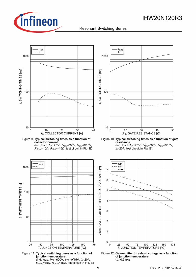
Figure 9. Typicalswitchingtimesasafunctionofcollectorcurrent(ind.load,Tj=175°C,VCE=600V,VGE=0/15V,RG(on)=15Ω,RG(off)=15Ω,testcircuitinFig.E)
IC,COLLECTORCURRENT[A]
t,SWITCHINGTIMES[ns]
0 10 20 30 4010
100
1000
td(off)
tf
Figure 10. Typicalswitchingtimesasafunctionofgateresistance(ind.load,Tj=175°C,VCE=600V,VGE=0/15V,IC=20A,testcircuitinFig.E)
RG,GATERESISTANCE[Ω]
t,SWITCHINGTIMES[ns]
10 20 30 40 5010
100
1000
td(off)
tf
Figure 11. Typicalswitchingtimesasafunctionofjunctiontemperature(ind.load,VCE=600V,VGE=0/15V,IC=20A,RG(on)=15Ω,RG(off)=15Ω,testcircuitinFig.E)
Tj,JUNCTIONTEMPERATURE[°C]
t,SWITCHINGTIMES[ns]
25 50 75 100 125 150 1751
10
100
1000td(off)
tf
Figure 12. Gate-emitterthresholdvoltageasafunctionofjunctiontemperature(IC=0.5mA)
Tj,JUNCTIONTEMPERATURE[°C]
VGE(th) ,GATE
-EMITTE
RTHRESHOLD
VOLTAGE[V
]
0 25 50 75 100 125 150 1750
1
2
3
4
5
6
7
typ.min.max.

10
IHW20N120R3ResonantSwitchingSeries
Rev.2.6,2015-01-26
Figure 13. Typicalswitchingenergylossesasafunctionofcollectorcurrent(ind.load,Tj=175°C,VCE=600V,VGE=0/15V,RG(on)=15,RG(off)=15Ω,testcircuitinFig.E)
IC,COLLECTORCURRENT[A]
E,S
WITCHINGENERGYLOSSES[m
J]
0 10 20 30 400
1
2
3 Eoff
Figure 14. Typicalswitchingenergylossesasafunctionofgateresistance(ind.load,Tj=175°C,VCE=600V,VGE=15/0V,test circuit in Fig. E)
RG,GATERESISTANCE[Ω]
E,S
WITCHINGENERGYLOSSES[m
J]
10 20 30 40 500
1
2
3Eoff
Figure 15. Typicalswitchingenergylossesasafunctionofjunctiontemperature(indload,VCE=600V,VGE=0/15V,IC=20A,RG(on)=15Ω,RG(off)=15Ω,testcircuitinFig.E)
Tj,JUNCTIONTEMPERATURE[°C]
E,S
WITCHINGENERGYLOSSES[m
J]
25 50 75 100 125 150 1750
1
2Eoff
Figure 16. Typicalswitchingenergylossesasafunctionofcollectoremittervoltage(ind.load,Tj=175°C,VGE=150/V,IC=20A,RG(on)=15Ω,RG(off)=15Ω,testcircuitinFig.E)
VCE,COLLECTOR-EMITTERVOLTAGE[V]
E,S
WITCHINGENERGYLOSSES[m
J]
400 500 600 700 800 900 10001.2
1.4
1.6
1.8
2.0
2.2Eoff

11
IHW20N120R3ResonantSwitchingSeries
Rev.2.6,2015-01-26
Figure 17. Typicalgatecharge(IC=20A)
QGE,GATECHARGE[nC]
VGE,G
ATE
-EMITTE
RVOLTAGE[V
]
0 40 80 120 160 2000.0
2.5
5.0
7.5
10.0
12.5
15.0240V960V
Figure 18. Typicalcapacitanceasafunctionofcollector-emittervoltage(VGE=0V,f=1MHz)
VCE,COLLECTOR-EMITTERVOLTAGE[V]
C,C
APACITANCE[pF]
0 10 20 3010
100
1000Cies
Coes
Cres
Figure 19. IGBTtransientthermalimpedance(D=tp/T)
tp,PULSEWIDTH[s]
ZthJC,TRANSIENTTH
ERMALIMPEDANCE[K
/W]
1E-6 1E-5 1E-4 0.001 0.01 0.1 10.001
0.01
0.1
1
D=0.5
0.2
0.1
0.05
0.02
0.01
single pulse
i:ri[K/W]:τi[s]:
19.8E-32.8E-5
20.014079934.7E-5
30.06982.0E-4
40.11581.2E-3
50.15699.9E-3
60.11370.08835259
Figure 20. Diodetransientthermalimpedanceasafunctionofpulsewidth(D=tp/T)
tp,PULSEWIDTH[s]
ZthJC,TRANSIENTTH
ERMALIMPEDANCE[K
/W]
1E-6 1E-5 1E-4 0.001 0.01 0.1 10.001
0.01
0.1
1
D=0.5
0.2
0.1
0.05
0.02
0.01
single pulse
i:ri[K/W]:τi[s]:
19.8E-32.8E-5
20.01414.7E-5
30.06982.0E-4
40.11581.2E-3
50.15699.9E-3
60.11370.08835259

12
IHW20N120R3ResonantSwitchingSeries
Rev.2.6,2015-01-26
Figure 21. Typicaldiodeforwardcurrentasafunctionofforwardvoltage
VF,FORWARDVOLTAGE[V]
IF ,FORWARDCURRENT[A]
0 1 2 30
10
20
30
40Tj=25°CTj=175°C
Figure 22. Typicaldiodeforwardvoltageasafunctionofjunctiontemperature
Tj,JUNCTIONTEMPERATURE[°C]
VF ,FO
RWARDVOLTAGE[V
]
0 25 50 75 100 125 150 1750
1
2
3IF=10AIF=20AIF=40A

13
IHW20N120R3ResonantSwitchingSeries
Rev.2.6,2015-01-26
PG-TO247-3
14
IHW20N120R3ResonantSwitchingSeries
Rev.2.6,2015-01-26
t
a b
td(off)
tf t
rtd(on)
90% IC
10% IC
90% IC
10% VGE
10% IC
t
90% VGE
t
t
90% VGE
VGE
(t)
t
t
tt1 t4
2% IC
10% VGE
2% VCE
t2 t3
E
t
t
V I toff
= x x d
1
2
CE C E
t
t
V I ton
= x x d
3
4
CE C
CC
dI /dtF
dI
I,V
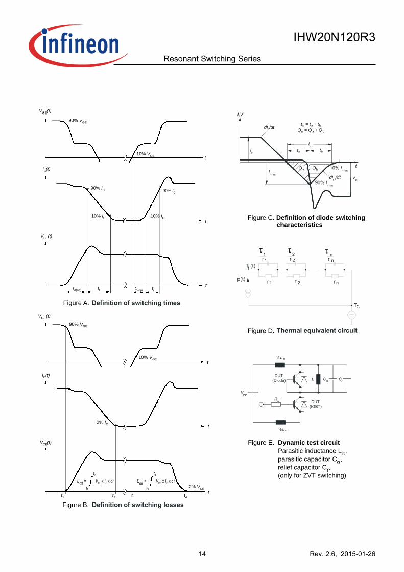
Figure A.
Figure B.
Figure C. Definition of diode switchingcharacteristics
Figure E. Dynamic test circuit
Figure D.
I (t)C
Parasitic inductance L ,
parasitic capacitor C ,
relief capacitor C ,
(only for ZVT switching)
s
s
r
t t t
Q Q Qrr a b
rr a b
= +
= +
Qa Qb
V (t)CE
VGE
(t)
I (t)C
V (t)CE
15
IHW20N120R3
Resonant Switching Series
Rev. 2.6, 2015-01-26
Revision History
IHW20N120R3
Revision: 2015-01-26, Rev. 2.6
Previous Revision
Revision Date Subjects (major changes since last revision)
1.1 2008-05-06 -
1.2 2008-07-11 -
2.3 2008-07-29 -
2.4 2009-04-01 -
2.5 2013-02-12 Layout change
2.6 2015-01-26 Minor changes
We Listen to Your CommentsAny information within this document that you feel is wrong, unclear or missing at all?Your feedback will help us to continuously improve the quality of this document.Please send your proposal (including a reference to this document) to: [email protected]
Published byInfineon Technologies AG81726 Munich, Germany81726 München, Germany© 2015 Infineon Technologies AGAll Rights Reserved.
Legal DisclaimerThe information given in this document shall in no event be regarded as a guarantee of conditions or characteristics.With respect to any examples or hints given herein, any typical values stated herein and/or any information regarding theapplication of the device, Infineon Technologies hereby disclaims any and all warranties and liabilities of any kind,including without limitation, warranties of non-infringement of intellectual property rights of any third party.
InformationFor further information on technology, delivery terms and conditions and prices, please contact the nearest InfineonTechnologies Office (www.infineon.com).
WarningsDue to technical requirements, components may contain dangerous substances. For information on the types inquestion, please contact the nearest Infineon Technologies Office.The Infineon Technologies component described in this Data Sheet may be used in life-support devices or systemsand/or automotive, aviation and aerospace applications or systems only with the express written approval of InfineonTechnologies, if a failure of such components can reasonably be expected to cause the failure of that life-support,automotive, aviation and aerospace device or system or to affect the safety or effectiveness of that device or system. Lifesupport devices or systems are intended to be implanted in the human body or to support and/or maintain and sustainand/or protect human life. If they fail, it is reasonable to assume that the health of the user or other persons may beendangered.