influence of pd thickness on micro void formation of
TRANSCRIPT

Influence of Pd Thickness on Micro Void Formation of Solder Joints in ENEPIG Surface Finish
Dong-Won Shin, Jin-Woo Heo, Yeonseop Yu, Jong-Soo Yoo, Pyoung-Woo Cheon, Seon-Hee Lee
Samsung Electro-Mechanics Co., Ltd.
Daejeon, Republic of Korea
Abstract
We investigated the micro-void formation of solder joints after reliability tests such as preconditioning (precon) and thermal cycle (TC) by varying the thickness of Palladium (Pd) in Electroless Nickel / Electroless Palladium / Immersion Gold (ENEPIG) surface finish. We used lead-free solder of Sn-1.2Ag-0.5Cu-Ni (LF35). We found multiple micro-voids of less than 10 m line up within or above the intermetallic compound (IMC) layer. The number of micro-voids increased with the palladium (Pd) layer thickness. Our results revealed that the micro-void formation should be related to (Pd, Ni)Sn4 phase re-sulted from thick Pd layer. We propose that micro-voids may form due to either entrapping of volatile gas by (Pd, Ni)Sn4 or creeping of (Pd, Ni)Sn4.
1. Introduction
There are many factors that affect the solder joint reliability in the commercial electronic packaging. Voids, especially, mi-cro-voids recently get more attention from industry because the line and space becomes finer and voids may have more po-tential to affect the solder joint reliability. Voiding in solder joint reliability heavily depends on the soleder materials and the surface finish.
In the case of solder materials, the use of lead in electronics is diminishing as the concerns on environmental issues are in-creasing. In particular, the European Union Waste Electrical and Electronic Equipment Directive (WEEE) and Restriction of Hazardous Substances Directive (RoHS) came into effect prohibiting the intentional addition of lead to most consumer elec-tronics produced in the EU in 2006. Lead-free solders may contain tin, copper, silver and traces of other metals such as bis-muth, indium, zinc and antimony. Tin-silver-copper alloys (Sn-Ag-Cu) are widely used in commercial electronic packaging.
In the surface finish, new materials have also been adopted in electronic packaging. Electroless Nickel/ Immersion Gold (ENIG) has been commonly used as a surface finish. But it has a problem in solder joint reliability, which is caused by Ni corrosion during immersion gold deposition [1-6]. ENEPIG has been applied to printed circuit board (PCB) for electronic packaging to overcome the weak point of ENIG by adding Pd layer between Ni and Au. The Pd layer is known to prevent Ni from corrosion and to act as a barrier for Ni diffusion into solder during reflow, which results in continuous IMC layer [7-11]. Another advantage of ENEPIG over ENIG is the cost reduction caused by substituting palladium for some of expen-sive gold.
Although Pd layer plays an important role in solder joint reliability, there have been a few of researches on the Pd layer, espe-cially on the optimum thickness for solder joint reliability. Among them, W.H. Wu reported that thick Pd layer had a detri-mental effect on the solder joint strength [9].
In the present study, we focused on the relation between micro-void formation and the Pd thickness among many factors for solder joint reliability. Micro-voids can have profound effect on the solder joint reliability in case that they reside around the IMC layer and form a continuous layer.
2. Experimental procedures
We prepared ENEPIG surface finish on ball grid array (BGA) circuit boards that have ball pads as depicted in Figure 1. The diameter of the pad was 300 m. The thicknesses of Ni and Au were 4.5±0.5 m and 0.14±0.04 m, respectively. We varied the thickness of the Pd layer from 0.08 to 0.32 m as summarized in Table 1.
We attached LF35 type solder balls of 250 m in diamer on the ENEPIG pads. The test specimens were reflowed in reflow oven under nitrogen atmosphere with a peak temperature of 260 C.

We carried out the precon test (85 C/85% RH/3h + reflow 3 times) and the precon followed by TC test (-55 C ~125 C, 15 min) for every test specimen.
Figure 1 - Schematic diagram of solder joint between a solder ball and ENEPIG surface finish.
Table 1 - Summary of test specimens.
Specimen Ni, m Pd, m Au, m
A 4.5±0.5 0.08±0.04 0.14±0.04
B 4.5±0.5 0.16±0.04 0.14±0.04
C 4.5±0.5 0.25±0.04 0.14±0.04
D 4.5±0.5 0.32±0.04 0.14±0.04
The test specimens were cold mounted using epoxy molding compound and cross-sectioned through a row of solder balls. They were mechanically polished with increasingly finer silicon carbide abrasive papers. The polished specimens were sometimes chemically etched using an etchant (10% hydrochloric acid + 90% methanol) to reveal the morphology of IMC.
We employed an optical microscope, a scanning electron microscope (SEM) with a field-emission gun and a focused ion beam (FIB) to analyze the micro-structure of the solder joint. We performed phase identification using energy dispersive X-ray spectroscopy (EDS) and SEM.
3. Results and Discussions
Figure 2 shows the morphology of solder joint and the composition of IMC for specimen ‘B’ after a reflow. The ratio of the atomic percentage of (Cu+Ni) to Sn in the IMC is very close to 6:5, which suggests that the phase of IMC should be (Cu,Ni)6Sn5. Micro-voids were not frequently observed before reliability tests.
Figure 2 - Cross-sectional analysis of solder joint after a reflow. (a) a SEM micrograph for specimen ‘B’, (b) an EDS
result obtained from the IMC layer indicated by the red cross in (a).

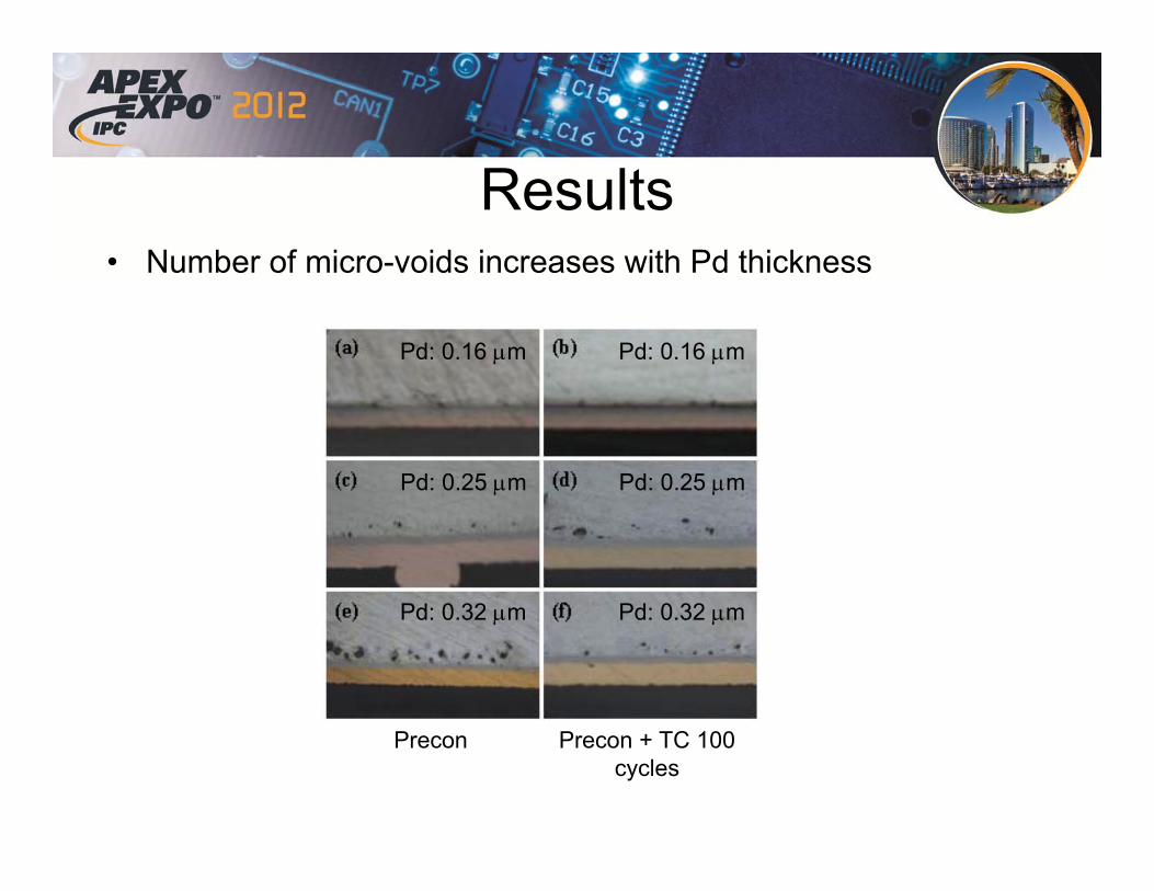
Figure 3 compares the morphological changes after reliability tests for specimen ‘B’, ‘C’ and ‘D’. It shows that the number of micro-voids increases with the Pd thickness after precon and preceon+TC 200 cycles. The micro-voids lined up at the boundary between the Ni layer and solder. The micro-voids were mostly spherical and less than 10 m in diameter.
Figure 3 - Cross-sectional optical micrographs acquired from (a) specimen ‘B’ after precon, (b) specimen ‘B’ after
precon+ TC 200 cycles, (c) specimen ‘C’ after precon, (d) specimen ‘C’ after precon+TC 100 cycles, (e) specimen ‘D’
after precon, (f) specimen ‘D’ after Precon+TC 100 cycles.
Cross-sectional FIB micrographs also indicates that there are micro-voids right above the (Cu, Ni)6Sn5 phase as shown in Figure 4(c). The micro-voids appear when the Pd thickness is greater than 0.16 m. The size of the micro-voids was less than 1 m when the Pd thickness was 0.25 m. Another important change in the morphology as the Pd thickness increases is the occurrence of another phase above (Cu, Ni)6Sn5 layer.
EDS analysis identified the phase as (Pd, Ni)Sn4 as shown in Figure 5. We observed both micro-voids and (Pd, Ni)Sn4 when the Pd layer is thicker than 0.16 m. (Pd, Ni)Sn4 phase is known to form during reflow and to be dispersed in the solder [9, 10]. The microstructure of (Pd, Ni)Sn4 is basically same as that of PdSn4, which is the phase formed in Pd-Sn diffusion couple [12, 13, 14].
Figure 4 - Cross-sectional FIB micrographs obtained from (a) specimen ‘A’ after precon+TC 100 cycles, (b) specimen
‘B’ after precon+TC 100 cycles, (c) specimen ‘C’ after precon.
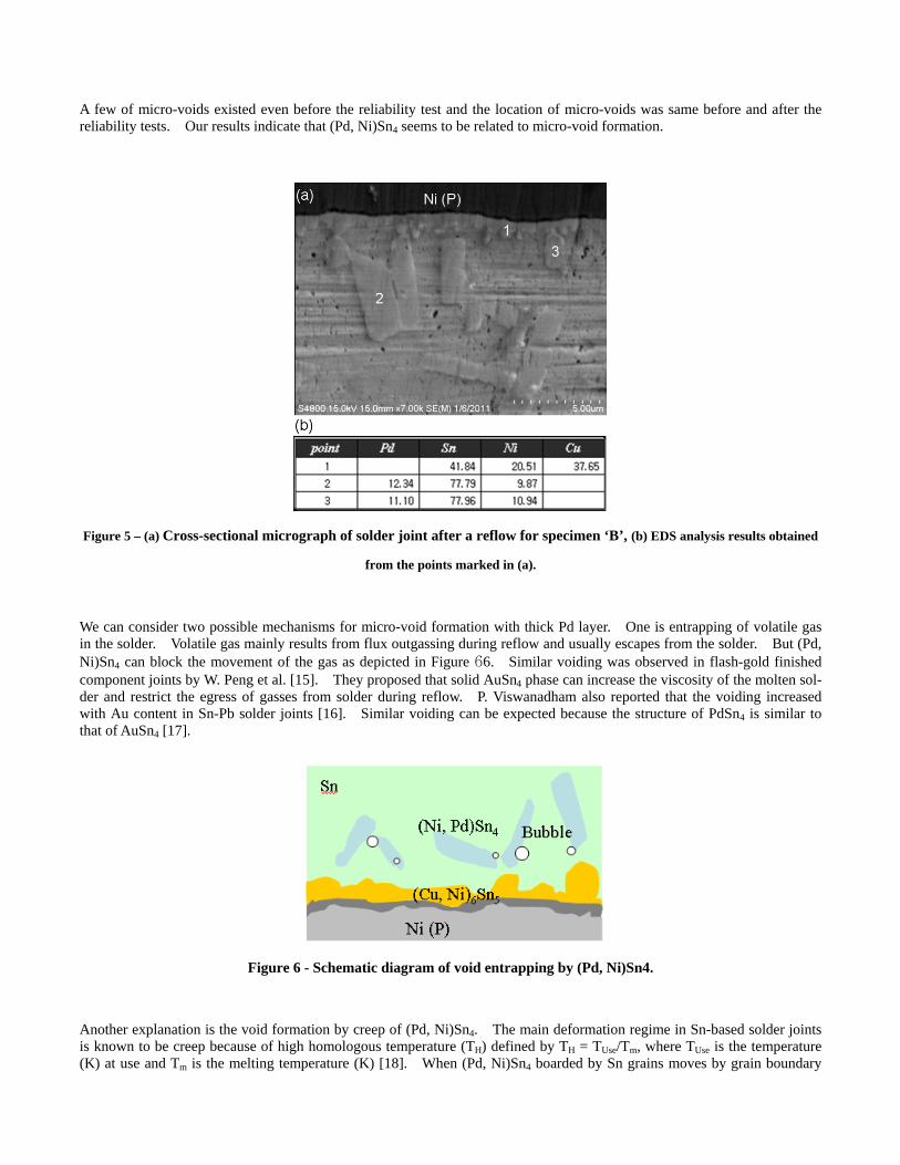
A few of micro-voids existed even before the reliability test and the location of micro-voids was same before and after the reliability tests. Our results indicate that (Pd, Ni)Sn4 seems to be related to micro-void formation.
Figure 5 – (a) Cross-sectional micrograph of solder joint after a reflow for specimen ‘B’, (b) EDS analysis results obtained
from the points marked in (a).
We can consider two possible mechanisms for micro-void formation with thick Pd layer. One is entrapping of volatile gas in the solder. Volatile gas mainly results from flux outgassing during reflow and usually escapes from the solder. But (Pd, Ni)Sn4 can block the movement of the gas as depicted in Figure 66. Similar voiding was observed in flash-gold finished component joints by W. Peng et al. [15]. They proposed that solid AuSn4 phase can increase the viscosity of the molten sol-der and restrict the egress of gasses from solder during reflow. P. Viswanadham also reported that the voiding increased with Au content in Sn-Pb solder joints [16]. Similar voiding can be expected because the structure of PdSn4 is similar to that of AuSn4 [17].
Figure 6 - Schematic diagram of void entrapping by (Pd, Ni)Sn4.
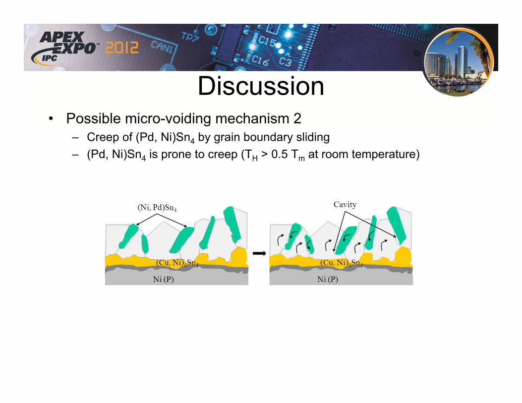
Another explanation is the void formation by creep of (Pd, Ni)Sn4. The main deformation regime in Sn-based solder joints is known to be creep because of high homologous temperature (TH) defined by TH = TUse/Tm, where TUse is the temperature (K) at use and Tm is the melting temperature (K) [18]. When (Pd, Ni)Sn4 boarded by Sn grains moves by grain boundary

sliding, voids can form at the grain boundary as described in Figure 7. Such voids are usually filled by atomic diffusion through grain boundary. But micro-voids can form in the case of cyclic deformation such as TC. Both (Pd, Ni)Sn4 and Sn can be prone to creep because their melting temperatures are relatively low considering conventional operating conditions, which ranges from 25 C to 100 C. The homologous temperature for (Pd, Ni)Sn4 at room temperature is greater than 0.5Tm because the melting temperature (Tm) is 295 C [13]. S.W. Shin reported that void nucleation and growth were caused by creep in the lead-free solders [19, 20]. V.I. Igoshev mentioned that the grain boundary sliding can cause extreme heteroge-neity of plastic deformation and lead to reduction in the polycrystal compatibility by formation of voids at grain boundaries in lead-free solders [21].
Figure 7 – Schematic diagram of voiding caused by creep of (Pd, Ni)Sn4 phase.
4. Conclusions
We investigated the effect of the Pd layer thickness in ENEPIG on the micro-void formation of the lead-free solder joint, which could be one of crucial factors for solder joint reliability. We found that (Pd, Ni)Sn4 phase and micro-voids devel-oped simultaneously as the Pd layer thickened.
This study suggests that micro-void formation is closely related to the (Pd, Ni)Sn4 phase. We conclude that the Pd layer thickness should be well controlled to avoid micro-void formation. In our particular case, the maximum thickness allowable is 0.16 m.
Reference
1. N. Niunno, Proceedings of the IPC Printed Circuits Expo. S18, 561 (1999).
2. Z. Mei, M. Kauffmann, A. Eslamnolchi and P. Johnson, 48th Electronics Components and Technology conference, 952 (1998).
3. P. Snugovsky, P. Arrowsmith and M. Romansky, J. Electron. Mater. 30, 1262 (2001).
4. R.J. Coyle, D.E.H. Popps, A. Mawer, D.P. Cullen, G.M. Wenger and P.P. Solan, IEEE Trans. Comp. Packag. Technol. 26, 724 (2003).
5. Dong-Jun Lee and Hyo S. Lee, Microelectronics and Reliability 46(7), 1119 (2006).
6. B.K. Kim, S.J. Lee, J.Y. Kim, K.Y. Ji, Y.J. Yoon, M.Y. Kim, S.H. Park and J.S. Yoo, J. Electron. Mater. 37, 527 (2008).
7. B. Kobe, N.S. McIntyre, Acta Materialia 50, 4667 (2002).
8. W. Sun, W.H. Zhu, E.S.W. Poh, H.B. Tan and R.T. Gan, Proceeding of International Conference on Electronic Packaging Technology & High Density Packaging, ICEPT-HDP, 1(2008).
9. W.H. Wu, C.S. Lin, S.H. Huang and C.E. Ho, J. Electron. Mater. 39(11), 2387 (2010).
10. S.P. Peng, W.H. Wu, C.E. Ho and Y.M. Huang, J. Alloys and Compounds 493, 431 (2010).
11. J.-W. Yoon, B.-I. Noh and S.-B. Jung, J. Electron. Mater 40(9), 1950 (2011).
12. S. Nakahara and R.J. McCoy, Thin Solid films 88, 285 (1982).
13. G. Sharma, C.M. Eichfeld and S.E. Mohney, J. Electron. Mater 32(11), 1209(2003).
14. T. Takenaka, M. Kajihara, N. Kurokawa and K. Sakamoto, Materials Science and Engineering A 406, 134 (2005).

15. W. Peng, S. Dunford, P. Viswanadham and S. Quander, 2003 Electronic Components and Technology Conference (ECTC), 809.
16. P. Viswanadham and P. Singh, Failure Modes and Mechanisms in Electronic Packages, ISBN 0-412-10591-8.
17. K.N. Tu, Materials Letters 1(1), 6(1982).
18. D.Shangguan, Lead-free solder interconnect reliability, ASM International, pp. 166-167.
19. D.K. Joo, J. Yu and S.W. Shin, J. Electron. Mater. 32(6), 541(2003).
20. S.W. Shin and J. Yu, Jpn. J. Appl. Phys. 42, 1368(2003).
21. V.I. Igosher and J.I. Kleiman, J. Electron. Mater. 29(2), 244 (2000).
Influence of Pd Thickness on Micro Void Formation of Solder Joints in
ENEPIG Surface Finish
D.-W. Shin, J.-W. Heo, Y.-S. Yu, J.-S. Yoo, P.-W. Cheon, S.-H. Lee
Samsung Electro-Mechanics Co., Ltd.

Outline
• Introduction• Methods• Results and Discussion• Summary

Introduction• Voids and reliability in solder joints
– Void formation → one of critical factors governing the reliability• Degrade mechanical strength & electrical conductivity• Location and size of voids are important in the reliability
– Industry Spec. for Voids in BGA (J-STD-001D, IPC-A-610D)• Acceptable - class 1,2,3: 25% or less voiding of the ball x-ray image area

Introduction• ENEPIG (Electroless Nickel/Electroless Palladium/Immersion Gold)
E’less Ni/Pd/Au
• Uniformed Ni thickness
• No Ni Pit and corrosion
→ High reliability
• Low cost Merit (Thinner Au)
Pd thickness is an important factor
Board
copper
Ni (P)
Gold layerPd
ENEPIG
ENIG after stripping of Au
[ Source: B.-K. Kim et al., JEM 37, 527(2008)]

Methods• Preparation of ENEPIG surface finish
– Ni: 4.5±0.5 m– Pd: 0.08, 0.16, 0.25, 0.32 ±0.04 m– Au: 0.14±0.04 m
• Attachment of solder ball and reflow– Solder: LF35 (Sn-1.2Ag-0.5Cu-Ni)– Diameter: 250 m
• Reliability tests– Precon test (85 deg. C/85% RH/3h + reflow 3 times)– Precon followed by TC test (-55 deg. C ~125 deg. C, 15 min)
• Analysis of microstructures

Results• Two kinds of intermetallic compounds
– (Cu, Ni)6Sn5, (Pd, Ni)Sn4
1
2
3
(Pd thickness: 0.16 m, after a reflow)
Results• Number of micro-voids increases with Pd thickness
Pd: 0.16 m Pd: 0.16 m
Pd: 0.25 m Pd: 0.25 m
Pd: 0.32 m Pd: 0.32 m
Precon Precon + TC 100 cycles

Results• Both micro-voids and (Pd, Ni)Sn4 phase are observed when Pd
is thicker than 0.16 m
Pd thickness is related to micro-voiding

Discussion• Possible micro-voiding mechanism 1
– Entrapping of volatile gas in the solder by blocking of (Pd, Ni)Sn4
– Source of volatile gas: flux, contaminants on ENEPIG surface
(Ni, Pd)Sn4
(Cu, Ni)6Sn5
Ni (P)
Bubble
Sn
Discussion• Possible micro-voiding mechanism 2
– Creep of (Pd, Ni)Sn4 by grain boundary sliding– (Pd, Ni)Sn4 is prone to creep (TH > 0.5 Tm at room temperature)

Summary• (Pd, Ni)Sn4 phase and micro-voids developed simultaneously
as the Pd layer thickened.• Micro-void formation is closely related to the (Pd, Ni)Sn4 phase• Pd thickness should be well controlled to avoid micro-void
formation