influence of plasma treatment on sio2/si and si3n4/si
TRANSCRIPT
1
Vol.:(0123456789)
Scientific Reports | (2021) 11:13111 | https://doi.org/10.1038/s41598-021-92432-4
www.nature.com/scientificreports
Influence of plasma treatment on SiO2/Si and Si3N4/Si substrates for large‑scale transfer of grapheneR. Lukose1*, M. Lisker1, F. Akhtar1, M. Fraschke1, T. Grabolla1, A. Mai1,2 & M. Lukosius1
One of the limiting factors of graphene integration into electronic, photonic, or sensing devices is the unavailability of large‑scale graphene directly grown on the isolators. Therefore, it is necessary to transfer graphene from the donor growth wafers onto the isolating target wafers. In the present research, graphene was transferred from the chemical vapor deposited 200 mm Germanium/Silicon (Ge/Si) wafers onto isolating (SiO2/Si and Si3N4/Si) wafers by electrochemical delamination procedure, employing poly(methylmethacrylate) as an intermediate support layer. In order to influence the adhesion properties of graphene, the wettability properties of the target substrates were investigated in this study. To increase the adhesion of the graphene on the isolating surfaces, they were pre‑treated with oxygen plasma prior the transfer process of graphene. The wetting contact angle measurements revealed the increase of the hydrophilicity after surface interaction with oxygen plasma, leading to improved adhesion of the graphene on 200 mm target wafers and possible proof‑of‑concept development of graphene‑based devices in standard Si technologies.
One of the limiting factors of graphene integration into electronic and photonic devices is the unavailability of large-scale graphene, directly grown on isolators. Therefore, for the development of graphene-based devices, graphene transfer process from the growth wafer (donor) onto the isolating (target) wafer needs to be performed. Different graphene transfer methods have been described in literature, which can be classified as dry1–6 or wet7–9 transfer methods depending on the environment the graphene is touching the target wafer during the transfer procedure. Dry graphene transfer is based on the employment of the intermediate polymer layer (e. g. PDMS stamp10) or by usage of release tape11 to avoid the direct contact of graphene with the wet solution; however, this method suffers from polymer residuals and defects like cracks, folds, and wrinkles after the transfer procedure due to the strong graphene-substrate interaction. In order to weaken it, several treatments have been investigated in the literature to ease the release of graphene from the donor wafer. Intercalation at the graphene-metal interface has also been studied in order to tune the interaction strength and to oxidize the metal surface below graphene before the graphene transfer process. For example, water intercalation12 process, where water penetrates into the graphene-metal interface for easier graphene transfer from the donor to target wafer was reported. The disad-vantage of such a method is long interaction times (16 h to up to 3 days) and low process control for wafer-scale graphene transfer. On the other hand, the intercalation with carbon monoxide13 or chemical modification14 of the graphene-metal interface to achieve higher transfer speeds has also been reported in the literature.
Another group of graphene transfer methods is based on chemical etching of the catalytic substrates on which graphene is grown. The main problem of chemical etching is metal cross-contamination, which alters the elec-trical properties of the transferred grapheme15. The alternative method of chemical etching is the wet electrical delamination process, where graphene is released from various growth substrates8,16. This method is based on the water electrolysis process, where H2 formation at the Gr-metal interface detaches graphene from the growth wafer8,16,17 and is a faster method compared to the chemical etching process. However, the electrical delamina-tion process also involves chemicals (e.g., NaOH) and poly(methyl methacrylate) (PMMA) as a support layer for graphene transfer procedure; therefore, the precise cleaning and polymer removal steps have to be understood and optimized in order to prevent the extrinsic doping of graphene. The optimized delamination process itself does not guarantee the successful transfer process, as surface contamination, hydrophilicity and roughness of target wafers also may influence the adhesion properties and respectively quality of transferred graphene.
Indeed, the 2D nature of graphene, where the ratio between the surface area to volume area is increased, leads to strong surface interactions affecting the adhesion capability compared with 3D materials. S. Das et al. reported
OPEN
1IHP- Leibniz Institut Für Innovative Mikroelektronik, Im Technologiepark 25, 15236 Frankfurt (Oder), Germany. 2Technical University of Applied Science Wildau, Hochschulring 1, 15745 Wildau, Germany. *email: [email protected]

2
Vol:.(1234567890)
Scientific Reports | (2021) 11:13111 | https://doi.org/10.1038/s41598-021-92432-4
www.nature.com/scientificreports/
the adhesion energy increase after thermal annealing procedures to improve the adhesion of graphene on SiOx18.
At this point, the hydrophilicity-hydrophobicity of the target wafers is one of the most critical parameters for the adhesion of 2D graphene; however, only very few literature works deal with this phenomenon. Kim et al.19 showed the relation between the SiO2 surface wettability and graphene quality transferred by wet transfer to reduce the content of wrinkles in graphene after the transfer on the target wafer. However, the organic solvent (instead of DI water) was used in their work, making the transfer process more complex. Another study involved aluminum nitride (AlN) surfaces, as they were investigated as a target wafers for graphene transfer20. Different surface treatments lead to increased surface wettability as detected by measured wetting contact angle (WCA) measurements between solid surface and water drop. This clearly shows the need for further investigations and understandings of the relation between surface wettability properties and therefore the adhesion of graphene on the target wafers.
In this paper, graphene was transferred by the electrochemical delamination process from 200 mm Ge/Si donor wafers on 200 mm, Si technology standard SiO2/Si and Si3N4/Si target wafers by changing their hydrophilic behavior with an additional surface treatment to achieve low-defect and up-scaled graphene transfer process. The electrochemical delamination process was selected since wafer-scale graphene transfer through wafer bonding or etching of Ge under graphene is still not achieved for Gr/Ge/Si system. In the graphene growth-transfer process, no metals (e.g., Cu, Ni, etc.) were involved; therefore, metal cross-contamination problems were avoided. In the present research, the surface wetting contact angle measurements of the target wafers and surface composition and roughness measurements by XPS and AFM were performed, respectively. The obtained results allowed us to determine the relationship between surface composition, roughness, wettability, and graphene’s adhesion ability on the target wafers with respect to additional surface treatment by oxygen plasma. Finally, the improved graphene adhesion was achieved for possible future fabrication of proof-of-concept graphene-based devices in standard Si technologies.
Results and discussionIn the present research, four different target surfaces were selected for the transfer experiments of graphene. Three types of SiO2 (HDP- SiO2, TEOS—SiO2, and thermal—SiO2) and one type of Si3N4 (PE-Si3N4) films were employed as target surfaces on standard Si wafers. To be precise, HDP stands for high-density plasma deposi-tion using silane (SiH4) precursor at 650 °C deposition temperature, TEOS is the deposition of SiO2 by using the tetraethyl(ortho)silicate (TEOS) precursor and plasma at 400 °C, whereas thermal SiO2 is produced at a temperature of 1000 °C. Si3N4 films were grown by plasma enhanced (PE) chemical vapor deposition at 400 °C by using silane and NH3/N2 gasses as precursors. For all SiO2 and Si3N4 target surfaces the graphene transfer and post-transfer processing steps were identical in order to observe the effect of target surface and dependences with respect to certain changes.
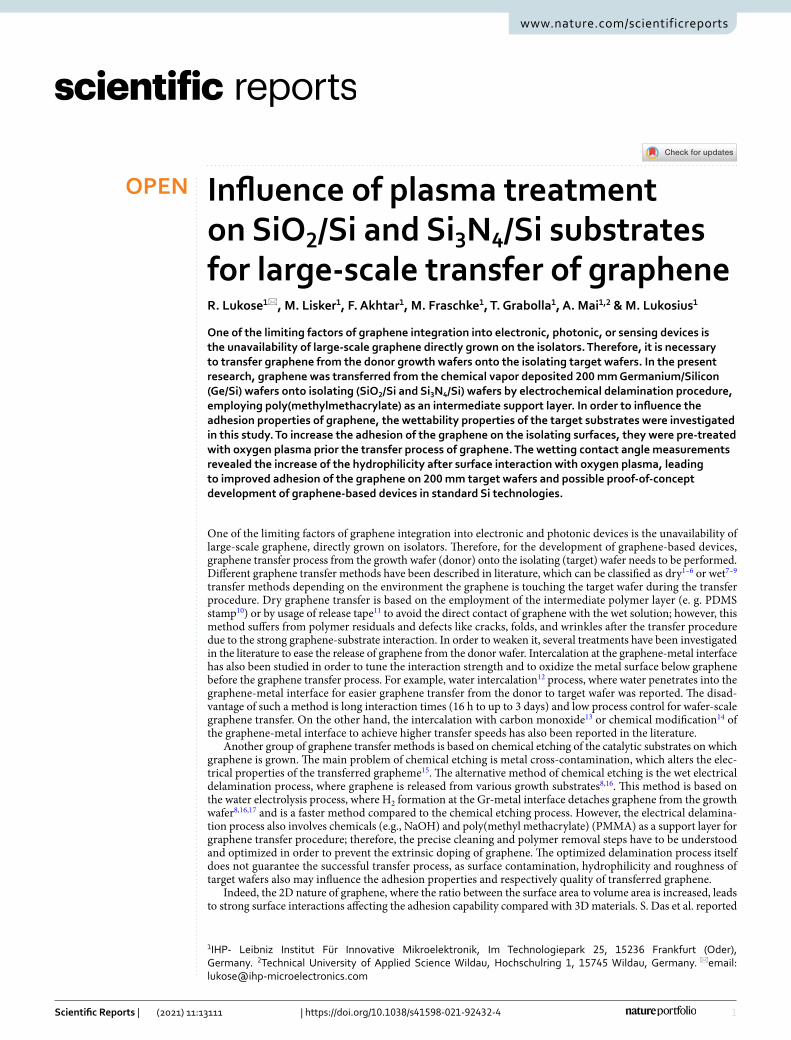
Firstly, the chemical affinity/surface reactivity of SiO2, Si3N4 target surfaces was investigated by measuring the wettability contact angle (WCA) with the sessile drop method21. By this method, the interaction and spreading of a small volume (1µL) water droplet on a solid surface is investigated. The contact angle (θ) for a flat surface is described by Young equation22 cos (θ) = (γSV−γSL)/γLV, where (γ) is the surface tension of solid–vapor (SV), solid–liquid (SL) and liquid–vapor (LV) interfaces, respectively. Theoretically, surface is hydrophilic if the contact angle between the solid surface and water is below 90°. On the hydrophilic surfaces, water tends to spread out on the material surface due to higher adsorption as binding energies between water molecules. The observed contact angles revealed the hydrophilic behavior of SiO2 and Si3N4 surfaces independently on the deposition conditions—contact angles were below 90° (Fig. 1a–c). The as-grown 100 nm SiO2 films had contact angles of 25°, 31°, and 45° for HDP- SiO2, TEOS—SiO2, and thermal—SiO2, respectively. The observed WCA values for SiO2 agrees with data reported in the literature, where the WCA varies from ca. 28° to 52°19,20,23. The WCA for as-grown 40 nm thick PE-Si3N4 films were approximately equal to 38°.
Despite the hydrophilic nature of SiO2 and Si3N4 layers, the transfer experiments on the described target wafers resulted in mechanically damaged graphene (Fig. 1d–f). The achieved quality of transferred graphene flakes was not suitable for further development of large-scale graphene-based devices; therefore, further experi-ments were performed to solve the observed transfer challenges.
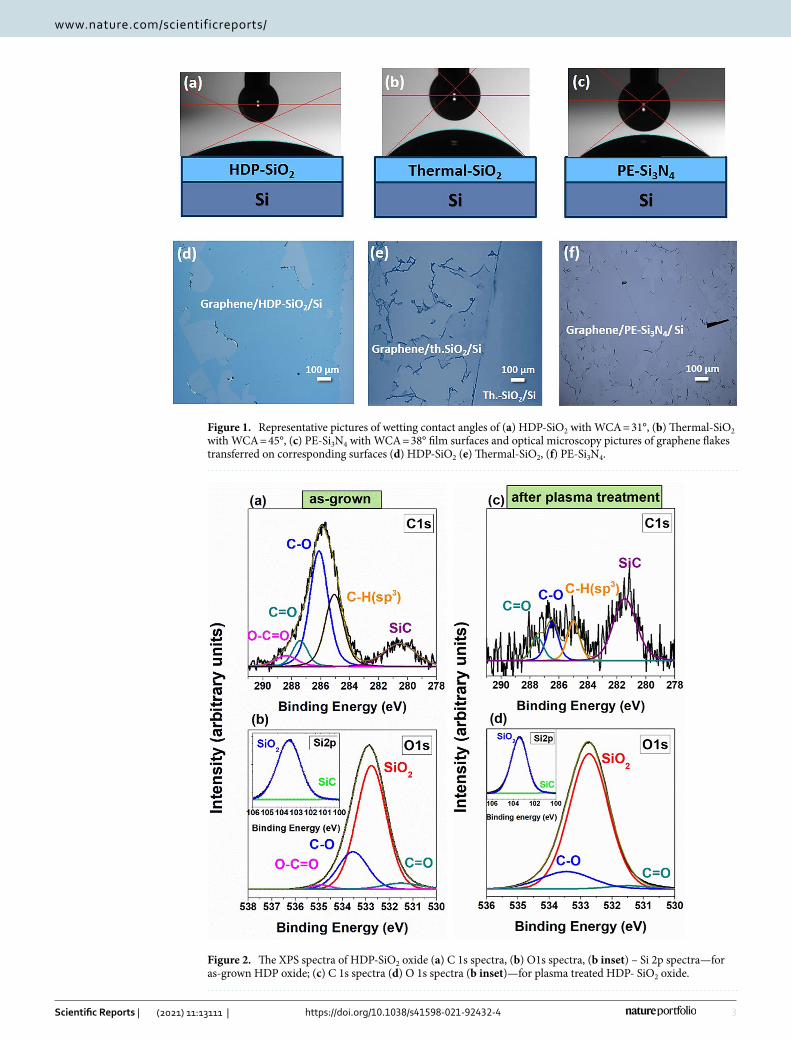
To determine if surface contamination of target wafers could be the reason for inhomogeneous graphene flake adhesion, the XPS spectroscopy measurements were performed firstly for SiO2 and lately for Si3N4 surfaces. The fitting of the C 1s peak at 286 eV revealed the characteristic peaks related to carbon-containing groups C–H, C–O, C = O, –O–C = O (Fig. 2a). This tendency was noticed for all SiO2 films; however, in the case of thermal-SiO2, the surface contamination by carbon-containing groups is lower. No functional ester group (–O–C = O) was detected, related to high process temperature (1000 °C) and therefore higher stability towards adsorption from the ambient (SI Fig. S1). Despite the different precursors and process parameters for the deposition of SiO2 films, the surface contamination was quite similar for all surfaces of investigated oxide films. Additionally, the very clear and intensive peak at the binding energies of 280.7 eV was observed, which was assigned to Si–C bonding. Similar surface contamination tendency was observed from the fitting of O 1s peak at 532.8 eV binding energy (Fig. 2b). The main peak is attributed to SiO2, however also in O1s spectra, carbon-containing organic groups were observed at the surface of the samples, including the above-mentioned C–O, C=O, –O–C=O groups for HDP- and TEOS-SiO2 (SI Fig. S1). Whereas, for thermal-SiO2, –O–C=O functional group was not observed on the surface, due to the same reasons as mentioned above in the explanation for C1s spectra.
No differences in Si 2p spectra were noticed for differently grown SiO2 films, where mainly the characteristic Si–O peak at a binding energy of 103.5 eV was detected (Fig. 2b inset and SI Fig. S1b, d, f insets). In order to reduce the content of C-containing groups on the surface of SiO2 films, the oxygen plasma treatment was applied. The XPS analysis on plasma treated SiO2/Si and Si3N4/Si surfaces revealed surface composition changes compared
3
Vol.:(0123456789)
Scientific Reports | (2021) 11:13111 | https://doi.org/10.1038/s41598-021-92432-4
www.nature.com/scientificreports/
Figure 1. Representative pictures of wetting contact angles of (a) HDP-SiO2 with WCA = 31°, (b) Thermal-SiO2 with WCA = 45°, (c) PE-Si3N4 with WCA = 38° film surfaces and optical microscopy pictures of graphene flakes transferred on corresponding surfaces (d) HDP-SiO2 (e) Thermal-SiO2, (f) PE-Si3N4.
Figure 2. The XPS spectra of HDP-SiO2 oxide (a) C 1s spectra, (b) O1s spectra, (b inset) – Si 2p spectra—for as-grown HDP oxide; (c) C 1s spectra (d) O 1s spectra (b inset)—for plasma treated HDP- SiO2 oxide.

4
Vol:.(1234567890)
Scientific Reports | (2021) 11:13111 | https://doi.org/10.1038/s41598-021-92432-4
www.nature.com/scientificreports/
to as-grown SiO2 films (Fig. 2c, d, and SI Fig. S2). For oxides, fitting of characteristic C 1s peak at 286 eV revealed the obvious reduction of corresponding C–H, C–O, –O–C=O bond peaks after plasma treatment and was mainly related to the reduction of surface contamination (Fig. 2c, and SI Fig. S2a, c, e). The functional –O–C=O group was completely removed from the surface of HDP-SiO2 films after the interaction with oxygen plasma (Fig. 2c). For the surface of TEOS-SiO2 films, the C1s spectra showed reduced surface contamination after plasma treat-ment; however, still containing all surface contaminants as before plasma treatment (SI Fig. S2c). The elongated exposer times for TEOS-SiO2 films should be applied for getting cleaner surfaces; however, the precise exposer time control is required to avoid the damaging or (and) doping of the surface. In the case of thermal-SiO2, the functional –C=O group was completely removed from the surface after plasma treatment (SI Fig. S2e). The observed Si–C peak at binding energies of 280.7 eV was not affected by plasma treatment for all SiO2 films. The fitting of the O 1s region in XPS spectra after plasma treatment (Fig. 2d and S2) showed exactly the same behavior as in the C 1s spectra. Additionally to the main SiO2 peak at 532.8 eV binding energy, carbon-containing groups were detected on as-grown SiO2 surfaces, whereas the exposer to oxygen plasma leads to a reduction of carbon-containing groups and removal of –O–C=O group for HDP-SiO2, and –C=O group for thermal-SiO2 (Fig. 2d and S2f.). In the case of TEOS-SiO2, all functional C-containing groups remained on the surface, as detected in C 1s spectra (Fig. S2d). To conclude, thermal SiO2 was produced at a higher process temperature (1000 °C), and it seems that the surface of thermal oxide is more stable compared with other oxides, leading to less C-contaminated surface and lower surface modification after oxygen plasma treatment at 250 °C. However, the plasma effect on HDP- and TEOS-SiO2 surfaces were rather similar and revealed a slight reduction in surface contamination.
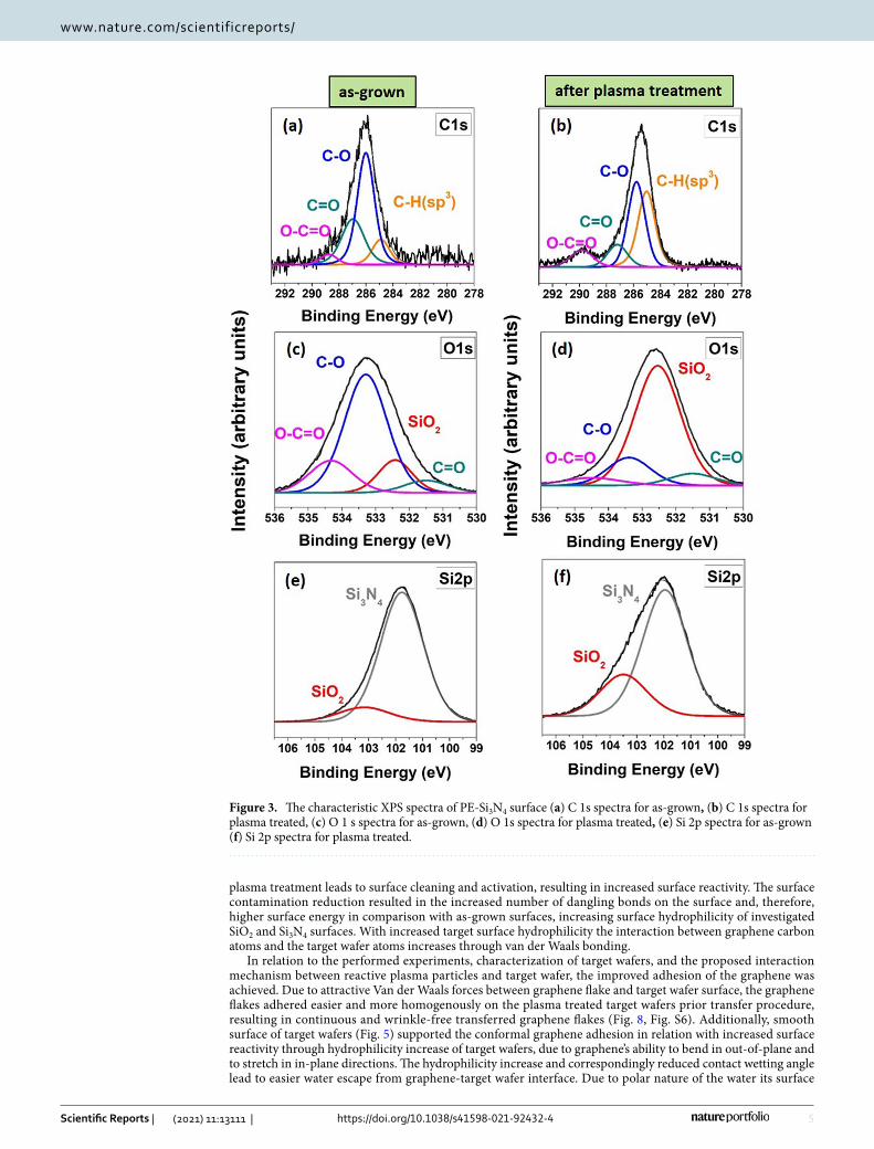
The XPS analysis was also performed for as-grown and plasma treated Si3N4/Si surface. In the characteristic C1s spectra, higher C–O peak was observed for as-grown S3N4 films (Fig. 3a) in comparison to plasma treated surface of S3N4 (Fig. 3b). Correspondingly, in the O1s spectra the intensive C–O spectra was reduced and increase of SiO2 peak was observed if the surface of as-grown S3N4 films (Fig. 3c) was treated with oxygen plasma (Fig. 3d). The slight shift in C1s and O1s spectra towards lower binding energies were observed for plasma treated surface and is related to reduction of C–O components. In Si2p spectra characteristic SiO2 peak at 103.5 eV binding energy (Fig. 3e) also increased for the plasma treated S3N4 surface (Fig. 3f). In the Si2p spectra, the intensity of the Si–O peak increases in respect to the Si–N peak, and broadening of the Si 2p (Fig. 3f) is probably due to partial exchange of N by O during the interaction of Si3N4 with plasma generated O radicals. Luhmann et al.24 also observed (from XPS) the substitution of oxygen and depletion of nitrogen at the surface of LP-CVD silicon nitride films after the exposer to oxygen plasma. Like in the SiO2 case, the plasma treatment leads to a slight reduction of C-contamination on the film surface (Fig. 3b), whereas the fitting of N1s spectra before and after plasma treatment revealed no obvious peak intensity and composition changes (SI Fig. S3).
Additionally, the XPS analysis was performed to determine if Ge cross-contamination and electrolyte residuals (NaOH) appeared after the graphene growth and transfer on the target wafer, respectively. No characteristic Na 1s and Ge 2p peaks were observed in XPS spectra for all investigated transferred graphene samples (SI Fig. S4), or the contamination level was below the detection limit. Furthermore, the possible graphene doping through the oxygen plasma treatment of target wafers was analyzed by Raman spectroscopy. No shifts in G and 2D peaks of graphene have been observed on the samples, transferred on plasma treated SiO2 and the non-treated samples (Fig. 4. for HDP-SiO2/Si). No change of 2D/G (~ 1.8) ratio was noticed for plasma treated surfaces, indicating no doping or quality reduction after plasma treatment of investigated surfaces before graphene transfer.
Furthermore, the possible plasma effect on surface roughness was analyzed by atomic force microscopy for all SiO2/Si and Si3N4/Si surfaces. The as-grown SiO2 films revealed very low surface roughness (RMS) equal to 0.14 ± 0.02, 0.17 ± 0.02, and 0.22 ± 0.04 nm for HDP-SiO2, thermal-SiO2, TEOS-SiO2 films, respectively. In literature, the RMS values vary from 0.4 to 1.9 nm for as-grown oxide films20,25,26, depending on the deposition method. The surface roughness of as-grown Si3N4 films was equal to 0.73 ± 0.06 nm (Fig. 5a); however, no obvious difference in the quality of transferred graphene was noticed in comparison to graphene transfer experiments on SiO2 shown in Fig. 1. Whereas Knapp et al.20 observed the reduction of surface roughness for plasma-treated AlN surfaces, in the present research, no obvious reduction of surface roughness was observed for Si3N4 (Fig. 5). Only minor surface roughness variation before and after plasma treatment was noticed (Fig. 5c) for CVD grown SiO2 film as well. According to Wenzel et al.27 the contact angle for rough surfaces should be extracted by including the surface roughness component [cos θm = r × cos θ]. However, in the present research, no obvious roughness and morphology changes were observed for SiO2/Si and Si3N4/Si surfaces; therefore, the film roughness effect on an absolute value of contact wetting angle was neglected for as-grown and plasma-treated target surfaces.
Finally, the WCA measurements have been performed on the plasma treated samples. It was indeed found that the surface hydrophilicity and, therefore, surface reactivity increased. The measured WCA angles for plasma-treated surfaces revealed the reduced wetting contact angles (Fig. 6), which is due to the surface purification after processing with oxygen plasma. During the plasma process most of organic bonds (i.e., C–H, C–C, C = C, C–O, C–N) of surface contaminants are broken and oxidized leading to formation of H2O, CO, CO2 et al. which are pumped out from the reaction chamber during the processing.
The measured WCA was equal to 2.4°, 2°, and 2.7° degrees for HDP-, TEOS-SiO2 and PE-Si3N4 films, respec-tively, resulting in highly hydrophilic surfaces. The determined WCA angle of 20° for thermal- SiO2 agrees with obtained XPS results (slightly affected surface composition) and confirms the relative surface stability towards oxygen plasma.
According to the obtained experimental results, a simple graphical explanation, as possible surface interac-tion and modification model after interaction with oxygen plasma, is visualized in Fig. 7. Firstly, by oxygen plasma treatment, the C-contamination is partly removed from the investigated SiO2 and Si3N4 surfaces through bombardment with active radicals and particles generated through oxygen plasma (like i.e. O2
+, O2−, O3, O, O+,
O− and free electrons). Secondly, in the case of Si3N4, oxygen from the plasma substitutes and exchanges nitro-gen in Si3N4 films, leading to the partially oxidized surfaces. As determined by XPS characterization, oxygen
5
Vol.:(0123456789)
Scientific Reports | (2021) 11:13111 | https://doi.org/10.1038/s41598-021-92432-4
www.nature.com/scientificreports/
plasma treatment leads to surface cleaning and activation, resulting in increased surface reactivity. The surface contamination reduction resulted in the increased number of dangling bonds on the surface and, therefore, higher surface energy in comparison with as-grown surfaces, increasing surface hydrophilicity of investigated SiO2 and Si3N4 surfaces. With increased target surface hydrophilicity the interaction between graphene carbon atoms and the target wafer atoms increases through van der Waals bonding.
In relation to the performed experiments, characterization of target wafers, and the proposed interaction mechanism between reactive plasma particles and target wafer, the improved adhesion of the graphene was achieved. Due to attractive Van der Waals forces between graphene flake and target wafer surface, the graphene flakes adhered easier and more homogenously on the plasma treated target wafers prior transfer procedure, resulting in continuous and wrinkle-free transferred graphene flakes (Fig. 8, Fig. S6). Additionally, smooth surface of target wafers (Fig. 5) supported the conformal graphene adhesion in relation with increased surface reactivity through hydrophilicity increase of target wafers, due to graphene’s ability to bend in out-of-plane and to stretch in in-plane directions. The hydrophilicity increase and correspondingly reduced contact wetting angle lead to easier water escape from graphene-target wafer interface. Due to polar nature of the water its surface
Figure 3. The characteristic XPS spectra of PE-Si3N4 surface (a) C 1s spectra for as-grown, (b) C 1s spectra for plasma treated, (c) O 1 s spectra for as-grown, (d) O 1s spectra for plasma treated, (e) Si 2p spectra for as-grown (f) Si 2p spectra for plasma treated.

6
Vol:.(1234567890)
Scientific Reports | (2021) 11:13111 | https://doi.org/10.1038/s41598-021-92432-4
www.nature.com/scientificreports/
energy is high, therefore by treating the target wafers with plasma the surface energy increases as well, favoring the escape of water without causing the mechanical damage in transferred graphene after electrochemical delami-nation procedure. In Fig. 8, the improved transfer of graphene on HDP-SiO2 surface is presented; however, the same results were obtained for low WCA plasma-treated TEOS-SiO2, PE-Si3N4 surfaces. The ability to transfer
Figure 4. Raman spectra for graphene transferred on plasma treated HDP-SiO2/Si (blue curve) and on non-treated HDP-SiO2/Si wafer (red curve).
Figure 5. Surface morphology (5 × 5 µm) of PE-Si3N4 films measured by Atomic Force Microscopy: (a) as-grown PE-Si3N4, (b) PE-Si3N4 after oxygen plasma treatment, (c) comparison of Root-mean-square (RMS) surface roughness for as-grown and plasma treated SiO2 and Si3N4 surfaces.
Figure 6. Wetting contact angle values for as-grown and plasma treated SiO2 and Si3N4 surfaces.

7
Vol.:(0123456789)
Scientific Reports | (2021) 11:13111 | https://doi.org/10.1038/s41598-021-92432-4
www.nature.com/scientificreports/
graphene on the blanket and structured 200 mm wafers (Fig. 8c, d) was achieved through target wafer surface cleaning/activation by a plasma process. Additional large-scale transfer examples are presented in Fig. S5 (SI).
At this point, it is worth mentioning that other transfer-related parameters, like delamination speed, the thickness of PMMA, the post-annealing temperature and rate, the PMMA removal procedure etc., have a certain influence on the complete transfer process of graphene and had been optimized in this study as well. However, these parameters do not impact the surface hydrophilicity and enhanced wettability compared to plasma treat-ment procedure.
The optimized conditions are described in more detail in the experimental part.
MethodsThe SiO2 and Si3N4 films were deposited by CVD techniques on 200 mm Si wafers and were employed as target wafers for transferring graphene. For the deposition of SiO2 films, high-density plasma (HDP) and plasma-enhanced (PE) CVD processes were developed, allowing depositions also at low temperatures (below 400 °C) suitable for back-end-of-line (BEOL) in integrated circuits (IC) fabrication. Four corresponding target surfaces (HDP- SiO2, TEOS—SiO2, thermal—SiO2, PE- Si3N4) were selected for transfer experiments of graphene. HDP-SiO2 layers were deposited at 650 °C deposition temperature using SiH4 as precursor. TEOS-SiO2 films deposited at 400 °C by PE-CVD using tetraethyl(ortho)silicate (TEOS) precursor. Thermal-SiO2 was produced at a tem-perature of 1000 °C. The Si3N4 films were grown by PE-CVD at 400 °C using silane and NH3/N2 gasses as precur-sors. The thickness of SiO2 films was measured to be 100 nm, whereas Si3N4 films were 40 nm thick. The wetting contact angle (WCA) measurements to determine hydrophilicity of SiO2/Si, Si3N4/Si surfaces were performed by the “Surftens Automatik” technique at 20 °C temperature. The 49-point measurements were performed pro wafer and 4–6 wafers were investigated for each of investigated as-grown and plasma treated wafer surface. The oxide and nitride surfaces were treated with oxygen plasma for 25 s at 250 °C at 900 W in order to reduce the WCA. The roughness of the target surfaces was investigated by Park Systems NX20 atomic force microscopy (AFM) in the non-contact mode by using the high aspect ratio silicon tips (AR5-NCHR 10 M), operating at 330 kHz resonance frequency and having high operation stability with outstanding sensitivity and fast scanning ability. The surface composition/contamination of SiO2 and Si3N4 films were investigated by XPS (Physical Electronics Instruments) analysis. After deposition or/and transfer processes, the samples for XPS analysis were taken to the XPS measurement chamber within 20 min. Before starting the measurements, samples were annealed in 10–7 vacuum for 20 min. Raman measurements were performed by Renishaw system with a 532 nm Nd:YAG laser, 100X objective and a laser spot size of 1 µm.
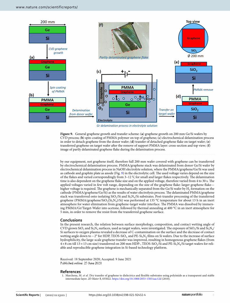
Prior to the deposition of graphene, 2 µm thick Ge(100) films were grown epitaxially on 200 mm Si(100) wafers28. Afterward, the monolayer graphene was grown on 200 mm Ge/Si wafers by CVD technique (Aixtron Black Magic BM300T CVD) at 885 °C temperature and 700 mbar pressure, using CH4 and Ar/H2 as a source and carrier gasses, respectively29. The poly(methyl methacrylate) (PMMA) polymer was spin-coated on top of the grown graphene to enable and support the graphene during the wet transfer procedure. For the spin coating the E-Beam Resist PMMA 950 K (Allresist) was used and coated with 4000 rpm rotation speed resulting in ca. 400 nm thickness of PMMA on the Gr/Ge/Si stacking.
The 200 mm wafers with PMMA/Gr/Ge/Si were cut into different pieces in the sizes from 4 × 8 cm till 13 × 13 cm before the delamination process. The size of transferred graphene flake of 13 × 13 cm is only limited
Figure 7. Schematic representation of possible surface modification after oxygen plasma and exposure to ambient.
Figure 8. Optical microscopy picture of (a) graphene flake transferred on HDP-SiO2 surface with wettability angle of 2.4°, (b) schematic drawing of water drop on the surface with WCA = 2.4°, (c) large-scale PMMA/graphene flake transferred on HDP-SiO2/Si surface (d) transferred graphene flakes (without PMMA resist) on structured 200 mm wafer.
8
Vol:.(1234567890)
Scientific Reports | (2021) 11:13111 | https://doi.org/10.1038/s41598-021-92432-4
www.nature.com/scientificreports/
by our equipment, not graphene itself, therefore full 200 mm wafer covered with graphene can be transferred by electrochemical delamination process. PMMA/graphene stack was delaminated from donor Ge/Si wafer by electrochemical delamination process in NaOH electrolyte solution, where the PMMA/graphene/Ge/Si was used as cathode and graphite plate as anode (Fig. 9) in the electrolytic cell. The used voltage varies depend on the size of the flakes and varied correspondingly from 3–12 V, for small and larger flakes respectively. The delamination time is also dependent on the graphene flake size and on the applied voltage, therefore varied from 4 to 30 s. The applied voltages varied in few volt range, depending on the size of the graphene flake: larger graphene flake—higher voltage is required. The graphene is mechanically separated from the Ge/Si wafer by H2 formation on the cathode (PMMA/graphene/Ge/Si) as the results of water electrolysis process. The delaminated PMMA/graphene stack was transferred onto isolating SiO2/Si and Si3N4/Si substrates. Post-transfer processing of the transferred graphene (PMMA/graphene/SiO2(Si3N4)/Si) was performed at 135 °C temperature for about 13 h in an inert atmosphere for water elimination from graphene-target wafer interface. The PMMA was dissolved by immers-ing PMMA/Gr/Target-Wafer into acetone, followed by thermal annealing at 400 °C in an inert atmosphere for 5 min, in order to remove the resist from the transferred graphene surface.
ConclusionsIn the present research, the relation between surface morphology, composition, and contact wetting angle of CVD grown SiO2 and Si3N4 surfaces, used as target wafers, were investigated. The exposure of SiO2/Si and Si3N4/Si surfaces to oxygen plasma revealed a decrease of C-contamination on the surface and the decrease of contact wetting angle down to ~ 2° for HDP, TEOS-SiO2, and PE-Si3N4 films on Si wafers. Due to the increase of surface hydrophilicity, the large-scale graphene transfer was improved, resulting in homogenous graphene flakes (from 4 × 8 cm till 13 × 13 cm size) transferred on 200 mm HDP-, TEOS-SiO2/Si and PE-Si3N4/Si target wafers for reli-able and reproducible graphene integration in Si-based technology platform.
Received: 18 September 2020; Accepted: 9 June 2021
References 1. Marchena, M. et al. Dry transfer of graphene to dielectrics and flexible substrates using polyimide as a transparent and stable
intermediate layer. 2D Mater 5, 035022. https:// doi. org/ 10. 1088/ 2053- 1583/ aac12d (2018).
Figure 9. General graphene growth and transfer scheme: (a) graphene growth on 200 mm Ge/Si wafers by CVD process; (b) spin-coating of PMMA polymer on top of graphene; (c) electrochemical delamination process in order to detach graphene from the donor wafer; (d) transfer of detached graphene flake on target wafer; (e) transferred graphene on target wafer after the remove of support PMMA layer: cross-section and top view; (f) image of partly delaminated graphene flake during the delamination process.
9
Vol.:(0123456789)
Scientific Reports | (2021) 11:13111 | https://doi.org/10.1038/s41598-021-92432-4
www.nature.com/scientificreports/
2. Bae, S. et al. Roll-to-roll production of 30-inch graphene films for transparent electrodes. Nat. Nanotechnol 5, 574–578. https:// doi. org/ 10. 1038/ nnano. 2010. 132 (2010).
3. Kang, J. et al. Efficient transfer of large-area graphene films onto rigid substrates by hot pressing. ACS Nano 6, 5360–5365. https:// doi. org/ 10. 1021/ nn301 207d (2012).
4. Caldwell, J. D. et al. Technique for the dry transfer of epitaxial graphene onto arbitrary substrates. ACS Nano 4, 1108–1114. https:// doi. org/ 10. 1021/ nn901 585p (2010).
5. Lock, E. H. et al. High-quality uniform dry transfer of graphene to polymers. Nano Lett 12, 102–107. https:// doi. org/ 10. 1021/ nl203 058s (2012).
6. Jung, S. et al. Reduction of water-molucule-induced current-voltage hysteresis in graphene field effect transistor with semi-dry transfer using flexible supporter. J. Appl. Phys. 125, 184302. https:// doi. org/ 10. 1063/1. 50894 94 (2019).
7. Mattevi, C., Kim, H. & Chhowalla, M. A review of chemical vapour deposition of graphene on copper. J. Mater. Chem 21, 3324–3334. https:// doi. org/ 10. 1039/ C0JM0 2126A (2011).
8. Wang, Y. et al. Electrochemical delamination of CVD-grown graphene film: toward the recyclable use of copper catalyst. ACS Nano 5, 9927–9933. https:// doi. org/ 10. 1021/ nn203 700w (2011).
9. Gupta, P. et al. A facile process for soak-and-peel delamination of CVD graphene from substrates using water. Sci. Rep 4, 3882. https:// doi. org/ 10. 1038/ srep0 3882 (2015).
10. Seo, J. et al. Direct graphene transfer and its application to transfer printing using mechanically controlled, large area graphene/copper freestanding layer. Adv. Funct. Mater 28, 1707102. https:// doi. org/ 10. 1002/ adfm. 20170 7102 (2018).
11. Bae, S. et al. Roll-to-roll production of 30-inch graphene films for transparent electrodes, Nat. Nanotechnol 5, 574–578. http:// www. nature. com/ doifi nder/, https:// doi. org/ 10. 1038/ nnano. 2010. 132 (2010).
12. Verguts, K. Controling water intercalation is key to a direct graphene transfer. ACS Appl. Mater. Interfaces 9, 37484–37492. https:// doi. org/ 10. 1021/ acsami. 7b125 73 (2017).
13. Ma, D. et al. Clean transfer of graphene on Pt foils mediated by a carbon monoxide intercalation process. Nano Res 6, 671–678. https:// doi. org/ 10. 1007/ s12274- 013- 0342-6 (2013).
14. Ohtomo, M., Sekine, Y., Wang, S., Hibino, H. & Yamamoto, H. Etchant-free graphene transfer using facile intercalation of alka-nethiol self-assembled molecules at graphene/metal interfaces. Nanoscale 8, 11503–11510. https:// doi. org/ 10. 1039/ C6NR0 1366J (2016).
15. Lupina, G. et al. Residual metallic contamination of transferred chemical vapor deposited graphene. ACS Nano 9, 4776–4785. https:// doi. org/ 10. 1021/ acsna no. 5b012 61 (2015).
16. Sun, J. et al. Mechanism of electrochemical delamination of two-dimensional materials from their native substrates by bubbling. Sensors 15, 31811–31820. https:// doi. org/ 10. 3390/ s1512 29888 (2015).
17. Cherian, C. T. et al. ‘Bubble-free’ electrochemical delamination of CVD graphene films. Small 11, 189–194. https:// doi. org/ 10. 1002/ smll. 20140 2024 (2015).
18. Das, S., Lahiri, D., Agarwal, A. & Choi, W. Interfacial bonding characteristics between graphene and dielectric substrates. Nano-technol 25, 045707. https:// doi. org/ 10. 1088/ 0957- 4484/ 25/4/ 045707 (2014).
19. Kim, H. H., Lee, S. K., Lee, S. G., Lee, E. & Cho, K. Wetting-assisted crack- and wrinkle-free transfer of wafer-scale graphene onto arbitrary substrates over a wide range of surface energies. Adv. Funct. Mater 26, 2070–2077. https:// doi. org/ 10. 1002/ adfm. 20150 4551 (2016).
20. Knapp, M., Hoffmann, R., Cimalla, V. & Ambacher, O. Wettability investigations and wet transfer enhancement of large-area CVD-graphene on aluminum nitride. Nanomater 7, 226. https:// doi. org/ 10. 3390/ nano7 080226 (2017).
21. Williams, D. L. et al. Computerised measurement of contact angles. Galvanotechnik 101, 2502–2512 (2010). 22. Quere, D. Wetting and roughness. Annu. Rev. Mater. Sci 38, 71–99. https:// doi. org/ 10. 1146/ annur ev. matsci. 38. 060407. 132434
(2008). 23. Zhang, F., Kibria, M. G., Cormier, K. & Howlader, M. Surface and interface characterization of sequentially plasma activated
silicon, silicon dioxide and germanium wafers for low temperature bonding applications. ECS Trans 33, 329. https:// doi. org/ 10. 1149/1. 34835 22 (2010).
24. Luhmann, N. et al. Effect of oxygen plasma on nanomechanical silicon nitride resonators. Appl. Phys. Lett 111, 063103. https:// doi. org/ 10. 1063/1. 49897 75 (2017).
25. Lee, J. H. et al. Characteristic of SiO2 films deposited by using low-temperature PECVD with TEOS/N2/O2. J. Korean Phys. Soc 46, 890–894 (2005).
26. Yang, G.-R., Zhao, Y. P., Hu, Y. Z., Chow, T. P. & Gutmann, R. J. XPS and AFM study of chemical mechanical polishing of silicon nitride. Thin Solid Films 333, 219–223. https:// doi. org/ 10. 1016/ S0040- 6090(98) 00818-9 (1998).
27. Se, K., Kim, M., Kim, D. H. Re-derivation of Young’s Equation, Wenzel Equation, and Cassie-Baxter Equation Based on Energy Minimization. In: M. Aliofkhazraei, Surface Energy, IntechOpen, https:// doi. org/ 10. 5772/ 61066 (2015).
28. Yamamoto, Y., Zaumseil, P., Arguirov, T., Kittler, M. & Tillack, B. Low threading dislocation density Ge deposited on Si(100) using RPCVD. Solid State Electron 60, 2–6. https:// doi. org/ 10. 1016/j. sse. 2011. 01. 032 (2011).
29. Lukosius, M. et al. Metal-free CVD graphene synthesis on 200 mm Ge/Si (100) substrates. ACS Appl. Mat. Interfaces 8(49), 33786–33793. https:// doi. org/ 10. 1021/ acsami. 6b113 97 (2016).
AcknowledgementsThe authors are thankful for U. Saarow and P. Heinrich for AFM measurements and evaluation. This research was funded by: (1) the Federal Ministry of Education and Research (BMBF) Germany under grant GIMMIK No 03XP0210E; (2) the European Union’s Horizon 2020 research and innovation programme under Graphene Flagship grant agreement No 952792. (3) on the basis of the Ministry’s policy for science, research and culture (MWFK) to promote the “strengthening of technological and application-oriented research at scientific institu-tions in the state of Brandenburg "(StaF-Guideline) of March 6, 2015 in the version of January 24, 2019 and §§ 23 and 44 of the state budget regulations of the state of Brandenburg and the associated administrative regulations (Grant GETiT No 85038097). This funding is co-financed with funds from the European Regional Development Fund (ERDF).
Author contributionsM.L. performed 8 graphene growth experiments. R.L. performed graphene transfer and WCA measurements. M.Li., T.G. planned and performed SiO2 and Si3N4 depositions on 8 wafers. F.A. performed XPS and Raman measurements. M.F. performed plasma etching experiments. R.L, M.L., M.Li., A.M. analysed the experimental results. All authors reviewed the manuscript.
10
Vol:.(1234567890)
Scientific Reports | (2021) 11:13111 | https://doi.org/10.1038/s41598-021-92432-4
www.nature.com/scientificreports/
FundingOpen Access funding enabled and organized by Projekt DEAL.
Competing interests The authors declare no competing interests.
Additional informationSupplementary Information The online version contains supplementary material available at https:// doi. org/ 10. 1038/ s41598- 021- 92432-4.
Correspondence and requests for materials should be addressed to R.L.
Reprints and permissions information is available at www.nature.com/reprints.
Publisher’s note Springer Nature remains neutral with regard to jurisdictional claims in published maps and institutional affiliations.
Open Access This article is licensed under a Creative Commons Attribution 4.0 International License, which permits use, sharing, adaptation, distribution and reproduction in any medium or
format, as long as you give appropriate credit to the original author(s) and the source, provide a link to the Creative Commons licence, and indicate if changes were made. The images or other third party material in this article are included in the article’s Creative Commons licence, unless indicated otherwise in a credit line to the material. If material is not included in the article’s Creative Commons licence and your intended use is not permitted by statutory regulation or exceeds the permitted use, you will need to obtain permission directly from the copyright holder. To view a copy of this licence, visit http:// creat iveco mmons. org/ licen ses/ by/4. 0/.
© The Author(s) 2021