initial tests of a compact imaging photomultiplier made ... · initial tests of a compact imaging...
TRANSCRIPT

Initial Tests of a Compact Imaging Photomultiplier
Made From Array of 3x3mm2 Hamamatsu MPPC-
SMD Modules
S. Majewski1, J. Proffitt1, J. McKisson1, R.Raylman2, A. Stolin1 and A.G. Weisenberger1
1Radiation Detector & Medical Imaging Group, Thomas Jefferson National Accelerator Facility, Newport News, VA
2Center for Advanced Imaging, Department of Radiology, West Virginia University, Morgantown, WV
Abstract– We built and tested the first small (~18mm square)
prototype compact photomultiplier (PM) consisting of a 4x4
array of individual 3x3mm2 Hamamatsu Multi-Pixel Photon
Counters (MPPC). To reduce the cost and complexity, the
3x3mm2 units were not arranged in the tightest possible
arrangement, but spaced at 5mm (center-to-center). The MPPC-
PM package includes low power on-board input stage amplifiers
for each MPPC element and a sum amplifier placed on additional
distant electronics board. The initial studies were performed with
arrays of LYSO, NaI(Tl) and CsI(Tl) irradiated with Co57
and
Na22
sources. The PM performed best when used with LYSO
arrays exposed to annihilation photons, indicating good prospects
for use in PET applications. Tests in 3 Tesla MRI magnet showed
no detectable impact on operation of the PM. The expected and
confirmed drawback of this device is that SiPM gain is quite
sensitive to temperature (gain decreases with rising temperature),
and maintaining temperature stability will present the main
practical challenge in using this new PM. During the tests the
constantly monitored temperature of the PM was between 28-30
deg C. Rate performance, another potential issue with this device,
was not studied at this time. We are now constructing and
planning next devices with more compact electronics packages
and with larger fields of view. The ultimate goal of the project is
to utilize the MPPC-PM modules as building blocks of larger
devices, with active arrays as large as 5x5cm2 and beyond.
I. INTRODUCTION
Silicon Photomultipliers (SiPMs) are a new type of photon
counting device made up of multiple avalanche photodiodes
(APD) pixels operated in Geiger mode. They have much
higher gain (105-106) than standard APDs. Thus, these devices
could potentially replace standard photomultipliers in a
number of applications. For example, the nuclear physics
program at Jefferson Lab is considering use of SiPMs in
calorimetric detectors placed in tight places of the detection
system apparatus, and in strong (several Tesla) magnetic
fields. The present investigation started as a spin-off of that
development.
After the initial Russian–based development effort [1],
many R&D projects around the world are focusing on the
development and application of SiPMs to biomedical imaging;
initially for small size imagers applicable to small animal
imaging, but also for dedicated human imagers. The number of
technical efforts around the world focusing on development of
different designs of SiPMs, and studies of their properties, as
well as on designing practical imagers, is increasing
dramatically within the last two years, with only few very
recent works referenced here [2-11].
The advantages of SiPMs are their very small size, and
ability to operate in strong magnetic fields. Thus, permitting
their use in multimodality (PET/MRI, SPECT/MRI) imagers,
supplanting the use of APDs in this application [10,11]. One
of the challenges in applying SiPMs to imaging is their small
size. Most individual units range in size from 1x1mm2 to
3x3mm2. In addition, these devices do not have the capability
to provide positional information (as position sensitive
photomultipliers (PSPMTs) do). It is therefore necessary to
produce arrays of the devices to create a unit appropriate for
imaging application. In other words, each SiPMs operates as
an individual anode pad present on PSPMTs.
There are currently a number of companies developing
SiPMs. SensL Corp. [12], Hamamatsu Photonics [13], three
original entities in Russia [14-16], Radiation Monitoring
Devices [17], Zecotek [18], Photonique [19] and other newly
formed companies, as well as an Italian consortium [20] are all
developing SiPMs, under different names. At this time, we are
working with two suppliers of silicon SiPMs: SensL and
Hamamatsu. We acquired samples of SiPM from both
companies. Currently, SensL is more advanced in the
development of small-integrated imaging arrays than
Hamamatsu.
Typically SiPM modules come in small units of 1mm2-
3mm2 in size. Therefore, arrays of these devices are needed to
cover the desired active field of view. Figure 1 shows an
example of how to achieve a SiPM photodetector of up to
~5x5cm2 active field of view using hypothetical ~12.5mm
modules composed of tightly spaced 3x3mm2 SiPM units. For
example, the initial imaging module can be composed of an
array of sixteen 3x3mm2 readout pixels/pads arranged in a 4x4
array. These imaging modules should be four-sides buttable
with a dead space on the order of 1mm or less at the edges. By
assembling them in an array, these basic modules can be
arranged to form larger size imaging macro-modules, for
example composed of 4x4 basic modules, with coverage and
readout needs equivalent to the H8500/9500 flat panel PSPMT
(Figure 1). The 3x3mm2 pads can be either read separately or
coarsely with four or all 16 pads connected to one readout
channel, as shown schematically at left center and bottom of
Figure 1, respectively. In this design, an array of 2x2 of these
basic four-sides buttable modules (8x8=64 of 3x3mm2 pads)
forms a ~1” square photodetector, equivalent for example to

Hamamatsu R8520-C12 PSPMT. Next, the concept for a
“plug-in” replacement module for the H8500/H9500 flat PMT
with about ~5x5cm2 active surface can be implemented.
Currently, some of the SiPM devices are not yet
sufficiently sensitive in the blue spectral region of the LaBr3
emission. For example, the sensitivity of devices from SensL
peaks at 520 nm, with poor response at 400nm. In contrast, the
spectral response of Hamamatsu devices has a good match
with the emission of LaBr3 (Figure 2). As many applications
of SiPMs depend in a crucial way on this extension of the
SiPM sensitivity, therefore it is anticipated that similar SiPM
designs from SensL and from other companies will be
available in the near future.
Figure 1. Concept of building larger photodetector modules from
~3x3mm2 SiPM units. One example of the basic module, shown
schematically at left top, is composed of an array of 4x4 3x3mm2
active pads. These basic modules can be read as 16, 4, or 1
individual channels. They can be in turn arranged in arrays to
form SiPM equivalents of PSPMT structures such as Hamamatsu
R8520 (center) and H9500 (at right).
Figure 2. Spectral response efficiency of several designs of
Hamamatsu MPPCs (SiPMs). The last number (before U) denotes
size of the basic Geiger microcell (25, 50 or 100 micron). Please
note good match with LaBr3 emission (Hamamatsu data).
II. MPPC MODULES
Hamamatsu Photonics [13] introduced very recently their
3x3mm2 silicon PM, called MPPC, in a more compact SMD
package (Figure 3). It is possible that tight arrays of these
sensors can now be assembled resulting in a detector with a
large sensor area. Conceivably good quality imaging could be
achieved through the readout on individual 3x3mm2 sensor
elements butted together on a ~4.3 (x) by 4.8 mm (y) pitch.
This could be possible with the use of an optical light guide
window as long as sufficient sampling of the scintillation
signal is possible to obtain strong enough detection signal and
if good light sharing occurs.
Figure 3. Schematic drawing of the new 3x3mm2-MPPC-SMD
SiPM package from Hamamatsu (model S10362-33-050SMD).
(Drawing provided by Hamamatsu Photonics).
III. PM PACKAGE
As mentioned above, useful FOV devices can be obtained
by assembling arrays of smaller basic SiPM modules, such as
the 3x3mm2 MPPC unit from Hamamatsu. A high level of
flexibility of size choices is now available to users, with the
complication of required special design for each device.
However, development of several sizes of basic building
blocks can facilitate this task (Figure 1).
Imaging with SiPM arrays was so far demonstrated in very
small size devices [9], and usually with bulky test board type
electronics, not matching the size of the tested small
photodetector. Our approach was to attempt assembly of a PM
structure built from an array of “large” size (3mmx3mm)
SiPM modules, with compact matching size electronics
occupying space behind the photodetector. In this way, many
modules of this design can be assembled side by side to form a
larger device, as conceptually shown in Figure 1. We have
spaced the 3x3mm2 elements (model S10362-33-050SMD
with 50 micron microcell size) in a 4x4 array with a 5mm
pitch, to cover a larger surface with the same number of
3x3mm2 modules. Figures 4-6 show the construction of the
PM and the photograph in Figure 7 indicates how we
constructed the first small detector module using a matching
size scintillation array. As in our past work with arrays of
PSPMTs, we implemented a light guide “spreader” window to
allow for scintillation light to spread between neighboring
3x3mm2 active elements for proper operation of the center of
gravity algorithm for scintillation arrays with pixel pitch
smaller than the PM active pad pitch (5mm in this case).
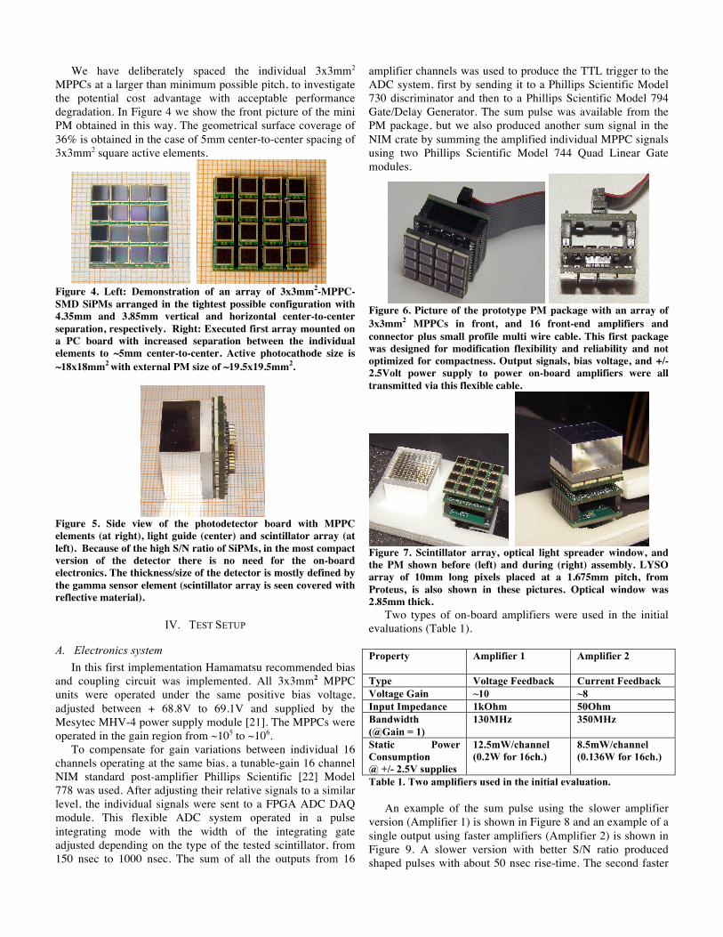
We have deliberately spaced the individual 3x3mm2
MPPCs at a larger than minimum possible pitch, to investigate
the potential cost advantage with acceptable performance
degradation. In Figure 4 we show the front picture of the mini
PM obtained in this way. The geometrical surface coverage of
36% is obtained in the case of 5mm center-to-center spacing of
3x3mm2 square active elements.
Figure 4. Left: Demonstration of an array of 3x3mm
2-MPPC-
SMD SiPMs arranged in the tightest possible configuration with
4.35mm and 3.85mm vertical and horizontal center-to-center
separation, respectively. Right: Executed first array mounted on
a PC board with increased separation between the individual
elements to ~5mm center-to-center. Active photocathode size is
~18x18mm2
with external PM size of ~19.5x19.5mm2.
Figure 5. Side view of the photodetector board with MPPC
elements (at right), light guide (center) and scintillator array (at
left). Because of the high S/N ratio of SiPMs, in the most compact
version of the detector there is no need for the on-board
electronics. The thickness/size of the detector is mostly defined by
the gamma sensor element (scintillator array is seen covered with
reflective material).
IV. TEST SETUP
A. Electronics system
In this first implementation Hamamatsu recommended bias
and coupling circuit was implemented. All 3x3mm2 MPPC
units were operated under the same positive bias voltage,
adjusted between + 68.8V to 69.1V and supplied by the
Mesytec MHV-4 power supply module [21]. The MPPCs were
operated in the gain region from ~105 to ~106.
To compensate for gain variations between individual 16
channels operating at the same bias, a tunable-gain 16 channel
NIM standard post-amplifier Phillips Scientific [22] Model
778 was used. After adjusting their relative signals to a similar
level, the individual signals were sent to a FPGA ADC DAQ
module. This flexible ADC system operated in a pulse
integrating mode with the width of the integrating gate
adjusted depending on the type of the tested scintillator, from
150 nsec to 1000 nsec. The sum of all the outputs from 16
amplifier channels was used to produce the TTL trigger to the
ADC system, first by sending it to a Phillips Scientific Model
730 discriminator and then to a Phillips Scientific Model 794
Gate/Delay Generator. The sum pulse was available from the
PM package, but we also produced another sum signal in the
NIM crate by summing the amplified individual MPPC signals
using two Phillips Scientific Model 744 Quad Linear Gate
modules.
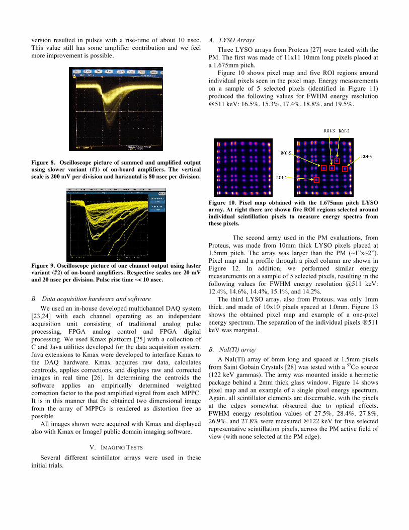
Figure 6. Picture of the prototype PM package with an array of
3x3mm2 MPPCs in front, and 16 front-end amplifiers and
connector plus small profile multi wire cable. This first package
was designed for modification flexibility and reliability and not
optimized for compactness. Output signals, bias voltage, and +/-
2.5Volt power supply to power on-board amplifiers were all
transmitted via this flexible cable.
Figure 7. Scintillator array, optical light spreader window, and
the PM shown before (left) and during (right) assembly. LYSO
array of 10mm long pixels placed at a 1.675mm pitch, from
Proteus, is also shown in these pictures. Optical window was
2.85mm thick.
Two types of on-board amplifiers were used in the initial
evaluations (Table 1).
Property Amplifier 1
Amplifier 2
Type Voltage Feedback Current Feedback
Voltage Gain ~10 ~8
Input Impedance 1kOhm 50Ohm
Bandwidth
(@Gain = 1)
130MHz 350MHz
Static Power
Consumption
@ +/- 2.5V supplies
12.5mW/channel
(0.2W for 16ch.)
8.5mW/channel
(0.136W for 16ch.)
Table 1. Two amplifiers used in the initial evaluation.
An example of the sum pulse using the slower amplifier
version (Amplifier 1) is shown in Figure 8 and an example of a
single output using faster amplifiers (Amplifier 2) is shown in
Figure 9. A slower version with better S/N ratio produced
shaped pulses with about 50 nsec rise-time. The second faster
version resulted in pulses with a rise-time of about 10 nsec.
This value still has some amplifier contribution and we feel
more improvement is possible.
Figure 8. Oscilloscope picture of summed and amplified output
using slower variant (#1) of on-board amplifiers. The vertical
scale is 200 mV per division and horizontal is 80 nsec per division.
Figure 9. Oscilloscope picture of one channel output using faster
variant (#2) of on-board amplifiers. Respective scales are 20 mV
and 20 nsec per division. Pulse rise time ~< 10 nsec.
B. Data acquisition hardware and software
We used an in-house developed multichannel DAQ system
[23,24] with each channel operating as an independent
acquisition unit consisting of traditional analog pulse
processing, FPGA analog control and FPGA digital
processing. We used Kmax platform [25] with a collection of
C and Java utilities developed for the data acquisition system.
Java extensions to Kmax were developed to interface Kmax to
the DAQ hardware. Kmax acquires raw data, calculates
centroids, applies corrections, and displays raw and corrected
images in real time [26]. In determining the centroids the
software applies an empirically determined weighted
correction factor to the post amplified signal from each MPPC.
It is in this manner that the obtained two dimensional image
from the array of MPPCs is rendered as distortion free as
possible.
All images shown were acquired with Kmax and displayed
also with Kmax or ImageJ public domain imaging software.
V. IMAGING TESTS
Several different scintillator arrays were used in these
initial trials.
A. LYSO Arrays
Three LYSO arrays from Proteus [27] were tested with the
PM. The first was made of 11x11 10mm long pixels placed at
a 1.675mm pitch.
Figure 10 shows pixel map and five ROI regions around
individual pixels seen in the pixel map. Energy measurements
on a sample of 5 selected pixels (identified in Figure 11)
produced the following values for FWHM energy resolution
@511 keV: 16.5%, 15.3%, 17.4%, 18.8%, and 19.5%.
Figure 10. Pixel map obtained with the 1.675mm pitch LYSO
array. At right there are shown five ROI regions selected around
individual scintillation pixels to measure energy spectra from
these pixels.
The second array used in the PM evaluations, from
Proteus, was made from 10mm thick LYSO pixels placed at
1.5mm pitch. The array was larger than the PM (~1”x~2”).
Pixel map and a profile through a pixel column are shown in
Figure 12. In addition, we performed similar energy
measurements on a sample of 5 selected pixels, resulting in the
following values for FWHM energy resolution @511 keV:
12.4%, 14.6%, 14.4%, 15.1%, and 14.2%.
The third LYSO array, also from Proteus, was only 1mm
thick, and made of 10x10 pixels spaced at 1.0mm. Figure 13
shows the obtained pixel map and example of a one-pixel
energy spectrum. The separation of the individual pixels @511
keV was marginal.
B. NaI(Tl) array
A NaI(Tl) array of 6mm long and spaced at 1.5mm pixels
from Saint Gobain Crystals [28] was tested with a 57Co source
(122 keV gammas). The array was mounted inside a hermetic
package behind a 2mm thick glass window. Figure 14 shows
pixel map and an example of a single pixel energy spectrum.
Again, all scintillator elements are discernable, with the pixels
at the edges somewhat obscured due to optical effects.
FWHM energy resolution values of 27.5%, 28.4%, 27.8%,
26.9%, and 27.8% were measured @122 keV for five selected
representative scintillation pixels, across the PM active field of
view (with none selected at the PM edge).
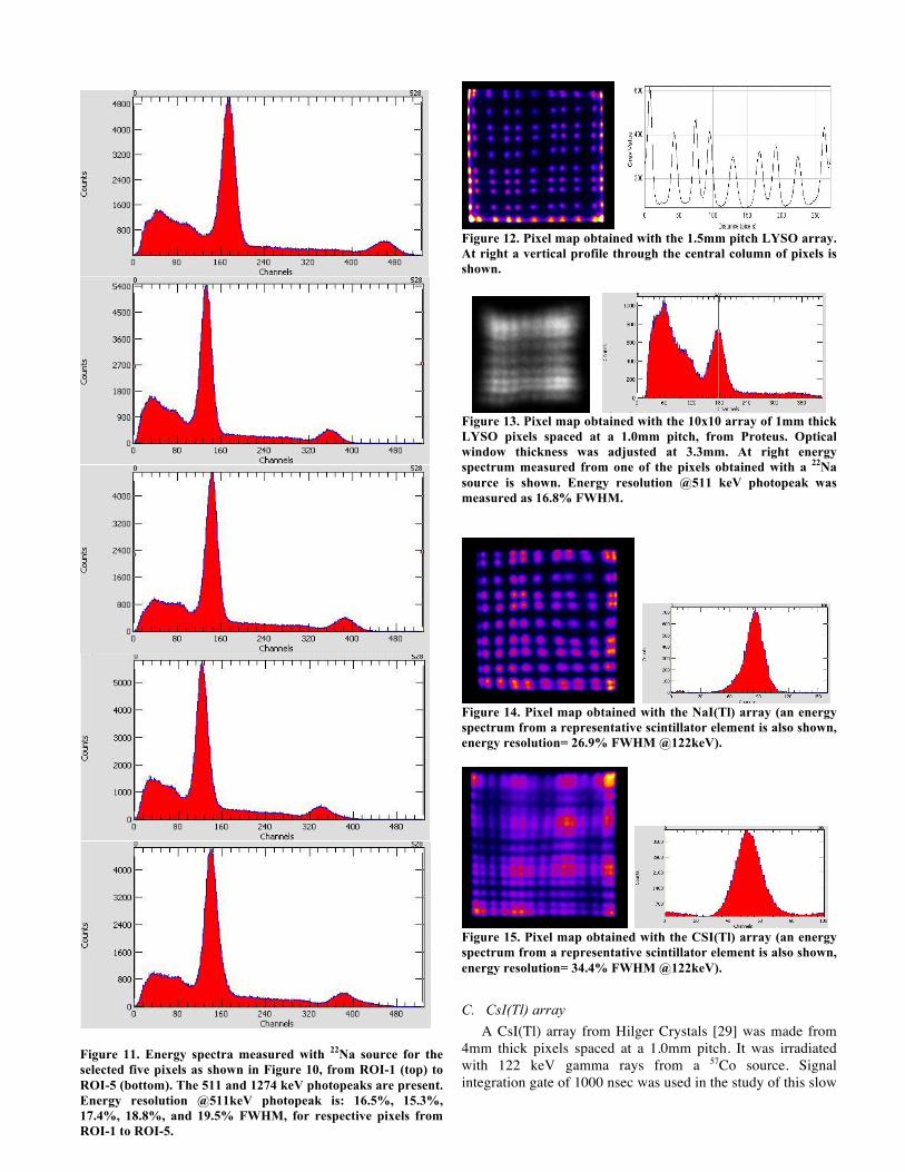
Figure 12. Pixel map obtained with the 1.5mm pitch LYSO array.
At right a vertical profile through the central column of pixels is
shown.
Figure 13. Pixel map obtained with the 10x10 array of 1mm thick
LYSO pixels spaced at a 1.0mm pitch, from Proteus. Optical
window thickness was adjusted at 3.3mm. At right energy
spectrum measured from one of the pixels obtained with a 22
Na
source is shown. Energy resolution @511 keV photopeak was
measured as 16.8% FWHM.
Figure 14. Pixel map obtained with the NaI(Tl) array (an energy
spectrum from a representative scintillator element is also shown,
energy resolution= 26.9% FWHM @122keV).
Figure 15. Pixel map obtained with the CSI(Tl) array (an energy
spectrum from a representative scintillator element is also shown,
energy resolution= 34.4% FWHM @122keV).
C. CsI(Tl) array
A CsI(Tl) array from Hilger Crystals [29] was made from
4mm thick pixels spaced at a 1.0mm pitch. It was irradiated
with 122 keV gamma rays from a 57Co source. Signal
integration gate of 1000 nsec was used in the study of this slow
Figure 11. Energy spectra measured with
22Na source for the
selected five pixels as shown in Figure 10, from ROI-1 (top) to
ROI-5 (bottom). The 511 and 1274 keV photopeaks are present.
Energy resolution @511keV photopeak is: 16.5%, 15.3%,
17.4%, 18.8%, and 19.5% FWHM, for respective pixels from
ROI-1 to ROI-5.
scintillator. A 2.85mm thick acrylic spreader window was
placed between the array and the PM. Figure 15 shows pixel
maps and example of a single pixel energy spectrum from this
array. FWHM energy resolution values of 32.0%, 32.7%,
34.4%, 33.8%, and 32.8% were measured @122 keV for
similarly selected 5 representative scintillation pixels, across
the PM active field of view (none was selected at the PM
edge). The pixel separation in some regions of the PM was
marginal at this initial test. The effect of scintillation light cone
signal under-sampling is evident from the non-uniform pixel
distribution in the pixel map. A very similar effect was
observed with the 1mm LYSO array (Figure 13). In the next
planned series of measurements the optical coupling will be re-
optimized. Specifically, we will investigate wet optical
coupling as opposed to dry coupling used throughout these
initial studies.
The results of the above initial studies with three of the
most common scintillators in Nuclear Medicine Imaging:
LYSO, NaI(Tl) and CsI(Tl), confirm that with added light
guide (spreader) window, the 5mm granularity of the
constructed PM structure is adequate to efficiently sample
scintillation light to achieve high response uniformity and
pixel separation, but for pixel pitches larger than 1mm.
D. Optical coupling studies
After the first series of measurements with different
scintillator arrays with no special measures to increase light
collection, we performed a short pilot study to re-optimize
collection of scintillation light the by the active PM elements.
To this effect we placed a net of 2mm wide reflector strips
made of white Millipore paper. Also, different edge treatments
of the window light spreader were tested with no treatment
(rough cut), polished, and white and black paint finish.
At this time, our optimized design has Millipore reflectors
and rough-cut UV acrylic window edges. Further studies are
planned. In addition to improved response uniformity across
the PM surface, and better energy resolution, a much improved
visibility of the outer pixels was obtained.
Figure 16. Left: Pixel map of 11x11 LYSO pixel array of
1.675mm pixels @511 keV using improved optical coupling with
Millipore reflectors. Right: detail of the left upper corner region
with four selected corner pixels. Energy resolution over selected
ROI regions was between 13.0% and 13.9%. Signal amplitude
from the very edge pixel was lowest in the detector and lower by
~35% compared to central pixels. Corner pixels exhibited
following FWHM energy resolution @511 keV: 19.4% (the very
corner pixel), 17.0% (right top corner pixel) , 16.9% (left lower
corner pixel), 19.4% (inner corner pixel).
Figure 16 shows the improved pixel map of the 1.675mm
LYSO array (to be compared with Figure 10). Energy
resolution in the major part of the PM surface improved to
~13.5% FWHM @511 keV, while the corner pixels (the worst
case scenario) had energy resolution between 17.0 and 19.4%.
VI. TESTS IN MRI FIELD
A. MPPC studies in MRI magnet
We have first tested two individual 3x3mm2 MPPC units
mounted at 90 degrees to each other on a test board with
amplifiers (Figure 17). Two units were used to investigate
simultaneously if field direction affected operation of the
MPPC device, with one set of measurements having the face
of the first module perpendicular to the magnetic flux lines and
one set with the flux lines parallel to the second module’s face.
These were 3x3mm2 Hamamatsu S10362-33-050C MPPCs, in
different packaging but with the similar structure to the model
used to construct our imaging PM. The effects of a magnetic
field on the operation of the MPPC were assessed by placing
the board with two MPPCs in magnetic fields with strength of
0, 0.5, 1.0, 1.5, 2.0 and 3.0T.
The studies were done at the West Virginia University’s
Health Sciences Center. Specifically, the unit was placed at
various distances from the isocenter of a 3T MRI system (GE
Medical Systems, Inc.). The magnetic field strength was
monitored with a three-axis Hall probe. At each magnetic
field strength, data were acquired from the module while it
was irradiated with a 40µCi 18F source.
Figure 17. Test board with two orthogonally mounted MPPCs
dry-coupled to 3x3x10mm GSO crystals, seen wrapped with white
Teflon tape. The board was inserted into magnet bore with its
horizontal (left to right) axis aligned with the magnet bore axis.
The second sensor was orthogonal to the magnetic field
throughout the tests.
No effects from the magnetic field were noticed on the
performance of the two sensors (including the input stage
amplifiers). Both MPPC outputs were nearly identical and
constant as the field was changed. The small amplitude
variations shown in Figure 18 were associated with
temperature variations of the sensors and board. The
measurements were not performed in the order of rising field,
but from low value of 0.4 Tesla went to 2 Tesla and 3 Tesla,
and then to intermediate values of 1.5 and 1.0 Tesla, and this
explains why the peak amplitude seen in the plot is not
smoothly changing with the magnetic field value.
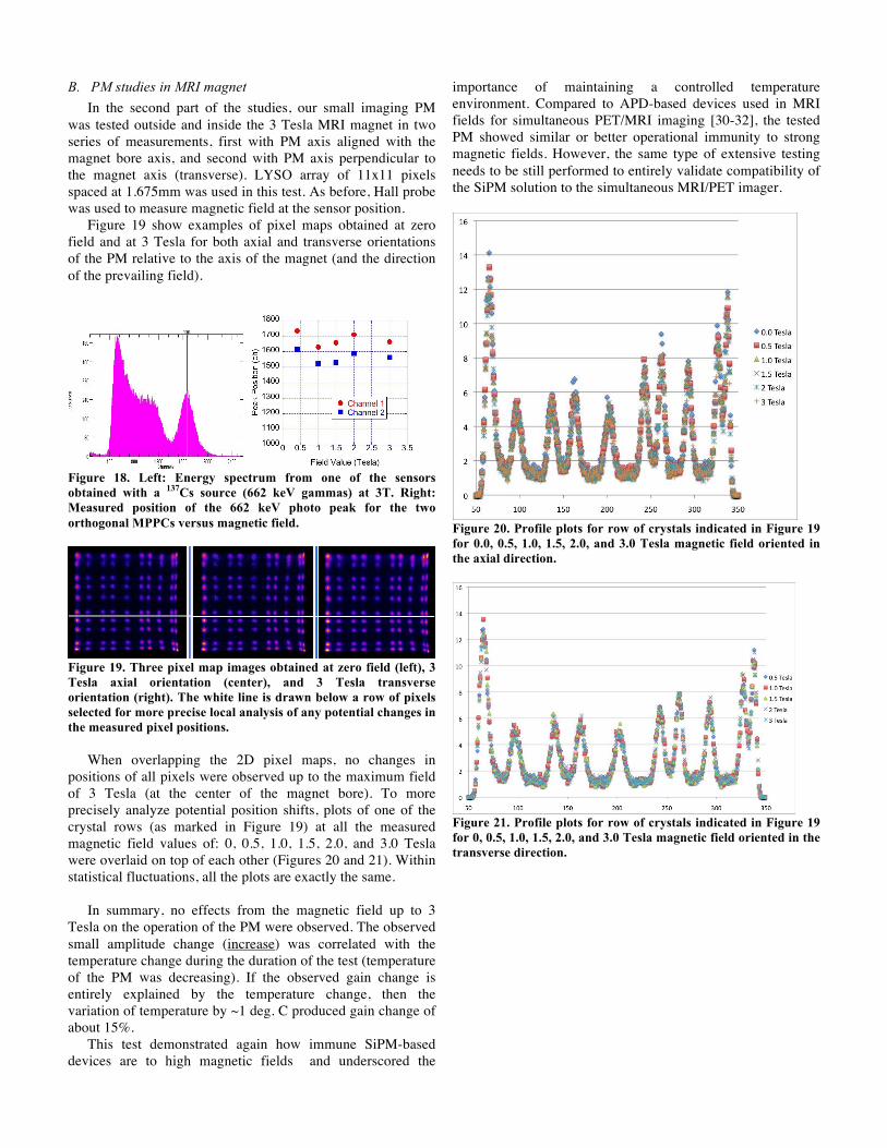
B. PM studies in MRI magnet
In the second part of the studies, our small imaging PM
was tested outside and inside the 3 Tesla MRI magnet in two
series of measurements, first with PM axis aligned with the
magnet bore axis, and second with PM axis perpendicular to
the magnet axis (transverse). LYSO array of 11x11 pixels
spaced at 1.675mm was used in this test. As before, Hall probe
was used to measure magnetic field at the sensor position.
Figure 19 show examples of pixel maps obtained at zero
field and at 3 Tesla for both axial and transverse orientations
of the PM relative to the axis of the magnet (and the direction
of the prevailing field).
Figure 18. Left: Energy spectrum from one of the sensors
obtained with a 137
Cs source (662 keV gammas) at 3T. Right:
Measured position of the 662 keV photo peak for the two
orthogonal MPPCs versus magnetic field.
Figure 19. Three pixel map images obtained at zero field (left), 3
Tesla axial orientation (center), and 3 Tesla transverse
orientation (right). The white line is drawn below a row of pixels
selected for more precise local analysis of any potential changes in
the measured pixel positions.
When overlapping the 2D pixel maps, no changes in
positions of all pixels were observed up to the maximum field
of 3 Tesla (at the center of the magnet bore). To more
precisely analyze potential position shifts, plots of one of the
crystal rows (as marked in Figure 19) at all the measured
magnetic field values of: 0, 0.5, 1.0, 1.5, 2.0, and 3.0 Tesla
were overlaid on top of each other (Figures 20 and 21). Within
statistical fluctuations, all the plots are exactly the same.
In summary, no effects from the magnetic field up to 3
Tesla on the operation of the PM were observed. The observed
small amplitude change (increase) was correlated with the
temperature change during the duration of the test (temperature
of the PM was decreasing). If the observed gain change is
entirely explained by the temperature change, then the
variation of temperature by ~1 deg. C produced gain change of
about 15%.
This test demonstrated again how immune SiPM-based
devices are to high magnetic fields and underscored the
importance of maintaining a controlled temperature
environment. Compared to APD-based devices used in MRI
fields for simultaneous PET/MRI imaging [30-32], the tested
PM showed similar or better operational immunity to strong
magnetic fields. However, the same type of extensive testing
needs to be still performed to entirely validate compatibility of
the SiPM solution to the simultaneous MRI/PET imager.
Figure 20. Profile plots for row of crystals indicated in Figure 19
for 0.0, 0.5, 1.0, 1.5, 2.0, and 3.0 Tesla magnetic field oriented in
the axial direction.
Figure 21. Profile plots for row of crystals indicated in Figure 19
for 0, 0.5, 1.0, 1.5, 2.0, and 3.0 Tesla magnetic field oriented in the
transverse direction.
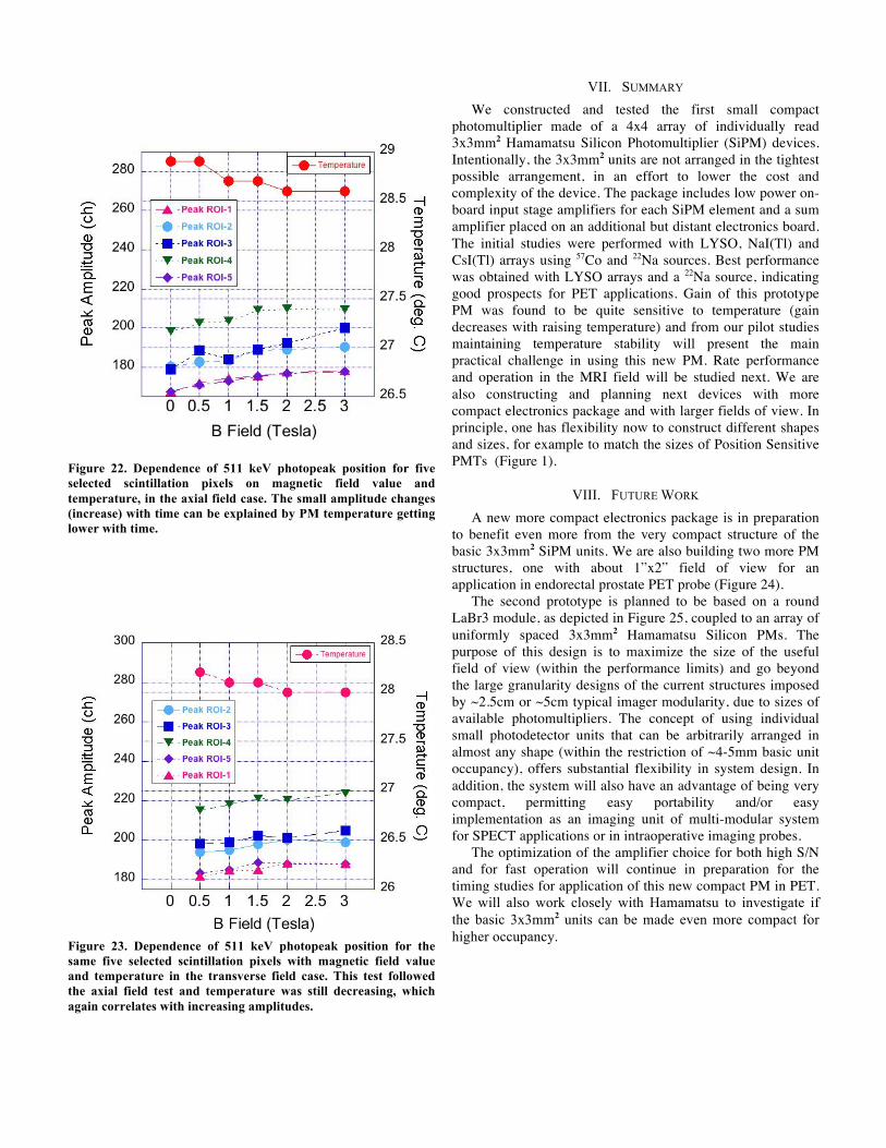
Figure 22. Dependence of 511 keV photopeak position for five
selected scintillation pixels on magnetic field value and
temperature, in the axial field case. The small amplitude changes
(increase) with time can be explained by PM temperature getting
lower with time.
Figure 23. Dependence of 511 keV photopeak position for the
same five selected scintillation pixels with magnetic field value
and temperature in the transverse field case. This test followed
the axial field test and temperature was still decreasing, which
again correlates with increasing amplitudes.
VII. SUMMARY
We constructed and tested the first small compact
photomultiplier made of a 4x4 array of individually read
3x3mm2 Hamamatsu Silicon Photomultiplier (SiPM) devices.
Intentionally, the 3x3mm2 units are not arranged in the tightest
possible arrangement, in an effort to lower the cost and
complexity of the device. The package includes low power on-
board input stage amplifiers for each SiPM element and a sum
amplifier placed on an additional but distant electronics board.
The initial studies were performed with LYSO, NaI(Tl) and
CsI(Tl) arrays using 57Co and 22Na sources. Best performance
was obtained with LYSO arrays and a 22Na source, indicating
good prospects for PET applications. Gain of this prototype
PM was found to be quite sensitive to temperature (gain
decreases with raising temperature) and from our pilot studies
maintaining temperature stability will present the main
practical challenge in using this new PM. Rate performance
and operation in the MRI field will be studied next. We are
also constructing and planning next devices with more
compact electronics package and with larger fields of view. In
principle, one has flexibility now to construct different shapes
and sizes, for example to match the sizes of Position Sensitive
PMTs (Figure 1).
VIII. FUTURE WORK
A new more compact electronics package is in preparation
to benefit even more from the very compact structure of the
basic 3x3mm2 SiPM units. We are also building two more PM
structures, one with about 1”x2” field of view for an
application in endorectal prostate PET probe (Figure 24).
The second prototype is planned to be based on a round
LaBr3 module, as depicted in Figure 25, coupled to an array of
uniformly spaced 3x3mm2 Hamamatsu Silicon PMs. The
purpose of this design is to maximize the size of the useful
field of view (within the performance limits) and go beyond
the large granularity designs of the current structures imposed
by ~2.5cm or ~5cm typical imager modularity, due to sizes of
available photomultipliers. The concept of using individual
small photodetector units that can be arbitrarily arranged in
almost any shape (within the restriction of ~4-5mm basic unit
occupancy), offers substantial flexibility in system design. In
addition, the system will also have an advantage of being very
compact, permitting easy portability and/or easy
implementation as an imaging unit of multi-modular system
for SPECT applications or in intraoperative imaging probes.
The optimization of the amplifier choice for both high S/N
and for fast operation will continue in preparation for the
timing studies for application of this new compact PM in PET.
We will also work closely with Hamamatsu to investigate if
the basic 3x3mm2 units can be made even more compact for
higher occupancy.

Figure 24. Example diagram of a small-size prostate PET probe
prototype detector module using the 3x3mm2 detection elements
shown in Figure 3, each assumed to occupy up to~5mm square in
size. In this example an active field of view of over 2.5cm (wide)
by 5cm (high) is covered. The readout of the scintillation array is
obtained by coupling the scintillation array to the photodetector
array via light spreader optical window.
Figure 25. Concept of the Prototype Module #2. Left: Design of
the proposed 6cm diameter 6mm thick LaBr3 scintillator module
from Saint Gobain. Right: Preliminary arrangement of 120 units
of 3x3mm2 SiPM modules from Hamamatsu, covering the 6cm
active diameter LaBr3 detector module shown at left.
IX. ACKNOWLEDGEMENTS
The Jefferson Science Associates (JSA) operates the
Thomas Jefferson National Accelerator Facility for the United
States Department of Energy under contract DE-AC05-
06OR23177. Support for this research came in part from the
DOE Office of Biological and Environmental Research and
from the DOE Office of Nuclear Physics. State of Virginia
provided key funds for the project via internal grant from
Jefferson Science Associates. This work was also supported in
part by the National Cancer Institute (Grant Number R01
CA094196). The authors acknowledge timely assistance of
Hamamatsu Photonics (Tom Bailey and Earl Hergert) in
providing the 3x3mm2 MPPC modules. We also thank Philip
Parkhurst from Proteus for promptly providing us the many
scintillator samples used in this pilot study.
X. REFERENCES
[1] B. Dolgoshein et al., “Status report on silicon photomultiplier
development and its applications”, Nuclear Instruments and
Methods in Physics Research A 563 (2006) 368–376.
[2] G. Llosa et al, “Novel Silicon Photomultipliers for PET
Applications”, IEEE Trans. Nucl. Sci. 55(3), 877-881, 2008.
[3] G. Llosa et al., “Silicon Photomultipliers and SiPM matrices
as Photodetectors in Nuclear Medicine”, Conference Record,
2007 IEEE Nuclear Science Symposium and Medical
Imaging Conference, Honolulu, October 27 – November 3,
2007.
[4] C. Piemonte et al., “Recent Developments on Silicon
Photomultipliers produced at FBK-irst”, Conference Record,
2007 IEEE Nuclear Science Symposium and Medical
Imaging Conference, Honolulu, October 27 – November 3,
2007.
[5] Qingguo Xie et al., “Performance Evaluation of Multi-Pixel
Photon Counters for PET Imaging”, Conference Record,
2007 IEEE Nuclear Science Symposium and Medical
Imaging Conference, Honolulu, October 27 – November 3,
2007.
[6] K. Yamamoto et al., “Development of Multi-Pixel Photon
Counter (MPPC)“, Conference Record, 2007 IEEE Nuclear
Science Symposium and Medical Imaging Conference,
Honolulu, October 27 – November 3, 2007.
[7] D.J. Herbert et al., “The Silicon Photomultiplier for
application to high-resolution Positron Emission
Tomography”, Nuclear Instruments and Methods in Physics
Research A 573 (1), p.84-87, Apr 2007.
[8] M. Szawlowski et al., “Spectroscopy and Timing with Multi-
Pixel Photon Counters (MPPC) and LYSO Scintillators“,
Conference Record, 2007 IEEE Nuclear Science Symposium
and Medical Imaging Conference, Honolulu, October 27 –
November 3, 2007.
[9] P. Dokhale et al., “Performance Measurements of CMOS
SSPM as PET Detector”, Conference Record, 2007 IEEE
Nuclear Science Symposium and Medical Imaging
Conference, Honolulu, October 27 – November 3, 2007.
[10] S. J. Hong et al., “An Investigation Into the Use of Geiger-
Mode Solid-State Photomultipliers for Simultaneous PET
and MRI Acquisition”, IEEE Trans. Nucl. Sci. 55(3), 882-
888, 2008.
[11] R. Hawkes et al., “Silicon Photomultiplier Performance Tests
in Magnetic Resonance Pulsed Fields”, Conference Record,
2007 IEEE Nuclear Science Symposium and Medical
Imaging Conference, Honolulu, October 27 – November 3,
2007.
[12] SensL, www.Sensl.com.
[13] Hamamatsu Photonics, www.hamamatsu.com.
[14] Center of Perspective Technology and Apparatus, CPTA,
Moscow.
[15] MEPhI/Pulsar Enterprise, Moscow.
[16] JINR(Dubna)/Micron Enterprise.
[17] Radiation Monitoring Devices Inc, www.rmdinc.com.
[18] Zecotek, www.zecotek.com.
[19] Photonique, www.photonique.ch.
[20] DASiPM Collaboration and the INFN/FBK-irst MEMS
project.
[21] Mesytec, www.mesytec.com.
[22] Phillips Scientific, www.phillipsscientific.com.
[23] J. Proffitt, W. Hammond, S. Majewski, V. Popov, R. R.
Raylman, A. G. Weisenberger, R. Wojcik, “A Flexible High-
Rate USB2 Data Acquisition System for PET and SPECT
Imaging,” IEEE Medical Imaging Conference, Puerto Rico,
October 23-29, 2005.
[24] Proffitt, J., Hammond, W., Majewski, S.; Popov, V.,
Raylman, R.R., Weisenberger, A.G. Implementation of a
High-Rate USB Data Acquisition System for PET and
SPECT Imaging, 2006 IEEE Nuclear Science Symposium
Conference Record, San Diego, California, October 29 –
November 1, 2006, pp. 3063 - 3067.
[25] Sparrow Corporation, www.sparrowcorp.com.
[26] J.E. McKisson, W. Hammond, J. Proffitt, and A.G.
Weisenberger, “A Java Distributed Acquisition System for
PET and SPECT Imaging”, Conference Record, 2007 IEEE
Nuclear Science Symposium and Medical Imaging
Conference, Honolulu, October 27 – November 3, 2007.
[27] Proteus, www.proteus-pp.com.
[28] Saint Gobain Crystals, www.bicron.com.
[29] Hilger Crystals, www.hilger-crystals.co.uk.
[30] D. Schlyer et al., ”A Simultaneous PET/MRI Scanner Based
on RatCAP in Small Animals”, Conference Record, 2007
IEEE Nuclear Science Symposium and Medical Imaging
Conference, Honolulu, October 27 – November 3, 2007.
[31] C. Catana, Y. Wu, M. S. Judenhofer, J. Qi, B. J. Pichler, and
S. R. Cherry, “Simultaneous acquisition of multislice PET
and MR images: Initial results with a MR-compatible PET
scanner,” J. Nucl. Med., vol. 47, pp. 1968–1976, 2006.
[32] C. Catana et al., ”Simultaneous Acquisition of Multislice
PET and MR Images: Initial Results with a MR-Compatible
PET Scanner”, Conference Record, 2007 IEEE Nuclear
Science Symposium and Medical Imaging Conference,
Honolulu, October 27 – November 3, 2007.