instituteofaeronauticalengineering · tutorial question bank course title electronic devices and...
TRANSCRIPT

INSTITUTEOFAERONAUTICALENGINEERING (Autonomous)
Dundigal, Hyderabad-500043
ELECTRONICS AND COMMUNICATION ENGINEERING
TUTORIAL QUESTION BANK
Course Title ELECTRONIC DEVICES AND CIRCUITS
Course Code AECB06
Programme B.Tech
Semester III ECE
Course Type Core
Regulation IARE - R18
Course Structure
Theory Practical
Lectures Tutorials Credits Laboratory Credits
3 1 4 3 1.5
Chief Coordinator Mr. D.Khalandar Basha, Assistant professor
Course Faculty Ms. G.Mary swarna latha, Assistant professor
Ms. M.Sreevani, Assistant professor
COURSE OBJECTIVES:
The course should enable the students to:
I Introduce components such as diodes, BJTs and FETs.
II Know the applications of components
III Know the switching characteristics of components.
IV Give understanding of various types of amplifier circuits.
V Introduce components such as diodes, BJTs and FETs.
COURSE OUTCOMES (COs):
CO 1 Describe diode operation, transition capacitance, diffusion capacitance and the use of diode in various electronic
circuits.
CO 2 Understand the principle of operation of BJT in CE, CB, CC configuration and analyze transistor hybrid model.
CO 3 Bias the transistors and analyze the low frequency response of BJT amplifiers.
CO 4 Study and analyze the behavior of FET and MOSFET
CO 5 Analyze FET amplifiers in CS, CG, CD modes using small signal model and study the behavior of special
purpose diodes.

COURSE LEARNING OUTCOMES (CLOs):
AECB06.01 Understand and analyze diodes operation and in order to design basic circuits.
AECB06.02 Understand static and dynamic resistance of diode in forward and reverse bias conditions.
AECB06.03 Understand and analyze diode applications and how the diode acts as a switch.
AECB06.04 Design rectifier without and with capacitive filters for the given specifications.
AECB06.05 Understand the use of diodes in typical circuits like, clipping, clamping circuits and comparator circuits.
AECB06.06 Understand the principle of operation and characteristics of common emitter, common base and common
collector configurations.
AECB06.07 Understand the concept of operating point, DC & AC load lines.
AECB06.08 Analyze transistor hybrid parameter model for CE, CB and CC configurations.
AECB06.09 Determine of h-parameters of BJT amplifier from transistor characteristics.
AECB06.10 Understand the use of conversion of h-parameters among CE, CB and CC configurations.
AECB06.11 Identify the various transistor biasing circuits, compensation circuits and its usage in applications like
amplifiers.
AECB06.12 Analyze various transistor configurations and asses merits and demerits for different applications.
AECB06.13 Analyze CE Amplifier with emitter resistance.
AECB06.14 Analyze low frequency response of BJT Amplifiers.
AECB06.15 Understand the effect of coupling and bypass capacitors on CE Amplifier.
AECB06.16 Explain construction and principle of operation of JFET.
AECB06.17 Understand the concept of pinch-off voltage and volt-ampere characteristic of JFET.
AECB06.18 Distinguish the constructional features and operation of BJT and FET and their applications.
AECB06.19 Understand biasing of FET and how it acts as voltage variable resistor.
AECB06.20 Discuss the construction of MOSFET and steady the VI characteristics, as it is the prime component in VLSI
technology.
AECB06.21 Apply small-signal models to field effect transistors and determine the voltage gain and input and output
impedances.
AECB06.22 Analyze CS, CD, CG JFET amplifiers using small signal model.
AECB06.23 Understand basic concepts of MOSFET amplifiers.
AECB06.24 Explain the operation of Zener diode and its usage in voltage regulating application.
AECB06.25 Understand the principle of operation and characteristics of silicon controlled rectifier, tunnel diode, UJT and
depletion Varactor diode.
TUTORIAL QUESTION BANK
MODULE -I
DIODE AND APPLICATIONS
Part - A(Short Answer Questions)
S.NO
QUESTIONS
Blooms
Taxonomy
Level
Course
Outcomes
Course
Learning
Outcomes
1 Define static resistance of diode? Remember CO 1 AECB06.02
2 Explain about forward bias of diode? Understand CO 1 AECB06.01

3 Explain about reverse bias of diode? Understand CO 1 AECB06.01
4 Write the Applications of diode? Understand CO 1 AECB06.03
4 Draw the V-I characteristics of diode? Understand CO 1 AECB06.01
5 List the differences between ideal diode and practical diode? Remember CO 1 AECB06.01
6 Define diffusion capacitance? Remember CO 1 AECB06.02
7 Define transition capacitance? Remember CO 1 AECB06.02
8 Define drift current? Remember CO 1 AECB06.02
9 Define dynamic resistance? Remember CO 1 AECB06.01
10 Explain the load line Analysis of diode? Understand CO 1 AECB06.01
11 How diode acts as switch? Remember CO 1 AECB06.01
12 Write the equation of diode current. Remember CO 1 AECB06.01
13 Define cut-in voltage? Remember CO 1 AECB06.01
14 Define rectifier? Understand CO 1 AECB06.04
15 How many types of rectifiers are there? Remember CO 1 AECB06.04
16 Define forward recovery time? Understand CO 1 AECB06.04
17 What do you mean by clipper? Remember CO 1 AECB06.04
18 What do you mean by clamper? Remember CO 1 AECB06.04
19 Define clamping circuit theorem? Remember CO 1 AECB06.04
20 What is peak inverse voltage for half-wave rectifier? Understand CO 1 AECB06.04
21 What is peak inverse voltage for bridge full-wave rectifier? Remember CO 1 AECB06.01
Part - B (Long Answer Questions)
1 Sketch the V-I characteristics of p-n junction diode for forward bias and reverse
bias voltages. Represent the static and dynamic resistance of the diode in the
characteristic curve?
Remember CO 1 AECB06.01
2 Differences between
Static and dynamic resistances of a p – n diode.
Transition and diffusion capacitances of a p – n diode
Understand CO 1 AECB06.01
3 Define the following terms for a PN diode
1. Load line 2. Diode switching times. 3. Reverse saturation current.
Understand CO 1 AECB06.01
4 Draw the circuit of a half-wave-rectifier and derive ripple factor, efficiency and
PIV?
Remember CO 1 AECB06.04
5 Compare among half-wave rectifier, center tapped transformer full wave rectifier
and bridge full-wave rectifier.
Understand CO 1 AECB06.04
6 Explain the operation of capacitor filter in full wave rectifier and derive the
expression for ripple factor?
Remember CO 1 AECB06.04
7 With suitable diagrams, explain the working of center-tapped full wave rectifier.
Derive expressions for VDC, IDC, Vrms and Irms for it?
Understand CO 1 AECB06.04
8 With the help of a neat circuit diagram explain the working of two level diode
clippers.
Understand CO 1 AECB06.05
9 Explain the positive and negative clamper circuits. Understand CO 1 AECB06.05
10 State and prove the clamping circuit theorem. Understand CO 1 AECB06.05
11 Explain negative peak clipper with and without reference voltage. Understand CO 1 AECB06.05
12 Draw the circuit of a center tapped transformer full-wave rectifier and derive
ripple factor, efficiency and PIV?
Remember CO 1 AECB06.05
13 Explain the operation of two level slicer with neat diagrams. Remember CO 1 AECB06.05
14 Explain the operation of comparator circuits with neat circuit diagrams. Remember CO 1 AECB06.05
15 Draw the circuit of a bridge full-wave rectifier and derive ripple factor, efficiency
and PIV?
Understand CO 1 AECB06.02
16 Discuss the operation of half wave rectifier with and without filter with neat
sketches.
Remember CO 1 AECB06.02
17 Discuss the terms as referred to the full wave rectifier:
(i)PIV (ii) Average or D.C voltage (iii) RMS current (iv) Ripple factor.
Understand CO 1 AECB06.02
18 Explain the formation of depletion region in an open circuited p-n junction with
neat sketches.
Remember CO 1 AECB06.01
19 What is d.c load line and explain the d.c load line analysis of p-n junction diode
with relevant expressions.
Understand CO 1 AECB06.01
20 What are the applications of p-n junction diode and explain how the p-n diode
acts as a switch.
Remember CO 1 AECB06.01
Part - C (Analytical Questions)
1 Find the value of D.C. resistance and A.C resistance of a Germanium junction
diode at 25 0 C with reverse saturation current, I 0 = 25μA and at an applied
voltage of 0.2V across the diode?
Understand CO 1 AECB06.02
2 The reverse saturation current of a silicon p – n function diode at an operating
temperature of 27oC is 50nA. Estimate the dynamic forward and reverse
resistances of the diode for applied voltages of 0.8 V and -0.4 V respectively?
Understand CO 1 AECB06.02
3 A Full wave single phase rectifier makes use of 2 diodes, the internal forward
resistance of each is considered to be constant and equal to 30Ω. The load
resistance is 1KΩ. The transformer secondary voltage is 200-0-200V
(rms).Calculate VDC, IDC, Ripple factor.
Understand CO 1 AECB06.04
4 A sinusoidal voltage of magnitude Vm = 24 V is applied to a half wave rectifier.
The diode may be considered to be ideal and RL = 1.8KΩ is connected as load.
Find Peak value of current, RMS value of current, DC value of current and ripple
factor.
Understand CO 1 AECB06.04
5 A full-wave rectifier using capacitor filter has to supply 30V dc to a load
resistance of 1K Ω. Assume the diode and transformer winding resistance to be
negligible. Estimate the value of capacitor for a ripple factor of 0.01.
Remember CO 1 AECB06.04
6 A 230 V, 60Hz voltage is applied to the primary of a 5:1 step down, center tapped
transformer used in a full wave rectifier having a load of 900Ω .If the diode
resistance and the secondary coil resistance together has a resistance of 100Ω,
determine i) Dc voltage across the load. ii) Dc current flowing through the load.
iii) Dc power delivered to the load. iv) PIV across each diode.
Understand CO 1 AECB06.04
7 A full wave bridge rectifier having load resistance of 100Ω is fed with 220V,
Assuming the diodes are ideal, Find the following terms, i) DC output voltage
ii)Peak inverse voltage iii) Rectifier efficiency.
Remember CO 1 AECB06.04
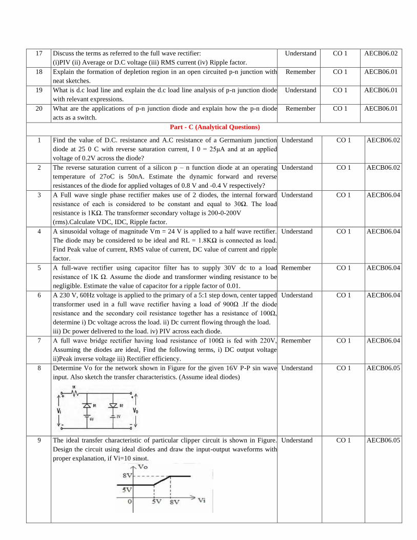
8 Determine Vo for the network shown in Figure for the given 16V P-P sin wave
input. Also sketch the transfer characteristics. (Assume ideal diodes)
Understand CO 1 AECB06.05
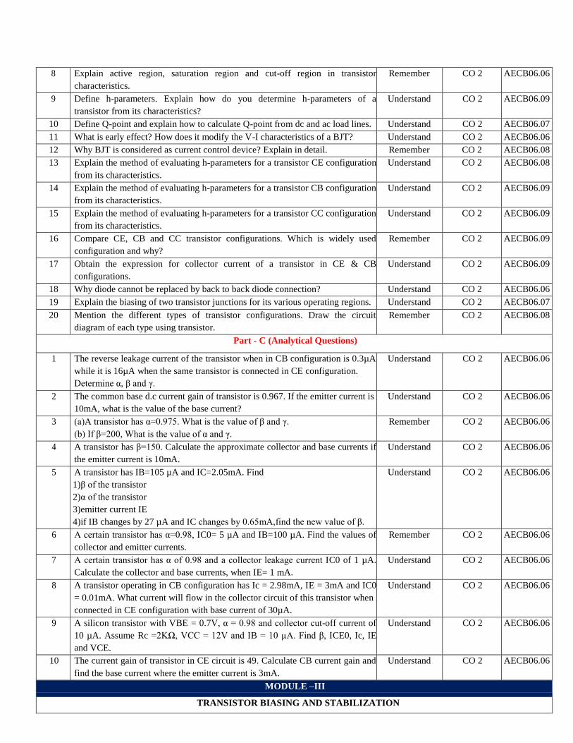
9 The ideal transfer characteristic of particular clipper circuit is shown in Figure.
Design the circuit using ideal diodes and draw the input-output waveforms with
proper explanation, if Vi=10 sinωt.
Understand CO 1 AECB06.05

10 For the circuit shown in Figure, a sine wave input of 100V peak is applied.
Sketch the output voltage V to the same time scale &transfer characteristic.
Assume ideal diodes.
Remember CO 1 AECB06.05
MODULE -II
BIPOLAR JUNCTION TRANSISTOR (BJT)
Part – A (Short Answer Questions)
1 Define Transistor? Remember CO 2 AECB06.06
2 What is meant by operating point Q? Understand CO 2 AECB06.06
3 Draw the symbols of NPN and PNP transistor? Understand CO 2 AECB06.06
4 Draw and explain the ac load line? Understand CO 2 AECB06.07
5 Compare CE,CC and CB configurations Remember CO 2 AECB06.08
6 Draw h parameters in CE configuration? Remember CO 2 AECB06.09
7 Draw h parameters in CB configuration? Remember CO 2 AECB06.09
8 What is meant by base width modulation? Remember CO 2 AECB06.06
9 Draw h parameters in CC configuration? Remember CO 2 AECB06.09
10 Define current amplification factor for CE configuration? Remember CO 2 AECB06.06
11 When the transistor is said to be in cut-off region? Understand CO 2 AECB06.06
12 List the various regions in a transistor and compare them with respect to doping
and width.
Understand CO 2 AECB06.06
13 Draw the output characteristics of NPN transistor in CE configuration? Understand CO 2 AECB06.06
14 Draw the circuit of a CB transistor in saturation region? Remember CO 2 AECB06.06
15 Write the relation between IC, β, IB and ICBO in a BJT? Remember CO 2 AECB06.06
16 Write the relation between α, β and γ in a BJT? Remember CO 2 AECB06.06
17 Draw the circuit of a CE transistor in active region? Remember CO 2 AECB06.06
18 Describes the various current components in a BJT? Remember CO 2 AECB06.06
19 Define Q-point? Remember CO 2 AECB06.06
20 Explain the concept of dc load line with the help of neat diagram? Remember CO 2 AECB06.07
Part - B (Long Answer Questions)
1 With a neat diagram explain the various current components in an NPN bipolar
junction transistor & hence derive general equation for collector current, IC?
Remember CO 2 AECB06.06
2 Define Early-effect. Explain why it is called as base-width modulation? Discuss
its consequences in transistors in detail?
Remember CO 2 AECB06.06
3 Explain working of transistor in common emitter configurations and draw its
input and output characteristics.
Understand CO 2 AECB06.08
4 Explain working of transistor in common base configurations and draw its input
and output characteristics.
Understand CO 2 AECB06.08
5 Explain working of transistor in common collector configurations and draw its
input and output characteristics.
Understand CO 2 AECB06.08
6 Define h-parameters of a transistor in a small signal model. What are the
benefits of h-parameters?
Remember CO 2 AECB06.09
7 Explain the constructional details of bipolar Junction Transistor? Understand CO 2 AECB06.06
8 Explain active region, saturation region and cut-off region in transistor
characteristics.
Remember CO 2 AECB06.06
9 Define h-parameters. Explain how do you determine h-parameters of a
transistor from its characteristics?
Understand CO 2 AECB06.09
10 Define Q-point and explain how to calculate Q-point from dc and ac load lines. Understand CO 2 AECB06.07
11 What is early effect? How does it modify the V-I characteristics of a BJT? Understand CO 2 AECB06.06
12 Why BJT is considered as current control device? Explain in detail. Remember CO 2 AECB06.08
13 Explain the method of evaluating h-parameters for a transistor CE configuration
from its characteristics.
Understand CO 2 AECB06.08
14 Explain the method of evaluating h-parameters for a transistor CB configuration
from its characteristics.
Understand CO 2 AECB06.09
15 Explain the method of evaluating h-parameters for a transistor CC configuration
from its characteristics.
Understand CO 2 AECB06.09
16 Compare CE, CB and CC transistor configurations. Which is widely used
configuration and why?
Remember CO 2 AECB06.09
17 Obtain the expression for collector current of a transistor in CE & CB
configurations.
Understand CO 2 AECB06.09
18 Why diode cannot be replaced by back to back diode connection? Understand CO 2 AECB06.06
19 Explain the biasing of two transistor junctions for its various operating regions. Understand CO 2 AECB06.07
20 Mention the different types of transistor configurations. Draw the circuit
diagram of each type using transistor.
Remember CO 2 AECB06.08
Part - C (Analytical Questions)
1 The reverse leakage current of the transistor when in CB configuration is 0.3µA
while it is 16µA when the same transistor is connected in CE configuration.
Determine α, β and γ.
Understand CO 2 AECB06.06
2 The common base d.c current gain of transistor is 0.967. If the emitter current is
10mA, what is the value of the base current?
Understand CO 2 AECB06.06
3 (a)A transistor has α=0.975. What is the value of β and γ.
(b) If β=200, What is the value of α and γ.
Remember CO 2 AECB06.06
4 A transistor has β=150. Calculate the approximate collector and base currents if
the emitter current is 10mA.
Understand CO 2 AECB06.06
5 A transistor has IB=105 µA and IC=2.05mA. Find
1)β of the transistor
2)α of the transistor
3)emitter current IE
4)if IB changes by 27 µA and IC changes by 0.65mA,find the new value of β.
Understand CO 2 AECB06.06
6 A certain transistor has α=0.98, IC0= 5 µA and IB=100 µA. Find the values of
collector and emitter currents.
Remember CO 2 AECB06.06
7 A certain transistor has α of 0.98 and a collector leakage current IC0 of 1 µA.
Calculate the collector and base currents, when IE= 1 mA.
Understand CO 2 AECB06.06
8 A transistor operating in CB configuration has Ic = 2.98mA, IE = 3mA and IC0
= 0.01mA. What current will flow in the collector circuit of this transistor when
connected in CE configuration with base current of 30µA.
Understand CO 2 AECB06.06
9 A silicon transistor with VBE = 0.7V, α = 0.98 and collector cut-off current of
10 µA. Assume Rc =2KΩ, VCC = 12V and IB = 10 µA. Find β, ICE0, Ic, IE
and VCE.
Understand CO 2 AECB06.06
10 The current gain of transistor in CE circuit is 49. Calculate CB current gain and
find the base current where the emitter current is 3mA.
Understand CO 2 AECB06.06
MODULE –III
TRANSISTOR BIASING AND STABILIZATION
Part – A (Short Answer Questions)
1 Define biasing? Remember CO 3 AECB06.11
2 Why biasing is necessary in BJT amplifiers? Remember CO 3 AECB06.11
3 Define three stability factors? Remember CO 3 AECB06.11
4 Which biasing method provides more stabilization amongst the three types of
biasing methods?
Understand CO 3 AECB06.11
5 Compare the advantages and disadvantages of biasing schemes? Remember CO 3 AECB06.11
6 Draw the circuit diagram of a collector to base biasing circuit of CE amplifier? Remember CO 3 AECB06.11
7 Write advantages of fixed bias circuitry? Understand CO 3 AECB06.11
8 Draw the circuit diagram of a fixed bias circuit of CE amplifier? Remember CO 3 AECB06.11
9 Draw a circuit employing a sensistor compensation? Remember CO 3 AECB06.12
10 Write down disadvantages of fixed bias circuit? Remember CO 3 AECB06.11
11 Define thermal runaway? Remember CO 3 AECB06.12
12 Define thermal resistance? Remember CO 3 AECB06.12
13 Define stability factors s and s‟. Remember CO 3 AECB06.11
14 Define thermal stability Remember CO 3 AECB06.12
15 List out the different types of biasing methods? Remember CO 3 AECB06.11
16 Differentiate bias stabilization and compensation techniques? Remember CO 3 AECB06.12
1 Write the expressions for AV and Ri of a CE amplifier. Remember CO 3 AECB06.14
2 Write the expressions for AV and Ri of a CB amplifier. Remember CO 3 AECB06.14
3 Write the expressions for AV and Ri of a CC amplifier. Remember CO 3 AECB06.14
4 What is the effect of bypass capacitor? Understand CO 3 AECB06.15
5 What is the effect of coupling capacitor? Understand CO 3 AECB06.15
6 Write the expressions for AI and Rout of a CE amplifier signals Remember CO 3 AECB06.13
7 Draw the frequency response of BJT amplifier. Remember CO 3 AECB06.14
8 Write the expressions for AI and Rout of a CB amplifier signals Remember CO 3 AECB06.12
9 Write the expressions for AI and Rout of a CC amplifier signals Remember CO 3 AECB06.12
10 Write the expressions for AVS and AIS of a CE amplifier. Remember CO 3 AECB06.12
Part – B (Long Answer Questions)
1 Draw the circuit diagram of a voltage divider bias and derive the expression for
stability factor.
Remember CO 3 AECB06.11
2 Draw the circuit diagram of a fixed bias and derive the expression for stability
factor.
Understand CO 3 AECB06.11
3 Draw the circuit diagram of a collector to base bias and derive expression for
stability factor.
Remember CO 3 AECB06.11
4 List the three sources of instability of collector current and hence define the
three stability factors.
Remember CO 3 AECB06.11
5 Explain thermal runaway. What are the factors effecting the stability factor. Remember CO 3 AECB06.12
6 What is the necessity of biasing circuits? Explain bias compensation using
diodes and transistors.
Understand CO 3 AECB06.12
7 Which biasing method provides more stabilization than the three types of
biasing methods? Why?
Understand CO 3 AECB06.12
8 For the improvement of stability of the operating point what suggestions you
make for self bias. Discuss with the help of stability factors.
Understand CO 3 AECB06.11
9 What do you understand by bias stabilization and bias compensation? Why it is
necessary in transistor amplifiers?
Understand CO 3 AECB06.12
10 Explain the concept of d.c load line in BJT with the help of diagram. What are
the requirements of biasing?
Understand CO 3 AECB06.11
1 Draw the circuit diagram of CE amplifier using hybrid parameters and derive
the expression for AI , AV, Ri and Ro.
Understand CO 3 AECB06.14
2 Draw the circuit diagram of CB amplifier using hybrid parameters and derive
the expression for AI , AV, Ri and Ro.
Remember CO 3 AECB06.14
3 Draw the circuit diagram of CC amplifier using hybrid parameters and derive
the expression for AI , AV, Ri and Ro.
Understand CO 3 AECB06.14
4 Draw the frequency response of BJT amplifier and explain the effect of bypass
capacitor on the frequency response in detail.
Remember CO 3 AECB06.15
5 Draw the frequency response of BJT amplifier and explain the effect of
coupling capacitor on the frequency response in detail.
Understand CO 3 AECB06.15
6 Draw the circuit diagram of CE amplifier with emitter resistance and derive the
expression for AI, AV, Ri and Ro using hybrid model.
Remember CO 3 AECB06.13
7 Give the comparison between CB, CE and CC amplifiers in terms of current
gain, voltage gain, input impedance and output admittance.
Remember CO 3 AECB06.15
8 Write a short note on how the transistor acts as an amplifier. Remember CO 3 AECB06.13
9 For three configurations of a BJT, we require three different sets of h-
parameters. Justify your answer.
Remember CO 3 AECB06.13
10 What do you understand by the term ‘equivalent circuit’ of a transistor? Draw
the equivalent circuit of the generalized transistor amplifier and explain the
significance of each parameter.
Remember CO 3 AECB06.13
Part - C (Analytical Questions)
1 In a Silicon transistor circuit with a fixed bias, Vcc = 9V, RC = 3KΩ, RB=8KΩ,
β = 50, VBE = 0.7V. Find the operating point and stability factor.
Understand CO 3 AECB06.11
2 In a Silicon transistor circuit with a fixed bias, Vcc =25V, RC =820Ω, RB
=180KΩ, β = 80, VBE = 0.7V. Determine the values of base current, emitter
current and the collector to emitter voltage.
Remember CO 3 AECB06.11
3 In a Silicon transistor circuit with a fixed bias, Vcc =12V, RC =330Ω,
IB=0.3mA, β = 100, VBE = 0.7V. Determine the value of bias resistor RB and
Stability factor.
Understand CO 3 AECB06.11
4 In a Silicon transistor circuit with a collector to base bias, Vcc =10V, RC =
10KΩ, RB =100KΩ, β = 100, VBE = 0.7V. Calculate the operating point and
also draw the load line and locate Q point on it.
Remember CO 3 AECB06.11
5 An NPN transistor with β =50 is used in a common emitter circuit with
Vcc=10V, Rc=2K Ω. The bias is obtained by connecting a 100K Ω resistance
from collector to base. Assume VBE=0.7V. Find
(a) The quiescent point
(b) The stability factor S.
Understand CO 3 AECB06.11
6 Determine the quiescent currents and the collector to emitter voltage for a
germanium transistor with β=50 in self-biasing arrangement. Draw the circuit
with a given component values Vcc=20V, Rc=2KΩ, Re=100Ω, R1=100K Ω,
R2=5K Ω. Also find the stability factor.
Remember CO 3 AECB06.12
7 Design a self-bias circuit as per the following specifications. Vcc =12V,
Vce=2V, Ic=4mA, hfe=80. Draw the complete diagram with the designed
values.
Understand CO 3 AECB06.11
1 The hybrid parameters for a transistor used in CE configuration are hie = 5kΩ;
hfe = 180; hre = 1.25 × 10⁻⁴; hoe = 16 × 10-6 ohms. The transistor has a load
resistance of 20 KΩ in the collector and is supplied from a signal source of
resistance 5 KΩ. Compute the value of input impedance, output impedance,
current gain and voltage gain.
Understand CO 3 AECB06.13
2 A CE amplifier with emitter resistor RE=800Ω, RL=1k Ω. Given the h-
parameters of CE configuration are hie=1.1KΩ, hre=5*10-4, hfe=50,
hoe=25µA/V. Compute AI, AV, AIs, Ri, Ro.
Remember CO 3 AECB06.14
3 A CE amplifier is driven by voltage source with internal resistance Rs=800Ω.
The load impedance RL=2k Ω. The h-parameters are hie=1.1KΩ, hre=2.5*10-4,
hfe=50, hoe=25µA/V. Compute AI, AV, AIs, Ri, and Zo.
Understand CO 3 AECB06.14
4 A CB amplifier is driven by voltage source with internal resistance Rs=800Ω.
The load impedance RL=2k Ω. The h-parameters are hib=22 Ω, hrb=3*10-4,
hfb=-0.98, hoe=0.5µA/V. Compute AI, AV, AIs, Ri, Zo & Ap.
Remember CO 3 AECB06.14
5 A CC amplifier is driven by voltage source with internal resistance
Rs=800Ω.The load impedance RL=2k Ω. The h-parameters are hic=1.1KΩ,
hrc=1, hfc = -51, hoc = 25µA/V. Compute AI, AV, AIs, Ri, Zo & Ap.
Understand CO 3 AECB06.14
MODULE -IV
JUNCTION FIELD EFFECT TRANSISTOR
Part – A (Short Answer Questions)
1 Why FET is called as unipolar device? Understand CO 4 AECB06.17
2 Why do you call FET as field effect transistor? Understand CO 4 AECB06.16
3 Write down the relationship between various FET parameters? Remember CO 4 AECB06.17
4 Why the input impedance of FET is more than that of a BJT? Understand CO 4 AECB06.18
5 Why N channel FET’s are preferred over P channel FET’s? Understand CO 4 AECB06.17
6 Give the drain current equation of JFET. Remember CO 4 AECB06.16
7 What are the parameters of JFET? Remember CO 4 AECB06.17
8 Mention the operating modes of FET. Remember CO 4 AECB06.20
9 Define the amplification factor in the JFET Remember CO 4 AECB06.17
10 What are the operating regions of a JFET? Remember CO 4 AECB06.17
11 Why FET is called a voltage controlled device? Understand CO 4 AECB06.18
12 What is a FET? Remember CO 4 AECB06.17
13 Draw the symbol for i) P-channel JFET, ii) N-channel JFET Remember CO 4 AECB06.19
14 List the advantages of FET Remember CO 4 AECB06.17
15 Draw the drain characteristics curves of an n-channel JFET? Remember CO 4 AECB06.19
16 What are the special features of FET? Remember CO 4 AECB06.17
17 Define pinch off voltage? Remember CO 4 AECB06.18
18 Define rd and gm? Remember CO 4 AECB06.17
19 Draw the transfer characteristics curves of an n-channel JFET? Remember CO 4 AECB06.20
20 What are the main draw backs of FET? Understand CO 4 AECB06.17
Part – B (Long Answer Questions)
1 Explain the operation of JFET and derive the drain and transfer characteristics. Understand CO 4 AECB06.17
2 With neat sketches explain the construction, principle of operation, and
characteristics of an n-channel JFET.
Understand CO 4 AECB06.20
3 Explain the construction and operation of p-channel JFET. Understand CO 4 AECB06.20
4 Compare JFET with BJT. Understand CO 4 AECB06.18
5 How a FET can be used as voltage variable resistance (VVR)? Understand CO 4 AECB06.17
6 Create a relation between the three JFET parameters? Understand CO 4 AECB06.17
7 Using the basic structure of JFET. Explain its physical operation and draw its
output characteristics. Give expression for drain current.
Understand CO 4 AECB06.20
8 Obtain the expression for the pinch off voltage VP in the case of n-channel
JFET.
Understand CO 4 AECB06.17
9 Explain voltage divider biasing in FET. Understand CO 4 AECB06.20
10 Draw the fixed bias and self bias circuit using FET. Explain in detail. Understand CO 4 AECB06.20

11 With neat sketches explain the construction, principle of operation, and
characteristics of P-channel JFET.
Remember CO 4 AECB06.17
12 What are the main constructional differences between a MOSFET and a BJT?
What effect do they have on the current conduction mechanism of a MOSFET?
Understand CO 4 AECB06.17
13 List out the differences between BJT and FET. Remember CO 4 AECB06.17
14 Compare enhancement and depletion modes of a MOSFET with the help of its
characteristics and construction?
Understand CO 4 AECB06.18
15 With the help of neat sketches and characteristic curves explain the construction
& operation of a JFET and mark the regions of operation on the characteristics?
Remember CO 4 AECB06.18
16 Explain constructional features of a JFET. Understand CO 4 AECB06.17
17 Explain the construction & operation of a N-channel MOSFET in enhancement
and depletion modes with the help of static drain characteristics and transfer
characteristics?
Remember CO 4 AECB06.19
18 Explain the construction & operation of a P-channel MOSFET in enhancement
and depletion modes with the help of static drain characteristics and transfer
characteristics?
Understand CO 4 AECB06.17
19 Sketch the drain characteristics of MOSFET for different values of VGS &
mark different regions of operation.
Remember CO 4 AECB06.19
20 List any four merits of MOSFET to show that they are more suitable than
JFETS in Integrated circuits?
Remember CO 4 AECB06.20
Part - C (Analytical Questions)
1 In a n-channel JFET, IDSS = 20 m A and VP = -6 V. Calculate the drain current
when VGS = -3 V.
Evaluate CO 4 AECB06.17
2 Determine the transconductance of a JFET if its amplification factor is 96 and
drain resistance is 32 KΩ.
Evaluate CO 4 AECB06.17
3 An N-channel JFET has IDSS = 8 mA and VP = -5V. Determine the minimum
value of VDS for pinch-off region and the drain current IDS for VGS = -2V in
the pinch-off region.
Evaluate CO 4 AECB06.17
4 A JFET has parameters of VGS(off) is -20V and IDSS is 12mA. Find ID for the
device using VGS = 0V.
Evaluate CO 4 AECB06.17
5 The following information is included on the data sheets for an N-channel
JFET. IDSS = 20mA, VP = -8V and gm0 = 5000us. Determine the values of
transconductance at VGS = -4V.
Evaluate CO 4 AECB06.17
6 Compare Depletion MOSFET and enhancement MOSFET. Also Derive the
expression for transconductance in a CS field effect transistor.
Remember CO 4 AECB06.18
7 A common source MOSFET amplifier is to be constructed using a n-channel
MOSFET which has a conduction parameter of 50mA/V and a threshold
voltage of 2.0 volts. If the supply voltage is +15 volts and the load resistor is
470 Ohms, calculate the values of the resistors required to bias the MOSFET
amplifier at 1/3(VDD). Draw the circuit diagram and Values
given: VDD = +15v, VTH = +2.0v, k = 50mA/V2 and RD = 470Ω.
Remember CO 4 AECB06.19
8 The following information is included on the data sheets for an N-channel
JFET. IDSS = 25mA, VP = -10V and gm0 = 4000us. Determine the values of
transconductance at VGS = -5V.
Remember CO 4 AECB06.19
9 Explain the construction and principle of operation of Depletion type P-channel
MOSFET.
Understand CO 4 AECB06.17
10 Explain the construction and principle of operation of Enhancement type P-
channel MOSFET.
Understand CO 4 AECB06.17
MODULE -V
FET AMPLIFIERS

Part - A (Short Answer Questions)
1 Give small signal model of JEFT Understand CO 5 AECB06.21
2 List the important features of FET? Remember CO 5 AECB06.21
3 Draw the functional diagram of JFET? Understand CO 5 AECB06.21
4 Define pinch off voltage? Understand CO 5 AECB06.17
5 List the applications of Zener diode? Remember CO 5 AECB06.24
6 Define rd and gm? Understand CO 5 AECB06.21
7 Write the differences between avalanche and Zener breakdown mechanisms? Remember CO 5 AECB06.24
8 Draw the two transistor equivalent circuit of a SCR Understand CO 5 AECB06.25
9 Draw the V-I characteristics of SCR? Understand CO 5 AECB06.25
10 List the applications of varactor diode? Remember CO 5 AECB06.25
11 Explain why a SCR is operated only in the forward biased condition? Understand CO 5 AECB06.25
12 Explain about ohmic and saturation regions? Understand CO 5 AECB06.22
13 Draw the drain characteristics of an n-channel enhancement type MOSFET? Understand CO 5 AECB06.23
14 Draw the equivalent circuit of a UJT Understand CO 5 AECB06.25
15 Write down applications of UJT? Understand CO 5 AECB06.25
16 What is meant by tunnel diode? Remember CO 5 AECB06.24
17 Draw the VI characteristics of tunnel diode. Understand CO 5 AECB06.24
18 List out the applications of tunnel diode Remember CO 5 AECB06.24
19 What is meant by SCR? Understand CO 5 AECB06.25
20 List out the advantages of SCR. Remember CO 5 AECB06.25
Part - B (Long Answer Questions)
1 Give the construction details of UJT & explain its operation with the help of
equivalent circuits?
Remember CO 5 AECB06.25
2 Explain the operation of FET with its characteristics and explain the different
regions in transfer characteristics?
Understand CO 5 AECB06.21
3 Create a relation between the three JFET parameters, µ, r d and gm? Understand CO 5 AECB06.21
4 Explain the construction & operation of a P-channel MOSFET in enhancement
and depletion modes with the help of static drain characteristics and transfer
characteristics?
Remember CO 5 AECB06.23
5 Draw the small-signal model of common drain FET amplifier. Derive
expressions for voltage gain and output resistance?
Understand CO 5 AECB06.22
6 Explain the tunneling phenomenon. Explain the characteristics of tunnel diode
with the help of necessary energy band diagrams?
Understand CO 5 AECB06.25
7 Sketch the static characteristics and firing characteristics of SCR and explain
the shape of the curve?
Remember CO 5 AECB06.25
8 Explain how a variable capacitance can be built using a varactor diode? Remember CO 5 AECB06.25
9 Explain the V-I characteristics of Zener diode and distinguish between
Avalanche and Zener Break downs?
Understand CO 5 AECB06.24
10 Draw the small-signal model of common gate FET amplifier. Derive
expressions for voltage gain and output resistance?
Remember CO 5 AECB06.23
11 Draw the small-signal model of common drain FET amplifier. Derive
expressions for voltage gain and output resistance?
Remember CO 5 AECB06.23
12 Draw the small-signal model of common source FET amplifier. Derive
expressions for voltage gain and output resistance?
Understand CO 5 AECB06.23
13 Describe the operation of UJT and sketch its characteristics. Remember CO 5 AECB06.24
14 Discuss the operation of varactor diode and list out its application. Remember CO 5 AECB06.24
15 Describe the working principle of SCR with VI characteristics. Understand CO 5 AECB06.25
16 Sketch the V-I characteristics of zener diode for forward bias and reverse bias
voltages.
Remember CO 5 AECB06.25

17 Compare zener diode and the conventional p-n junction diode. Remember CO 5 AECB06.24
18 Draw the basic structure of a SCR and explain its characteristics. Understand CO 5 AECB06.25
19 Discuss the working principle of a varactor diode and explain its characteristics. Remember CO 5 AECB06.25
20 Explain the V-I characteristics of tunnel diode with negative resistance region.
State the applications of tunnel diode.
Remember CO 5 AECB06.24
Part - C (Analytical Questions)
1 A 5.0V stabilized power supply is required to be produced from a 12V
DC power supply input source. The maximum power rating PZ of the zener
diode is 2W. Using the zener regulator circuit above calculate: a) The
maximum current flowing through the zener diode. b) The minimum value of
the series resistor, RS. c) The load current IL if a load resistor of 1kΩ is
connected across the zener diode. d) The zener current IZ at full load.
Remember CO 5 AECB06.24
2 Define the three FET parameters: gm, rd and µ. Prove that µ=gm x rd. Understand CO 5 AECB06.21
3 In an n-channel FET, the effective channel width is 3x 10⁻⁴cm and the donor
impurity concentration is 1015 electrons/cm3. Find the pinch-off voltage?
Understand CO 5 AECB06.21
4 A Common Source FET amplifier circuit with un bypassed Rs has the following
circuit parameters: Rd = 15K, RS = 0.5K, Rg = 1M, rd = 5K, gm= 5mS and
VDD = 20 V. Determine AV& RO?
Understand CO 5 AECB06.22
5 A self-biased p – channel JFET has a pinch – off voltage of VP = 5 V and IDSS
= 12 mA. The supply voltage is 12 V. Determine the values of RD and RS so
that ID = 5 mA and VDS = 6V?
Remember CO 5 AECB06.22
6 For the Zener diode circuit shown in Figure, determine VL, VR, IZ & R?
Understand CO 5 AECB06.24
7 The data sheet for a 2N2646 Uni junction Transistor gives the intrinsic stand-
off ratio η as 0.65. If a 100nF capacitor is used to generate the timing pulses,
calculate the timing resistor required to produce an oscillation frequency of
100Hz. A). The timing period. B) The value of the timing resistor, R3.
Remember CO 5 AECB06.25
8 Explain the construction and principle of operation of Depletion type N-
channel MOSFET.
Remember CO 5 AECB06.23
9 A Zener voltage regulator circuit is to maintain constant voltage at 60 V, over
a current range from 5 to 50 mA. The input supply voltage is 200 V.
Determine the value of resistance R to be connected in the circuit, for voltage
regulation from load current IL = 0 mA to IL max, the maximum possible
value of IL. What is the value IL max?
Remember CO 5 AECB06.24
10 Compare Depletion MOSFET and enhancement MOSFET. Also Derive the
expression for transconductance in a field effect transistor.
Understand CO 5 AECB06.23
Prepared by: Mr. D.Khalandar Basha, Assistant professor
Mrs. G.Mary swarna latha, Assistant professor
Mrs. M.Sreevani, Assistant professor
HOD, ECE