instrumentation departmentjohn coughlan et al.rutherford appleton laboratory23 october 2002tracker...
TRANSCRIPT

Instrumentation Department John Coughlan et al.Rutherford Appleton Laboratory 23 October 2002Tracker Electronics Meeting
The Front-End Driver Card FEDv1
•VME crate requirements definition
•FEDv1 status :
Hardware
Firmware & low-level software
•FEDv1 testing plans
http://www.te.rl.ac.uk/esdg/cms-fed/index.html

Instrumentation Department John Coughlan et al.Rutherford Appleton Laboratory 23 October 2002Tracker Electronics Meeting
FEDv1 CratesRequirements Document
•Requirements needed for Tracker Crate ordering
•Aim to have common VME64x bus crates for FED and FEC
•List of special needs, connectors, power…etc.
•E.g. FED may require Transition cards (DAQ links)
•References to LHC Crate technical specification EP document
•Released for comments
Instrumentation Department John Coughlan et al.Rutherford Appleton Laboratory 23 October 2002Tracker Electronics Meeting
FEDv1 CratesRequirements Document
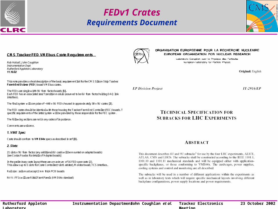
CMS Tracker FED VMEbus Crate Requirements
Rob Halsall, John CoughlanInstrumentation DeptRutherford Appleton Laboratory11.10.02
This note provides a short description of the basic requirement list for the CMS Silicon Strip TrackerFront-End Driver (FED) board VMEbus crates.
The FEDs are single width 9U form factor boards [1].Each FED has an associated rear Transition module (assumed to be 6U form factor holding DAQ linkinterface).
The final system will comprise of ~440 x 9U FEDs housed in approximately 30 x 9U crates [2].
The FED crates should be identical with those housing the Tracker Front-End Controller (FEC) boards. Thespecific requirements of the latter system will be provided by those responsible for the FEC system.
The following sections are not in any order of importance.
Comments are welcome.
1. VME Spec:
Crate should conform to VME64x specs as described in ref [3].
2. Slots:
21 slots x 9U form factor (any additional 6U cards will be mounted on adapter boards)[see Costas Foudas for details of Adapter boards]
In the preliminary crate layout there are a maximum of 16 FEDs per crate [2].This allows up to 5 slots for Crate Controller(=slot1 arbiter), Monitor board, TCS interface…
Rail size : rails must accept 2 mm thick PCB boards
NOTE: FF1s will use Rittal Front Panels (VME64x standard)

Instrumentation Department John Coughlan et al.Rutherford Appleton Laboratory 23 October 2002Tracker Electronics Meeting
FEDv1 Overview
VME-FPGA
TTCrx
BE-FPGAEvent Builder
Buffers
FPGAConfiguration
Compact Flash
PowerDC-DC
DAQInterface
12
12
12
12
12
12
12
12
Front-End Modules x 8Double-sided board
CERNOpto-
Rx Analogue/Digital
96 TrackerOpto Fibres
VMEInterface
XilinxVirtex-IIFPGA
Modularity
9U VME64x Form Factor
Modularity matches Opto Links
8 x Front-End “modules”
OptoRx/Digitisation/Cluster Finding
Back-End module / Event Builder
VME module / Configuration
Power module
Other Interfaces:
TTC : Clk / L1 / BX
DAQ : Fast Readout Link
TCS : Busy & Throttle
VME : Control & Monitoring
JTAG : Test & Configuration
FE-FPGAClusterFinder
TTC
TCS
TempMonitor
JTAG
TCS : Trigger Control System
9U VME64x

Instrumentation Department John Coughlan et al.Rutherford Appleton Laboratory 23 October 2002Tracker Electronics Meeting
FEDv1 Project History
VME-FPGA
TTCrx
BE-FPGAEvent Builder
Buffers
FPGAConfiguration
Compact Flash
PowerDC-DC
DAQInterface
12
12
12
12
12
12
12
12
Front-End Modules x 8Double-sided board
CERNOpto-
Rx Analogue/Digital
96 TrackerOpto Fibres
VMEInterface
XilinxVirtex-IIFPGA
Analogue Circuit for signal match from OptoRx to ADCs
(good working relationship with Francois&Jan)
Fit 96 ADC channels on board
FPGAs choice of Xilinx Virtex-II family. Fitting FE design into target part.
But progress (always) take longer than you think…
S-LINK Transition card / Direct?
Power & VME modules took more time than anticipated
FPGA de-coupling schemes.
+ many minor design decisions.
~ 1Q behind schedule May 2002
FE-FPGAClusterFinder
TTC
TCS
TempMonitor
JTAG
TCS : Trigger Control System
9U VME64x

Instrumentation Department John Coughlan et al.Rutherford Appleton Laboratory 23 October 2002Tracker Electronics Meeting
FEDv1 Board Layout Primary Side
•Complex board•Pushing density limits•Analogue & Digital• & signal integrity

Instrumentation Department John Coughlan et al.Rutherford Appleton Laboratory 23 October 2002Tracker Electronics Meeting
FED v1 Board Layout Secondary Side
View thru the board
Double sided

Instrumentation Department John Coughlan et al.Rutherford Appleton Laboratory 23 October 2002Tracker Electronics Meeting
FEDv1 Overview
12
12
12
12
12
12
12
12
Front-End Modules x 8Double-sided board
CERNOpto-
Rx Analogue/Digital
96 TrackerOpto Fibres
XilinxVirtex-IIFPGA
Modularity
8 x Front-End “modules”
FE-FPGAClusterFinder
9U VME64x

Instrumentation Department John Coughlan et al.Rutherford Appleton Laboratory 23 October 2002Tracker Electronics Meeting
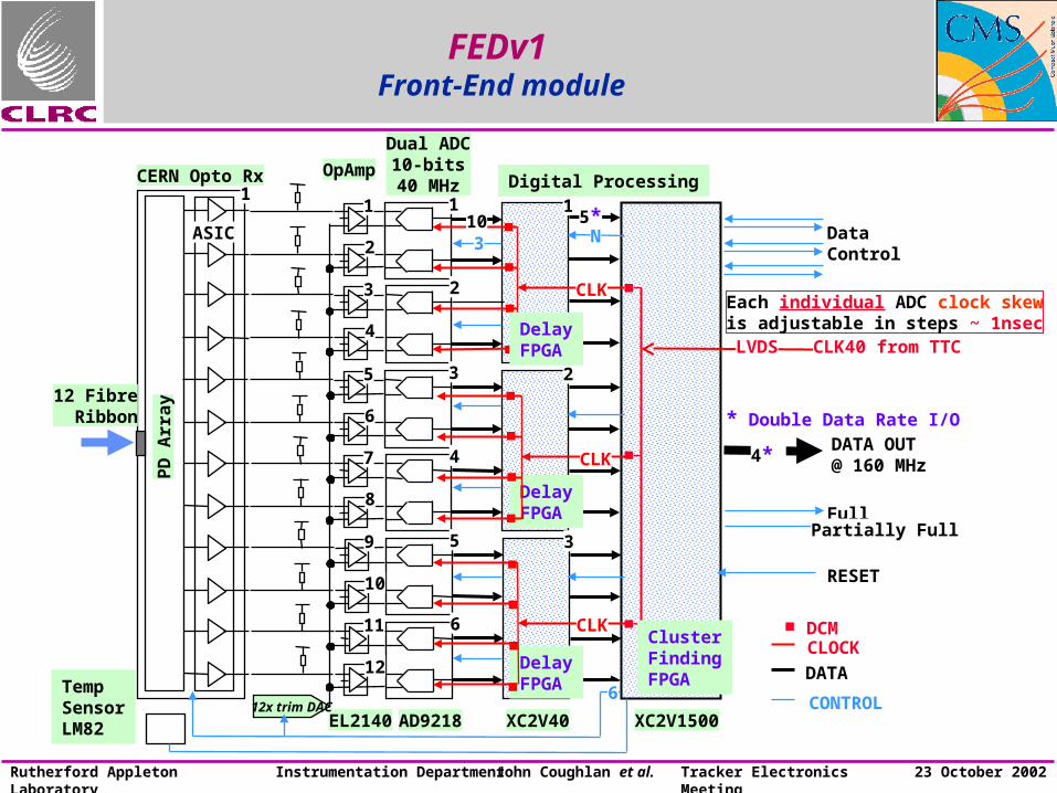
FEDv1 Front-End module
12 FibreRibbon
PD
Arr
ay
111
2
1
23
4
35
6
2
47
8
59
10
3
611
12
5*
CLK
DCM
LVDS CLK40 from TTC
CERN Opto Rx
6
CLOCK
CONTROL
DATA
DATA OUT@ 160 MHz
3 N
FullPartially Full
RESET
ClusterFindingFPGA
DelayFPGA
DelayFPGA
DelayFPGA
Dual ADC10-bits40 MHz
OpAmp
XC2V1500XC2V40AD9218EL2140
CLK
CLK
10ASIC
4*
DataControl
Digital Processing
12x trim DAC
TempSensorLM82
* Double Data Rate I/O
Each individual ADC clock skewis adjustable in steps ~ 1nsec

Instrumentation Department John Coughlan et al.Rutherford Appleton Laboratory 23 October 2002Tracker Electronics Meeting
FEDv1 Front-End module Primary Routed
Note: FPGA de-coupling
OptoRx ADCs 40K FPGAs 1500K FPGAOpAmps
12 optical channels Dense circuitry

Instrumentation Department John Coughlan et al.Rutherford Appleton Laboratory 23 October 2002Tracker Electronics Meeting
FEDv1 Front-End module Secondary Routed
Double-sided

Instrumentation Department John Coughlan et al.Rutherford Appleton Laboratory 23 October 2002Tracker Electronics Meeting
FEDv1 Full-Scale 9U Layout
TTCrx
BE-FPGAEvent Builder
Buffers
DAQInterface
12
12
12
12
12
12
12
12
Front-End Modules x 8Double-sided board
CERNOpto-
Rx Analogue/Digital
96 TrackerOpto Fibres
XilinxVirtex-IIFPGA
Back-End module
For each L1-Trigger:
Collects 8 x FE variable length data fragments
Formats FED event for DAQ
Appends TTC synch information
Buffers in External QDR SRAM
Sends data via DAQ Front-end Readout Link FRL
Signals to TCS : Busy/Throttle
FE-FPGAClusterFinder
TTC
TCS
TCS : Trigger Control System
9U VME64x
PinDiode/Amp
ASIC

Instrumentation Department John Coughlan et al.Rutherford Appleton Laboratory 23 October 2002Tracker Electronics Meeting
DAQFront-endReadout
LinkFRL
DAQ MezzanineCard
Transition Card
BusyThrottle
S-LINK64
FEDv1 FED-DAQ Interface
TTCrx
BE-FPGAEvent Builder
Buffers
12
12
12
12
12
12
12
12
TTC
TCS
FRL DAQ links use S-LINK64 standardImplementation: Channel Link800 MBytes/sec max
Average DAQ rate 200 MBytes/sec
Due to mechanical constraints place DAQ link card on Transition card

Instrumentation Department John Coughlan et al.Rutherford Appleton Laboratory 23 October 2002Tracker Electronics Meeting
Alternative scheme:“Channel Link” inVirtex-II BE-FPGA
DAQ
FEDv1 FED-DAQ Interface (alternative)
TTCrx
BE-FPGAEvent Builder
Buffers
12
12
12
12
12
12
12
12
TTC
TCS

Instrumentation Department John Coughlan et al.Rutherford Appleton Laboratory 23 October 2002Tracker Electronics Meeting
FEDv1 VME module
VME-FPGAFPGA
Configuration
12
12
12
12
12
12
12
12
VMEInterface
XilinxVirtex-IIFPGA
VME Interface Minimum Features for 2003:
A32/D32 Slave access only
Possible Slave BLT32?
No DMA engine
No Interrupts
Possible 64x Dynamic Addressing?
FPGA Configuration:
Xilinx System ACE Compact Flash
MPU-VME interface for in-situ re-programming via Crate Controller
(Not in 2003?)
JTAG for Configuration & Test
JTAG
9U VME64x
System ACE CF

Instrumentation Department John Coughlan et al.Rutherford Appleton Laboratory 23 October 2002Tracker Electronics Meeting
FEDv1 Power module
PowerDC-DC
12
12
12
12
12
12
12
12
Front-End Modules x 8Double-sided board
CERNOpto-
Rx Analogue/Digital
XilinxVirtex-IIFPGA
Standard LHC spec crate supplies:
+3.3V, +5V, +12V
Derive: -5V, 1.5V, 2.5V on board
Board Estimate ~ 80 W
Hot Swap Controllers:
Electronic fuses
Protection against out of range voltage & current
Sequence power
Protections:
Over temperature shutdown
TempMonitor
TCS : Trigger Control System
9U VME64x
Warning

Instrumentation Department John Coughlan et al.Rutherford Appleton Laboratory 23 October 2002Tracker Electronics Meeting
FEDv1 Hardware Status
VME-FPGA
TTCrx
BE-FPGAEvent Builder
Buffers
FPGAConfiguration
PowerDC-DC
DAQInterface
12
12
12
12
12
12
12
12
Front-End Modules x 8Double-sided board
CERNOpto-
Rx Analogue/Digital
96 TrackerOpto Fibres
VMEInterface
XilinxVirtex-IIFPGA
FE-FPGAClusterFinder
TTC
TCS
TempMonitor
JTAG
TCS : Trigger Control System
9U VME64x
Hardware:Analogue Design CompleteDigital Design CompletePower Design CompleteFirmware:Cluster Finding CompleteEvent Building 50% DoneVME Interface 25% DoneBoard:Layout & Routing Front-End Module
CompleteBack-End Layout doneRouting started
Manufacture Tape out to PCB week 46Testing Start at RAL week 50
Board Status

Instrumentation Department John Coughlan et al.Rutherford Appleton Laboratory 23 October 2002Tracker Electronics Meeting
FED Schedule
Schedule
2002/Q4 : 2 x FEDv1 @ for UK test Batch 1*
2003/Q4 : ~10? x FEDv1 @ CERN Batch 2**
2004/Q4 : ~10? x FEDv2 manufacture
2005/Q2** : 500 x FEDv3 manufacture
(**funds permitting)
FEDv1 : Full scale PrototypeFEDv2 : Pre-productionFEDv3 : Final production
FEDv1 FEDv2
FEDv3
* OptoRx added post-assembly.
** Procurement started for critical parts for Batch 2

Instrumentation Department John Coughlan et al.Rutherford Appleton Laboratory 23 October 2002Tracker Electronics Meeting
FED TIB Test Schedule
Q. Deliver 2 x FEDv1 Batch 1.5 @ CERN for TIB test starting July 2003 ??
•Very tough. Testing is a big job. Can’t promise to deliver in June?
•Use Batch1 PCBs. ie No design iteration possible.
•Risk that design has major fault.
•Prioritise essential firmware and testing plan.
•Require explicit list of functionality essential for the TIB assembly centre.
FEDv1 FEDv2
FEDv3
TIB?
OptoRx?

Instrumentation Department John Coughlan et al.Rutherford Appleton Laboratory 23 October 2002Tracker Electronics Meeting
FEDv1Firmware & Low-Level Software

Instrumentation Department John Coughlan et al.Rutherford Appleton Laboratory 23 October 2002Tracker Electronics Meeting
FEDv1 Firmware & Software
VME-FPGA
TTCrx
BE-FPGAEvent Builder
Buffers
FPGAConfiguration
PowerDC-DC
DAQInterface
12
12
12
12
12
12
12
12
Front-End Modules x 8Double-sided board
CERNOpto-
Rx Analogue/Digital
96 TrackerOpto Fibres
VMEInterface
XilinxVirtex-IIFPGA
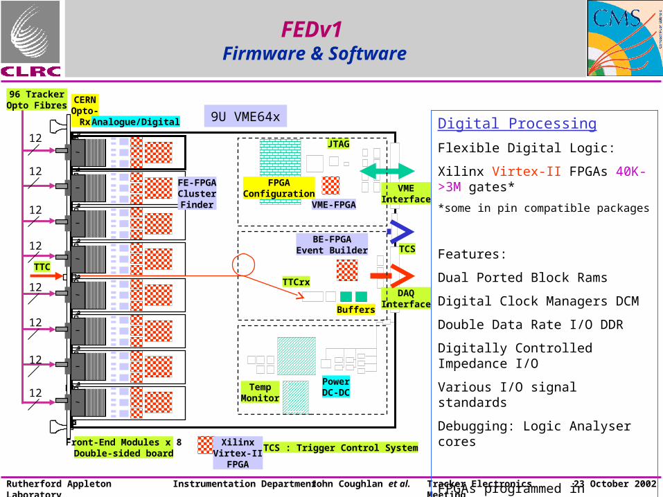
Digital Processing
Xilinx Virtex-II FPGAs 40K->3M gates
4 Species of FPGA:
Delay FPGA 40K: Clock skew +...
FE FPGA 1.5M: Cluster Finding +...
BE FPGA 2M: Event Building +...
VME FPGA 1M: VME Interface +...
in general one designer per species
FPGAs programmed in both
VHDL & VERILOG
FE-FPGAClusterFinder
TTC
TCS
TempMonitor
JTAG
TCS : Trigger Control System
9U VME64x
Instrumentation Department John Coughlan et al.Rutherford Appleton Laboratory 23 October 2002Tracker Electronics Meeting
FEDv1 Front-End module
12 FibreRibbon
PD
Arr
ay
111
2
1
23
4
35
6
2
47
8
59
10
3
611
12
5*
CLK
DCM
LVDS CLK40 from TTC
CERN Opto Rx
6
CLOCK
CONTROL
DATA
DATA OUT@ 160 MHz
3 N
FullPartially Full
RESET
ClusterFindingFPGA
DelayFPGA
DelayFPGA
DelayFPGA
Dual ADC10-bits40 MHz
OpAmp
XC2V1500XC2V40AD9218EL2140
CLK
CLK
10ASIC
4*
DataControl
Digital Processing
12x trim DAC
TempSensorLM82
* Double Data Rate I/O
Each individual ADC clock skewis adjustable in steps ~ 1nsec

Instrumentation Department John Coughlan et al.Rutherford Appleton Laboratory 23 October 2002Tracker Electronics Meeting
CMS Silicon Strip Tracker FED Front-End FPGA Logic
ADC 1 10 10
sy
nc
11
trig2
Pe
d s
ub
11
trig3
Re
-ord
er
cm
su
b
8
Hit
fin
din
g
s-datas-addr8
16
hit
Pa
ck
eti
se
r
4
averages 8header control
DP
M 16
No hits
Se
qu
en
ce
r-m
ux
8 8a
d
a
d
ADC 1210 10
trig1
sy
nc
11
trig2
Pe
d s
ub
11
trig3
Re
-ord
er
cm
su
b
8
Hit
fin
din
g
s-datas-addr8
16
256 cycles 256 cycles
hit DP
M 16
No hits
Se
qu
en
ce
r-m
ux
8 8a
d
a
d
status
averages8header status
nx256x16
trig4
Synch inSynch out
Sy
nc
h
emulator in
mu
x
Serial I/O
Se
ria
l In
t
B’Scan
Lo
ca
lIO
Config
Cluster Finding FPGA VERILOG Firmware
Full flags
data
Global reset
Co
ntr
ol
Sub resets
10
10
Ph
as
eR
eg
iste
rsP
ha
se
Re
gis
ters
2 x 256 cycles 256 cycles nx256x16
trig1Synch error
4x
Temp Sensor
Delay Line
Opto Rx
Clock 40 MHzD
LL
1x2x4x
per adc channel phase compensation required to bring
data into step
+ Raw Data mode, Scope mode, Test modes...
160 MHz

Instrumentation Department John Coughlan et al.Rutherford Appleton Laboratory 23 October 2002Tracker Electronics Meeting
FEDv1 Full-Scale 9U Layout
TTCrx
BE-FPGAEvent Builder
Buffers
DAQInterface
12
12
12
12
12
12
12
12
Front-End Modules x 8Double-sided board
CERNOpto-
Rx Analogue/Digital
96 TrackerOpto Fibres
XilinxVirtex-IIFPGA
Back-End module
For each L1-Trigger:
Collects 8 x FE variable length data fragments
Formats FED event for DAQ
Appends TTC synch information
Buffers in External QDR SRAM
Sends data via DAQ Front-end Readout Link FRL
Signals to TCS : Busy/Throttle
FE-FPGAClusterFinder
TTC
TCS
TCS : Trigger Control System
9U VME64x
PinDiode/Amp
ASIC
Instrumentation Department John Coughlan et al.Rutherford Appleton Laboratory 23 October 2002Tracker Electronics Meeting
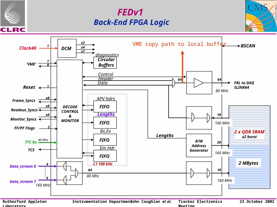
FEDv1 Back-End FPGA Logic
FIFO
FIFO
FIFO
FIFO
CircularBuffers
Frame_Syncs
Readout_Syncs
Monitor_Syncs
x8
x8
x8
TTC Rx
TCS
‘VME’
DECODECONTROL
&MONITOR
Data_stream 0
Data_stream 7
64 18Data In
20Address
18 Data Out
64FRL to DAQSLINK64
64
R/WAddress
Generator
APV hdrs
Lengths
Bx,Ex
Em Hdr
diagnostics
Data
80 Mhz
L1 100 kHz4
4
160 MHz
40 Mhz
Clock40
Reset
DCMx1
x2x4
2 x QDR SRAMx2 burst
BSCAN
160 MHz
160 MHz
160 MHz
80 MHz
Lengths
Header
FF/PF Flags 2
8
1
1
1
Control
2 MBytes
VME copy path to local buffer

Instrumentation Department John Coughlan et al.Rutherford Appleton Laboratory 23 October 2002Tracker Electronics Meeting
FEDv1 Status
VME-FPGA
TTCrx
BE-FPGAEvent Builder
Buffers
FPGAConfiguration
PowerDC-DC
DAQInterface
12
12
12
12
12
12
12
12
Front-End Modules x 8Double-sided board
CERNOpto-
Rx Analogue/Digital
96 TrackerOpto Fibres
VMEInterface
XilinxVirtex-IIFPGA
FE-FPGAClusterFinder
TTC
TCS
TempMonitor
JTAG
TCS : Trigger Control System
9U VME64x
Hardware:Analogue Design CompleteDigital Design CompletePower Design CompleteFirmware:Delay CompleteCluster Finding CompleteEvent Building 50% DoneVME Interface 25% DoneBoard:Layout & Routing Front-End Module
CompleteBack-End Layout doneRouting started
Manufacture Tape out to PCB week 46Testing Start at RAL week 50
Board Status
•Design effort now re-directed to completing Firmware. Team is sufficient.
•Design is progressing well.

Instrumentation Department John Coughlan et al.Rutherford Appleton Laboratory 23 October 2002Tracker Electronics Meeting
FEDv1 Module Testing Firmware Functionality
•VME interface A32/D32 only
•Raw Data events only (unpacked)
•Scope mode for timing
•TTC interface ?
•Individual ADC clock skews
•Hardware trigger throttle ?
•S-LINK
•TCS interface
•Cluster Finding Firmware
•In-situ Firmware updates
•Auto-Calibration
•VME64x dynamic addressing
•Board hot swapping
Essential Non Essential
Q. What event rate needed for testing?Q. What features? Do we need individual channel DAC offsets ? (or is common OptoRx offset sufficient)
Note: Firmware is tested (simulation/dev boards) but “real world” often has surprises.

Instrumentation Department John Coughlan et al.Rutherford Appleton Laboratory 23 October 2002Tracker Electronics Meeting
FEDv1 Low-Level Software
XDAQ Hardware Abstraction Layer
•we need to learn more but...
•fedlib C++ class API lowest level access structures & functions for user programs (object contained in fed class?)
•fedlib calls HAL read/write functions
Hide details/sequences from user.
int fedlib_load_fe_peds(fe_mod, struct peds,..)
•Maybe additional layer above fedlib? (see Costas’s talk)
•Assume PC Linux + HAL supported VME Interface card
fedlib
fed taskfed task
user space

Instrumentation Department John Coughlan et al.Rutherford Appleton Laboratory 23 October 2002Tracker Electronics Meeting
FEDv1 Address Map
Hidden from outside world…
•But need this before fedlib API
•Address Map under construction. Implementation tightly coupled to Firmware.
•Probably reserve < 1 MByte / FED
FE FPGA #0
FE FPGA #1
FE FPGA #2
FE FPGA #3
FE FPGA #4
FE FPGA #5
FE FPGA #6
FE FPGA #7
FED local CSR
TTCrx
Event Memory
FPGA confign
PedestalsSkew values...etc

Instrumentation Department John Coughlan et al.Rutherford Appleton Laboratory 23 October 2002Tracker Electronics Meeting
FEDv1 Parameter Loading
Mechanism of FED setup hidden from User
•e.g. Loading FED parameters not trivial
•Write constants e.g. Peds to small local FPGA buffer. Limited FPGA memory.
•Send command to load to FE FPGA
•FPGA “engine” handles serial commands
•Optional readback
•Repeat for next block reusing same parameter area
Constraints:
•Can’t load individual channels
•NB can’t access constants during Run!
Command & Status
ParameterLoad block
ParameterReadback block
under development
Instrumentation Department John Coughlan et al.Rutherford Appleton Laboratory 23 October 2002Tracker Electronics Meeting
FEDv1 Firmware & Software
VME-FPGA
TTCrx
BE-FPGAEvent Builder
Buffers
FPGAConfiguration
PowerDC-DC
DAQInterface
12
12
12
12
12
12
12
12
Front-End Modules x 8Double-sided board
CERNOpto-
Rx Analogue/Digital
96 TrackerOpto Fibres
VMEInterface
XilinxVirtex-IIFPGA
Digital Processing
Flexible Digital Logic:
Xilinx Virtex-II FPGAs 40K->3M gates*
*some in pin compatible packages
Features:
Dual Ported Block Rams
Digital Clock Managers DCM
Double Data Rate I/O DDR
Digitally Controlled Impedance I/O
Various I/O signal standards
Debugging: Logic Analyser cores
FPGAs programmed in
VHDL & VERILOG
FE-FPGAClusterFinder
TTC
TCS
TempMonitor
JTAG
TCS : Trigger Control System
9U VME64x

Instrumentation Department John Coughlan et al.Rutherford Appleton Laboratory 23 October 2002Tracker Electronics Meeting
FEDv1 Database Requirements
Per FED 25 K strips
Per Strip: 256 x 96
Pedestals @ 10 bits
Cluster Thresholds @ 2 x 8 bits
Enable bits @ 1 bits
Per APV: 2 x 96
Enable @ 2 bits
Per ADC: 1 x 96
Skew @ 8 bits
Frame Thresholds @ 5 bits
Control @ 2 bits
DACs @ 8 bits
Per OptoRx: 1 x 8
Control @ 8 bits
+...
TTCrx settings
FPGA configuration
FED run settings
FED ID
Total ~ 100 KBytes +

Instrumentation Department John Coughlan et al.Rutherford Appleton Laboratory 23 October 2002Tracker Electronics Meeting
FEDv1 Event Readout
DAQ Trailer
FormattedFED Data
DAQ Header
Tracker Header?
Readout (via VME) Formatted Events identical? to those sent to S-LINK
•Load Parameters e.g. Peds, Skews
•Set run mode e.g. Raw Data, TTC clock
•Start Run and wait for Triggers/Frames
•Poll on Event Counter
•Get length of event
•(Request to) Readout (in chunks)
•Clear Event & Repeat…
•Check local status registers/counters
i.e. similar to PMC (sorry)
Event Formats:
Raw Data unprocessed.
Scope Mode.
Tracker header?
Instrumentation Department John Coughlan et al.Rutherford Appleton Laboratory 23 October 2002Tracker Electronics Meeting
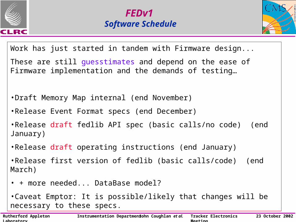
FEDv1 Software Schedule
Work has just started in tandem with Firmware design...
These are still guesstimates and depend on the ease of Firmware implementation and the demands of testing…
•Draft Memory Map internal (end November)
•Release Event Format specs (end December)
•Release draft fedlib API spec (basic calls/no code) (end January)
•Release draft operating instructions (end January)
•Release first version of fedlib (basic calls/code) (end March)
• + more needed... DataBase model?
•Caveat Emptor: It is possible/likely that changes will be necessary to these specs.

Instrumentation Department John Coughlan et al.Rutherford Appleton Laboratory 23 October 2002Tracker Electronics Meeting
FEDv1 Comments
•In order to achieve minimum firmware & software on TIB timescales require...
•Confirmation of functionality needed for TIB tests.
•Close co-operation between UK and Tracker DAQ group.
•Arrange small FEDv1 online meeting.
•Propose contact from UK to visit CERN for “technology transfer”.
•Keep systems h/w and s/w as close as possible (within UK) and between UK and CERN.
•Note: We now have additional effort in UK for test software, database, etc.
•See Testing Talk

Instrumentation Department John Coughlan et al.Rutherford Appleton Laboratory 23 October 2002Tracker Electronics Meeting
FEDv1 Testing

Instrumentation Department John Coughlan et al.Rutherford Appleton Laboratory 23 October 2002Tracker Electronics Meeting
FEDv1 CratesComments
• 2 FEDv1s to test in UK starting December 2002
• FEDv1 is a complex board.
• Board evaluation will require considerable time and effort
• Originally aiming for Batch 2 delivery 10? FEDs to CERN Q4 2003
• Testing Design: Hardware Optical/Analogue/Digital & Firmware
• i.e. Boards aren’t ready one month after receiving them
• Problems will happen
• Need for special Test Firmware & Software
• Common set-ups within UK and with CERN (see Costas’s talk)

Instrumentation Department John Coughlan et al.Rutherford Appleton Laboratory 23 October 2002Tracker Electronics Meeting
FEDv1 Test Features
VME-FPGA
TTCrx
BE-FPGAEvent Builder
Buffers
FPGAConfiguration
PowerDC-DC
DAQInterface
12
12
12
12
12
12
12
12
Front-End Modules x 8Double-sided board
CERNOpto-
Rx Analogue/Digital
96 TrackerOpto Fibres
VMEInterface
XilinxVirtex-IIFPGA
JTAG Boundary Scan: Digital integrity/connections
Electrical Analogue Integrity Tests pre OptoRx
Xilinx “Chip Scope” Integrated Logic Analyser Cores : Capture raw ADC data (pre VME interface)
Opto-Tests with IC Test Board
Special FPGA loads e.g. Pattern Generators
Additional Test Features:
Internal/External Clocks
External Triggers
FE-FPGAClusterFinder
TTC
TCS
TempMonitor
JTAG
TCS : Trigger Control System
9U VME64x

Instrumentation Department John Coughlan et al.Rutherford Appleton Laboratory 23 October 2002Tracker Electronics Meeting
FEDv1Test Plan Draft
CMS-FED FF1 Test Plan
Historyv 0.1 02.09.02 JAC First Draft. First stages of testing described.
Incomplete effort/time estimates.
IntroductionThis document describes the test plan for the full-scale 9U prototypes of the CMS FED FF1.The test plan concentrates on the procedures and resources needed for verifying the correctness of thedesign (both analogue and digital) of the first pair of FF1 boards (001 & 002.)
It is expected that this plan will evolve into that required for larger scale production board testing.
The testing will be conducted in parallel at RAL and ICL.Tests first conducted at RAL unless marked.
Tests are shown approximately in time sequence.
Pre-Assembly Bare Board TestsPCB company should perform bare board tests.At RAL boards must be visually inspected for visible defects.Multi-meter tests of all power rails to check for short circuits[1 day].
Post Assembly (pre OptoRx)Assembly company should visually inspect (automated process?)At RAL attach unique (3 digit) serial number label.Route card must be kept for each assembled board (web accessible.)
Carry out a thorough visual inspection of each board.Inspect assembled PCBs for missing or incorrect components, solder bridges, shorts on power rails andgeneral visible damage.Multi-meter tests of power rails for shorts.[2 days]
Power Supply ChecksRequires VME64x Crate & Power Supply (could this also be done with just PS brick?)Optional VME64x extender board
Power on board.Check that appropriate Power LEDs are lit.Check that warning LEDs are NOT lit (e.g. over-temperature warning.)Measure voltages at specified probe points.Record results in spread sheets.[2 days]
•Test effort in UK shared:
RAL Electrical & Digital
IC Optical
•UK test team is sufficient
•Design vs Production testing
•Integrity vs Performance testing
•Hardware vs Firmware* tests
•Originally foresaw ~ 9 months design testing before Batch 2
*firmware still under development
Test Plan Draft

Instrumentation Department John Coughlan et al.Rutherford Appleton Laboratory 23 October 2002Tracker Electronics Meeting
FEDv1Testing Schedule
•Preparation Crates/PSUs/Test Kits/Tools licenses (pre Boards)
•Pre & Post Assembly tests (~1 week)
•Basic Power Supply tests (~1 week)
•Digital Integrity: Boundary Scan JTAG (~1 week)
•FPGA configuration test JTAG (~1 week)
•Analogue Integrity*: Signal Gen/Test card + Chip Scope/JTAG (~4 weeks)
•(Pre VME, board default settings but requires Firmware for Clock set-up in all FPGAs)
•=> Assemble OptoRx Parallel Tests @ IC
•Opto Integrity tests at IC : with IC Opto-Test card + Chip Scope (~4 weeks)
•Basic Digital tests : CFlash FPGA configuration, Clocks TTCrx, QDRs (~6 weeks)
•(Pre VME, Test card + ChipScope , requires special test Firmware)
•VME Interface test : PC & VME Link (~4 weeks)
•(Peek & Poke => Test software)
•Intermediate Digital Tests (Scope mode, Raw Data mode, Event readout) (~8 weeks)
•Intermediate Analogue Tests (Pedestals, X-Talk, Step Response) (~6 weeks)
Instrumentation Department John Coughlan et al.Rutherford Appleton Laboratory 23 October 2002Tracker Electronics Meeting
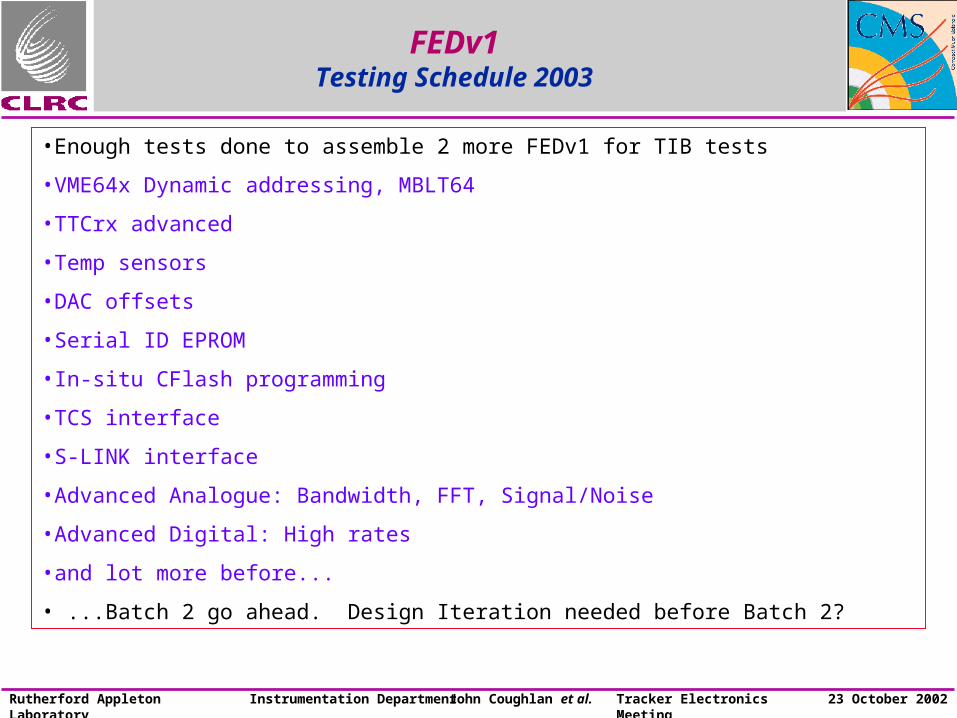
FEDv1Testing Schedule 2003
•Enough tests done to assemble 2 more FEDv1 for TIB tests
•VME64x Dynamic addressing, MBLT64
•TTCrx advanced
•Temp sensors
•DAC offsets
•Serial ID EPROM
•In-situ CFlash programming
•TCS interface
•S-LINK interface
•Advanced Analogue: Bandwidth, FFT, Signal/Noise
•Advanced Digital: High rates
•and lot more before...
• ...Batch 2 go ahead. Design Iteration needed before Batch 2?
Instrumentation Department John Coughlan et al.Rutherford Appleton Laboratory 23 October 2002Tracker Electronics Meeting
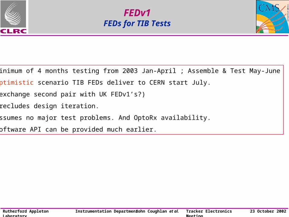
FEDv1FEDs for TIB Tests
•Minimum of 4 months testing from 2003 Jan-April ; Assemble & Test May-June
•Optimistic scenario TIB FEDs deliver to CERN start July.
•(exchange second pair with UK FEDv1’s?)
•Precludes design iteration.
•Assumes no major test problems. And OptoRx availability.
•Software API can be provided much earlier.

Instrumentation Department John Coughlan et al.Rutherford Appleton Laboratory 23 October 2002Tracker Electronics Meeting
FEDv1Test Setups & Software
• Test rig being set up at IC: Crate, PC/Linux + VME Interface
• Clone system at RAL
• Analogue Test piggyback card at RAL (1 -> 12 chans)
• Opto Test VME Card at IC (12 -> 96 chans)
• Plus TTC systems, FEDKit
• XDAQ/HAL based fedlib library
• Dedicated UK Test software also using same fedlib library.
• Needed in UK in March.
• Firmware development continuing in parallel.
•Q. Suitable GUI for test software Qt ? Used LabView in past.
Instrumentation Department John Coughlan et al.Rutherford Appleton Laboratory 23 October 2002Tracker Electronics Meeting
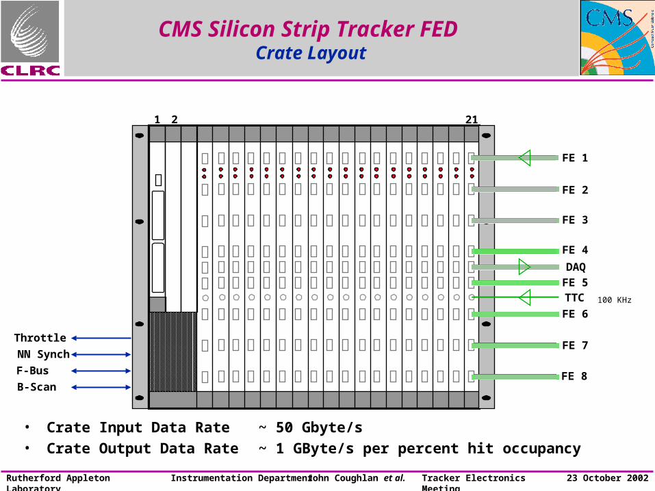
CMS Silicon Strip Tracker FED Crate Layout
1 212
FE 1
DAQ
TTC
FE 2
FE 3
FE 4
FE 5
FE 6
FE 7
• Crate Input Data Rate ~ 50 Gbyte/s• Crate Output Data Rate ~ 1 GByte/s per percent hit occupancy
B-Scan
F-Bus
NN Synch
100 KHz
FE 8
Throttle

Instrumentation Department John Coughlan et al.Rutherford Appleton Laboratory 23 October 2002Tracker Electronics Meeting
CMS Silicon Strip Tracker FED Counting Room Layout (illustration)
• 440 Boards 96 ADC/Board
• 24 Crates
• 8 Racks
• 440 Boards 96 ADC/Board
• 24 Crates
• 8 Racks
• 40 K ADC Channels 10 Bit@40MHz• Max Trigger Rate 100 kHz• Input Rate 1.5 T Byte/s• Output rate 25 Gbyte/s/%
• 40 K ADC Channels 10 Bit@40MHz• Max Trigger Rate 100 kHz• Input Rate 1.5 T Byte/s• Output rate 25 Gbyte/s/% 4 TTC Partitions
DAQFED

Instrumentation Department John Coughlan et al.Rutherford Appleton Laboratory 23 October 2002Tracker Electronics Meeting
1 24
E-Net Switch
FECCRATES DCS
Tracker Control WS
TTCCRATES
DAQ
VME SBCRTOS
CMS Silicon Strip Tracker FED Control & Monitoring
D-BASER/C
50K ADC Channels
FEDCRATES